JP4679244B2 - Contact terminal for measurement, measurement device, probe card set, and wafer prober device - Google Patents
Contact terminal for measurement, measurement device, probe card set, and wafer prober device Download PDFInfo
- Publication number
- JP4679244B2 JP4679244B2 JP2005154648A JP2005154648A JP4679244B2 JP 4679244 B2 JP4679244 B2 JP 4679244B2 JP 2005154648 A JP2005154648 A JP 2005154648A JP 2005154648 A JP2005154648 A JP 2005154648A JP 4679244 B2 JP4679244 B2 JP 4679244B2
- Authority
- JP
- Japan
- Prior art keywords
- probe
- contact
- terminal
- measurement
- probe pin
- Prior art date
- Legal status (The legal status is an assumption and is not a legal conclusion. Google has not performed a legal analysis and makes no representation as to the accuracy of the status listed.)
- Expired - Fee Related
Links
- 239000000523 sample Substances 0.000 title claims description 377
- 238000005259 measurement Methods 0.000 title claims description 169
- 238000012360 testing method Methods 0.000 claims description 74
- 239000000758 substrate Substances 0.000 claims description 62
- 230000005540 biological transmission Effects 0.000 claims description 24
- 239000004065 semiconductor Substances 0.000 claims description 18
- 238000001514 detection method Methods 0.000 claims description 13
- 230000008054 signal transmission Effects 0.000 claims description 12
- 238000000034 method Methods 0.000 claims description 8
- 239000000463 material Substances 0.000 claims description 4
- 230000008569 process Effects 0.000 claims description 4
- 238000010586 diagram Methods 0.000 description 16
- 238000003825 pressing Methods 0.000 description 14
- 230000006866 deterioration Effects 0.000 description 8
- 238000013461 design Methods 0.000 description 6
- 230000008859 change Effects 0.000 description 3
- 239000004020 conductor Substances 0.000 description 3
- 238000004519 manufacturing process Methods 0.000 description 3
- 238000005070 sampling Methods 0.000 description 3
- 230000008901 benefit Effects 0.000 description 2
- 238000012937 correction Methods 0.000 description 2
- 238000006073 displacement reaction Methods 0.000 description 2
- 230000007246 mechanism Effects 0.000 description 2
- 239000003990 capacitor Substances 0.000 description 1
- 238000004140 cleaning Methods 0.000 description 1
- 230000008602 contraction Effects 0.000 description 1
- 230000003247 decreasing effect Effects 0.000 description 1
- 230000002950 deficient Effects 0.000 description 1
- 230000001419 dependent effect Effects 0.000 description 1
- 239000000428 dust Substances 0.000 description 1
- 238000012986 modification Methods 0.000 description 1
- 230000004048 modification Effects 0.000 description 1
- 230000000630 rising effect Effects 0.000 description 1
- 238000012546 transfer Methods 0.000 description 1
- 230000007704 transition Effects 0.000 description 1
Images


Classifications
-
- G—PHYSICS
- G01—MEASURING; TESTING
- G01R—MEASURING ELECTRIC VARIABLES; MEASURING MAGNETIC VARIABLES
- G01R35/00—Testing or calibrating of apparatus covered by the other groups of this subclass
- G01R35/005—Calibrating; Standards or reference devices, e.g. voltage or resistance standards, "golden" references
-
- G—PHYSICS
- G01—MEASURING; TESTING
- G01R—MEASURING ELECTRIC VARIABLES; MEASURING MAGNETIC VARIABLES
- G01R1/00—Details of instruments or arrangements of the types included in groups G01R5/00 - G01R13/00 and G01R31/00
- G01R1/02—General constructional details
- G01R1/06—Measuring leads; Measuring probes
- G01R1/067—Measuring probes
- G01R1/06711—Probe needles; Cantilever beams; "Bump" contacts; Replaceable probe pins
-
- G—PHYSICS
- G01—MEASURING; TESTING
- G01R—MEASURING ELECTRIC VARIABLES; MEASURING MAGNETIC VARIABLES
- G01R1/00—Details of instruments or arrangements of the types included in groups G01R5/00 - G01R13/00 and G01R31/00
- G01R1/02—General constructional details
- G01R1/06—Measuring leads; Measuring probes
- G01R1/067—Measuring probes
- G01R1/06772—High frequency probes
-
- G—PHYSICS
- G01—MEASURING; TESTING
- G01R—MEASURING ELECTRIC VARIABLES; MEASURING MAGNETIC VARIABLES
- G01R1/00—Details of instruments or arrangements of the types included in groups G01R5/00 - G01R13/00 and G01R31/00
- G01R1/02—General constructional details
- G01R1/06—Measuring leads; Measuring probes
- G01R1/067—Measuring probes
- G01R1/073—Multiple probes
- G01R1/07307—Multiple probes with individual probe elements, e.g. needles, cantilever beams or bump contacts, fixed in relation to each other, e.g. bed of nails fixture or probe card
-
- G—PHYSICS
- G01—MEASURING; TESTING
- G01R—MEASURING ELECTRIC VARIABLES; MEASURING MAGNETIC VARIABLES
- G01R31/00—Arrangements for testing electric properties; Arrangements for locating electric faults; Arrangements for electrical testing characterised by what is being tested not provided for elsewhere
- G01R31/28—Testing of electronic circuits, e.g. by signal tracer
- G01R31/2851—Testing of integrated circuits [IC]
- G01R31/2886—Features relating to contacting the IC under test, e.g. probe heads; chucks
- G01R31/2891—Features relating to contacting the IC under test, e.g. probe heads; chucks related to sensing or controlling of force, position, temperature
Description
本発明は、半導体試験装置等におけるプローブピンの伝送特性を測定するための測定用コンタクト端子、プローブピンの伝送特性を測定する測定装置、およびプローブピンと測定用コンタクト端子とを有するプローブカードセットに関する。 The present invention relates to a measurement contact terminal for measuring the transmission characteristic of a probe pin in a semiconductor test apparatus or the like, a measurement apparatus for measuring the transmission characteristic of a probe pin, and a probe card set having a probe pin and a measurement contact terminal.
半導体回路等の被試験デバイスを試験する試験装置において、被試験デバイスと接触し、試験装置本体と被試験デバイスとを電気的に接続するプローブカードが用いられている。当該プローブカードは、被試験デバイスの入出力ピンと接触する複数のプローブピンを有する。これらのプローブピンは、予め定められた伝送特性を有するように設計されるが、製造バラツキ等により、それぞれのプローブピンの伝送特性には誤差が生じる。 2. Description of the Related Art In a test apparatus that tests a device under test such as a semiconductor circuit, a probe card that contacts the device under test and electrically connects the test apparatus main body and the device under test is used. The probe card has a plurality of probe pins that come into contact with input / output pins of the device under test. These probe pins are designed to have a predetermined transmission characteristic, but due to manufacturing variations and the like, an error occurs in the transmission characteristic of each probe pin.
プローブピンの伝送特性に誤差が生じている場合、被試験デバイスを精度よく試験することができないので、被試験デバイスを試験する前に、それぞれのプローブピンの伝送特性を測定し、それぞれのプローブピンを介して伝送する信号を補正する必要がある。 If there is an error in the transmission characteristics of the probe pins, the device under test cannot be tested accurately. Therefore, before testing the device under test, measure the transmission characteristics of each probe pin. It is necessary to correct the signal transmitted through the network.
従来、プローブピンの伝送特性を測定する目的で、試験装置からプローブピンに信号を伝送し、プローブピンから出力される信号を測定する方法が知られている。当該方法は、プローブピンが出力する信号を、プローブピンと接触させた測定用コンタクト端子を介して受け取り、信号波形を測定する。 Conventionally, for the purpose of measuring transmission characteristics of a probe pin, a method of transmitting a signal from a test apparatus to the probe pin and measuring a signal output from the probe pin is known. In this method, a signal output from a probe pin is received via a measurement contact terminal brought into contact with the probe pin, and a signal waveform is measured.
このような測定を行う測定用コンタクト端子として、所定の間隔で設けられた信号ピンと、接地ピンとを有する測定用コンタクト端子が知られている。当該測定用コンタクト端子は、信号ピンを、伝送特性を測定するべきプローブピンに接触させ、接地ピンを、接地電位が与えられるプローブピンに接触させることにより、プローブピンが出力する信号を検出する。 As a measurement contact terminal for performing such a measurement, a measurement contact terminal having a signal pin and a ground pin provided at a predetermined interval is known. The measurement contact terminal detects a signal output from the probe pin by bringing the signal pin into contact with the probe pin whose transmission characteristics are to be measured and bringing the ground pin into contact with the probe pin to which the ground potential is applied.
関連する特許文献等は、現在認識していないので、その記載を省略する。 Since related patent documents and the like are not currently recognized, the description thereof is omitted.
しかし、従来の測定用コンタクト端子の接地ピンは、一つのプローブピンと接触できるだけの幅を有するので、信号ピンおよび接地ピンの間隔と、伝送特性を測定するべきプローブピンと、接地電位が与えられるプローブピンとの間隔とが一致していない場合、信号波形を検出することができなかった。このため、従来の測定装置は、信号ピンおよび接地ピンの間隔が異なる複数の測定用コンタクト端子を有する必要があった。 However, since the ground pin of the conventional measurement contact terminal has a width that can contact with one probe pin, the distance between the signal pin and the ground pin, the probe pin for measuring the transmission characteristics, and the probe pin to which the ground potential is applied If the interval does not match, the signal waveform could not be detected. For this reason, the conventional measuring apparatus needs to have a plurality of measurement contact terminals having different intervals between the signal pins and the ground pins.
また、プローブピンは寿命のある部品である。プローブピンは、製造初期の段階では、所定の寸法精度の製造規格内にある。例えば、複数のプローブピンの相対位置、高さバラツキ、接触抵抗等が所定の規格内となるように形成される。しかし、被試験デバイスであるウエハ面へ数万回〜数十万回のコンタクト動作が繰り返し実施される結果、プローブピンの弾性疲労、接触部位の電気的な磨耗及び劣化が進む。また、高温条件で試験が行われるので、温度ストレスによる形状変化及び劣化も受ける。これに伴って、プローブピンの接触抵抗の劣化、物理的な位置ずれ等の劣化に伴うコンタクト不良も発生する。このため、プローブピンの位置、接触抵抗等の特性を測定する必要がある。 Also, the probe pin is a component with a long life. The probe pin is within a manufacturing standard with a predetermined dimensional accuracy at an early stage of manufacture. For example, the plurality of probe pins are formed such that relative positions, height variations, contact resistances, and the like are within a predetermined standard. However, as a result of repeated contact operations of several tens of thousands to several hundreds of thousands of times on the wafer surface, which is the device under test, the probe pin is subject to elastic fatigue and electrical wear and deterioration of the contact area. Further, since the test is performed under a high temperature condition, it undergoes shape change and deterioration due to temperature stress. In connection with this, the contact failure accompanying deterioration of contact resistance of a probe pin, physical position shift, etc. also generate | occur | produces. For this reason, it is necessary to measure characteristics such as the position of the probe pin and the contact resistance.
このため本発明は、上述した課題を解決することのできる測定用コンタクト端子、測定装置、およびプローブカードセットを提供することを目的とする。この目的は、請求の範囲における独立項に記載の特徴の組み合わせにより達成される。また従属項は本発明の更なる有利な具体例を規定する。 For this reason, an object of this invention is to provide the contact terminal for a measurement which can solve the subject mentioned above, a measuring apparatus, and a probe card set. This object is achieved by a combination of features described in the independent claims. The dependent claims define further advantageous specific examples of the present invention.
上記課題を解決するために、本発明のひとつの形態においては、プローブ基板の表面の所定の配列方向において所定の間隔で平行に配列された複数のプローブピンのうちの所望のプローブピンと、外部の測定装置との間で信号伝送を行う測定用コンタクト端子であって、信号端子と、接地電位が与えられ、配列方向における信号端子の両側に設けられた2つの接地端子と、信号端子と、外部の測定装置の信号入力端子とを電気的に接続する信号線と、信号端子および2つの接地端子が固定される接点固定部と、接点固定部に対して一端が固定され、他端が外部の測定装置に固定されるコンタクト固定部とを備え、信号端子および2つの接地端子は、コンタクト固定部の他端が外部の測定装置に固定された状態で、プローブピンと接触する接触面が、プローブ基板の表面に対して角度を有するように設けられる測定用コンタクト端子が与えられる。In order to solve the above problems, in one embodiment of the present invention, a desired probe pin out of a plurality of probe pins arranged in parallel at a predetermined interval in a predetermined arrangement direction on the surface of the probe substrate, and an external A measurement contact terminal for transmitting signals to and from a measuring device, which is provided with a signal terminal, two ground terminals provided on both sides of the signal terminal in the arrangement direction, a signal terminal, and an external terminal A signal line for electrically connecting the signal input terminal of the measuring device, a contact fixing part to which the signal terminal and the two ground terminals are fixed, one end fixed to the contact fixing part, and the other end to the outside A contact fixing portion fixed to the measuring device, and the signal terminal and the two ground terminals are in contact with the probe pin in a state where the other end of the contact fixing portion is fixed to the external measuring device. But the contact terminal for measurement provided is given as an angle relative to the surface of the probe substrate.
信号端子は、配列方向において、一のプローブピンの両側に設けられたプローブピンの間隔より小さい幅を有し、2つの接地端子は、配列方向において、信号端子より大きい幅をそれぞれ有してよい。信号端子の幅は、所定の間隔より小さくてよい。 The signal terminal has a width smaller than the interval between the probe pins provided on both sides of one probe pin in the arrangement direction, and the two ground terminals may have a width larger than the signal terminal in the arrangement direction, respectively. . The width of the signal terminal may be smaller than a predetermined interval.
それぞれの接地端子の幅は、プローブピンの幅と所定の間隔との和より大きくてよい。配列方向におけるそれぞれの接地端子は、信号端子が複数のプローブピンのうちの配列方向における中央に設けられたプローブピンと接触した場合に、当該プローブピンの配列方向における両側に設けられた複数のプローブピンの全てと接触できる幅を有してよい。 The width of each ground terminal may be larger than the sum of the width of the probe pin and the predetermined interval. Each ground terminal in the arrangement direction has a plurality of probe pins provided on both sides in the arrangement direction of the probe pins when the signal terminal contacts the probe pin provided in the center in the arrangement direction among the plurality of probe pins. The width may be in contact with all of the above.
信号端子においてプローブピンと接触する接触面、および2つの接地端子においてプローブピンと接触する接触面は、略同一の平面に設けられてよい。接地端子は、接地電位が与えられる半導体基板であり、信号端子は、半導体基板の配列方向における略中央に、半導体プロセスにより形成されてよい。 The contact surface that contacts the probe pin in the signal terminal and the contact surface that contacts the probe pin in the two ground terminals may be provided on substantially the same plane. The ground terminal is a semiconductor substrate to which a ground potential is applied, and the signal terminal may be formed by a semiconductor process substantially at the center in the arrangement direction of the semiconductor substrate.
信号端子および2つの接地端子は、非弾性材料で形成されてよい。コンタクト固定部は、プローブ基板と略平行な測定装置に固定される平板部を有し、信号端子および2つの接地端子は、プローブピンと接触する接触面が、コンタクト固定部の平板部に対して角度を有するように設けられてよい。 The signal terminal and the two ground terminals may be formed of an inelastic material. The contact fixing part has a flat plate part fixed to a measuring device substantially parallel to the probe substrate, and the signal terminal and the two ground terminals have an angle with respect to the flat part of the contact fixing part that makes contact with the probe pin. May be provided.
信号端子および2つの接地端子は、接点固定部のプローブピンに対向する端辺から、プローブピンに向かう方向に突出して設けられてよい。 The signal terminal and the two ground terminals may be provided so as to protrude in a direction toward the probe pin from an end side of the contact fixing portion facing the probe pin.
本発明の他の形態においては、プローブ基板と、プローブ基板の表面の所定の配列方向において所定の間隔で平行に配列されたプローブピンと、一端が試験装置に接続され、他端が対応するプローブピンに接続される伝送経路とを備えるプローブカードに対して、それぞれのプローブピンおよび伝送経路の信号伝送特性を測定する測定装置であって、複数のプローブピンのうち、信号伝送特性を測定するべき被測定プローブピンと電気的に接続される、請求項1から10のいずれか一項に記載の測定用コンタクト端子と、被測定プローブピンが出力する出力信号を測定用コンタクト端子を介して受け取り、出力信号に基づいて、被測定プローブピンと、被測定プローブピンに対応する伝送経路との信号伝送特性を測定する測定部とを備える測定装置が与えられる。 In another embodiment of the present invention, a probe board, probe pins arranged in parallel at a predetermined interval in a predetermined arrangement direction on the surface of the probe board, one end connected to the test apparatus, and the other end corresponds to the corresponding probe pin A probe card having a transmission path connected to the probe card, and measuring signal transmission characteristics of each probe pin and transmission path. The measurement contact terminal according to any one of claims 1 to 10, which is electrically connected to the measurement probe pin, and an output signal output from the probe pin to be measured are received via the measurement contact terminal, and an output signal is received. Based on the measurement probe pin and a measurement unit for measuring the signal transmission characteristics of the transmission path corresponding to the probe pin to be measured. Device is given.
当該測定装置は、プローブカードに対する測定用コンタクト端子の位置を検出する位置検出部と、位置検出部が検出した位置に基づいて、測定用コンタクト端子の位置を制御し、測定用コンタクト端子と被測定プローブピンとを電気的に接続する位置制御部とを更に備え、位置制御部は、プローブカードの表面における所定の方向に対する、信号端子および接地端子の配設方向の角度を調整可能に、測定用コンタクト端子を保持してよい。 The measurement device controls the position of the measurement contact terminal based on the position detected by the position detection unit and the position detection unit that detects the position of the measurement contact terminal with respect to the probe card. A position control unit that electrically connects the probe pin, and the position control unit is capable of adjusting the angle of the arrangement direction of the signal terminal and the ground terminal with respect to a predetermined direction on the surface of the probe card, and the contact for measurement. You may hold the terminal.
本発明の他の形態においては、被試験デバイスと試験装置とを電気的に接続するプローブカードと、プローブカードの信号伝送特性を測定するための請求項1から10のいずれか一項に記載の測定用コンタクト端子とを備えるプローブカードセットであって、プローブカードは、プローブ基板と、プローブ基板の表面の所定の配列方向において所定の間隔で平行に配列されたプローブピンと、一端が試験装置に接続され、他端が対応するプローブピンに接続される伝送経路とを有するプローブカードセットが与えられる。 In another aspect of the present invention, the probe card for electrically connecting the device under test and the test apparatus, and signal transmission characteristics of the probe card are measured according to any one of claims 1 to 10. A probe card set including a measurement contact terminal, the probe card being connected to a test board, probe pins arranged in parallel at predetermined intervals in a predetermined arrangement direction on the surface of the probe board, and one end connected to a test apparatus And a probe card set having a transmission path whose other end is connected to a corresponding probe pin.
本発明の他の形態においては、ウエハ上に形成された被試験デバイスの電極に対応する位置へプローブカードのプローブピンを移動させる移動ステージを備え、被試験デバイスの電気的特性を試験するウエハプローバ装置であって、プローブカードに設けられたプローブピンの先端部に電気的に接触し、先端部における電気信号を検出する、請求項1から10のいずれか一項に記載の測定用コンタクト端子を備え、ウエハプローバ装置は、信号端子と接地端子とに接続され、信号端子における電気信号を測定する測定部と、測定用コンタクト端子を、互いに直交する3軸の方向に移動させ、信号端子を、電気的特性を測定するべきプローブピンに押圧接触する3軸移動装置とを更に備えるウエハプローバ装置が与えられる。 In another embodiment of the present invention, a wafer prober that includes a moving stage that moves probe pins of a probe card to a position corresponding to an electrode of a device under test formed on a wafer, and tests the electrical characteristics of the device under test. 11. The measurement contact terminal according to claim 1, wherein the measurement contact terminal is in electrical contact with a tip portion of a probe pin provided on the probe card and detects an electrical signal at the tip portion. The wafer prober apparatus is connected to a signal terminal and a ground terminal, and moves a measurement unit for measuring an electrical signal at the signal terminal and a measurement contact terminal in directions of three axes orthogonal to each other, A wafer prober apparatus is further provided, further comprising a triaxial moving device that presses and contacts the probe pins whose electrical characteristics are to be measured.
なお、上記の発明の概要は、本発明の必要な特徴の全てを列挙したものではなく、これらの特徴群のサブコンビネーションもまた、発明となりうる。 The above summary of the invention does not enumerate all the necessary features of the present invention, and sub-combinations of these feature groups can also be the invention.
以下、発明の実施の形態を通じて本発明を説明するが、以下の実施形態は特許請求の範囲にかかる発明を限定するものではなく、また実施形態の中で説明されている特徴の組み合わせの全てが発明の解決手段に必須であるとは限らない。 Hereinafter, the present invention will be described through embodiments of the invention. However, the following embodiments do not limit the invention according to the scope of claims, and all combinations of features described in the embodiments are included. It is not necessarily essential for the solution of the invention.
図1は、本発明の実施形態に係る、測定装置100の構成の一例を示す図である。測定装置100は、半導体回路等を試験する試験装置54が備えるプローブカード20の信号波形及び電気的特性を測定する。ここで、移動ステージ60及びウエハチャック62は、ウエハプローバ装置が備えている構成要素である。ウエハチャック62は、ウエハ90を真空吸着して保持する。
FIG. 1 is a diagram illustrating an example of a configuration of a
試験装置54は、本体部52、テストヘッド28、カードホルダ25、およびプローブカード20を有する。本体部52は、ウエハ90に形成される被試験デバイスに供給する試験信号を生成し、被試験デバイスが出力する出力信号に基づいて被試験デバイスの良否を判定する。テストヘッド28は、カードホルダ25及びプローブカードを保持し、本体部52との間で信号の授受を行う。
The
カードホルダ25は、プローブカード20を交換可能に保持固定する。また、カードホルダ25は、テストヘッド28とプローブカード20との間で信号伝送を仲介する。
The
プローブカード20は、ウエハ90上に形成された被試験デバイスの電極にコンタクトして電気信号の授受を行うものであり、プローブ基板23および複数のプローブピン22を有する。プローブピン22は、プローブ基板23の表面に、被試験デバイスの複数の入出力ピンと対応する位置に設けられる。また、それぞれのプローブピン22は、伝送経路56を介してテストヘッド28に接続される。このような構成により、試験装置54は、被試験デバイスに試験信号を供給し、また出力信号を受け取る。
The
測定装置100は、位置検出部10、測定部12、位置制御部14、測定用コンタクト端子16、駆動部18、及び移動ステージ60を有する。測定用コンタクト端子16は、プローブ基板23と対向して設けられ、複数のプローブピンのうち、信号伝送特性を測定するべき被測定プローブピンと電気的に接続される。測定用コンタクト端子16は、それぞれのプローブピン22の先端と接触するべく、それぞれ直交するX軸、Y軸、Z軸の3軸で移動可能であることが好ましい。例えば、図1に示すように、測定用コンタクト端子16は、ウエハ90を3軸で移動させる移動ステージ60に取り付けられてよい。また、測定装置100、プローブカード20、及び移動ステージ60により、ウエハプローバ装置を形成する。移動ステージ60は、被試験デバイスの試験実行時において、ウエハ90をウエハチャック(図示せず)で真空吸着して、X軸、Y軸、Z軸の3軸においてウエハ90を移動させ、プローブカード20とコンタクトさせる。
The
位置検出部10は、プローブカード20に対する測定用コンタクト端子16の位置を検出する。位置検出部10は、CCD撮像素子10a及び3軸移動装置10bを備える。3軸移動装置10bは、CCD撮像素子10aを所望の位置へ移動させる。CCD撮像素子10aは、測定用コンタクト端子16の画像を取得する。位置検出部10は、CCD撮像素子10aが取得した画像に基づいて測定用コンタクト端子16の位置を検出する。また、CCD撮像素子10aは、プローブピン22の画像をあわせて取得し、位置検出部10は、プローブピン22の位置、及び測定用コンタクト端子16とプローブピン22との相対位置を検出する。3軸移動装置10bは、移動ステージ60と独立した移動系であってよい。また、CCD撮像素子10aは、移動ステージ60において、測定用コンタクト端子16に対して所定の位置に取り付けられていてもよい。
The
位置制御部14は、位置検出部10が検出した当該位置に基づいて、測定用コンタクト端子16の位置を制御し、測定用コンタクト端子16と被測定プローブピンとを電気的に接続する。駆動部18は、移動ステージ60に固定され、移動ステージ60の移動に連動して3軸方向に移動する。また、駆動部18は、測定用コンタクト端子16を保持する。移動ステージ60は、位置制御部14から与えられる制御信号に基づいて、駆動部18に取り付けられた測定用コンタクト端子16の位置を変動させる。尚、本例において駆動部18は、移動ステージ60に取り付けられ、移動ステージ60の移動と連動して移動するが、他の例においては、駆動部18は、移動ステージ60と独立した移動系を有してよい。また、駆動部18は、3軸移動装置10bに取り付けられていてもよい。後者の場合、CCD撮像素子10aと、測定用コンタクト端子16との相対位置を常に維持することができる。
The
測定部12は、それぞれのプローブピン22の先端位置における電気的特性(伝搬遅延タイミング、波形形状、波形品質、波形歪み、立ち上がりエッジ及び立ち下がりエッジの波形品質、振幅、電圧レベル、その他の電気的特性)を測定する。測定部12は、被測定プローブピンの先端における出力信号を、測定用コンタクト端子16を介して受け取り、当該出力信号に基づいて、テストヘッド28の出力端から伝送経路56を介して被測定プローブピンに至る信号伝送品質、最終端の電気的特性を測定する。当該信号伝送特性を測定する場合、試験装置54は、当該被測定プローブピンに所定の信号を発生させ、他のプローブピン22に接地電位を発生させる。ここで、伝搬遅延タイミングを測定する場合には、テストヘッド28から測定部12へ基準タイミング信号を供給する。例えば、基準タイミング信号に対する、それぞれの被測定プローブピンに発生させた信号の遅延時間を測定することにより、各々の被測定プローブピン間のタイミングスキューが精度よく測定できる。
The measuring
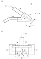
図2は、測定用コンタクト端子16が有する接点部44、および複数のプローブピン22の上面拡大図である。図2(a)は、接点部44の構造の一例を示し、図2(b)は、接点部44の構造の他の例を示す。
FIG. 2 is an enlarged top view of the
図2に示すように、複数のプローブピン22は、プローブ基板23の表面の所定の配列方向において所定の間隔L3で平行して配置される。また本例において、一のプローブピン22の両側のプローブピンの間隔はL2であり、複数のプローブピン22が設けられる領域の幅はL5である。
As shown in FIG. 2, the plurality of probe pins 22 are arranged in parallel at a predetermined interval L <b> 3 in a predetermined arrangement direction on the surface of the
接点部44は、伝送特性を測定するべきプローブピン22と接触する信号端子26、および信号端子26の両側に設けられた2つの接地端子24を有する。プローブピン22の配列方向における、信号端子26の幅L1は、少なくともL2より小さい。これにより、信号端子26は、一つのプローブピン22と接触することができる。また、信号端子26の幅L1は、L3より小さいことが好ましい。これにより、信号端子26が複数のプローブピン22と接触することを防ぐことができる。すなわち、信号端子26は、一つのプローブピンと電気的に接触し、当該プローブピンと電気的に接触したときに、他のプローブピンとは電気的に接触しない導体幅を有する。
The
例えば、プローブピン22のピンピッチ(L2−L3)が100μmであり、隣接するピンの間隔L3が50μmより大きいとき、信号端子26の幅L1は、50μmであってよい。
For example, when the pin pitch (L2-L3) of the probe pins 22 is 100 μm and the interval L3 between adjacent pins is larger than 50 μm, the width L1 of the
それぞれの接地端子24は、信号端子26より大きく、複数のプローブピン22と接触できる幅を有する。例えば、接地端子24は、一つのプローブピン22の幅と、プローブピン22の間隔L3との和より大きい幅を有する。このような構成により、それぞれの接地端子24は、複数のプローブピン22に接触する。すなわち、接地端子24は、信号端子26が一つのプローブピン22と電気的に接触したときに、当該プローブピン22に隣接して設けられた複数のプローブピンに対して電気的に接触する導体幅又は平面導体を有する。このため、当該複数のプローブピン22のいずれかが接地ピンであれば、接地端子24は信号端子26の直近で接地できる。このため、当該プローブピン22の先端部位における電気的特性を的確に測定可能となる利点が得られる。
Each
尚、複数のプローブピン22のいずれも接地ピンで無い可能性もある。しかし、図8に示すように、複数のプローブピン22b〜22eの遠端側に接続されているドライバ59がゼロ電位が駆動されているので、接地端子24の電位に関しては低いインピーダンス状態となり、実用的に電気的特性が測定できる。尚、接地端子24の他の構造例として、信号端子26の片側にのみ接地端子24を設けてもよく、信号端子26の全周に接地端子24を設けてもよい。
Note that there is a possibility that none of the plurality of probe pins 22 is a ground pin. However, as shown in FIG. 8, since the driver 59 connected to the far end side of the plurality of probe pins 22b to 22e is driven with a zero potential, the potential of the
また、接地端子24は、信号端子26が複数のプローブピン22のうちの配列方向における中央に設けられたプローブピン22と接触した場合に、当該中央のプローブピン22の配列方向における両側に設けられた複数のプローブピン22の全てと接触できる幅を有することが好ましい。つまり、接点部44の幅L4は、複数のプローブピン22が設けられる領域の幅L5と略等しいことが好ましい。例えば、ピンピッチが100μmであり、61本のプローブピンからなるプローブピン群と接触する場合、接点部44の幅L4は、6100μmであってよい。このような構成により、伝送特性を測定するべきプローブピン22を挟む、いずれか2つのプローブピン22が接地ピンであれば、接地端子24は、少なくともいずれかの接地ピンと接触するので、接地端子24は接地電位を検出することができる。
The
また、それぞれの接地端子24の幅は、複数のプローブピン22が設けられる領域の幅と略等しくてよい。これにより、信号端子26がどのプローブピン22と接触した場合であっても、接地端子24は、他の全てのプローブピン22と接触することができる。
The width of each
また、信号端子26においてプローブピン22と接触する接触面、および2つの接地端子24においてプローブピン22と接触する接触面は、略同一の平面に設けられることが好ましい。例えば、信号端子26および2つの接地端子24は、同一の基板上に形成されてよい。また、信号端子26および2つの接地端子は、非弾性材料で形成されることが好ましい。これにより、接点部44は、複数のプローブピンと同時に接触することができる。
Further, the contact surface that contacts the
図2(b)は、接点部44の上面拡大図の他の例を示す。本例における接点部44は、同一の基板に、信号端子26および接地端子24が形成される。例えば、接地端子24は、接地電位が与えられる半導体基板により形成され、信号端子26は、プローブピン22の配列方向における当該半導体基板の略中央に、半導体プロセスにより形成される。また、信号端子26は、当該半導体基板の表面から裏面まで貫通して形成され、当該半導体基板のプローブピン22と対向する端辺から、プローブピン22の長手方向と略平行な方向に、所定の長さを有して形成される。この場合、幅の小さいプローブピン22を容易に形成することができる。
FIG. 2B shows another example of an enlarged top view of the
また、プローブ基板23には、複数の被試験デバイスと電気的に接続するべき、平行して設けられたプローブピン群が複数設けられてよい。このとき、それぞれのプローブピン群における配列方向は異なる場合がある。駆動部18は、それぞれのプローブピン群と測定用コンタクト端子16とが接触できるように、プローブ基板23の表面における所定の方向に対する、信号端子26および接地端子24の配設方向の角度を調整可能に、測定用コンタクト端子16を保持することが好ましい。つまり、それぞれのプローブピン群の配列方向に対して、信号端子26および接地端子24の配設方向を略平行にすることができるように、駆動部18は、測定用コンタクト端子16を保持する。
In addition, the
図3は、測定用コンタクト端子16の構成の一例を示す図である。図3(a)は、測定用コンタクト端子16の側面図を示し、図3(b)は、図3(a)におけるAの方向から見た測定用コンタクト端子16の正面図を示す。
FIG. 3 is a diagram illustrating an example of the configuration of the
測定用コンタクト端子16は、同軸ケーブル30、接点固定部42、コンタクト固定部36、同軸端子40、および接点部44を有する。接点部44は、プローブピン22と接触する端子である。同軸ケーブル30は、測定部12と、接点部44とを電気的に接続する信号線である。また、同軸端子40は、同軸ケーブル30から延伸して設けられ、接点部44と電気的に接続される。これにより、同軸ケーブル30の信号線は信号端子26と接続され、接地線は接地端子24に接続される。
The
接点固定部42は、接点部44を固定する。例えば、接点固定部42は、接点部44が載置される底面部と、底面部の両端から上方に延伸する延伸部を有する。接点固定部42は、両端の延伸部により接点部44の両側を挟み込むことにより、接点部44を固定する。また、接点部44は、接点固定部42のプローブピン22に対向する端辺50から、プローブピン22に向かう方向に突出して固定される。
The
コンタクト固定部36は板形状であり、一端が接点固定部42に固定され、他端が駆動部18に固定される。これにより、測定用コンタクト端子16は、駆動部18に固定される。また、コンタクト固定部36は、同軸ケーブル30を保持する。コンタクト固定部36には、同軸ケーブル30の同軸端子40を貫通させる貫通孔が形成され、同軸端子40は、当該貫通孔を介して接点部44に接触する。
The
図4は、駆動部18に固定された測定用コンタクト端子16を示す図である。プローブピン22は、プローブ基板23の表面に対して角度を有して設けられる。このため、測定用コンタクト端子16の接点部44は、プローブピン22と接触する面がプローブ基板23の表面に対して角度を有して設けられることが好ましい。この場合、プローブ基板23の表面に対する接点部44の当該接触面の角度が、プローブ基板23の表面に対するプローブピン22の角度と略同一となるように、測定用コンタクト端子16を駆動部18に固定することが好ましい。
FIG. 4 is a diagram showing the
コンタクト固定部36は、平板部32、延伸部34、およびケーブル固定部38を有する。駆動部18は、プローブ基板23の表面と略平行な平面部を有し、平板部32は、当該平面部に固定される。また、延伸部34は、平板部32からプローブ基板23の方向に延伸して設けられ、平板部32に対して所定の角度を有する。また、接点固定部42の底面は、延伸部34と略平行に設けられ、接点部44は、当該底面と略平行に設けられる。このため、接点部44は、プローブピン22と接触する接触面が、平板部32に対して角度を有するように設けられる。このような構成により、測定用コンタクト端子16を、プローブピン群22−1に接触させた場合に、他のプローブピン群22−2と測定用コンタクト端子16とが接触することを防ぐことができる。
The
延伸部34は、平板部32が駆動部18に固定された場合に、接点部44の角度とプローブピン22の角度とが略同一となるように、平板部32から角度を有して延伸して設けられることが好ましい。また、ケーブル固定部38は、延伸部34から更に延伸して設けられ、同軸ケーブル30を固定する。
The extending
また、接点部44が、接点固定部42から突出する長さL6は、プローブピン22と接点部44が接触した場合に、プローブピン22が湾曲した場合であっても、プローブピン22との接続を保つことができる程度に長いことが好ましい。
Further, the length L6 of the
図5は、駆動部18に固定された測定用コンタクト端子16の他の例を示す図である。本例における測定用コンタクト端子16の接点部44は、プローブ基板23の表面と略平行な接触面を有する。プローブ基板23の表面と略平行な接触面を有することにより、試験装置54が被試験ウエハを試験する場合と同一の接触条件における、それぞれのプローブピンの伝送特性を測定することができる。
FIG. 5 is a diagram illustrating another example of the
本例におけるコンタクト固定部36は、平板部32を有さず、延伸部34において、駆動部18に固定される。延伸部34は、接点固定部42の底面と略平行な面を有し、当該面において駆動部18に固定される。これにより、接点固定部42の底面は、プローブ基板23の表面と略平行に保持される。また、接点部44は、段差部49に固定され、段差部49は、接点固定部42に固定される。段差部49及び接点部44は、同一の半導体基板から形成されてよい。例えば、接点部44は、当該半導体基板の裏面に形成されたパターンであってよい。また、接点部44と同軸ケーブル30とは、例えば段差部49に形成されたスルーホールを介して電気的に接続される。
The
このような構造により、測定用コンタクト端子16の接点部44以外の箇所が、接点部44の接触面より下側に突出することを防ぐことができる。このため、被測定プローブピン群と接点部44が接触した場合に、当該接触面以外の箇所が、他のプローブピン群と接触することを防ぐことができる。例えば、プローブ基板23の表面には、複数のプローブピン群(22−1〜22−4)が、所定の間隔L22で形成される。複数のプローブピン群の配列方向における接点固定部42の縦幅が、間隔L22より大きい場合であっても、段差部49を設けることにより、接点固定部42が、被測定対象のプローブピン群以外に接触することを防ぐことができる。段差部49の厚さは、プローブピン22が測定用コンタクト端子16により押圧されて湾曲した場合に生じる、プローブ基板23の鉛直方向におけるプローブピン22の高さの変動より大きいことが好ましい。
With such a structure, it is possible to prevent a portion other than the
また、駆動部18は、接点部44の接触面が、プローブ基板23の表面と略平行となるように、測定用コンタクト端子16を保持する角度を調整する手段を有していることが好ましい。これにより、被測定プローブピンのそれぞれのプローブピン22に対して、均一に押圧を加えることができる。例えば、図1において説明した位置検出部10が、接点部44の接触面の角度を検出し、駆動部18は、当該角度に基づいて、測定用コンタクト端子16を保持する角度を調整してよい。
The
図6(a)及び図6(b)は、接点部44の構造例を示す図である。図6(a)及び図6(b)は、共に接点部44の底面図及び正面図を示す。接点部44において、プローブ基板23と対向する底面には、接地端子24及び信号端子26が形成される。接点部44は、半導体基板であって、接地端子24及び信号端子26は、半導体プロセスによって形成されてよい。
FIG. 6A and FIG. 6B are diagrams illustrating a structure example of the
図6(a)及び図6(b)に示すように、信号端子26は、接点部44の基板におけるプローブピン22の配列方向と平行な辺の略中央から、当該基板の内側に当該辺と垂直な方向に延伸して設けられる。また、接地端子24は、当該基板の面の略全体に渡って設けられる。接地端子24は、信号端子26が設けられた当該基板の辺において、信号端子26と所定の間隔を有して設けられ、当該辺以外における信号端子26の3辺を囲むように設けられる。
As shown in FIG. 6A and FIG. 6B, the
また、接点部44の基板、及び段差部49には、信号端子26及び接地端子24と同軸ケーブル30とを電気的に接続するためのスルーホール25が形成される。同軸ケーブル30の信号線及び接地線は、スルーホール25を介して信号端子26及び接地端子24と接続される。
In addition, a through
また、図6(b)に示すように、接点部44は、長い縦幅D45を有していてもよい。例えば、縦幅D45は、図5において説明したプローブピン群の間隔L22より大きくてよい。これにより、接点部44は、複数のプローブピン群と接触することができる。複数のプローブピン群と接触することにより、当該複数のプローブピン群のいずれかのプローブピン22が接地ピンであれば、接地端子24は、当該接地ピンと接触することができる。また、当該複数のプローブピン群に複数の接地ピンが含まれている場合、接地端子24は、より多くの接地ピンと接触することができる。尚、接点部44の接触平面に対して微少に角度変位できるヨーイング補正機構を備えることが望ましい。
Moreover, as shown in FIG.6 (b), the
図7は、測定用コンタクト端子16と、測定部12との間における電気的な接続を説明する図である。図7(a)に示すように、測定用コンタクト端子16と測定部12とは、同軸ケーブル30を介して電気的に接続される。この場合、同軸ケーブル30の一端において、信号線が信号端子26に接続され、接地線が接地端子24に接続される。また、同軸ケーブル30の他端は、測定部12の入力端子13に接続され、測定用コンタクト端子16から受け取った信号を、測定部12に伝送する。
FIG. 7 is a diagram illustrating electrical connection between the
また、他の例においては、図7(b)に示すように、信号端子26と、同軸ケーブル30の信号線との間に抵抗R27を設け、測定部12の入力端子を抵抗R11で終端してもよい。抵抗R27の抵抗値は、例えば450Ω、又は4950Ωであって、抵抗R11の抵抗値は、例えば50Ωである。このように抵抗を設けることにより、信号伝送経路は、1/10、又は1/100の減衰特性を有する。また、抵抗R27の両端に、波形補償用のコンデンサを設けることが望ましい。このような構造により、高インピーダンスで測定対象のプローブピン22に接続できるので、プローブピン22が伝送する波形をより精度よく測定することができる。特に、急峻な波形の高速パルスに対して、より良好に測定することができる。
In another example, as shown in FIG. 7B, a resistor R27 is provided between the
また、測定装置100は、図7(a)及び図7(b)に示した伝送経路を受ける2チャンネルの入力端子13を備え、2つの測定用コンタクト端子16を備える構成としてもよい。この場合、測定するべき波形に応じて、的確な波形品質で測定することができる。
Further, the measuring
次に、プローブピン22の接触抵抗の測定例を説明する。図8は、テストヘッド28の構成の一例を示す図である。テストヘッド28は、複数のスイッチ(57a〜57f、以下57と総称する)、複数のドライバ(59a〜59f、以下59と総称する)、コンパレータ61、及び電源部63を有する。本例において、プローブピン22a〜22fは、接地端子24に接続されるピンである。また、電源部63は、電流印加電圧測定装置(ISVM)であってよい。ここで、テストヘッド28には、被試験デバイスのIC端子に接続する多数のI/Oチャンネル(ドライバ59fとコンパレータ61とを組み合わせたチャンネル)、及びドライバ専用チャンネル(ドライバ59a〜59e)が設けられる。
Next, an example of measuring the contact resistance of the
複数のドライバ59は、複数のプローブピン22と対応して設けられ、本体部52から受け取った信号を、対応するプローブピン22に供給する。但し、本例においてプローブピン22dは接地ピンであり、接地電位が与えられる。
The plurality of drivers 59 are provided corresponding to the plurality of probe pins 22, and supply the signals received from the
複数のスイッチ57は、複数のプローブピン22と対応し、対応するプローブピン22と、対応するドライバ59との間に設けられる。それぞれのスイッチ57は、対応するプローブピン22を、対応するドライバ59、又は電源部63のいずれに接続するかを切り替える。複数のスイッチ57は、本体部52が制御してよい。コンパレータ61は、被測定プローブピン22a以外の複数のプローブピン22のいずれかに対して、ドライバ59と並列に設けられ、対応するプローブピン22が外部から受け取った信号の電圧値を測定する。本例において、コンパレータ61は、当該プローブピン22が接地端子24から受け取る電圧値を測定する。
The plurality of switches 57 correspond to the plurality of probe pins 22 and are provided between the corresponding probe pins 22 and the corresponding drivers 59. Each switch 57 switches whether the
本例において測定装置100は、試験装置54を制御し、プローブ基板23に設けられたプローブピン(22a〜22f)のそれぞれの接触抵抗を測定する。例えば、測定部12が、プローブピン(22a〜22f)のうちのいずれかの接触抵抗を測定する旨を、試験装置54に通知することにより、試験装置54を制御する。また、位置制御部14は、被測定プローブピンを含む複数のプローブピン22に、接地端子24が接触するように、測定用コンタクト端子16の位置を制御する。
In this example, the measuring
また、位置制御部14は、測定用コンタクト端子16の接地端子24が、プローブ基板23に設けられた全てのプローブピン22に順次接触するように、測定用コンタクト端子16の位置を制御してよい。例えば、接地端子24に接触している全てのプローブピン22の接触抵抗を測定した場合に、測定用コンタクト端子16の位置を変更し、未測定のプローブピン群に接地端子24を接触させてよい。
Further, the
プローブピン22aの接触抵抗を測定する場合、スイッチ57aは、プローブピン22aと電源部63とを接続する。他のスイッチ57は、対応するプローブピン22と、ドライバ59とを接続する。また、本体部52は、被測定プローブピンに対応しないドライバ(59b〜59e)に対して、略ゼロ電位を発生させ、ドライバ59fをオフ状態に制御する。
When measuring the contact resistance of the
測定部12は、電源部63から、被測定プローブピン22aに対応するスイッチ57aを介して、被測定プローブピン22aに、所定の定電流i1を供給させる。この場合、当該定電流は、接地端子24を介して他のプローブピン22に流れ、ドライバ(59b〜59e)により接地電位に流れる。
The
また、測定部12は、電源部63が被測定プローブピンに印加した電圧値、接地端子24における電圧値、及び定電流i1の電流値に基づいて、被測定プローブピン22aの接触抵抗を算出する接触抵抗算出手段として機能する。例えば、電源部63からプローブピン22aに印加された電圧値を第1の電圧V2、接地端子24における電圧値を第2の電圧V3とすると、プローブピン22aにおける接触抵抗は、(V2−V3)/i1により算出することができる。
The measuring
プローブピン22aにおける電圧V2は、電源部63が印加する電圧と略等しい。電源部63は、印加した電圧値V2、及び印加した電流値i1を測定部12に通知してよい。また、ドライバ59fはオフ状態であるため、接地端子24からプローブピン22fに対しては電流が流れない。このため、電圧値V3は、コンパレータ61で測定できる。すなわち、コンパレータ61は、電圧測定手段として機能する。測定部12は、コンパレータ61が測定する電圧値を、接地端子24における電圧値V3として取得してよい。
The voltage V2 at the
コンパレータ61は、比較電圧を変更しながらコンパレータ61の出力状態を検出することで電圧値V3を特定できる。これにより、当該電圧値V3を検出し、測定部12に通知してよい。このような制御により、プローブピン22aの接触抵抗を精度よく測定することができる。また、他のプローブピン22の接触抵抗を測定する場合も同様であり、スイッチ57を制御し、測定するべきプローブピン22を電源部63に接続し、他のプローブピン22をドライバ59で接地電位に接続する。
The
次に、全てのプローブピン22の接触抵抗値の良否判定例を説明する。ここで、全てのプローブピン22の中で、接触抵抗値に対する許容値が異なる場合がある。例えば、被試験デバイスの出力端子は、例えば1Ω以下の低い接触抵抗値が要求されるが、入力端子の場合は、例えば10Ω程度の高い接触抵抗値が許容される場合がある。また、複数ピンを備える電源ピン及びアースピンは、全体で例えば0.1Ω以下であれば使用可能である場合がある。 Next, an example of determining whether the contact resistance values of all the probe pins 22 are good or bad will be described. Here, among all the probe pins 22, the allowable value for the contact resistance value may be different. For example, the output terminal of the device under test is required to have a low contact resistance value of, for example, 1Ω or less, but in the case of the input terminal, a high contact resistance value of, for example, about 10Ω may be allowed. In addition, the power supply pin and the ground pin having a plurality of pins may be usable as long as the total is, for example, 0.1Ω or less.
そこで、試験するデバイス品種毎に、又は所定の複数ピンのグループに対して、各々の許容接触抵抗値Rmaxを予め設定し、保存する手段を設ける。そして、上述の接触抵抗の測定で全てのプローブピン22を測定した後、各プローブピンに対応する許容接触抵抗値Rmaxと比較して、許容接触抵抗値Rmaxより大きい場合には、当該プローブピン22を不良として判定する。この結果、プローブカード20の実用可能な寿命を長くできる利点が得られる。尚、当該測定により得られる接触抵抗値の情報は、長期間保存して当該プローブカードの交換時期を判断する情報としても利用できる。
Therefore, means for presetting and storing each allowable contact resistance value Rmax for each device type to be tested or for a predetermined group of a plurality of pins is provided. And after measuring all the probe pins 22 by the measurement of the above-mentioned contact resistance, when compared with the allowable contact resistance value Rmax corresponding to each probe pin, when it is larger than the allowable contact resistance value Rmax, the
次に、プローブピン22の押圧特性の測定例を説明する。測定用コンタクト端子16と、プローブ基板23との押圧方向の距離(押圧距離)を順次変化させて、プローブピン22の接触抵抗を複数回測定することで、プローブピン22の押圧特性を測定できる。プローブピン22に対する押圧力は、当該押圧距離に応じて変化する。当該押圧距離は、位置制御部14が測定用コンタクト端子16の位置を制御することにより、制御することができる。押圧距離毎の接触抵抗値の測定結果から、プローブピン22の接触部位の劣化を確認することができる。
Next, an example of measuring the pressing characteristics of the
また、プローブピン22に対する押圧距離を順次増加させて接触抵抗を測定し、次に、プローブピン22に対する押圧距離を順次減少させて接触抵抗を測定することにより、接触抵抗の、押圧力に対するヒステリシス特性を測定することができる。当該ヒステリシス特性を測定することにより、プローブピン22の接触部位の劣化特性の判断材料が得られる。
Further, the contact resistance is measured with respect to the pressing force by measuring the contact resistance by sequentially increasing the pressing distance to the
また、プローブピン22の接触抵抗を測定した後、プローブピン22に対する押圧力を開放し、再度プローブピン22の接触抵抗を測定することを繰り返すことにより、プローブピン22の電気的接続の信頼性、接触部位に対するごみの付着残留等を確認することができる。また、プローブピン22の接触抵抗の測定は、所定の期間毎に行ってよい。測定結果を蓄積することにより、プローブピン22の経時劣化や、劣化の特異点を特定することができる。これにより、プローブピン22の交換、クリーニング等を、適切な期間で行うことができる。
In addition, after measuring the contact resistance of the
次に、プローブピン22の物理的な位置ずれ状態の測定を説明する。図9〜図11は、測定用コンタクト端子16を用いて、プローブピン22の位置を測定する方法の一例を示す図である。図9及び図10は、プローブ基板23の表面と垂直な方向から見た上面図であり、図11は、プローブ基板23の側面と垂直な方向から見た側面図である。
Next, measurement of the physical displacement state of the
プローブピン22の位置を測定する場合、図8において説明した電源部63は、位置を測定するべきプローブピン22に対し、微小電流に制限した電圧信号を供給する。そして、図1において説明した位置制御部14は、測定用コンタクト端子16の位置を変化させ、プローブ基板23の表面を走査する。位置制御部14は、測定用コンタクト端子16を、プローブ基板23の表面と平行な面において直交するX軸及びY軸方向にそれぞれ移動させることができ、またプローブ基板23の表面の垂直なZ軸方向に移動させることができることが好ましい。
When measuring the position of the
測定部12は、測定用コンタクト端子16の位置毎に、測定用コンタクト端子16に伝送される電源部63の電圧信号を検出する。つまり、測定用コンタクト端子16の信号端子26と、位置を測定するべきプローブピン22とが接触したときに、測定部12が電圧信号を検出する。これにより、位置制御部14が当該プローブピン22をX軸及びY軸方向へ移動制御する位置情報から、当該プローブピン22の検出領域が得られ、これから当該プローブピン22の中心位置が特定できる。他の検出方法としては、当該プローブピン22が接地端子に接触することを利用する検出方法でも行うことができる。この場合、電源部63の出力電圧がゼロ付近になる電圧変化から検出できる。
The
より具体的には、位置制御部14には、プローブ基板23の表面において、それぞれのプローブピン22の配置に関する設計情報が与えられる。そして、位置制御部14は、当該設計情報に基づいて、位置を測定するべきプローブピン22の近傍に測定用コンタクト端子16を移動させる。
More specifically, the
次に、位置制御部14は、図9に示すように、プローブピン群におけるプローブピン22の配列方向(X軸方向)に沿って測定用コンタクト端子16を移動させ、測定するべきプローブピン22のX軸方向における位置を検出する。測定用コンタクト端子16をX軸方向に沿って移動させる場合、位置制御部14は、信号端子26の長手方向と、プローブピン22の長手方向とが略平行となるように、測定用コンタクト端子16の向きを制御することが好ましい。これにより、信号端子26が複数のプローブピン22と同時に接触することを防ぎ、測定するべきプローブピン22の位置を精度よく測定することができる。プローブピン22の長手方向は、設計情報から判別してよい。
Next, as shown in FIG. 9, the
次に、位置制御部14は、検出したX軸方向における位置に信号端子26が配置されるように、測定用コンタクト端子16の位置を制御する。そして、図10に示すように、位置制御部14は、X軸方向と垂直なY軸方向に沿って測定用コンタクト端子16を移動させ、測定するべきプローブピン22のY軸方向における位置を検出する。この場合、位置制御部14は、図10(a)に示すように、信号端子26の長手方向と、プローブピン22の長手方向とが略平行となるように、測定用コンタクト端子16の向きを制御してよく、また図10(b)に示すように、信号端子26の長手方向と、プローブピン22の長手方向とが略垂直となるように、測定用コンタクト端子16の向きを制御してもよい。
Next, the
X軸方向及びY軸方向に測定用コンタクト端子16を移動させる場合、位置制御部14は、信号端子26がプローブピン22の先端部と接触するように、測定用コンタクト端子16のY軸方向における位置を制御することが好ましい。例えば位置制御部14は、測定用コンタクト端子16を、プローブピン22の先端部と接触する高さにおいて、プローブ基板23の表面と略平行な面内で移動させてよい。プローブピン22の先端部のY軸方向における高さは、設計情報から判別してよい。また、プローブピン22が経時変化により変形し、プローブピン22の先端部のY軸方向における位置が、設計値よりも低くなった場合であっても、信号端子26がプローブピン22と接触できるように、位置制御部14は、設計情報から判別されるプローブピン22の先端部のY軸方向における位置よりも低い位置に、信号端子26が配置されるように、測定用コンタクト端子16の位置を制御してよい。
When the
次に、位置制御部14は、検出したX軸方向及びY軸方向における位置に信号端子26が配置されるように、測定用コンタクト端子16の位置を制御する。そして、図11に示すように、位置制御部14は、信号端子26とプローブピン22との距離が小さくなるように、Z軸方向に沿って測定用コンタクト端子16を移動させ、測定するべきプローブピン22のZ軸方向における位置を検出する。位置制御部14は、測定部12が微小電流を検出した場合に、測定用コンタクト端子16の移動を終了する。これにより、プローブピン22に過大な押圧力を印加することを防ぎ、プローブピン22の先端部のZ軸方向における位置を検出することができる。
Next, the
また、位置制御部14は、プローブピン22の位置を検出する場合に、測定用コンタクト端子16の位置を、例えば二分探索法を用いて制御してよい。これにより、測定用コンタクト端子16の移動回数を低減し、効率よくプローブピン22の位置を検出することができる。
Further, when detecting the position of the
以上の測定を、測定するべき全てのプローブピン22に対して行うことにより、全てのプローブピン22の先端部の3次元の位置情報を取得することができる。この場合、電源部63は、測定するべき全てのプローブピン22に、微小な所定電流に制限した電圧信号を順次印加し、測定部12は、測定するべきプローブピン22の先端部のそれぞれの位置を測定し、それぞれのプローブピン22の相対位置ずれを測定する位置測定手段として機能してよい。当該プローブカード20を用いて、被測定デバイスの試験を行う場合に、当該位置情報を用いることにより、被測定デバイスとプローブピン22とを精度よく接続することができる。また、それぞれのプローブピン22の先端部の平坦度から、被試験デバイスの試験を行う場合に、被試験デバイスをプローブピン22に押圧するときのストローク量を精度よく調整することができる。
By performing the above measurement for all the probe pins 22 to be measured, the three-dimensional position information of the tip portions of all the probe pins 22 can be acquired. In this case, the
また、当該測定により得られる位置情報を長期間蓄積することで、プローブピン22の3次元形状の経時変化の推移情報が得られ、プローブピン22の形状の変形及び劣化が特定できる。これにより、例えば、被試験デバイスの試験を行う場合のコンタクト不良を未然に低減することができる。また、プローブピン22の交換時期を適切に判断することができる。
Further, by accumulating the position information obtained by the measurement for a long period of time, it is possible to obtain transition information of the three-dimensional shape change of the
図12は、測定用コンタクト端子16の構成の他の例を示す図である。本例においては、ウエハチャック62で真空吸着可能に測定用コンタクト端子16の底部を形成し、プローブ基板23と対向する面に、プローブ基板23の方向に突出する段差部49を形成し、段差部49のプローブ基板23と対向する面に、接点部44を設ける。この場合、接点部44は大きな平面を容易に形成できるので、大きな面積の接地端子24を容易に形成することができる。
FIG. 12 is a diagram illustrating another example of the configuration of the
尚、測定用コンタクト端子16の形状は、ウエハ90の形状に合わせて、ウエハ90の搬送装置を流用できるようにすることが望ましい。また、接点部44と接続する同軸ケーブル30は、移動ステージ60の移動に伴う伸縮応力が小さくなるように、例えばフレキシブルプリント配線を用いてよい。フレキシブルプリント配線には、例えば50Ωの特性インピーダンスとなるように信号線と接地線とをパターン形成する。この場合、電気的特性を測定しないときは、移動ステージ60から取り外すことができる。但し、測定用コンタクト端子16をウエハチャック62に真空吸着する都度、位置検出器10で吸着位置を特定する。
Note that it is desirable that the shape of the
以上においては、プローブピン群におけるそれぞれのプローブピン22が、図2及び図5に示すように、一列に配列されている場合について説明した。しかし、既知の配列であれば、プローブピン22は一列に配列されていなくとも、例えば図5において説明したコンタクト端子16を用いて電気的特性及び位置情報を測定することができる。
In the above, the case where the probe pins 22 in the probe pin group are arranged in a line as shown in FIGS. 2 and 5 has been described. However, in the case of a known arrangement, even if the probe pins 22 are not arranged in a line, the electrical characteristics and position information can be measured using, for example, the
また以上においては、測定部12は、試験装置54の外部に設けられているが、他の例では、試験装置54が測定部12として機能してもよい。例えば、テストヘッド28に備える多数のI/Oチャンネルのうち、被測定プローブピンに接続されない空きチャンネルを用いて、測定用コンタクト端子16が検出する信号を本体部52に取り込んでもよい。試験装置54は、サンプリングオシロスコープのように、サンプリングタイミングを変化させながらコンパレータ61で電圧レベルを測定する機能を有する。従って、プローブピン22のサンプリング波形を取得することができる。これにより、外部の測定手段を用いずとも、電気的特性等を測定することができる。
In the above description, the
また以上においては、測定用コンタクト端子16の支持構造は、駆動部18に固定される場合について説明したが、他の例においては、測定用コンタクト端子16と駆動部18との間に弾性部材を設け、接点部44の接触平面に対して微少に角度変位できる構造を備えてもよい。これにより、ヨーイング補正機構を備えなくとも、複数のプローブピン22と接点部44との接触平面との間で高さのバラツキがあっても、押圧力を均一化することができる。
In the above description, the support structure for the
以上、本発明を実施の形態を用いて説明したが、本発明の技術的範囲は上記実施の形態に記載の範囲には限定されない。上記実施の形態に、多様な変更または改良を加えることが可能であることが当業者に明らかである。その様な変更または改良を加えた形態も本発明の技術的範囲に含まれ得ることが、特許請求の範囲の記載から明らかである。 As mentioned above, although this invention was demonstrated using embodiment, the technical scope of this invention is not limited to the range as described in the said embodiment. It will be apparent to those skilled in the art that various modifications or improvements can be added to the above-described embodiment. It is apparent from the scope of the claims that the embodiments added with such changes or improvements can be included in the technical scope of the present invention.
以上から明らかなように、本発明によれば、複数のプローブピンの伝送特性を測定するときに、接地ピンとして割り当てられたプローブピンと接触するべき接地端子が、当該接地ピンと容易に接触することができる。 As is apparent from the above, according to the present invention, when measuring the transmission characteristics of a plurality of probe pins, the ground terminal to be in contact with the probe pin assigned as the ground pin can easily come into contact with the ground pin. it can.
10・・・位置検出部、12・・・測定部、14・・・位置制御部、16・・・測定用コンタクト端子、18・・・駆動部、20・・・プローブカード、22・・・プローブピン、23・・・プローブ基板、24・・・接地端子、25・・・ステージ、26・・・信号端子、28・・・テストヘッド、30・・・同軸ケーブル、32・・・平板部、34・・・延伸部、36・・・コンタクト固定部、38・・・ケーブル固定部、40・・・同軸端子、42・・・接点固定部、44・・・接点部、50・・・端辺、52・・・本体部、54・・・試験装置、56・・・伝送経路、100・・・測定装置
DESCRIPTION OF
Claims (14)
信号端子と、
接地電位が与えられ、前記配列方向における前記信号端子の両側に設けられた2つの接地端子と、
前記信号端子と、前記外部の測定装置の信号入力端子とを電気的に接続する信号線と、
前記信号端子および前記2つの接地端子が固定される接点固定部と、
前記接点固定部に対して一端が固定され、他端が外部の測定装置に固定されるコンタクト固定部と
を備え、
前記信号端子および前記2つの接地端子は、前記コンタクト固定部の前記他端が前記外部の測定装置に固定された状態で、前記プローブピンと接触する接触面が、前記プローブ基板の表面に対して角度を有するように設けられる測定用コンタクト端子。 A contact terminal for measurement that transmits a signal between a desired probe pin among a plurality of probe pins arranged in parallel at a predetermined interval in a predetermined arrangement direction on the surface of the probe substrate and an external measurement device. ,
A signal terminal;
A ground potential is provided, and two ground terminals provided on both sides of the signal terminal in the arrangement direction;
A signal line for electrically connecting the signal terminal and a signal input terminal of the external measuring device;
A contact fixing portion to which the signal terminal and the two ground terminals are fixed;
One end is fixed with respect to the contact fixing part, and the other end is provided with a contact fixing part fixed to an external measuring device,
The signal terminal and the two ground terminals are configured such that a contact surface that contacts the probe pin is at an angle with respect to a surface of the probe substrate in a state where the other end of the contact fixing portion is fixed to the external measuring device. Contact terminal for measurement provided to have.
前記2つの接地端子は、前記配列方向において、前記信号端子より大きい幅をそれぞれ有する
請求項1に記載の測定用コンタクト端子。 The signal terminal has a width smaller than an interval between the probe pins provided on both sides of the one probe pin in the arrangement direction,
The measurement contact terminal according to claim 1, wherein the two ground terminals have a width larger than the signal terminal in the arrangement direction.
請求項1または2に記載の測定用コンタクト端子。 The measurement contact terminal according to claim 1, wherein a width of the signal terminal is smaller than the predetermined interval.
請求項1から3のいずれか一項に記載の測定用コンタクト端子。 4. The measurement contact terminal according to claim 1, wherein a width of each of the ground terminals is larger than a sum of a width of the probe pin and the predetermined interval. 5.
請求項1から4のいずれか一項に記載の測定用コンタクト端子。 Each of the ground terminals in the arrangement direction is arranged on both sides of the probe pins in the arrangement direction when the signal terminal comes into contact with the probe pin provided in the center in the arrangement direction among the plurality of probe pins. The contact terminal for measurement according to any one of claims 1 to 4, having a width capable of contacting all of the plurality of probe pins provided.
請求項1から5のいずれか一項に記載の測定用コンタクト端子。 The measurement surface according to claim 1, wherein a contact surface that contacts the probe pin in the signal terminal and a contact surface that contacts the probe pin in the two ground terminals are provided on substantially the same plane. Contact terminal.
前記信号端子は、前記半導体基板の前記配列方向における略中央に、半導体プロセスにより形成される
請求項1から6のいずれか一項に記載の測定用コンタクト端子。 The ground terminal is a semiconductor substrate to which the ground potential is applied;
7. The measurement contact terminal according to claim 1, wherein the signal terminal is formed by a semiconductor process at a substantially center in the arrangement direction of the semiconductor substrate.
請求項1から7のいずれか一項に記載の測定用コンタクト端子。 The contact terminal for measurement according to any one of claims 1 to 7, wherein the signal terminal and the two ground terminals are formed of an inelastic material.
前記信号端子および前記2つの接地端子は、前記プローブピンと接触する接触面が、前記コンタクト固定部の前記平板部に対して角度を有するように設けられる
請求項1から8のいずれか一項に記載の測定用コンタクト端子。 The contact fixing portion has a flat plate portion fixed to the measuring device substantially parallel to the probe substrate,
9. The signal terminal and the two ground terminals are provided such that a contact surface in contact with the probe pin has an angle with respect to the flat plate portion of the contact fixing portion. Contact terminal for measurement.
請求項1から9のいずれか一項に記載の測定用コンタクト端子。 10. The signal terminal and the two ground terminals are provided so as to protrude from an end facing the probe pin of the contact fixing portion in a direction toward the probe pin. 10. Contact terminal for measurement.
複数の前記プローブピンのうち、信号伝送特性を測定するべき被測定プローブピンと電気的に接続される、請求項1から10のいずれか一項に記載の前記測定用コンタクト端子と、
前記被測定プローブピンが出力する出力信号を前記測定用コンタクト端子を介して受け取り、前記出力信号に基づいて、前記被測定プローブピンと、前記被測定プローブピンに対応する前記伝送経路との信号伝送特性を測定する測定部と、
を備える測定装置。 A probe board, probe pins arranged in parallel at a predetermined interval in a predetermined arrangement direction on the surface of the probe board, a transmission path having one end connected to a test apparatus and the other end connected to the corresponding probe pin A measuring device for measuring signal transmission characteristics of each of the probe pins and the transmission path with respect to a probe card comprising:
The contact terminal for measurement according to any one of claims 1 to 10, electrically connected to a measured probe pin whose signal transmission characteristics are to be measured among the plurality of probe pins.
An output signal output from the measured probe pin is received via the measurement contact terminal, and based on the output signal, signal transmission characteristics between the measured probe pin and the transmission path corresponding to the measured probe pin A measurement unit for measuring
A measuring apparatus comprising:
前記位置検出部が検出した位置に基づいて、前記測定用コンタクト端子の位置を制御し、前記測定用コンタクト端子と前記被測定プローブピンとを電気的に接続する位置制御部と、を更に備え、
前記位置制御部は、前記プローブカードの表面における所定の方向に対する、前記信号端子および前記接地端子の配設方向の角度を調整可能に、前記測定用コンタクト端子を保持する請求項11に記載の測定装置。 A position detection unit for detecting the position of the measurement contact terminal with respect to the probe card;
Based on the position detected by the position detection unit, the position of the measurement contact terminal is controlled, and further includes a position control unit for electrically connecting the measurement contact terminal and the probe pin to be measured,
The measurement according to claim 11, wherein the position control unit holds the measurement contact terminal such that an angle of an arrangement direction of the signal terminal and the ground terminal with respect to a predetermined direction on a surface of the probe card can be adjusted. apparatus.
前記プローブカードは、
プローブ基板と、
前記プローブ基板の表面の所定の配列方向において所定の間隔で平行に配列されたプローブピンと、
一端が試験装置に接続され、他端が対応する前記プローブピンに接続される伝送経路と
を有するプローブカードセット。 A probe card for electrically connecting a device under test and a test apparatus, and the measurement contact terminal according to any one of claims 1 to 10 for measuring signal transmission characteristics of the probe card. A probe card set,
The probe card is
A probe substrate;
Probe pins arranged in parallel at predetermined intervals in a predetermined arrangement direction of the surface of the probe substrate;
A probe card set having one end connected to a test apparatus and the other end connected to the corresponding probe pin.
前記プローブカードに設けられたプローブピンの先端部に電気的に接触し、前記先端部における電気信号を検出する、請求項1から10のいずれか一項に記載の前記測定用コンタクト端子を備え、
前記ウエハプローバ装置は、
前記信号端子と前記接地端子とに接続され、前記信号端子における電気信号を測定する測定部と、
前記測定用コンタクト端子を、互いに直交する3軸の方向に移動させ、前記信号端子を、前記電気的特性を測定するべき前記プローブピンに押圧接触する3軸移動装置と
を更に備えるウエハプローバ装置。 A wafer prober apparatus comprising a moving stage for moving probe pins of a probe card to a position corresponding to an electrode of a device under test formed on a wafer, and testing the electrical characteristics of the device under test,
The measurement contact terminal according to any one of claims 1 to 10, wherein the measurement contact terminal according to any one of claims 1 to 10, which electrically contacts a tip of a probe pin provided on the probe card and detects an electric signal at the tip.
The wafer prober apparatus includes:
A measuring unit connected to the signal terminal and the ground terminal and measuring an electrical signal at the signal terminal;
A wafer prober apparatus further comprising: a three-axis moving device that moves the measurement contact terminal in directions of three axes orthogonal to each other, and presses and contacts the signal terminal with the probe pin whose electrical characteristics are to be measured.
Priority Applications (2)
| Application Number | Priority Date | Filing Date | Title |
|---|---|---|---|
| JP2005154648A JP4679244B2 (en) | 2005-05-26 | 2005-05-26 | Contact terminal for measurement, measurement device, probe card set, and wafer prober device |
| US11/438,605 US7474109B2 (en) | 2005-05-26 | 2006-05-22 | Contact terminal for measurement, measurement apparatus, probe card set, wafer probe apparatus, and testing apparatus |
Applications Claiming Priority (1)
| Application Number | Priority Date | Filing Date | Title |
|---|---|---|---|
| JP2005154648A JP4679244B2 (en) | 2005-05-26 | 2005-05-26 | Contact terminal for measurement, measurement device, probe card set, and wafer prober device |
Publications (2)
| Publication Number | Publication Date |
|---|---|
| JP2006329836A JP2006329836A (en) | 2006-12-07 |
| JP4679244B2 true JP4679244B2 (en) | 2011-04-27 |
Family
ID=37523566
Family Applications (1)
| Application Number | Title | Priority Date | Filing Date |
|---|---|---|---|
| JP2005154648A Expired - Fee Related JP4679244B2 (en) | 2005-05-26 | 2005-05-26 | Contact terminal for measurement, measurement device, probe card set, and wafer prober device |
Country Status (2)
| Country | Link |
|---|---|
| US (1) | US7474109B2 (en) |
| JP (1) | JP4679244B2 (en) |
Cited By (1)
| Publication number | Priority date | Publication date | Assignee | Title |
|---|---|---|---|---|
| US11067658B2 (en) | 2018-09-13 | 2021-07-20 | Samsung Electronics Co., Ltd. | Probe card inspection wafer, probe card inspection system, and method of inspecting probe card |
Families Citing this family (18)
| Publication number | Priority date | Publication date | Assignee | Title |
|---|---|---|---|---|
| US20070080697A1 (en) * | 2005-09-27 | 2007-04-12 | Sony Corporation | Semiconductor device tester pin contact resistance measurement |
| US7516385B2 (en) * | 2006-04-28 | 2009-04-07 | Sony Corporation | Test semiconductor device in full frequency with half frequency tester |
| US7786742B2 (en) | 2006-05-31 | 2010-08-31 | Applied Materials, Inc. | Prober for electronic device testing on large area substrates |
| US7906979B2 (en) * | 2007-09-14 | 2011-03-15 | Mayo Foundation For Medical Education And Research | High frequency differential test probe for automated printed wiring board test systems |
| US7876121B2 (en) | 2007-09-14 | 2011-01-25 | Mayo Foundation For Medical Education And Research | Link analysis compliance and calibration verification for automated printed wiring board test systems |
| JP5202401B2 (en) * | 2009-03-16 | 2013-06-05 | 株式会社アドバンテスト | Test apparatus and calibration method |
| JP5542720B2 (en) * | 2011-03-04 | 2014-07-09 | 新光電気工業株式会社 | Transmission apparatus, S-parameter measurement method, and gain adjustment method |
| JP5265746B2 (en) * | 2011-09-22 | 2013-08-14 | 東京エレクトロン株式会社 | Probe device |
| JP6016292B2 (en) * | 2011-10-13 | 2016-10-26 | デクセリアルズ株式会社 | Solar cell measurement jig and solar cell output measurement method |
| JP5796870B2 (en) * | 2011-12-05 | 2015-10-21 | 株式会社日本マイクロニクス | Semiconductor device inspection apparatus and chuck stage used therefor |
| US9470753B2 (en) * | 2012-11-07 | 2016-10-18 | Cascade Microtech, Inc. | Systems and methods for testing electronic devices that include low power output drivers |
| US9766269B2 (en) * | 2012-12-29 | 2017-09-19 | Power Probe TEK, LLC | Conductive test probe |
| TWI580969B (en) * | 2015-04-14 | 2017-05-01 | Mpi Corp | Probe card |
| TWI586973B (en) * | 2016-08-12 | 2017-06-11 | 致茂電子股份有限公司 | Contact detecting circuit for four-terminal measuring device |
| TWI679427B (en) * | 2018-10-01 | 2019-12-11 | 巨擘科技股份有限公司 | Probe card device |
| KR20200051303A (en) * | 2018-11-05 | 2020-05-13 | 에스케이하이닉스 주식회사 | Termination circuit and semiconductor apparatus using the same |
| CN110211522A (en) * | 2019-06-29 | 2019-09-06 | 苏州精濑光电有限公司 | A kind of testing agency of display panel |
| US11264906B2 (en) * | 2019-12-13 | 2022-03-01 | Analog Devices, Inc. | Compound pin driver controller |
Citations (4)
| Publication number | Priority date | Publication date | Assignee | Title |
|---|---|---|---|---|
| JP2000208569A (en) * | 1999-01-14 | 2000-07-28 | Mitsubishi Electric Corp | Measuring method and equipment |
| JP2002100658A (en) * | 2000-09-22 | 2002-04-05 | Sony Corp | Semiconductor device inspection apparatus |
| JP2003510574A (en) * | 1999-09-21 | 2003-03-18 | ローゼンベルガー ホーフフレクベンツテクニック ゲーエムベーハー アンド カンパニー | High frequency measurement probe and method of manufacturing the same |
| JP2003282654A (en) * | 2002-03-20 | 2003-10-03 | Hitachi Ltd | Method of manufacturing semiconductor device |
Family Cites Families (10)
| Publication number | Priority date | Publication date | Assignee | Title |
|---|---|---|---|---|
| JPS641249A (en) * | 1987-06-24 | 1989-01-05 | Hitachi Ltd | Wafer prober |
| JPH01202677A (en) * | 1988-02-08 | 1989-08-15 | Mitsubishi Electric Corp | Apparatus for testing semiconductor circuit |
| US4918374A (en) * | 1988-10-05 | 1990-04-17 | Applied Precision, Inc. | Method and apparatus for inspecting integrated circuit probe cards |
| US5355079A (en) * | 1993-01-07 | 1994-10-11 | Wentworth Laboratories, Inc. | Probe assembly for testing integrated circuit devices |
| US5561377A (en) * | 1995-04-14 | 1996-10-01 | Cascade Microtech, Inc. | System for evaluating probing networks |
| JPH10221365A (en) * | 1996-12-06 | 1998-08-21 | Kobe Steel Ltd | Method and apparatus for inspecting probe card |
| JP3222412B2 (en) * | 1997-10-22 | 2001-10-29 | 株式会社東京カソード研究所 | Probe card inspection method |
| US6239590B1 (en) * | 1998-05-26 | 2001-05-29 | Micron Technology, Inc. | Calibration target for calibrating semiconductor wafer test systems |
| JP3574444B2 (en) * | 2002-08-27 | 2004-10-06 | 沖電気工業株式会社 | Method of measuring contact resistance of probe and method of testing semiconductor device |
| US6724205B1 (en) * | 2002-11-13 | 2004-04-20 | Cascade Microtech, Inc. | Probe for combined signals |
-
2005
- 2005-05-26 JP JP2005154648A patent/JP4679244B2/en not_active Expired - Fee Related
-
2006
- 2006-05-22 US US11/438,605 patent/US7474109B2/en not_active Expired - Fee Related
Patent Citations (4)
| Publication number | Priority date | Publication date | Assignee | Title |
|---|---|---|---|---|
| JP2000208569A (en) * | 1999-01-14 | 2000-07-28 | Mitsubishi Electric Corp | Measuring method and equipment |
| JP2003510574A (en) * | 1999-09-21 | 2003-03-18 | ローゼンベルガー ホーフフレクベンツテクニック ゲーエムベーハー アンド カンパニー | High frequency measurement probe and method of manufacturing the same |
| JP2002100658A (en) * | 2000-09-22 | 2002-04-05 | Sony Corp | Semiconductor device inspection apparatus |
| JP2003282654A (en) * | 2002-03-20 | 2003-10-03 | Hitachi Ltd | Method of manufacturing semiconductor device |
Cited By (1)
| Publication number | Priority date | Publication date | Assignee | Title |
|---|---|---|---|---|
| US11067658B2 (en) | 2018-09-13 | 2021-07-20 | Samsung Electronics Co., Ltd. | Probe card inspection wafer, probe card inspection system, and method of inspecting probe card |
Also Published As
| Publication number | Publication date |
|---|---|
| US20060279304A1 (en) | 2006-12-14 |
| JP2006329836A (en) | 2006-12-07 |
| US7474109B2 (en) | 2009-01-06 |
Similar Documents
| Publication | Publication Date | Title |
|---|---|---|
| JP4679244B2 (en) | Contact terminal for measurement, measurement device, probe card set, and wafer prober device | |
| JP6255914B2 (en) | Inspection jig | |
| US10267848B2 (en) | Method of electrically contacting a bond pad of a device under test with a probe | |
| US6762612B2 (en) | Probe contact system having planarity adjustment mechanism | |
| US7888957B2 (en) | Probing apparatus with impedance optimized interface | |
| US6127831A (en) | Method of testing a semiconductor device by automatically measuring probe tip parameters | |
| TWI407119B (en) | Probe card apparatus having a preselected amount of total compliance | |
| EP1566642A1 (en) | Probe card | |
| US10996242B2 (en) | Probe card and test apparatus including the same | |
| US6023171A (en) | Dual-contact probe tip for flying probe tester | |
| JP2008082734A (en) | Electric contact device, high frequency measuring system, and high frequency measuring method | |
| JP5854879B2 (en) | Non-contact type probe card | |
| TWI427297B (en) | Fixture for circuit board inspection | |
| CN110392839B (en) | Electrical connection device | |
| US20090128172A1 (en) | Calibration board for electronic device test apparatus | |
| US9915682B2 (en) | Non-permanent termination structure for microprobe measurements | |
| KR20020025786A (en) | Calibration Device for Semiconductor Testing Apparatus, Calibration Method and Semiconductor Testing Apparatus | |
| JP5397619B2 (en) | Inspection jig for board inspection | |
| WO2006132243A1 (en) | Inspection device | |
| KR101689515B1 (en) | A probe card | |
| KR102548942B1 (en) | Multi pin test device | |
| KR20070117452A (en) | Substrate inspection tool and substrate inspection device | |
| JP2008205282A (en) | Probe card | |
| JPH0729497Y2 (en) | Multi-pin probe | |
| JP2001153911A (en) | Method and apparatus for inspecting wiring pattern |
Legal Events
| Date | Code | Title | Description |
|---|---|---|---|
| A621 | Written request for application examination |
Free format text: JAPANESE INTERMEDIATE CODE: A621 Effective date: 20080415 |
|
| A977 | Report on retrieval |
Free format text: JAPANESE INTERMEDIATE CODE: A971007 Effective date: 20100805 |
|
| A131 | Notification of reasons for refusal |
Free format text: JAPANESE INTERMEDIATE CODE: A131 Effective date: 20100824 |
|
| A521 | Request for written amendment filed |
Free format text: JAPANESE INTERMEDIATE CODE: A523 Effective date: 20101022 |
|
| A131 | Notification of reasons for refusal |
Free format text: JAPANESE INTERMEDIATE CODE: A131 Effective date: 20101109 |
|
| A521 | Request for written amendment filed |
Free format text: JAPANESE INTERMEDIATE CODE: A523 Effective date: 20110107 |
|
| TRDD | Decision of grant or rejection written | ||
| A01 | Written decision to grant a patent or to grant a registration (utility model) |
Free format text: JAPANESE INTERMEDIATE CODE: A01 Effective date: 20110125 |
|
| A01 | Written decision to grant a patent or to grant a registration (utility model) |
Free format text: JAPANESE INTERMEDIATE CODE: A01 |
|
| A61 | First payment of annual fees (during grant procedure) |
Free format text: JAPANESE INTERMEDIATE CODE: A61 Effective date: 20110201 |
|
| R150 | Certificate of patent or registration of utility model |
Free format text: JAPANESE INTERMEDIATE CODE: R150 |
|
| FPAY | Renewal fee payment (event date is renewal date of database) |
Free format text: PAYMENT UNTIL: 20140210 Year of fee payment: 3 |
|
| FPAY | Renewal fee payment (event date is renewal date of database) |
Free format text: PAYMENT UNTIL: 20140210 Year of fee payment: 3 |
|
| LAPS | Cancellation because of no payment of annual fees |