JP4679244B2 - 測定用コンタクト端子、測定装置、プローブカードセット、およびウエハプローバ装置 - Google Patents
測定用コンタクト端子、測定装置、プローブカードセット、およびウエハプローバ装置 Download PDFInfo
- Publication number
- JP4679244B2 JP4679244B2 JP2005154648A JP2005154648A JP4679244B2 JP 4679244 B2 JP4679244 B2 JP 4679244B2 JP 2005154648 A JP2005154648 A JP 2005154648A JP 2005154648 A JP2005154648 A JP 2005154648A JP 4679244 B2 JP4679244 B2 JP 4679244B2
- Authority
- JP
- Japan
- Prior art keywords
- probe
- contact
- terminal
- measurement
- probe pin
- Prior art date
- Legal status (The legal status is an assumption and is not a legal conclusion. Google has not performed a legal analysis and makes no representation as to the accuracy of the status listed.)
- Expired - Fee Related
Links
- 239000000523 sample Substances 0.000 title claims description 377
- 238000005259 measurement Methods 0.000 title claims description 169
- 238000012360 testing method Methods 0.000 claims description 74
- 239000000758 substrate Substances 0.000 claims description 62
- 230000005540 biological transmission Effects 0.000 claims description 24
- 239000004065 semiconductor Substances 0.000 claims description 18
- 238000001514 detection method Methods 0.000 claims description 13
- 230000008054 signal transmission Effects 0.000 claims description 12
- 238000000034 method Methods 0.000 claims description 8
- 239000000463 material Substances 0.000 claims description 4
- 230000008569 process Effects 0.000 claims description 4
- 238000010586 diagram Methods 0.000 description 16
- 238000003825 pressing Methods 0.000 description 14
- 230000006866 deterioration Effects 0.000 description 8
- 238000013461 design Methods 0.000 description 6
- 230000008859 change Effects 0.000 description 3
- 239000004020 conductor Substances 0.000 description 3
- 238000004519 manufacturing process Methods 0.000 description 3
- 238000005070 sampling Methods 0.000 description 3
- 230000008901 benefit Effects 0.000 description 2
- 238000012937 correction Methods 0.000 description 2
- 238000006073 displacement reaction Methods 0.000 description 2
- 230000007246 mechanism Effects 0.000 description 2
- 239000003990 capacitor Substances 0.000 description 1
- 238000004140 cleaning Methods 0.000 description 1
- 230000008602 contraction Effects 0.000 description 1
- 230000003247 decreasing effect Effects 0.000 description 1
- 230000002950 deficient Effects 0.000 description 1
- 230000001419 dependent effect Effects 0.000 description 1
- 239000000428 dust Substances 0.000 description 1
- 238000012986 modification Methods 0.000 description 1
- 230000004048 modification Effects 0.000 description 1
- 230000000630 rising effect Effects 0.000 description 1
- 238000012546 transfer Methods 0.000 description 1
- 230000007704 transition Effects 0.000 description 1
Images


Classifications
-
- G—PHYSICS
- G01—MEASURING; TESTING
- G01R—MEASURING ELECTRIC VARIABLES; MEASURING MAGNETIC VARIABLES
- G01R35/00—Testing or calibrating of apparatus covered by the other groups of this subclass
- G01R35/005—Calibrating; Standards or reference devices, e.g. voltage or resistance standards, "golden" references
-
- G—PHYSICS
- G01—MEASURING; TESTING
- G01R—MEASURING ELECTRIC VARIABLES; MEASURING MAGNETIC VARIABLES
- G01R1/00—Details of instruments or arrangements of the types included in groups G01R5/00 - G01R13/00 and G01R31/00
- G01R1/02—General constructional details
- G01R1/06—Measuring leads; Measuring probes
- G01R1/067—Measuring probes
- G01R1/06711—Probe needles; Cantilever beams; "Bump" contacts; Replaceable probe pins
-
- G—PHYSICS
- G01—MEASURING; TESTING
- G01R—MEASURING ELECTRIC VARIABLES; MEASURING MAGNETIC VARIABLES
- G01R1/00—Details of instruments or arrangements of the types included in groups G01R5/00 - G01R13/00 and G01R31/00
- G01R1/02—General constructional details
- G01R1/06—Measuring leads; Measuring probes
- G01R1/067—Measuring probes
- G01R1/06772—High frequency probes
-
- G—PHYSICS
- G01—MEASURING; TESTING
- G01R—MEASURING ELECTRIC VARIABLES; MEASURING MAGNETIC VARIABLES
- G01R1/00—Details of instruments or arrangements of the types included in groups G01R5/00 - G01R13/00 and G01R31/00
- G01R1/02—General constructional details
- G01R1/06—Measuring leads; Measuring probes
- G01R1/067—Measuring probes
- G01R1/073—Multiple probes
- G01R1/07307—Multiple probes with individual probe elements, e.g. needles, cantilever beams or bump contacts, fixed in relation to each other, e.g. bed of nails fixture or probe card
-
- G—PHYSICS
- G01—MEASURING; TESTING
- G01R—MEASURING ELECTRIC VARIABLES; MEASURING MAGNETIC VARIABLES
- G01R31/00—Arrangements for testing electric properties; Arrangements for locating electric faults; Arrangements for electrical testing characterised by what is being tested not provided for elsewhere
- G01R31/28—Testing of electronic circuits, e.g. by signal tracer
- G01R31/2851—Testing of integrated circuits [IC]
- G01R31/2886—Features relating to contacting the IC under test, e.g. probe heads; chucks
- G01R31/2891—Features relating to contacting the IC under test, e.g. probe heads; chucks related to sensing or controlling of force, position, temperature
Landscapes
- Physics & Mathematics (AREA)
- General Physics & Mathematics (AREA)
- Measuring Leads Or Probes (AREA)
- Testing Or Measuring Of Semiconductors Or The Like (AREA)
Description
Claims (14)
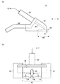
- プローブ基板の表面の所定の配列方向において所定の間隔で平行に配列された複数のプローブピンのうちの所望のプローブピンと、外部の測定装置との間で信号伝送を行う測定用コンタクト端子であって、
信号端子と、
接地電位が与えられ、前記配列方向における前記信号端子の両側に設けられた2つの接地端子と、
前記信号端子と、前記外部の測定装置の信号入力端子とを電気的に接続する信号線と、
前記信号端子および前記2つの接地端子が固定される接点固定部と、
前記接点固定部に対して一端が固定され、他端が外部の測定装置に固定されるコンタクト固定部と
を備え、
前記信号端子および前記2つの接地端子は、前記コンタクト固定部の前記他端が前記外部の測定装置に固定された状態で、前記プローブピンと接触する接触面が、前記プローブ基板の表面に対して角度を有するように設けられる測定用コンタクト端子。 - 前記信号端子は、前記配列方向において、一の前記プローブピンの両側に設けられた前記プローブピンの間隔より小さい幅を有し、
前記2つの接地端子は、前記配列方向において、前記信号端子より大きい幅をそれぞれ有する
請求項1に記載の測定用コンタクト端子。 - 前記信号端子の幅は、前記所定の間隔より小さい
請求項1または2に記載の測定用コンタクト端子。 - それぞれの前記接地端子の幅は、前記プローブピンの幅と前記所定の間隔との和より大きい
請求項1から3のいずれか一項に記載の測定用コンタクト端子。 - 前記配列方向におけるそれぞれの前記接地端子は、前記信号端子が前記複数のプローブピンのうちの前記配列方向における中央に設けられた前記プローブピンと接触した場合に、当該プローブピンの前記配列方向における両側に設けられた複数の前記プローブピンの全てと接触できる幅を有する
請求項1から4のいずれか一項に記載の測定用コンタクト端子。 - 前記信号端子において前記プローブピンと接触する接触面、および前記2つの接地端子において前記プローブピンと接触する接触面は、略同一の平面に設けられる
請求項1から5のいずれか一項に記載の測定用コンタクト端子。 - 前記接地端子は、前記接地電位が与えられる半導体基板であり、
前記信号端子は、前記半導体基板の前記配列方向における略中央に、半導体プロセスにより形成される
請求項1から6のいずれか一項に記載の測定用コンタクト端子。 - 前記信号端子および前記2つの接地端子は、非弾性材料で形成される
請求項1から7のいずれか一項に記載の測定用コンタクト端子。 - 前記コンタクト固定部は、前記プローブ基板と略平行な前記測定装置に固定される平板部を有し、
前記信号端子および前記2つの接地端子は、前記プローブピンと接触する接触面が、前記コンタクト固定部の前記平板部に対して角度を有するように設けられる
請求項1から8のいずれか一項に記載の測定用コンタクト端子。 - 前記信号端子および前記2つの接地端子は、前記接点固定部の前記プローブピンに対向する端辺から、前記プローブピンに向かう方向に突出して設けられる
請求項1から9のいずれか一項に記載の測定用コンタクト端子。 - プローブ基板と、前記プローブ基板の表面の所定の配列方向において所定の間隔で平行に配列されたプローブピンと、一端が試験装置に接続され、他端が対応する前記プローブピンに接続される伝送経路とを備えるプローブカードに対して、それぞれの前記プローブピンおよび前記伝送経路の信号伝送特性を測定する測定装置であって、
複数の前記プローブピンのうち、信号伝送特性を測定するべき被測定プローブピンと電気的に接続される、請求項1から10のいずれか一項に記載の前記測定用コンタクト端子と、
前記被測定プローブピンが出力する出力信号を前記測定用コンタクト端子を介して受け取り、前記出力信号に基づいて、前記被測定プローブピンと、前記被測定プローブピンに対応する前記伝送経路との信号伝送特性を測定する測定部と、
を備える測定装置。 - 前記プローブカードに対する前記測定用コンタクト端子の位置を検出する位置検出部と、
前記位置検出部が検出した位置に基づいて、前記測定用コンタクト端子の位置を制御し、前記測定用コンタクト端子と前記被測定プローブピンとを電気的に接続する位置制御部と、を更に備え、
前記位置制御部は、前記プローブカードの表面における所定の方向に対する、前記信号端子および前記接地端子の配設方向の角度を調整可能に、前記測定用コンタクト端子を保持する請求項11に記載の測定装置。 - 被試験デバイスと試験装置とを電気的に接続するプローブカードと、前記プローブカードの信号伝送特性を測定するための請求項1から10のいずれか一項に記載の前記測定用コンタクト端子とを備えるプローブカードセットであって、
前記プローブカードは、
プローブ基板と、
前記プローブ基板の表面の所定の配列方向において所定の間隔で平行に配列されたプローブピンと、
一端が試験装置に接続され、他端が対応する前記プローブピンに接続される伝送経路と
を有するプローブカードセット。 - ウエハ上に形成された被試験デバイスの電極に対応する位置へプローブカードのプローブピンを移動させる移動ステージを備え、被試験デバイスの電気的特性を試験するウエハプローバ装置であって、
前記プローブカードに設けられたプローブピンの先端部に電気的に接触し、前記先端部における電気信号を検出する、請求項1から10のいずれか一項に記載の前記測定用コンタクト端子を備え、
前記ウエハプローバ装置は、
前記信号端子と前記接地端子とに接続され、前記信号端子における電気信号を測定する測定部と、
前記測定用コンタクト端子を、互いに直交する3軸の方向に移動させ、前記信号端子を、前記電気的特性を測定するべき前記プローブピンに押圧接触する3軸移動装置と
を更に備えるウエハプローバ装置。
Priority Applications (2)
| Application Number | Priority Date | Filing Date | Title |
|---|---|---|---|
| JP2005154648A JP4679244B2 (ja) | 2005-05-26 | 2005-05-26 | 測定用コンタクト端子、測定装置、プローブカードセット、およびウエハプローバ装置 |
| US11/438,605 US7474109B2 (en) | 2005-05-26 | 2006-05-22 | Contact terminal for measurement, measurement apparatus, probe card set, wafer probe apparatus, and testing apparatus |
Applications Claiming Priority (1)
| Application Number | Priority Date | Filing Date | Title |
|---|---|---|---|
| JP2005154648A JP4679244B2 (ja) | 2005-05-26 | 2005-05-26 | 測定用コンタクト端子、測定装置、プローブカードセット、およびウエハプローバ装置 |
Publications (2)
| Publication Number | Publication Date |
|---|---|
| JP2006329836A JP2006329836A (ja) | 2006-12-07 |
| JP4679244B2 true JP4679244B2 (ja) | 2011-04-27 |
Family
ID=37523566
Family Applications (1)
| Application Number | Title | Priority Date | Filing Date |
|---|---|---|---|
| JP2005154648A Expired - Fee Related JP4679244B2 (ja) | 2005-05-26 | 2005-05-26 | 測定用コンタクト端子、測定装置、プローブカードセット、およびウエハプローバ装置 |
Country Status (2)
| Country | Link |
|---|---|
| US (1) | US7474109B2 (ja) |
| JP (1) | JP4679244B2 (ja) |
Cited By (1)
| Publication number | Priority date | Publication date | Assignee | Title |
|---|---|---|---|---|
| US11067658B2 (en) | 2018-09-13 | 2021-07-20 | Samsung Electronics Co., Ltd. | Probe card inspection wafer, probe card inspection system, and method of inspecting probe card |
Families Citing this family (18)
| Publication number | Priority date | Publication date | Assignee | Title |
|---|---|---|---|---|
| US20070080697A1 (en) * | 2005-09-27 | 2007-04-12 | Sony Corporation | Semiconductor device tester pin contact resistance measurement |
| US7516385B2 (en) * | 2006-04-28 | 2009-04-07 | Sony Corporation | Test semiconductor device in full frequency with half frequency tester |
| US7786742B2 (en) | 2006-05-31 | 2010-08-31 | Applied Materials, Inc. | Prober for electronic device testing on large area substrates |
| US7906979B2 (en) * | 2007-09-14 | 2011-03-15 | Mayo Foundation For Medical Education And Research | High frequency differential test probe for automated printed wiring board test systems |
| US7876121B2 (en) | 2007-09-14 | 2011-01-25 | Mayo Foundation For Medical Education And Research | Link analysis compliance and calibration verification for automated printed wiring board test systems |
| JP5202401B2 (ja) * | 2009-03-16 | 2013-06-05 | 株式会社アドバンテスト | 試験装置およびキャリブレーション方法 |
| JP5542720B2 (ja) * | 2011-03-04 | 2014-07-09 | 新光電気工業株式会社 | 伝送装置、sパラメータ測定方法、およびゲイン調整方法 |
| JP5265746B2 (ja) * | 2011-09-22 | 2013-08-14 | 東京エレクトロン株式会社 | プローブ装置 |
| JP6016292B2 (ja) * | 2011-10-13 | 2016-10-26 | デクセリアルズ株式会社 | 太陽電池用測定治具及び太陽電池セルの出力測定方法 |
| JP5796870B2 (ja) * | 2011-12-05 | 2015-10-21 | 株式会社日本マイクロニクス | 半導体デバイスの検査装置とそれに用いるチャックステージ |
| US9470753B2 (en) * | 2012-11-07 | 2016-10-18 | Cascade Microtech, Inc. | Systems and methods for testing electronic devices that include low power output drivers |
| US9766269B2 (en) * | 2012-12-29 | 2017-09-19 | Power Probe TEK, LLC | Conductive test probe |
| TWI580969B (zh) * | 2015-04-14 | 2017-05-01 | Mpi Corp | Probe card |
| TWI586973B (zh) * | 2016-08-12 | 2017-06-11 | 致茂電子股份有限公司 | 四端點量測裝置之接觸檢查電路 |
| TWI679427B (zh) * | 2018-10-01 | 2019-12-11 | 巨擘科技股份有限公司 | 探針卡裝置 |
| KR20200051303A (ko) * | 2018-11-05 | 2020-05-13 | 에스케이하이닉스 주식회사 | 터미네이션 회로 및 이를 사용하는 반도체 장치 |
| CN110211522A (zh) * | 2019-06-29 | 2019-09-06 | 苏州精濑光电有限公司 | 一种显示面板的检测机构 |
| US11264906B2 (en) * | 2019-12-13 | 2022-03-01 | Analog Devices, Inc. | Compound pin driver controller |
Citations (4)
| Publication number | Priority date | Publication date | Assignee | Title |
|---|---|---|---|---|
| JP2000208569A (ja) * | 1999-01-14 | 2000-07-28 | Mitsubishi Electric Corp | 測定装置及び測定方法 |
| JP2002100658A (ja) * | 2000-09-22 | 2002-04-05 | Sony Corp | 半導体装置の検査装置 |
| JP2003510574A (ja) * | 1999-09-21 | 2003-03-18 | ローゼンベルガー ホーフフレクベンツテクニック ゲーエムベーハー アンド カンパニー | 高周波測定プローブ及びその製造方法 |
| JP2003282654A (ja) * | 2002-03-20 | 2003-10-03 | Hitachi Ltd | 半導体装置の製造方法 |
Family Cites Families (9)
| Publication number | Priority date | Publication date | Assignee | Title |
|---|---|---|---|---|
| JPH01202677A (ja) * | 1988-02-08 | 1989-08-15 | Mitsubishi Electric Corp | 半導体回路試験装置 |
| US4918374A (en) * | 1988-10-05 | 1990-04-17 | Applied Precision, Inc. | Method and apparatus for inspecting integrated circuit probe cards |
| US5355079A (en) * | 1993-01-07 | 1994-10-11 | Wentworth Laboratories, Inc. | Probe assembly for testing integrated circuit devices |
| US5561377A (en) * | 1995-04-14 | 1996-10-01 | Cascade Microtech, Inc. | System for evaluating probing networks |
| JPH10221365A (ja) * | 1996-12-06 | 1998-08-21 | Kobe Steel Ltd | プローブカードの検査方法及び装置 |
| JP3222412B2 (ja) * | 1997-10-22 | 2001-10-29 | 株式会社東京カソード研究所 | プローブカード検査方法 |
| US6239590B1 (en) * | 1998-05-26 | 2001-05-29 | Micron Technology, Inc. | Calibration target for calibrating semiconductor wafer test systems |
| JP3574444B2 (ja) * | 2002-08-27 | 2004-10-06 | 沖電気工業株式会社 | プローブの接触抵抗測定方法及び半導体デバイスの試験方法 |
| US6724205B1 (en) * | 2002-11-13 | 2004-04-20 | Cascade Microtech, Inc. | Probe for combined signals |
-
2005
- 2005-05-26 JP JP2005154648A patent/JP4679244B2/ja not_active Expired - Fee Related
-
2006
- 2006-05-22 US US11/438,605 patent/US7474109B2/en not_active Expired - Fee Related
Patent Citations (4)
| Publication number | Priority date | Publication date | Assignee | Title |
|---|---|---|---|---|
| JP2000208569A (ja) * | 1999-01-14 | 2000-07-28 | Mitsubishi Electric Corp | 測定装置及び測定方法 |
| JP2003510574A (ja) * | 1999-09-21 | 2003-03-18 | ローゼンベルガー ホーフフレクベンツテクニック ゲーエムベーハー アンド カンパニー | 高周波測定プローブ及びその製造方法 |
| JP2002100658A (ja) * | 2000-09-22 | 2002-04-05 | Sony Corp | 半導体装置の検査装置 |
| JP2003282654A (ja) * | 2002-03-20 | 2003-10-03 | Hitachi Ltd | 半導体装置の製造方法 |
Cited By (1)
| Publication number | Priority date | Publication date | Assignee | Title |
|---|---|---|---|---|
| US11067658B2 (en) | 2018-09-13 | 2021-07-20 | Samsung Electronics Co., Ltd. | Probe card inspection wafer, probe card inspection system, and method of inspecting probe card |
Also Published As
| Publication number | Publication date |
|---|---|
| US20060279304A1 (en) | 2006-12-14 |
| JP2006329836A (ja) | 2006-12-07 |
| US7474109B2 (en) | 2009-01-06 |
Similar Documents
| Publication | Publication Date | Title |
|---|---|---|
| JP4679244B2 (ja) | 測定用コンタクト端子、測定装置、プローブカードセット、およびウエハプローバ装置 | |
| JP6255914B2 (ja) | 検査治具 | |
| US10267848B2 (en) | Method of electrically contacting a bond pad of a device under test with a probe | |
| US6762612B2 (en) | Probe contact system having planarity adjustment mechanism | |
| US7888957B2 (en) | Probing apparatus with impedance optimized interface | |
| US6127831A (en) | Method of testing a semiconductor device by automatically measuring probe tip parameters | |
| TWI407119B (zh) | 具有預選定之總順從性量的探針卡裝置 | |
| EP1566642A1 (en) | Probe card | |
| US6023171A (en) | Dual-contact probe tip for flying probe tester | |
| US20180156842A1 (en) | Probe card and test apparatus including the same | |
| JP2008082734A (ja) | 電気的接触装置、高周波測定システムおよび高周波測定方法 | |
| JPH10239372A (ja) | 基板検査装置および基板検査方法 | |
| JP5854879B2 (ja) | 非接触型プローブカード | |
| TWI427297B (zh) | 基板檢查用之檢查治具 | |
| CN110392839B (zh) | 电连接装置 | |
| US20090128172A1 (en) | Calibration board for electronic device test apparatus | |
| US9915682B2 (en) | Non-permanent termination structure for microprobe measurements | |
| KR20020025786A (ko) | 반도체 시험장치용 캘리브레이션 장치, 캘리브레이션 방법및 반도체시험장치 | |
| JP5397619B2 (ja) | 基板検査用の検査治具 | |
| WO2006132243A1 (ja) | 検査装置 | |
| KR101689515B1 (ko) | 프로브 카드 | |
| KR102548942B1 (ko) | 멀티 핀 테스트장치 | |
| KR20070117452A (ko) | 기판 검사용 치구 및 기판 검사 장치 | |
| JP2008205282A (ja) | プローブカード | |
| JPH0729497Y2 (ja) | 多ピンプローブ |
Legal Events
| Date | Code | Title | Description |
|---|---|---|---|
| A621 | Written request for application examination |
Free format text: JAPANESE INTERMEDIATE CODE: A621 Effective date: 20080415 |
|
| A977 | Report on retrieval |
Free format text: JAPANESE INTERMEDIATE CODE: A971007 Effective date: 20100805 |
|
| A131 | Notification of reasons for refusal |
Free format text: JAPANESE INTERMEDIATE CODE: A131 Effective date: 20100824 |
|
| A521 | Request for written amendment filed |
Free format text: JAPANESE INTERMEDIATE CODE: A523 Effective date: 20101022 |
|
| A131 | Notification of reasons for refusal |
Free format text: JAPANESE INTERMEDIATE CODE: A131 Effective date: 20101109 |
|
| A521 | Request for written amendment filed |
Free format text: JAPANESE INTERMEDIATE CODE: A523 Effective date: 20110107 |
|
| TRDD | Decision of grant or rejection written | ||
| A01 | Written decision to grant a patent or to grant a registration (utility model) |
Free format text: JAPANESE INTERMEDIATE CODE: A01 Effective date: 20110125 |
|
| A01 | Written decision to grant a patent or to grant a registration (utility model) |
Free format text: JAPANESE INTERMEDIATE CODE: A01 |
|
| A61 | First payment of annual fees (during grant procedure) |
Free format text: JAPANESE INTERMEDIATE CODE: A61 Effective date: 20110201 |
|
| R150 | Certificate of patent or registration of utility model |
Free format text: JAPANESE INTERMEDIATE CODE: R150 |
|
| FPAY | Renewal fee payment (event date is renewal date of database) |
Free format text: PAYMENT UNTIL: 20140210 Year of fee payment: 3 |
|
| FPAY | Renewal fee payment (event date is renewal date of database) |
Free format text: PAYMENT UNTIL: 20140210 Year of fee payment: 3 |
|
| LAPS | Cancellation because of no payment of annual fees |