JP3768697B2 - Image forming apparatus - Google Patents
Image forming apparatus Download PDFInfo
- Publication number
- JP3768697B2 JP3768697B2 JP28576298A JP28576298A JP3768697B2 JP 3768697 B2 JP3768697 B2 JP 3768697B2 JP 28576298 A JP28576298 A JP 28576298A JP 28576298 A JP28576298 A JP 28576298A JP 3768697 B2 JP3768697 B2 JP 3768697B2
- Authority
- JP
- Japan
- Prior art keywords
- electron
- electron beam
- film
- spacer
- beam apparatus
- Prior art date
- Legal status (The legal status is an assumption and is not a legal conclusion. Google has not performed a legal analysis and makes no representation as to the accuracy of the status listed.)
- Expired - Fee Related
Links
Images


Landscapes
- Cathode-Ray Tubes And Fluorescent Screens For Display (AREA)
- Manufacture Of Electron Tubes, Discharge Lamp Vessels, Lead-In Wires, And The Like (AREA)
- Vessels, Lead-In Wires, Accessory Apparatuses For Cathode-Ray Tubes (AREA)
Description
【0001】
【発明の属する技術分野】
本発明は、電子線装置およびその応用である表示装置等の画像形成装置に関するものである。
【0002】
【従来の技術】
従来から、電子放出素子として熱陰極素子と冷陰極素子の2種類が知られている。このうち冷陰極素子としては、たとえば表面伝導型放出素子や、電界放出型素子(以下FE型と記す)や、金属/絶縁層/金属型放出素子(以下MIM型と記す)などが知られている。
【0003】
表面伝導型放出素子としては、たとえば、M.I.Elinson,Radio Eng.Electron Phys.,10,1290,(1965)や、後述する他の例が知られている。
【0004】
表面伝導型放出素子は、基板上に形成された小面積の薄膜に、膜面に平行に電流を流すことにより電子放出が生ずる現象を利用するものである。この表面伝導型放出素子としては、前記エリンソン等によるSnO2 薄膜を用いたものの他に、Au薄膜によるもの[G.Dittmer:“Thin Solid Films”,9,317(1972)]や、In2 O3 /SnO2 薄膜によるもの[M.Hartwell and C.G.Fonstad:“IEEE Trans.ED Conf.”,519(1975)]や、カーボン薄膜によるもの[荒木久 他:真空、第26巻、第1号、22(1983)]等が報告されている。
【0005】
これらの表面伝導型放出素子の素子構成の典型的な例として、図19に前述のM.Hartwellらによる素子の平面図を示す。同図において、3001は基板で、3004はスパッタで形成された金属酸化物よりなる導電性薄膜である。導電性薄膜3004は図示のようにH字形の平面形状に形成されている。該導電性薄膜3004に後述の通電フォーミングと呼ばれる通電処理を施すことにより、電子放出部3005が形成される。図中の間隔Lは、0.5〜1[mm]、Wは、0.1[mm]で設定されている。尚、図示の便宜から、電子放出部3005は導電性薄膜3004の中央に矩形の形状で示したが、これは模式的なものであり、実際の電子放出部の位置や形状を忠実に表現しているわけではない。
【0006】
M.Hartwellらによる素子をはじめとして上述の表面伝導型放出素子においては、電子放出を行う前に導電性薄膜3004に通電フォーミングと呼ばれる通電処理を施すことにより電子放出部3005を形成するのが一般的であった。すなわち、通電フォーミングとは、前記導電性薄膜3004の両端に一定の直流電圧、もしくは、例えば1V/分程度の非常にゆっくりとしたレートで昇圧する直流電圧を印加して通電し、導電性薄膜3004を局所的に破壊もしくは変形もしくは変質せしめ、電気的に高抵抗な状態の電子放出部3005を形成することである。尚、局所的に破壊もしくは変形もしくは変質した導電性薄膜3004の一部には、亀裂が発生する。前記通電フォーミング後に導電性薄膜3004に適宜の電圧を印加した場合には、前記亀裂付近において電子放出が行われる。
【0007】
また、FE型の例は、たとえば、W.P.Dyke&W.W.Dolan,“Field Emission”,Advance in Electron Physics,8,89(1956)や、あるいは、C.A.Spindt,“Physical Properties of Thin-Film Field Emission Cathodes with Molybdenium Cones”,J.Appl.Phys.,47,5248(1976)などが知られている。
【0008】
FE型の素子構成の典型的な例として、図20に前述のC.A.Spindtらによる素子の断面図を示す。同図において、3010は基板で、3011は導電材料よりなるエミッタ配線、3012はエミッタコーン、3013は絶縁層、3014はゲート電極である。本素子は、エミッタコーン3012とゲート電極3014の間に適宜の電圧を印加することにより、エミッタコーン3012の先端部より電界放出を起こさせるものである。
【0009】
また、FE型の他の素子構成として、図20のような積層構造ではなく、基板上に基板平面とほぼ平行にエミッタとゲート電極を配置した例もある。
【0010】
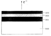
また、MIM型の例としては、たとえば、C.A.Mead,“Operation of tunnel-emission Devices”,J.Appl.Phys.,32,646(1961)などが知られている。MIM型の素子構成の典型的な例を図21に示す。同図は断面図であり、図において、3020は基板で、3021は金属よりなる下電極、3022は厚さ100Å程度の薄い絶縁層、3023は厚さ80〜300Å程度の金属よりなる上電極である。
【0011】
MIM型においては、上電極3023と下電極3021の間に適宜の電圧を印加することにより、上電極3023の表面より電子放出を起こさせるものである。
【0012】
上述の冷陰極素子は、熱陰極素子と比較して低温で電子放出を得ることができるため、加熱用ヒーターを必要としない。したがって、熱陰極素子よりも構造が単純であり、微細な素子を作成可能である。また、基板上に多数の素子を高い密度で配置しても、基板の熱溶融などの問題が発生しにくい。また、熱陰極素子がヒーターの加熱により動作するため応答速度が遅いのとは異なり、冷陰極素子の場合には応答速度が速いという利点もある。
【0013】
このため、冷陰極素子を応用するための研究が盛んに行われてきている。
【0014】
たとえば、表面伝導型放出素子は、冷陰極素子のなかでも特に構造が単純で製造も容易であることから、大面積にわたり多数の素子を形成できる利点がある。そこで、たとえば本出願人による特開昭64−31332号公報において開示されるように、多数の素子を配列して駆動するための方法が研究されている。
【0015】
また、表面伝導型放出素子の応用については、たとえば、画像表示装置、画像記録装置などの画像形成装置や、荷電ビーム源、等が研究されている。
【0016】
特に、画像表示装置への応用としては、たとえば本出願人による米国特許第5,066,883号や特開平2−257551号公報や特開平4−28137号公報において開示されているように、表面伝導型放出素子と電子ビームの照射により発光する蛍光体とを組み合わせて用いた画像表示装置が研究されている。表面伝導型放出素子と蛍光体とを組み合わせて用いた画像表示装置は、従来の他の方式の画像表示装置よりも優れた特性が期待されている。たとえば、近年普及してきた液晶表示装置と比較しても、自発光型であるためバックライトを必要としない点や、視野角が広い点が優れていると言える。
【0017】
また、FE型を多数個ならべて駆動する方法は、たとえば本出願人による米国特許第4,904,895号に開示されている。また、FE型を画像表示装置に応用した例として、たとえば、R.Meyerらにより報告された平板型表示装置が知られている[R.Meyer:“Recent Development on Microtips Display at LETI”,Tech.Digest of 4th Int.Vacuum Microele-ctronics Conf.,Nagahama,pp.6〜9(1991)]。
【0018】
また、MIM型を多数個並べて画像表示装置に応用した例は、たとえば本出願人による特開平3−55738号公報に開示されている。
【0019】
上記のような電子放出素子を用いた画像形成装置のうちで、奥行きの薄い平面型表示装置は省スペースかつ軽量であることから、ブラウン管型の表示装置に置き換わるものとして注目されている。
【0020】
図22は平面型の画像表示装置をなす表示パネル部の一例を示す斜視図であり、内部構造を示すためにパネルの一部を切り欠いて示している。
【0021】
図中、3115はリアプレート、3116は側壁、3117はフェースプレートであり、リアプレート3115、側壁3116およびフェースプレート3117により、表示パネルの内部を真空に維持するための外囲器(気密容器)を形成している。
【0022】
リアプレート3115には基板3111が固定されているが、この基板3111上には冷陰極素子3112が、N×M個形成されている。N、Mは2以上の正の整数であり、目的とする表示画素数に応じて適宜設定される。また、前記N×M個の冷陰極素子3112は、図22に示すとおり、M本の行方向配線3113とN本の列方向配線3114により配線されている。これら基板3111、冷陰極素子3112、行方向配線3113および列方向配線3114によって構成される部分をマルチ電子ビーム源と呼ぶ。また、行方向配線3113と列方向配線3114の少なくとも交差する部分には、両配線間に絶縁層(不図示)が形成されており、電気的な絶縁が保たれている。
【0023】
フェースプレート3117の下面には、蛍光体からなる蛍光膜3118が形成されており、赤(R)、緑(G)、青(B)の3原色の蛍光体(不図示)が塗り分けられている。また、蛍光膜3118をなす上記各色蛍光体の間には黒色体(不図示)が設けてあり、さらに蛍光膜3118のリアプレート3115側の面には、Al等からなるメタルバック3119が形成されている。
【0024】
Dx1〜DxmおよびDy1〜DynおよびHvは、当該表示パネルと不図示の電気回路とを電気的に接続するために設けた気密構造の電気接続用端子である。Dx1〜Dxmはマルチ電子ビーム源の行方向配線3113と、Dy1〜Dynはマルチ電子ビーム源の列方向配線3114と、Hvはメタルバック3119と各々電気的に接続している。
【0025】
また、上記気密容器の内部は10-6[Torr]程度の真空に保持されており、画像表示装置の表示面積が大きくなるにしたがい、気密容器内部と外部の気圧差によるリアプレート3115およびフェースプレート3117の変形あるいは破壊を防止する手段が必要となる。リアプレート3115およびフェースプレート3116を厚くすることによる方法は、画像表示装置の重量を増加させるのみならず、斜め方向から見たときに画像のゆがみや視差を生ずる。これに対し、図22においては、比較的薄いガラス板からなり大気圧を支えるための構造支持体(スペーサあるいはリブと呼ばれる)3120が設けられている。このようにして、マルチビーム電子源が形成された基板3111と蛍光膜3118が形成されたフェースプレート3116間は通常サブミリ乃至数ミリに保たれ、前述したように気密容器内部は高真空に保持されている。
【0026】
以上説明した表示パネルを用いた画像表示装置は、容器外端子Dx1乃至Dxm、Dy1乃至Dynを通じて各冷陰極素子3112に電圧を印加すると、各冷陰極素子3112から電子が放出される。それと同時にメタルバック3119に容器外端子Hvを通じて数百[V]乃至数[kV]の高圧を印加して、上記放出された電子を加速し、フェースプレート3117の内面に衝突させる。これにより、蛍光膜3118をなす各色の蛍光体が励起されて発光し、画像が表示される。
【0027】
【発明が解決しようとする課題】
以上述べた、画像形成装置等の電子線装置は、装置内部の真空雰囲気を維持するための外囲器、該外囲器内に配置された電子源、該電子源から放出された電子線が照射されるターゲット、電子線をターゲットに向けて加速するための加速電極等を有するが、さらに、外囲器に加わる大気圧を外囲気内部から支持するための支持部材(スペーサ)が外囲器内部に配置されることがある。
【0028】
このような画像表示装置の表示パネルにおいては、以下のような問題点があった。
【0029】
まず、スペーサの近傍から放出された電子の一部がスペーサに当たることにより、あるいは放出電子の作用でイオン化したイオンがスペーサに付着することにより、スペーサ帯電をひきおこす可能性がある。更には、フェースプレートに到達した電子が一部反射、散乱され、その一部がスペーサに当たることによりスペーサ帯電をひきおこす可能性がある。このスペーサの帯電により冷陰極素子から放出された電子はその軌道を曲げられ、蛍光体上の正規な位置とは異なる場所に到達し、スペーサ近傍の画像がゆがんで表示される。
【0030】
この問題点を解決するために、スペーサに微小電流が流れるようにして帯電を除去(以下除電)する提案がなされている。そこでは絶縁性のスペーサの表面に高抵抗層として高抵抗膜を形成することにより、スペーサ表面に微小電流が流れるようにしている。
しかしながら、高抵抗層には、画像形成装置組立時の熱工程において膜剥がれ等が生じるといった機械的安定性の問題や、表面酸化による状態変化やスペーサ材料の含有物質(例えばアルカリ元素)の拡散による化学的ダメージが発生するという問題があり、しばしば特性劣化の問題を生じていた。
【0031】
本発明は、表面の高抵抗層が機械的にも化学的にも安定したスペーサを有する電子線装置を提供することを目的とする。
【0032】
【課題を解決するための手段】
本発明者らは鋭意検討の結果、上述問題点の対策として、電子源基板、フェースプレート基板のうち少なくとも一方が熱膨張係数が80×10-7/℃から90×10-7/℃の間の値を持ちスペーサが75×10-7/℃から95×10-7/℃の熱膨張係数を有するセラミックス材料を用いることが有効であることを見出した。また、これらの熱膨張係数を有するセラミックスはアルミナにジルコニアを添加した混合焼成物材料で実現できることを見出した。このとき、アルミナと酸化ジルコニアの重量混合比は、70:30〜10:90の間とすることで所望の熱膨張係数が得られる。
【0033】
また、スペーサ基板がアルカリまたはアルカリ土類の金属の含有量が0.1%以下であることにより高抵抗膜への影響を防ぐことができる。
【0034】
さらに、高抵抗層を該スペーサ組立時の温度よりも、高い温度で予め処理することにより、組立時等それ以降の工程において高い安定性の高抵抗膜を形成することが可能となった。
【0035】
セラミックスは一般にガラスより耐熱性が高い。これは、高抵抗形成時あるいはその後の熱処理時において、セラミックスをスペーサ基板として用いることにより高温化処理を可能とし、熱的安定性、化学的安定性、剥がれ等の起こりにくい機械強度に優れる安定な高抵抗膜を形成することが可能となった。
【0036】
また、本発明の構成によりアルカリ元素を添加しないで熱膨張係数の調整が可能である。これは、高抵抗層の劣化を防ぐとともにアルカリ拡散によるスペーサの上下の接続部の不良を防ぐことが可能になった。
【0037】
本発明は上記従来スペーサの欠点を改善するものであり、寿命特性に優れた高い除電特性を示すスペーサを提供するものである。
【0038】
本発明の電子線装置は、以下のような形態を有するものであってもよい。
【0039】
▲1▼前記電子線装置は、前記電極が前記電子源より放出された電子を加速する加速電極であり、入力信号に応じて前記冷陰極素子から放出された電子を前記ターゲットに照射して画像を形成する画像形成装置をなす。特に、前記ターゲットが蛍光体である画像表示装置をなす。
【0040】
▲2▼前記冷陰極素子は、電子放出部を含む導電性膜を一対の電極間に有する冷陰極素子であり、特に好ましくは表面伝導型放出素子である。
【0041】
▲3▼前記電子源は、複数の行方向配線と複数の列方向配線とでマトリクス配線された複数の冷陰極素子を有する単純マトリクス状配置の電子源をなす。
【0042】
▲4▼前記電子源は、並列に配置した複数の冷陰極素子の個々を両端で接続した冷陰極素子の行を複数配し(行方向と呼ぶ)、この配線と直交する方向(列方向と呼ぶ)に沿って、冷陰極素子の上方に配した制御電極(グリッドとも呼ぶ)により、冷陰極素子からの電子を制御するはしご状配置の電子源をなす。
【0043】
▲5▼また、本発明の思想によれば、表示用として好適な画像形成装置に限るものではなく、感光性ドラムと発光ダイオード等で構成された光プリンタの発光ダイオード等の代替の発光源として、上述の画像形成装置を用いることもできる。またこの際、上述のm本の行方向配線とn本の列方向配線を、適宜選択することで、ライン状発光源だけでなく、2次元状の発光源としても応用できる。この場合、画像形成部材としては、以下の実施形態で用いる蛍光体のような直接発光する物質に限るものではなく、電子の帯電による潜像画像が形成されるような部材を用いることもできる。
【0044】
また、本発明の思想によれば、例えば電子顕微鏡のように、電子源からの放出電子の被照射部材が、蛍光体等の画像形成部材以外のものである場合についても、本発明は適用できる。従って、本発明は被照射部材を特定しない一般的電子線装置としての形態もとりうる。
【0045】
【発明の実施の形態】
次に、本発明を適用した画像表示装置の表示パネルの構成と製造法について、具体的な例を示して説明する。
【0046】
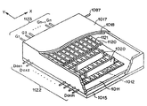
図1は、本実施形態に用いた表示パネルの斜視図であり、内部構造を示すためにパネルの一部を切り欠いて示している。
【0047】
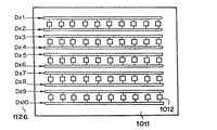
図中、1015はリアプレート、1016は側壁、1017はフェースプレートであり、1015〜1017により表示パネルの内部を真空に維持するための気密容器を形成している。気密容器を組み立てるにあたっては、各部材の接合部に十分な強度と気密性を保持させるため封着する必要があるが、たとえばフリットガラスを接合部に塗布し、大気中あるいは窒素雰囲気中で、摂氏400〜500度で10分以上焼成することにより封着を達成した。気密容器内部を真空に排気する方法については後述する。また、上記気密容器の内部は10-6[Torr]程度の真空に保持されるので、大気圧や不意の衝撃などによる気密容器の破壊を防止する目的で、耐大気圧構造体として、スペーサ1020が設けられている。リアプレート1015には、基板1011が固定されているが、該基板上には冷陰極素子1012がN×M個形成されている。N,Mは2以上の正の整数であり、目的とする表示画素数に応じて適宜設定される。たとえば、高品位テレビジョンの表示を目的とした表示装置においては、N=3000,M=1000以上の数を設定することが望ましい。前記N×M個の冷陰極素子は、M本の行方向配線1013とN本の列方向配線1014により単純マトリクス配線されている。前記、1011〜1014によって構成される部分をマルチ電子ビーム源と呼ぶ。
【0048】
本発明の画像表示装置に用いるマルチ電子ビーム源は、冷陰極素子を単純マトリクス配線した電子源であれば、冷陰極素子の材料や形状あるいは製法に制限はない。したがって、たとえば表面伝導型放出素子やFE型、あるいはMIM型などの冷陰極素子を用いることができる。
【0049】
次に、冷陰極素子として表面伝導型放出素子(後述)を基板上に配列して単純マトリクス配線したマルチ電子ビーム源の構造について述べる。
【0050】
図6に示すのは、図1の表示パネルに用いたマルチ電子ビーム源の平面図である。基板1011上には、後述の図4で示すものと同様な表面伝導型放出素子が配列され、これらの素子は行方向配線電極1003と列方向配線電極1004により単純マトリクス状に配線されている。行方向配線電極1013と列方向配線電極1014の交差する部分には、電極間に絶縁層(不図示)が形成されており、電気的な絶縁が保たれている。
【0051】
図6のB−B′に沿った断面を、図5に示す。
【0052】
なお、このような構造のマルチ電子源は、あらかじめ基板上に行方向配線電極1013、列方向配線電極1014、電極間絶縁層(不図示)、および表面伝導型放出素子の素子電極1102、1103と導電性薄膜1104を形成した後、行方向配線電極1013および列方向配線電極1014を介して各素子に給電して通電フォーミング処理(後述)と通電活性化処理(後述)を行うことにより製造した。
【0053】
本実施形態においては、気密容器のリアプレート1015にマルチ電子ビーム源の基板1011を固定する構成としたが、マルチ電子ビーム源の基板1011が十分な強度を有するものである場合には、気密容器のリアプレートとしてマルチ電子ビーム源の基板1011自体を用いてもよい。
【0054】
また、フェースプレート1017の下面には、蛍光膜1018が形成されている。本実施形態はカラー表示装置であるため、蛍光膜1018の部分にはCRTの分野で用いられる赤、緑、青、の3原色の蛍光体が塗り分けられている。各色の蛍光体は、たとえば図17(a)に示すようにストライプ状に塗り分けられ、蛍光体のストライプの間には黒色の導電体1010が設けてある。黒色の導電体1010を設ける目的は、電子ビームの照射位置に多少のずれがあっても表示色にずれが生じないようにする事や、外光の反射を防止して表示コストラストの低下を防ぐ事、電子ビームによる蛍光膜のチャージアップを防止する事などである。黒色の導電体1010には、黒鉛を主成分として用いたが、上記の目的に適するものであればこれ以外の材料を用いても良い。
【0055】
また、3原色の蛍光体の塗り分け方は前記図17(a)に示したストライプ状の配列に限られるものではなく、たとえば図17(b)に示すようなデルタ状配列や、それ以外の配列であってもよい。
【0056】
なお、モノクロームの表示パネルを作成する場合には、単色の蛍光体材料を蛍光膜1018に用いればよく、また黒色導電材料は必ずしも用いなくともよい。
【0057】
また、蛍光膜1018のリアプレート側の面には、CRTの分野では公知のメタルバック1019を設けてある。メタルバック1019を設けた目的は、蛍光膜1018が発する光の一部を鏡面反射して光利用率を向上させる事や、負イオンの衝突から蛍光膜1018を保護する事や、電子ビーム加速電圧を印加するための電極として作用させる事や、蛍光膜1018を励起した電子の導電路として作用させる事などである。メタルバック1019は、蛍光膜1018をフェースプレート基板1017上に形成した後、蛍光膜表面を平滑化処理し、その上にAlを真空蒸着する方法により形成した。なお、蛍光膜1018に低電圧用の蛍光体材料を用いた場合には、メタルバック1019は用いなくてもよい。
【0058】
また、本実施形態では用いなかったが、加速電圧の印加用や蛍光膜の導電性向上を目的として、フェースプレート基板1017と蛍光膜1018との間に、たとえばITOを材料とする透明電極を設けてもよい。
【0059】
図2は図1のA−A′の断面模式図であり、各部の番号は図1に対応している。スペーサ1020は絶縁性部材1の表面に帯電防止を目的とした第一の層である高抵抗膜11を有する。かつフェースプレート1017の内側(メタルバック1019等)及び基板1011の表面(行方向配線1013または列方向配線1014)に面したスペーサの当接面及び側面の一部に低抵抗膜3a、3bを有する。
【0060】
スペーサは、上記目的を達成するのに必要な数だけ、かつ必要な間隔をおいて配置され、フェースプレートの内側および基板1011の表面に接合材1041により固定される。
【0061】
また、高抵抗膜11は、絶縁性部材1の表面のうち、少なくとも気密容器内の真空中に露出している面に成膜されており、スペーサ1020上の低抵抗膜3a、3b、5a、5bおよび接合材1041を介して、フェースプレート1017の内側(メタルバック1019等)及び基板1011の表面(行方向配線1013または列方向配線1014)に電気的に接続される。ここで説明される形態においては、スペーサ1020の形状は薄板状とし、スペーサ1020は行方向配線1013に平行に配置され、行方向配線1013に電気的に接続されている。
【0062】
スペーサ基板1としては、基板1011上の行方向配線1013および列方向配線1014とフェースプレート1017内面のメタルバック1019との間に印加される高電圧に耐えるだけの電気的耐性を有し、スペーサ基板1の表面への帯電を防止する程度の導電性を有する必要がある。スペーサ基板1としては絶縁性部材が好ましくその熱膨張率が気密容器および基板1011を成す部材と近いものが好ましい。
【0063】
スペーサ1020を構成する高抵抗膜11には、高電位側のフェースプレート1017(メタルバック1019等)に印加される加速電圧Vaを帯電防止膜である高抵抗膜11の抵抗値Rsで除した電流が流される。そこで、スペーサの抵抗値Rsは帯電防止および消費電力からその望ましい範囲に設定される。帯電防止の観点から面積抵抗(sheet resistivity)R/□は1012Ω/□以下であることが好ましい。十分な帯電防止効果を得るためには1011Ω/□以下がさらに好ましい。面積抵抗の下限はスペーサ形状とスペーサ間に印加される電圧により左右されるが、105Ω/□以上であることが好ましい。
【0064】
絶縁材料上に形成された帯電防止膜の厚みtは10nm〜1μmの範囲が望ましい。材料の表面エネルギーおよび基板との密着性や基板温度によっても異なるが、一般的に10nm以下の薄膜は島状に形成され、抵抗が不安定で再現性に乏しい。一方、膜厚tが1μm以上では膜応力が大きくなって膜はがれの危険性が高まり、かつ成膜時間が長くなるため生産性が悪い。従って、膜厚は50〜500nmであることが望ましい。
【0065】
面積抵抗R/□はρ/tであり、以上に述べた面積抵抗R/□と膜厚tの好ましい範囲から、帯電防止膜の比抵抗ρは0.1[Ωcm]乃至108[Ωcm]が好ましい。さらに面積抵抗と膜厚のより好まし範囲を実現するためには、ρは102乃至106Ωcmとするのが良い。スペーサは上述したようにその上に形成した帯電防止膜を電流が流れることにより、あるいはディスプレイ全体が動作中に発熱することによりその温度が上昇する。帯電防止膜の抵抗温度係数が大きな負の値であると温度が上昇した時に抵抗値が減少し、スペーサに流れる電流が増加し、さらに温度上昇をもたらす。そして電流は電源の限界を越えるまで増加しつづける。このような電流の暴走が発生する抵抗温度係数の値は経験的に負の値で絶対値が1%以上である。すなわち、帯電防止膜の抵抗温度係数は−1%未満であることが望ましい。
【0066】
帯電防止特性を有する高抵抗膜11の材料としては、例えば酸化錫、酸化ニッケル等の金属酸化物を用いることが出来る。
【0067】
帯電防止特性を有する高抵抗膜11の他の材料として、アルミと遷移金属合金の窒化物は遷移金属の組成を調整することにより、良伝導体から絶縁体まで広い範囲で抵抗値を制御できるので好適な材料である。さらには後述する表示装置の作製工程において抵抗値の変化が少なく安定な材料である。かつ、その抵抗温度係数が−1%未満であり、実用的に使いやすい材料である。遷移金属元素としてはTi,Cr,Ta等があげられる。
【0068】
合金窒化膜はスパッタ、窒素ガス雰囲気中での反応性スパッタ、電子ビーム蒸着、イオンプレーティング、イオンアシスト蒸着法等の薄膜形成手段により絶縁性部材上に形成される。金属酸化膜も同様の薄膜形成法で作製することができるが、この場合窒素ガスに代えて酸素ガスを使用する。その他、CVD法、アルコキシド塗布法でも金属酸化膜を形成できる。カーボン膜は蒸着法、スパッタ法、CVD法、プラズマCVD法で作製され、特に非晶質カーボンを作製する場合には、成膜中の雰囲気に水素が含まれるようにするか、成膜ガスに炭化水素ガスを使用する。
【0069】
スペーサ1020を構成する低抵抗膜3a、3bは、高抵抗膜11を高電位側のフェースプレート1017(メタルバック1019等)及び低電位側の基板1011(配線1013、1014等)と電気的に接続する為に設けられたものであり、以下では、中間電極層(中間層)という名称も用いる。中間電極層(中間層)は以下に列挙する複数の機能を有することが出来る。
【0070】
▲1▼ 高抵抗膜11をフェースプレート1017及び基板1011と電気的に接続する。
【0071】
既に説明したように、高抵抗膜11はスペーサ1020表面での帯電を防止する目的で設けられたものであるが、高抵抗膜11をフェースプレート1017(メタルバック1019等)及び基板1011(配線1013、1014等)と直接或いは接合材1041を介して接続した場合、接続部界面に大きな接触抵抗が発生し、スペーサ表面に発生した電荷を速やかに除去できなくなる可能性がある。これを避ける為に、フェースプレート1017、基板1011及び接合材1041と接触するスペーサ1020の当接面或いは側面部に低抵抗の中間層を設けた。
【0072】
▲2▼ 高抵抗膜11の電位分布を均一化する。
【0073】
冷陰極素子1012より放出された電子は、フェースプレート1017と基板1011の間に形成された電位分布に従って電子軌道を成す。スペーサ1020の近傍で電子軌道に乱れが生じないようにする為には、高抵抗膜11の電位分布を全域にわたって制御する必要がある。高抵抗膜11をフェースプレート1017(メタルバック1019等)及び基板1011(配線1013、1014等)と直接或いは接合材1041を介して接続した場合、接続部界面の接触抵抗の為に、接続状態のむらが発生し、高抵抗膜11の電位分布が所望の値からずれてしまう可能性がある。これを避ける為に、スペーサ1020がフェースプレート1017及び基板1011と当接するスペーサ端部(当接面3或いは側面部5)の全長域に低抵抗の中間層を設け、この中間層部に所望の電位を印加することによって、高抵抗膜11全体の電位を制御可能とした。
【0074】
▲3▼ 放出電子の軌道を制御する。
【0075】
冷陰極素子1012より放出された電子は、フェースプレート1017と基板1011の間に形成された電位分布に従って電子軌道を成す。スペーサ近傍の冷陰極素子から放出された電子に関しては、スペーサを設置することに伴う制約(配線、素子位置の変更等)が生じる場合がある。このような場合、歪みやむらの無い画像を形成する為には、放出された電子の軌道を制御してフェースプレート1017上の所望の位置に電子を照射する必要がある。フェースプレート1017及び基板1011と当接する面の側面部5に低抵抗の中間層を設けることにより、スペーサ1020近傍の電位分布に所望の特性を持たせ、放出された電子の軌道を制御することが出来る。
【0076】
低抵抗膜3a、3bは、高抵抗膜11に比べ十分に低い抵抗値を有する材料を選択すればよく、Ni,Cr,Au,Mo,W,Pt,Ti,Al,Cu,Pd等の金属、あるいは合金、及びPd,Ag,Au,RuO2 ,Pd−Ag等の金属や金属酸化物とガラス等から構成される印刷導体、あるいはIn2 O3 −SnO2 等の透明導体及びポリシリコン等の半導体材料等より適宜選択される。
【0077】
導電性を有する接合材1041はスペーサ1020が行方向配線1013およびメタルバック1019と電気的に接続するように、導電性をもたせる必要がある。すなわち、導電性接着材や金属粒子や導電性フィラーを添加したフリットガラスが好適である。
【0078】
また、図1において、Dx1〜DxmおよびDy1〜DynおよびHvは、当該表示パネルと不図示の電気回路とを電気的に接続するために設けた気密構造の電気接続用端子である。Dx1〜Dxmはマルチ電子ビーム源の行方向配線1013と、Dy1〜Dynはマルチ電子ビーム源の列方向配線1014と、Hvはフェースプレートのメタルバック1019と電気的に接続している。
【0079】
また、気密容器内部を真空に排気するには、気密容器を組み立てた後、不図示の排気管と真空ポンプとを接続し、気密容器内を10-7[Torr]程度の真空度まで排気する。その後、排気管を封止するが、気密容器内の真空度を維持するために、封止の直前あるいは封止後に気密容器内の所定の位置にゲッター膜(不図示)を形成する。ゲッター膜とは、たとえばBaを主成分とするゲッター材料をヒーターもしくは高周波加熱により加熱し蒸着して形成した膜であり、該ゲッター膜の吸着作用により気密容器内は1×10⁻⁵乃至1×10⁻⁷[Torr]の真空度に維持される。
【0080】
以上説明した表示パネルを用いた画像表示装置は、容器外端子Dx1乃至Dxm、Dy1乃至Dynを通じて各冷陰極素子1012に電圧を印加すると、各冷陰極素子1012から電子が放出される。それと同時にメタルバック1019に容器外端子Hvを通じて数百[V]乃至数[kV]の高圧を印加して、上記放出された電子を加速し、フェースプレート1017の内面に衝突させる。これにより、蛍光膜1018をなす各色の蛍光体が励起されて発光し、画像が表示される。
【0081】
通常、冷陰極素子である本発明の表面伝導型放出素子1012への印加電圧は12〜16[V]程度、メタルバック1019と冷陰極素子1012との距離dは0.1[mm]から8[mm]程度、メタルバック1019と冷陰極素子1012間の電圧0.1[kV]から10[kV]程度である。
【0082】
以上、本発明の実施形態の表示パネルの基本構成と製法、および画像表示装置の概要を説明した。
【0083】
次に、前記実施形態の表示パネルに用いたマルチ電子ビーム源の製造方法について説明する。本発明の画像表示装置に用いるマルチ電子ビーム源は、冷陰極素子を単純マトリクス配線した電子源であれば、冷陰極素子の材料や形状あるいは製法に制限はない。したがって、たとえば表面伝導型放出素子やFE型、あるいはMIM型などの冷陰極素子を用いることができる。
【0084】
ただし、表示画面が大きくてしかも安価な表示装置が求められる状況のもとでは、これらの冷陰極素子の中でも、表示伝導型放出素子が特に好ましい。すなわち、FE型ではエミッタコーンとゲート電極の相対位置や形状が電子放出特性を大きく左右するため、極めて高精度の製造技術を必要とするが、これは大面積化や製造コストの低減を達成するには不利な要因となる。また、MIM型では、絶縁層と上電極の膜厚を薄くてしかも均一にする必要があるが、これも大面積化や製造コストの低減を達成するには不利な要因となる。その点、表面伝導型放出素子は、比較的製造方法が単純なため、大面積化や製造コストの低減が容易である。また、発明者らは、表面伝導型放出素子の中でも、電子放出部もしくはその周辺部を微粒子膜から形成したものがとりわけ電子放出特性に優れ、しかも製造が容易に行えることを見いだしている。したがって、高輝度で大画面の画像表示装置のマルチ電子ビーム源に用いるには、最も好適であると言える。そこで、上記実施形態の表示パネルにおいては、電子放出部もしくはその周辺部を微粒子膜から形成した表面伝導型放出素子を用いた。そこで、まず好適な表面伝導型放出素子について基本的な構成と製法および特性を説明し、その後で多数の素子を単純マトリクス配線したマルチ電子ビーム源の構造について述べる。
【0085】
[表面伝導型放出素子の好適な素子構成と製法]
電子放出部もしくはその周辺部を微粒子膜から形成する表面伝導型放出素子の代表的な構成には、平面型と垂直型の2種類があげられる。
【0086】
[平面型の表面伝導型放出素子]
まず最初に、平面型の表面伝導型放出素子の素子構成と製法について説明する。
【0087】
図4に示すのは、平面型の表面伝導型放出素子の構成を説明するための平面図(a)および断面図(b)である。図中、1011は基板、1102と1103は素子電極、1104は導電性薄膜、1105は通電フォーミング処理により形成した電子放出部、1113は通電活性化処理により形成した薄膜である。
【0088】
また、基板1011上に基板面と平行に対向して設けられた素子電極1102と1103は、導電性を有する材料によって形成されている。たとえば、Ni,Cr,Au,Mo,W,Pt,Ti,Cu,Pd,Ag等をはじめとする金属、あるいはこれらの金属の合金、あるいはIn2 O3 −SnO2 をはじめとする金属酸化物、ポリシリコンなどの半導体、などの中から適宜材料を選択して用いればよい。電極を形成するには、たとえば真空蒸着などの製膜技術とフォトリソグラフィー、エッチングなどのパターニング技術を組み合わせて用いれば容易に形成できるが、それ以外の方法(たとえば印刷技術)を用いて形成してもさしつかえない。
【0089】
素子電極1102と1103の形状は、当該電子放出素子の応用目的に合わせて適宜設計される。一般的には、電極間隔Lは通常は数百Åから数百μmの範囲から適当な数値を選んで設計されるが、なかでも表示装置に応用するために好ましいのは数μmより数十μmの範囲である。また、素子電極の厚さdについては、通常は数百Åから数μmの範囲から適当な数値が選ばれる。
【0090】
また、導電性薄膜1104の部分には、微粒子膜を用いる。ここで述べた微粒子膜とは、構成要素として多数の微粒子を含んだ膜(島状の集合体も含む)のことをさす。微粒子膜を微視的に調べれば、通常は、個々の微粒子が離間して配置された構造か、あるいは微粒子が互いに隣接した構造か、あるいは微粒子が互いに重なり合った構造が観測される。
【0091】
微粒子膜に用いた微粒子の粒径は、数Åから数千Åの範囲に含まれるものであるが、なかでも好ましいのは10Åから200Åの範囲のものである。また、微粒子膜の膜厚は、以下に述べるような諸条件を考慮して適宜設定される。すなわち、素子電極1102あるいは1103と電気的に良好に接続するのに必要な条件、後述する通電フォーミングを良好に行うのに必要な条件、微粒子膜自身の電気抵抗を後述する適宜の値にするために必要な条件、などである。具体的には、数Åから数千Åの範囲のなかで設定するが、なかでも好ましいのは10Åから500Åの間である。
【0092】
また、微粒子膜を形成するのに用いられうる材料としては、たとえば、Pd,Pt,Ru,Ag,Au,Ti,In,Cu,Cr,Fe,Zn,Sn,Ta,W,Pb,などをはじめとする金属や、PdO,SnO2 ,In2 O3 ,PbO,Sb2 O3 ,などをはじめとする酸化物や、HfB2 ,ZrB2 ,LaB6 ,CeB6 ,YB4 ,GdB4 ,などをはじめとする硼化物や、TiC,ZrC,HfC,TaC,SiC,WC,などをはじめとする炭化物や、TiN,ZrN,HfN,などをはじめとする窒化物や、Si,Ge,などをはじめとする半導体や、カーボン、などがあげられ、これらの中から適宜選択される。
【0093】
以上述べたように、導電性薄膜1104を微粒子膜で形成したが、その面積抵抗値については、103から107[オーム/□]の範囲に含まれるよう設定した。
【0094】
なお、導電性薄膜1104と素子電極1102および1103とは、電気的に良好に接続されるのが望ましいため、互いの一部が重なりあうような構造をとっている。その重なり方は、図4の例においては、下から、基板、素子電極、導電性薄膜の順序で積層したが、場合によっては下から基板、導電性薄膜、素子電極、の順序で積層してもさしつかえない。
【0095】
また、電子放出部1105は、導電性薄膜1104の一部に形成された亀裂状の部分であり、電気的には周囲の導電性薄膜よりも高抵抗な性質を有している。亀裂は、導電性薄膜1104に対して、後述する通電フォーミングの処理を行うことにより形成する。亀裂内には、数Åから数百Åの粒径の微粒子を配置する場合がある。なお、実際の電子放出部の位置や形状を精密かつ正確に図示するのは困難なため、図4においては模式的に示した。
【0096】
また、薄膜1113は、炭素もしくは炭素化合物よりなる薄膜で、電子放出部1105およびその近傍を被覆している。薄膜1113は、通電フォーミング処理後に、後述する通電活性化の処理を行うことにより形成する。
【0097】
薄膜1113は、単結晶グラファイト、多結晶グラファイト、非晶質カーボン、のいずれかか、もしくはその混合物であり、膜厚は500[Å]以下とするが、300[Å]以下とするのがさらに好ましい。なお、実際の薄膜1113の位置や形状を精密に図示するのは困難なため、図4においては模式的に示した。また、平面図(a)においては、薄膜1113の一部(1105の上層部)を除去した素子を図示した。
【0098】
以上、好ましい素子の基本構成を述べたが、実施形態においては以下のような素子を用いた。
【0099】
すなわち、基板1011には青板ガラスを用い、素子電極1102と1103にはNi薄膜を用いた。素子電極の厚さdは1000[Å]、電極間隔Lは2[μm]とした。
【0100】
微粒子膜の主要材料としてPdもしくはPdOを用い、微粒子膜の厚さは約100[Å]、幅Wは100[μm]とした。
【0101】
次に、好適な平面型の表面伝導型放出素子の製造方法について説明する。
【0102】
図9の(a)〜(e)は、表面伝導型放出素子の製造工程を説明するための断面図で、各部材の表記は前記図4と同一である。
【0103】
1)まず、図9(a)に示すように、基板1011上に素子電極1102および1103を形成する。
【0104】
形成するにあたっては、あらかじめ基板1011を洗剤、純水、有機溶剤を用いて十分に洗浄後、素子電極の材料を堆積させる。(堆積する方法としては、たとえば、蒸着法やスパッタ法などの真空成膜技術を用ればよい。)その後、堆積した電極材料を、フォトリソグラフィー・エッチング技術を用いてパターニングし、(a)に示した一対の素子電極(1102と1103)を形成する。
【0105】
2)次に、同図(b)に示すように、導電性薄膜1104を形成する。
【0106】
形成するにあたっては、まず前記(a)の基板に有機金属溶液を塗布して乾燥し、加熱焼成処理して微粒子膜を成膜した後、フォトリソグラフィー・エッチングにより所定の形状にパターニングする。ここで、有機金属溶液とは、導電性薄膜に用いる微粒子の材料を主要元素とする有機金属化合物の溶液である。(具体的には、本実施形態では主要元素としてPdを用いた。また、本実施形態では塗布方法として、ディッピング法を用いたが、それ以外のたとえばスピンナー法やスプレー法を用いてもよい。)
また、微粒子膜で作られる導電性薄膜の成膜方法としては、本実施形態で用いた有機金属溶液の塗布による方法以外の、たとえば真空蒸着法やスパッタ法、あるいは化学的気相堆積法などを用いる場合もある。
【0107】
3)次に、同図(c)に示すように、フォーミング用電源1110から素子電極1102と1103の間に適宜の電圧を印加し、通電フォーミング処理を行って、電子放出部1105を形成する。
【0108】
通電フォーミング処理とは、微粒子膜で作られた導電性薄膜1104に通電を行って、その一部を適宜に破壊、変形、もしくは変質せしめ、電子放出を行うのに好適な構造に変化させる処理のことである。微粒子膜で作られた導電性薄膜のうち電子放出を行うのに好適な構造に変化した部分(すなわち電子放出部1105)においては、薄膜に適当な亀裂が形成されている。なお、電子放出部1105が形成される前と比較すると、形成された後は素子電極1102と1103の間で計測される電気抵抗は大幅に増加する。
【0109】
通電方法をより詳しく説明するために、図10に、フォーミング用電源1110から印加する適宜の電圧波形の一例を示す。微粒子膜で作られた導電性薄膜をフォーミングする場合には、パルス状の電圧が好ましく、本実施形態の場合には同図に示したようにパルス幅T1の三角波パルスをパルス間隔T2で連続的に印加した。その際には、三角波パルスの波高値Vpfを、順次昇圧した。また、電子放出部1105の形成状況をモニターするためのモニターパルスPmを適宜の間隔で三角波パルスの間に挿入し、その際に流れる電流を電流計1111で計測した。
【0110】
本実施形態においては、たとえば10-5[torr]程度の真空雰囲気下において、たとえばパルス幅T1を1[msec]、パルス間隔T2を10[msec]とし、波高値Vpfを1パルスごとに0.1[V]ずつ昇圧した。そして、三角波を5パルス印加するたびに1回の割りあいで、モニターパルスPmを挿入した。フォーミング処理に悪影響を及ぼすことがないように、モニターパルスの電圧Vpmは0.1[V]に設定した。そして、素子電極1102と1103の間の電気抵抗が1×10⁶[Ω]になった段階、すなわちモニターパルス印加時に電流計1111で計測される電流が1×10⁻⁷[A]以下になった段階で、フォーミング処理にかかわる通電を終了した。
【0111】
なお、上記の方法は、本実施形態の表面伝導型放出素子に関する好ましい方法であり、たとえば微粒子膜の材料や膜厚、あるいは素子電極間隔Lなど表面伝導型放出素子の設計を変更した場合には、それに応じて通電の条件を適宜変更するのが望ましい。
【0112】
4)次に、図9(d)に示すように、活性化用電源1112から素子電極1102と1103の間に適宜の電圧を印加し、通電活性化処理を行って、電子放出特性の改善を行う。
【0113】
通電活性化処理とは、前記通電フォーミング処理により形成された電子放出部1105に適宜の条件で通電を行って、その近傍に炭素もしくは炭素化合物を堆積せしめる処理のことである。(図においては、炭素もしくは炭素化合物よりなる堆積物を部材1113として模式的に示した。)なお、通電活性化処理を行うことにより、行う前と比較して、同じ印加電圧における放出電流を典型的には100倍以上に増加させることができる。
【0114】
具体的には、10-4乃至10-5[Torr]の範囲内の真空雰囲気中で、電圧パルスを定期的に印加することにより、真空雰囲気中に存在する有機化合物を起源とする炭素もしくは炭素化合物を堆積させる。堆積物1113は、単結晶グラファイト、多結晶グラファイト、非晶質カーボン、のいずれかか、もしくはその混合物であり、膜厚は500[Å]以下、より好ましくは300[Å]以下である。
【0115】
通電方法をより詳しく説明するために、図11(a)に、活性化用電源1112から印加する適宜の電圧波形の一例を示す。本実施形態においては、一定電圧の矩形波を定期的に印加して通電活性化処理を行ったが、具体的には、矩形波の電圧Vacは14[V],パルス幅T3は1[msec],パルス間隔T4は10[msec]とした。なお、上述の通電条件は、本実施形態の表面伝導型放出素子に関する好ましい条件であり、表面伝導型放出素子の設計を変更した場合には、それに応じて条件を適宜変更するのが望ましい。
【0116】
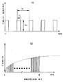
図9(d)に示す1114は該表面伝導型放出素子から放出される放出電流Ieを捕捉するためのアノード電極で、直流高電圧電源1115および電流計1116が接続されている。(なお、基板1011を、表示パネルの中に組み込んでから活性化処理を行う場合には、表示パネルの蛍光面をアノード電極1114として用いる。)活性化用電源1112から電圧を印加する間、電流計1116で放出電流Ieを計測して通電活性化処理の進行状況をモニターし、活性化用電源1112の動作を制御する。電流計1116で計測された放出電流Ieの一例を図11(b)に示すが、活性化電源1112からパルス電圧を印加しはじめると、時間の経過とともに放出電流Ieは増加するが、やがて飽和してほとんど増加しなくなる。このように、放出電流Ieがほぼ飽和した時点で活性化用電源1112からの電圧印加を停止し、通電活性化処理を終了する。
【0117】
なお、上述の通電条件は、本実施形態の表面伝導型放出素子に関する好ましい条件であり、表面伝導型放出素子の設計を変更した場合には、それに応じて条件を適宜変更するのが望ましい。
【0118】
以上のようにして、図9(e)に示す平面型の表面伝導型放出素子を製造した。
【0119】
[垂直型の表面伝導型放出素子]
次に、電子放出部もしくはその周辺を微粒子膜から形成した表面伝導型放出素子のもうひとつの代表的な構成、すなわち垂直型の表面伝導型放出素子の構成について説明する。
【0120】
図7は、垂直型の基本構成を説明するための模式的な断面図であり、図中の1201は基板、1202と1203は素子電極、1206は段差形成部材、1204は微粒子膜を用いた導電性薄膜、1205は通電フォーミング処理により形成した電子放出部、1213は通電活性化処理により形成した薄膜、である。
【0121】
垂直型が先に説明した平面型と異なる点は、素子電極のうちの片方(1202)が段差形成部材1206上に設けられており、導電性薄膜1204が段差形成部材1206の側面を被覆している点にある。したがって、前記図4の平面型における素子電極間隔Lは、垂直型においては段差形成部材1206の段差高Lsとして設定される。なお、基板1201、素子電極1202および1203、微粒子膜を用いた導電性薄膜1204、については、前記平面型の説明中に列挙した材料を同様に用いることが可能である。また、段差形成部材1206には、たとえばSiO2 のような電気的に絶縁性の材料を用いる。
【0122】
次に、垂直型の表面伝導型放出素子の製法について説明する。図12(a)〜(f)は、製造工程を説明するための断面図で、各部材の表記は前記図7と同一である。
【0123】
1)まず、図12(a)に示すように、基板1201上に素子電極1203を形成する。
【0124】
2)次に、同図(b)に示すように、段差形成部材を形成するための絶縁層を積層する。絶縁層は、たとえばSiO2 をスパッタ法で積層すればよいが、たとえば真空蒸着法や印刷法などの他の成膜方法を用いてもよい。
【0125】
3)次に、同図(c)に示すように、絶縁層の上に素子電極1202を形成する。
【0126】
4)次に、同図(d)に示すように、絶縁層の一部を、たとえばエッチング法を用いて除去し、素子電極1203を露出させる。
【0127】
5)次に、同図(e)に示すように、微粒子膜を用いた導電性薄膜1204を形成する。形成するには、前記平面型の場合と同じく、たとえば塗布法などの成膜技術を用いればよい。
【0128】
6)次に、前記平面型の場合と同じく、通電フォーミング処理を行い、電子放出部を形成する。(図9(c)を用いて説明した平面型の通電フォーミング処理と同様の処理を行えばよい。)
7)次に、前記平面型の場合と同じく、通電活性化処理を行い、電子放出部近傍に炭素もしくは炭素化合物を堆積させる。(図9(d)を用いて説明した平面型の通電活性化処理と同様の処理を行えばよい。)
以上のようにして、図12(f)に示す垂直型の表面伝導型放出素子を製造した。
【0129】
[表示装置に用いた表面伝導型放出素子の特性]
以上、平面型と垂直型の表面伝導型放出素子について素子構成と製法を説明したが、次に表示装置に用いた素子の特性について述べる。
【0130】
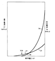
図8に、表示装置に用いた素子の、(放出電流Ie)対(素子印加電圧Vf)特性、および(素子電流If)対(素子印加電圧Vf)特性の典型的な例を示す。なお、放出電流Ieは素子電流Ifに比べて著しく小さく、同一尺度で図示するのが困難であるうえ、これらの特性は素子の大きさや形状等の設計パラメータを変更することにより変化するものであるため、2本の特性は各々任意単位で図示した。
【0131】
表示装置に用いた素子は、放出電流Ieに関して以下に述べる3つの特性を有している。
【0132】
第一に、ある電圧(これを閾値電圧Vthと呼ぶ)以上の大きさの電圧を素子に印加すると急激に放出電流Ieが増加するが、一方、閾値電圧Vth未満の電圧では放出電流Ieはほとんど検出されない。
【0133】
すなわち、放出電流Ieに関して、明確な閾値電圧Vthを持った非線形素子である。
【0134】
第二に、放出電流Ieは素子に印加する電圧Vfに依存して変化するため、電圧Vfで放出電流Ieの大きさを制御できる。
【0135】
第三に、素子に印加する電圧Vfに対して素子から放出される電流Ieの応答速度が速いため、電圧Vfを印加する時間の長さによって素子から放出される電子の電荷量を制御できる。
【0136】
以上のような特性を有するため、表面伝導型放出素子を表示装置に好適に用いることができた。たとえば多数の素子を表示画面の画素に対応して設けた表示装置において、第一の特性を利用すれば、表示画面を順次走査して表示を行うことが可能である。すなわち、駆動中の素子には所望の発光輝度に応じて閾値電圧Vth以上の電圧を適宜印加し、非選択状態の素子には閾値電圧Vth未満の電圧を印加する。駆動する素子を順次切り替えてゆくことにより、表示画面を順次走査して表示を行うことが可能である。
【0137】
また、第二の特性かまたは第三の特性を利用することにより、発光輝度を制御することができるため、階調表示を行うことが可能である。
【0138】
[多数素子を単純マトリクス配線したマルチ電子ビーム源の構造]
次に、上述の表面伝導型放出素子を基板上に配列して単純マトリクス配線したマルチ電子ビーム源の構造について述べる。
【0139】
図6に示すのは、前記図1の表示パネルに用いたマルチ電子ビーム源の平面図である。基板上には、前記図4で示したものと同様な表面伝導型放出素子が配列され、これらの素子は行方向配線電極1003と列方向配線電極1004により単純マトリクス状に配線されている。行方向配線電極1003と列方向配線電極1004の交差する部分には、電極間に絶縁層(不図示)が形成されており、電気的な絶縁が保たれている。
【0140】
図6のB−B′に沿った断面を、図5に示す。
【0141】
なお、このような構造のマルチ電子源は、あらかじめ基板上に行方向配線電極1013、列方向配線電極1014、電極間絶縁層(不図示)、および表面伝導型放出素子の素子電極と導電性薄膜を形成した後、行方向配線電極1013および列方向配線電極1014を介して上述したように各素子に給電して通電フォーミング処理と通電活性化処理を行うことにより製造した。
【0142】
図13は、NTSC方式のテレビ信号に基づいてテレビジョン表示を行う為の駆動回路の概略構成をブロック図で示したものである。同図中、表示パネル1701は前述した表示パネルに相当するもので、前述した様に製造され、動作する。また、走査回路1702は表示ラインを走査し、制御回路1703は走査回路へ入力する信号等を生成する。シフトレジスタ1704は1ライン毎のデータをシフトし、ラインメモリ1705は、シフトレジスタ1704からの1ライン分のデータを変調信号発生器1707に入力する。同期信号分離回路1706はNTSC信号から同期信号を分離する。
【0143】
以下、図13の装置各部の機能を詳しく説明する。
【0144】
まず表示パネル1701は、端子Dx1乃至Dxmおよび端子Dy1乃至Dyn、および高圧端子Hvを介して外部の電気回路と接続されている。このうち、端子Dx1乃至Dxmには、表示パネル1701内に設けられているマルチ電子ビーム源、すなわちm行n列の行列状にマトリクス配線された冷陰極素子を1行(n素子)ずつ順次駆動してゆく為の走査信号が印加される。一方、端子Dy1乃至Dynには、前記走査信号により選択された1行分のn個の各素子の出力電子ビームを制御する為の変調信号が印加される。また、高圧端子Hvには、直流電圧源Vaより、たとえば5[kV]の直流電圧が供給されるが、これはマルチ電子ビーム源より出力される電子ビームに蛍光体を励起するのに十分なエネルギーを付与する為の加速電圧である。
【0145】
次に、走査回路1702について説明する。同回路は、内部にm個のスイッチング素子(図中、S1乃至Smで模式的に示されている)を備えるもので、各スイッチング素子は、直流電圧源Vxの出力電圧もしくは0[V](グランドレベル)のいずれか一方を選択し、表示パネル1701の端子Dx1乃至Dxmと電気的に接続するものである。S1乃至Smの各スイッチング素子は、制御回路1703が出力する制御信号Tscanに基づいて動作するものだが、実際にはたとえばFETのようなスイッチング素子を組合わせる事により容易に構成することが可能である。なお、前記直流電圧源Vxは、図8に例示した電子放出素子の特性に基づき走査されていない素子に印加される駆動電圧が電子放出しきい値電圧Vth電圧以下となるよう、一定電圧を出力するよう設定されている。
【0146】
また、制御回路1703は、外部より入力する画像信号に基づいて適切な表示が行なわれるように各部の動作を整合させる働きをもつものである。次に説明する同期信号分離回路1706より送られる同期信号Tsyncに基づいて、各部に対してTscanおよびTsftおよびTmryの各制御信号を発生する。同期信号分離回路1706は、外部から入力されるNTSC方式のテレビ信号から、同期信号成分と輝度信号成分とを分離する為の回路である。同期信号分離回路1706により分離された同期信号は、良く知られるように垂直同期信号と水平同期信号より成るが、ここでは説明の便宜上、Tsync信号として図示した。一方、前記テレビ信号から分離された画像の輝度信号成分を便宜上DATA信号と表すが、同信号はシフトレジスタ1704に入力される。
【0147】
シフトレジスタ1704は、時系列的にシリアルに入力される前記DATA信号を、画像の1ライン毎にシリアル/パラレル変換するためのもので、前記制御回路1703より送られる制御信号Tsftに基づいて動作する。すなわち、制御信号Tsftは、シフトレジスタ1704のシフトクロックであると言い換えることもできる。シリアル/パラレル変換された画像1ライン分(電子放出素子n素子分の駆動データに相当する)のデータは、Id1乃至Idnのn個の信号として前記シフトレジスタ1704より出力される。
【0148】
ラインメモリ1705は、画像1ライン分のデータを必要時間の間だけ記憶する為の記憶装置であり、制御回路1703より送られる制御信号Tmryにしたがって適宜Id1乃至Idnの内容を記憶する。記憶された内容は、I′d1乃至I′dnとして出力され、変調信号発生器1707に入力される。
【0149】
変調信号発生器1707は、前記画像データI′d1乃至I′dnの各々に応じて、電子放出素子1012の各々を適切に駆動変調する為の信号源で、その出力信号は、端子Doy1乃至Doynを通じて表示パネル1701内の電子放出素子1012に印加される。
【0150】
図8を用いて説明したように、本発明に関わる表面伝導型放出素子は放出電流Ieに対して以下の基本特性を有している。すなわち、電子放出には明確な閾値電圧Vth(後述する実施例の表面伝導型放出素子では8[V])があり、閾値Vth以上の電圧を印加された時のみ電子放出が生じる。また、電子放出閾値以上の電圧に対しては、図8のグラフのように電圧の変化に応じて放出電流Ieも変化する。このことから、本素子にパルス状の電圧を印加する場合、たとえば電子放出閾値Vth以下の電圧を印加しても電子放出は生じないが、電子放出閾値Vth以上の電圧を印加する場合には表面伝導型放出素子から電子ビームが出力される。その際、パルスの波高値Vmを変化させることにより出力電子ビームの強度を制御することが可能である。また、パルスの幅Pwを変化させることにより出力される電子ビームの電荷の総量を制御することが可能である。
【0151】
従って、入力信号に応じて、電子放出素子を変調する方式としては、電圧変調方式、パルス幅変調方式等が採用できる。電圧変調方式を実施するに際しては、変調信号発生器1707として、一定長さの電圧パルスを発生し、入力されるデータに応じて適宜パルスの波高値を変調するような電圧変調方式の回路を用いることができる。また、パルス幅変調方式を実施するに際しては、変調信号発生器1707として、一定の波高値の電圧パルスを発生し、入力されるデータに応じて適宜電圧パルスの幅を変調するようなパルス幅変調方式の回路を用いることができる。
【0152】
シフトレジスタ1704やラインメモリ1705は、デジタル信号式のものでもアナログ信号式のものでも採用できる。すなわち、画像信号のシリアル/パラレル変換や記憶が所定の速度で行われればよいからである。
【0153】
デジタル信号式を用いる場合には、同期信号分離回路1706の出力信号DATAをデジタル信号化する必要があるが、これには同期信号分離回路1706の出力部にA/D変換器を設ければよい。これに関連してラインメモリ1705の出力信号がデジタル信号かアナログ信号かにより、変調信号発生器に用いられる回路が若干異なったものとなる。すなわち、デジタル信号を用いた電圧変調方式の場合、変調信号発生器1707には、例えばD/A変換回路を用い、必要に応じて増幅回路などを付加する。パルス幅変調方式の場合、変調信号発生器1707には、例えば高速の発振器および発振器の出力する波数を計数する計数器(カウンタ)および計数器の出力値と前記メモリの出力値を比較する比較器(コンパレータ)を組み合せた回路を用いる。必要に応じて、比較器の出力するパルス幅変調された変調信号を電子放出素子の駆動電圧にまで電圧増幅するための増幅器を付加することもできる。
【0154】
アナログ信号を用いた電圧変調方式の場合、変調信号発生器1707には、例えばオペアンプなどを用いた増幅回路を採用でき、必要に応じてシフトレベル回路などを付加することもできる。パルス幅変調方式の場合には、例えば、電圧制御型発振回路(VOC)を採用でき、必要に応じて電子放出素子の駆動電圧まで電圧増幅するための増幅器を付加することもできる。
【0155】
このような構成をとりうる本発明の適用可能な画像表示装置においては、各電子放出素子に、容器外端子Dox1乃至Doxm、Doy1乃至Doynを介して電圧を印加することにより、電子放出が生ずる。高圧端子Hvを介してメタルバック1019あるいは透明電極(不図示)に高圧を印加し、電子ビームを加速する。加速された電子は、蛍光膜1018に衝突し、発光が生じて画像が形成される。
【0156】
次に、前述のはしご型配置電子源基板およびそれを用いた画像表示装置について図14および図15を用いて説明する。
【0157】
図14において、1011は電子源基板、1012は電子放出素子、1126のDx1〜Dx10は前記電子放出素子に接続する共通配線である。電子放出素子1012は、基板1011上に、X方向に並列に複数個配置される(これを素子行と呼ぶ)。この素子行を複数個基板上に配置し、はしご型電子源基板となる。各素子行の共通配線間に適宜駆動電圧を印加することで、各素子行を独立に駆動することが可能になる。すなわち、電子ビームを放出させる素子行には、電子放出閾値以上の電圧の電子ビームを、放出させない素子行には電子放出閾値以下の電圧を印加すればよい。また、各素子行間の共通配線Dx2〜Dx9を、例えばDx2,Dx3を同一配線とするようにしてもよい。
【0158】
図15は、はしご型配置の電子源を備えた画像形成装置の構造を示す図である。1120はグリッド電極、1121は電子が通過するための空孔、1122はDox1,Dox2…Doxよりなる容器外端子、1123はグリッド電極1120と接続されたG1,G2…Gnからなる容器外端子、1011は前述のように各素子行間の共通配線を同一配線とした電子源基板である。なお、図14、図15と同一の符号は同一の部材を示す。前述の単純マトリクス配置の画像形成装置(図1)との違いは、電子源基板1011とフェースプレート1017の間にグリッド電極1120を備えていることである。
【0159】
前述のパネル構造は、電子源配置が、マトリクス配線或いははしご型配置のいずれの場合でも、大気圧構造上必要に応じて、フェースプレート1017とリアプレート1015の間にスペーサ120を設けることができる。
【0160】
基板1011とフェースプレート1017の中間には、グリッド電極1120が設けられている。グリッド電極1120は、表面伝導型電子放出素子1012から放出された電子ビームを変調することができるもので、はしご型配置の素子行と直交して設けられたストライプ状の電極に電子ビームを通過させるため、各素子に対応して1個ずつ円形の開口1121が設けられている。グリッドの形状や設置位置は必ずしも図15のようなものでなくともよく、開口としてメッシュ状に多数の通過口を設けることもあり、また例えば表面伝導型電子放出素子の周囲や近傍に設けてもよい。
【0161】
容器外端子1122およびグリッド容器外端子1123は、図13の駆動回路と電気的に接続されている。
【0162】
本画像形成装置では、素子行を1行(1ライン)ずつ順次駆動(走査)していくのと同期してグリッド電極列に画像1ライン分の変調信号を同時に印加することにより、各電子ビームの蛍光体への照射を制御し、画像を1ラインずつ表示することができる。
【0163】
上記の2つの画像表示装置の構成は、本発明を適用可能な画像形成装置の一例であり、本発明の思想に基づいて種々の変形が可能である。入力信号についてはNTSC方式を挙げたが、入力信号はこれに限るものではなく、PAL、SECAM方式など他、これらより多数の走査線からなるTV信号(高品位TV)方式をも採用できる。
【0164】
また、本発明によればテレビジョン放送の表示装置のみならずテレビ会議システム、コンピュータ等の表示装置に適した画像形成装置を提供することができる。さらには感光性ドラム等で構成された光プリンターとしての画像形成装置として用いることもできる。
【0165】
【実施例】
以下に実施例を挙げて、本発明の特徴であるスペーサの構成について、さらに説明を加える。
【0166】
以下に述べる各実施例においては、マルチ電子ビーム源として、前述した、電極間の導電性微粒子膜に電子放出部を有するタイプのN×M個(M=3072、M=1024)の表面伝導型放出素子を、M本の行方向配線とN本の列方向配線とによりマトリクス配線(図1および図6参照)したマルチ電子ビーム源を用いた。
【0167】
[実施例1]
本実施例では、前述した図1に示すスペーサ1020を配置した表示パネルを作製した。以下、図1および図2を用いて詳述する。まず、あらかじめ基板上に行方向配線電極1013、列方向配線電極1014、電極間絶縁層(不図示)、および表面伝導型放出素子1012の素子電極と導電性薄膜を形成した基板1011を、リアプレート1015に固定した。次に、後述するようにアルミナとジルコニアからなる絶縁性部材1の表面のうち、気密容器内に露出する4面に後述の高抵抗膜11を成膜し、当接面に導電膜3(3a、3b)を成膜したスペーサ1020(高さ4mm、板厚0.2mm、長さ1mm)を基板1011の行方向配線1013上に等間隔で、行方向配線1013と平行に固定した。その後、基板1011の10mm上方に、内面に蛍光膜1018とメタルバック1019が付設されたフェースプレート1017を側壁1016を介し配置し、リアプレート1015、フェースプレート1017、側壁1016およびスペーサ1020の各接合部を固定した。基板1011とリアプレート1015の接合部、リアプレート1015と側壁1016の接合部、およびフェースプレート1017と側壁1016の接合部は、フリットガラス(不図示)を塗布し、大気中で400℃乃至500℃で10分以上焼成することで封着した。
【0168】
また、スペーサ1020は、基板1011側では行方向配線1013(線幅0.3mm)上に、フェースプレート1017側ではメタルバック1019面上に、導電性のフィラーあるいは金属等の導電材を混合した導電性フリットガラス(不図示)を介して配置し、上記気密容器の封着と同時に、大気中で400℃乃至500℃で10分以上焼成することで、接着しかつ電気的な接続も行った。なお、本実施例においては、蛍光膜1018は、図18に示すように、各色蛍光体1301が列方向(Y方向)に延びるストライプ形状を採用し、黒色の導電体1010は各色蛍光体(R、G、B)1301間だけでなく、Y方向の各画素間をも分離するように配置された蛍光膜が用いられ、スペーサ1020は、黒色の導電体1010の行方向(X方向)に平行な領域(線幅300[μm])内にメタルバック1019を介して配置された。なお、前述の封着を行う際には、各色蛍光体1301と基板1011上に配置された各素子とを対応させなくてはいけないため、リアプレート1015、フェースプレート1017およびスペーサ1020は十分な位置合わせを行った。
【0169】
以上のようにして完成した気密容器内を排気管(不図示)を通じ真空ポンプにて排気し、十分な真空度に達した後、容器外端子Dx1〜DxmとDy1〜Dynを通じ、行方向配線電極1013および列方向配線電極1014を介して各素子に給電して前述の通電フォーミング処理と通電活性化処理を行うことによりマルチ電子ビーム源を製造した。
【0170】
次に、10-6[Torr]程度の真空度で、不図示の排気管をガスバーナーで熱することで溶着し外囲器(気密容器)の封止を行った。
【0171】
最後に、封止後の真空度を維持するために、ゲッター処理を行った。
【0172】
本実施例において、スペーサ基板1はアルミナとジルコニアの混合比を35:65の重量比率で混合して、ドクターブレード法を用いて平板状に形成した後、ダイシングソーにより切断して作製した。
【0173】
なお、スペーサ基板1の熱膨張係数は室温から400℃の間では86×10-7/℃の値であった。また、画像形成装置にスペーサを組み立てる際の最高温度は440℃であった。また、本実施例においては、電子源基板1011、フェースプレート基板1017としては、ともに室温から400℃の間の熱膨張係数が88×10-7/℃の値の青板ガラスを用いスペーサ1020はその上下において上述導電性フリットを用いて接続した。
【0174】
また、本実施例において、高抵抗膜11は、以下の様にして作製した。
【0175】
TiおよびAlのターゲットを高周波電源で同時スパッタすることにより、Ti−Al合金窒化膜をスペーサ112上に形成した。次に、大気中480℃で6時間保持させることにより、膜の安定化を計った。スパッタガスはAr:N2 が1:2の混合ガスで全圧力は1[mTorr]である。このとき、TiおよびAlターゲットに加える高周波電力及び膜形成後のアニール条件を調整することにより、合金窒化膜の比抵抗を調整することが可能であり、本実施例において、高抵抗膜の面積抵抗値は、8×10⁹ [Ω/□]とした。
【0176】
以上のように完成した、図1および図2に示されるような表示パネルを用いた画像表示装置において、各冷陰極素子(表面伝導型放出素子)1012には、容器外端子Dx1〜Dxm、Dy1〜Dynを通じ、走査信号及び変調信号を不図示の信号発生手段よりそれぞれ印加することにより電子を放出させ、メタルバック1019には、高圧端子Hvを通じて高圧を印加することにより放出電子ビームを加速し、蛍光膜1018に電子を衝突させ、各色蛍光体1301(図18のR、G、B)を励起・発光させることで画像を表示した。なお、高圧端子Hvへの印加電圧Vaは5[kV]乃至30[kV]、各配線1013、1014間への印加電圧Vfは14[V]とした。
【0177】
このとき、スペーサ1020に近い位置にある冷陰極素子1012からの放出電子による発光スポットも含め、2次元状に等間隔の発光スポット列が形成され、鮮明で色再現性のよいカラー画像表示ができ、スペーサ1020を設置してもビームずれがなく高品位な画像を得ることが可能となった。
【0178】
また、本実施例は、良好な画像形成装置の組み立てが可能であり、且つ高抵抗膜11にアルカリ拡散、熱による膜はがれ等の不良が見られなくなり、安定かつ量産性に優れるスペーサを有す良好な画像形成装置を得ることが可能となった。
【0179】
[実施例2]
本実施例において、スペーサ基板はアルミナとジルコニアの混合比を30:70の重量比率で混合して、ドクターブレード法を用いて平板状に形成した後、ダイシングソーにより切断して作製した。
【0180】
なお、熱膨張係数は室温から450℃の間では88×10-7/℃の値であった。また、画像形成装置にスペーサを組み立てる際の最高温度は450℃を用いた。また、本実施例においては、電子源基板1011として熱膨張係数が室温から400℃の間では88×10-7/℃の値の青板ガラス、フェースプレート基板1017として熱膨張係数が室温から400℃の間では84×10-7/℃の値のPD200(旭硝子製)を用い、スペーサ1020は電子源基板1011のみに導電性フリットを用いて接続した。また、フェースプレートのメタルバック部1019とはフリット等により固定させることはなく、真空の圧力により、接触させて電気的接続を果たし且つ耐大気圧構造をスペーサで維持した。
【0181】
この様子を図3を用いて説明する。
【0182】
図3は図1のA−A′の断面模式図であり、各部の符号は図1、2に対応している。本実施例においては、フェースプレート側に接合材1041を設けず低抵抗膜21とメタルバック1019を直接接続させている。
【0183】
また、本実施例において、高抵抗膜11は、以下の様にして作製した。
【0184】
酸化ルテニウムとガラスを主成分とする粉末にバインダーを加えてペースト状にした酸化ルテニウムペーストを、スクリーン印刷法を用いてスペーサ基板に塗布する。この後、150℃で10分間乾燥後、裏面にペーストを同様に塗布、乾燥させた後、850℃で30分間焼成することにより、高抵抗膜11を作成した。
【0185】
抵抗値は酸化ルテニウムとガラス成分の混合比及び添加剤により調整が可能である。本実施例においては、高抵抗膜11の面積抵抗値は、1×10⁹ [Ω/□]とした。
【0186】
また、スペーサの高さは2.5mm、スペーサの長さは60mm、スペーサの厚みは略0.2mmとした。
【0187】
また、低抵抗膜(中間電極層)21としてはスパッタ法で形成したAlを用いた。さらに、スペーサ1020と電子源基板配線部との電気的接続と機械的固定は、実施例1と同様にPdOを主成分とするペースト材に、表面にAuめっきを施した粒状のガラスフィラーを分散させて形成した導電性ペースト(図示せず)を配線上に形成して電気的接続を計り固着した。
【0188】
本発明の画像形成装置を6kVの加速電圧を加えたところ、スペーサ1020の近傍においてもビームずれがなく高品位な画像を得ることが可能となった。
【0189】
また、本実施例においても、他の実施例と同様に良好な画像形成装置の組み立てが可能であり、また、画像形成装置の組立時の処理温度よりも高い温度で高抵抗膜の形成を行っているため、画像形成装置組立時の熱処理に対し膜はがれ等の不良が見られなくなり安定な高抵抗膜の形成が可能となった。また、スペーサ基板1はアルカリ成分を含まないため、スペーサ基板1から高抵抗膜11へのアルカリ元素の拡散がなく、高抵抗膜11は、長期の使用に対しても特性劣化を示さずに安定に存在しつづける。この様に、特性劣化の少ないスペーサ1020を有する良好な画像形成装置を得ることが可能となった。
【0190】
[実施例3]
本実施例に於いては、平面フィールドエミッション(FE)型電子放出素子を電子放出素子として用いた例を示す。
【0191】
図16は、平面FE型電子放出電子源の上面図であり、3101は電子放出部、3103及び3104は電子放出部3101に電位を与える一対の素子電極、3113は行方向配線である。また、3114は列方向配線、1020はスペーサである。
【0192】
本実施例において、スペーサ基板1は以下の方法で作成した。すなわち、まず、アルミナとジルコニアの混合比を50:50の重量比率として混合し、ドクターブレード法を用いて板状に成形し、焼成して80mm×80mmの平板状に形成した後に、レーザーパルスを用いて切断部に沿って穴を形成した。この後、実施例2と同様の方法を用いて、高抵抗膜11を形成後、切断部で平板を割ることによりスペーサを分離した。この後、スパッタ法を用いて低抵抗膜21を実施例1と同様の方法を用いて形成しスペーサとした。なお、本実施例において、スペーサ基板1のサイズは2.5mm×80mm×0.2mmとした。
【0193】
なお、熱膨張係数は室温から400℃の間では83×10-7/℃の値であった。また、画像形成装置にスペーサ1020を組み立てる際の最高温度は430℃とした。また、本実施例においては、電子源基板1011、フェースプレート基板1017とも青板ガラスを用いスペーサ1020はその上下において実施例1と同様な導電性フリットを用いて接続した。
【0194】
素子電極3103、3104間に電圧を印加することにより、電子放出部3101内の鋭利な先端部より電子が放出され、放出された電子は電子源と対向して設けられた陽極(図示せず)に引き寄せられて蛍光体(図示せず)に衝突し、蛍光体を発光させる。本実施例に於いて、実施例1と同様な方法でスペーサを形成して配置して画像形成装置を形成し、実施例1と同じスペーサを用いて同様に駆動させたところ、スペーサ近傍においてもビームずれが抑制された高品位な画像を得ることが可能となった。
【0195】
また、本実施例においても、他の実施例と同様に良好な画像形成装置の組み立てが可能であり、また、画像形成装置の組立時の処理温度よりも高い温度で高抵抗膜11の形成を行っているため、画像形成装置組立時の熱処理の際に膜はがれ等の不良が見られなくなり、安定な高抵抗膜11の形成が可能となった。また、スペーサ基板1がアルカリ成分を含まないため、スペーサ基板1から高抵抗膜11へのアルカリ元素の拡散がなく、高抵抗膜11は、長期の使用に対しても特性劣化を示さずに安定に存在しつづける。この様に、特性劣化の少ないスペーサ1020を有す良好な画像形成装置を得ることが可能となった。
【0196】
[その他の実施例]
また、本発明は、表面伝導型電子放出素子(SCE: Surface Conduction Electron Emitter)以外の冷陰極型電子放出素子のうち、いずれの電子放出素子に対しても適用できる。具体例としては、本出願人による特開昭63−274047号公報に記載されたような対向する一対の電極を電子源を成す基板面に沿って構成した電界放出型の電子放出素子がある。
【0197】
また、本発明は、単純マトリクス型以外の電子源を用いた画像形成装置に対しても適用できる。例えば、本出願人による特開平2−257551号公報等に記載されたような制御電極を用いてSCEの選択を行う画像形成装置において、電子源と制御電極間等に本発明のスペーサを用いることができる。
【0198】
また、本発明の思想によれば、本発明による画像形成装置は表示用に限られるものではなく、感光性ドラムと発光ダイオード等で構成された光プリンターの発光ダイオード等を代替する発光源として、本発明の画像形成装置を用いることもできる。またこの際、上述のm本の行方向配線とn本の列方向配線を、適宜選択することで、ライン状発光源だけでなく、2次元状の発光源としても応用できる。
【0199】
また、本発明の思想によれば、例えば電子顕微鏡等のように、電子源からの放出電子の被照射部材が、画像形成部材以外の部材である場合についても、本発明は適用できる。従って、本発明は被照射部材を特定しない電子線装置としての形態もとり得る。
【0200】
【発明の効果】
以上説明したように、本発明における画像表示装置において、熱膨張係数が電子源またはフェースプレート基板とほぼ等しく、主成分がアルミナとジルコニアであるセラミックススペーサ基板を用いることにより、スペーサ製造時の高い温度での処理が可能となり、スペーサに備わる高抵抗膜に高い安定性を付与することが可能となった。また、同時にアルカリの元素の高抵抗膜への拡散による高抵抗膜の特性不良を防ぎ、長時間の使用に耐えるスペーサの供給が可能となった。
【0201】
また、本発明によれば、量産性に優れ且つ長期安定性に優れるスペーサを有す良好な画像形成装置を得ることが可能となった。
【0202】
更に、本発明は、電子被照射体は特定せず、潜像を形成する装置や電子顕微鏡などのマルチ平面電子源を成す電子発生装置においても同様の効果が奏される。
【図面の簡単な説明】
【図1】本発明の実施形態による画像表示装置の、表示パネルの一部を切り欠いて示した斜視図。
【図2】本発明の実施形態による表示パネルのA−A′断面図。
【図3】本発明の第二の実施例による表示パネルのA−A′断面図。
【図4】本発明の実施形態による平面型の表面伝導型放出素子の平面図(a),断面図(b)。
【図5】本発明の実施形態によるマルチ電子ビーム源の基板の一部断面図。
【図6】本発明の実施形態によるマルチ電子ビーム源の基板の平面図。
【図7】本発明の実施形態による垂直型の表面伝導型放出素子の断面図。
【図8】本発明の実施形態による表面伝導型放出素子の典型的な特性を示すグラフ。
【図9】図4の平面型の表面伝導型放出素子の製造工程を示す断面図。
【図10】通電フォーミング処理の際の印加電圧波形。
【図11】通電活性化処理の際の印加電圧波形(a),放出電流Ieの変化(b)。
【図12】図7の垂直型の表面伝導型放出素子の製造工程を示す断面図。
【図13】本発明の実施形態による画像表示装置の駆動回路の概略構成を示すブロック図。
【図14】本発明の実施形態によるはしご型配列の電子源の模式的平面図。
【図15】本発明の実施形態によるはしご型配列の電子源を持つ平面型表示装置の斜視図。
【図16】本発明の第三の実施例を説明するための図であり、電子源の説明図。
【図17】表示パネルのフェースプレートの蛍光体配列を例示した平面図。
【図18】表示パネルのフェースプレートの蛍光体配列を例示した平面図。
【図19】従来例による表面伝導型放出素子。
【図20】従来例によるFE型素子。
【図21】従来例によるMIM型素子。
【図22】従来例による画像表示装置の表示パネルの一部を切り欠いて示した斜視図。
【符号の説明】
1 絶縁性部材(スペーサ基板)
11 高抵抗膜
3a、3b 低抵抗膜(中間電極層、中間層)
1011 電子源基板
1013 行方向配線
1014 列方向配線
1012 電子放出素子
1017 フェースプレート
1018 蛍光膜
1019 メタルバック
1041 接合材[0001]
BACKGROUND OF THE INVENTION
The present invention relates to an electron beam apparatus and an image forming apparatus such as a display apparatus as an application thereof.
[0002]
[Prior art]
Conventionally, two types of electron-emitting devices, a hot cathode device and a cold cathode device, are known. Among these, as the cold cathode device, for example, a surface conduction type emission device, a field emission type device (hereinafter referred to as FE type), a metal / insulating layer / metal type emission device (hereinafter referred to as MIM type) and the like are known. Yes.
[0003]
As surface conduction electron-emitting devices, for example, MIElinson, Radio Eng. Electron Phys., 10, 1290, (1965) and other examples described later are known.
[0004]
The surface conduction electron-emitting device utilizes a phenomenon in which electron emission occurs when a current flows in parallel to a film surface in a small-area thin film formed on a substrate. As this surface conduction electron-emitting device, SnO by Erinson et al. 2 In addition to those using thin films, those using Au thin films [G. Dittmer: “Thin Solid Films”, 9,317 (1972)], In 2 O Three / SnO 2 By thin film [M. Hartwell and CGFonstad: “IEEE Trans.ED Conf.”, 519 (1975)], or by carbon thin film [Hisa Araki et al .: Vacuum, Vol. 26, No. 1, 22 (1983)] Etc. have been reported.
[0005]
As a typical example of the device configuration of these surface conduction electron-emitting devices, the above-described M.P. FIG. 3 shows a plan view of a device by Hartwell et al. In the figure,
[0006]
M.M. In the above-described surface conduction electron-emitting devices such as the device by Hartwell et al., It is common to form the electron-emitting
[0007]
Examples of the FE type include, for example, WPDyke & W.W.Dolan, “Field Emission”, Advance in Electron Physics, 8, 89 (1956), or CASpindt, “Physical Properties of Thin-Film Field Emission Cathodes with Molybdenium. Cones ”, J. Appl. Phys., 47, 5248 (1976).
[0008]
As a typical example of the element configuration of the FE type, FIG. A. A cross-sectional view of the element according to Spindt et al. Is shown. In this figure, 3010 is a substrate, 3011 is an emitter wiring made of a conductive material, 3012 is an emitter cone, 3013 is an insulating layer, and 3014 is a gate electrode. This element causes field emission from the tip of the
[0009]
Further, as another element configuration of the FE type, there is an example in which an emitter and a gate electrode are arranged on a substrate substantially parallel to the substrate plane, instead of the laminated structure as shown in FIG.
[0010]
Further, as an example of the MIM type, for example, CAMead, “Operation of tunnel-emission Devices”, J. Appl. Phys., 32, 646 (1961) and the like are known. A typical example of the MIM type element configuration is shown in FIG. This figure is a sectional view, in which 3020 is a substrate, 3021 is a lower electrode made of metal, 3022 is a thin insulating layer having a thickness of about 100 mm, and 3023 is an upper electrode made of a metal having a thickness of about 80 to 300 mm. is there.
[0011]
In the MIM type, an appropriate voltage is applied between the
[0012]
Since the above-described cold cathode device can obtain electron emission at a lower temperature than a hot cathode device, a heater for heating is not required. Therefore, the structure is simpler than that of the hot cathode device, and a fine device can be produced. Further, even if a large number of elements are arranged on the substrate at a high density, problems such as thermal melting of the substrate hardly occur. Further, unlike the case where the hot cathode element operates by heating of the heater, the response speed is slow. In the case of the cold cathode element, there is also an advantage that the response speed is fast.
[0013]
For this reason, research for applying cold cathode devices has been actively conducted.
[0014]
For example, the surface conduction electron-emitting device has an advantage that a large number of devices can be formed over a large area because the structure is particularly simple and easy to manufacture among the cold cathode devices. Therefore, for example, as disclosed in Japanese Patent Application Laid-Open No. 64-31332 by the present applicant, a method for arranging and driving a large number of elements has been studied.
[0015]
As for the application of surface conduction electron-emitting devices, for example, image forming apparatuses such as image display apparatuses and image recording apparatuses, charged beam sources, and the like have been studied.
[0016]
In particular, as an application to an image display device, for example, as disclosed in US Pat. No. 5,066,883, JP-A-2-257551 and JP-A-4-28137 by the present applicant, An image display device using a combination of a conductive emission element and a phosphor that emits light when irradiated with an electron beam has been studied. An image display device using a combination of a surface conduction electron-emitting device and a phosphor is expected to have characteristics superior to those of other conventional image display devices. For example, it can be said that it is superior in that it does not require a backlight and has a wide viewing angle as compared with a liquid crystal display device that has been widespread in recent years.
[0017]
A method for driving a plurality of FE types in a row is disclosed, for example, in US Pat. No. 4,904,895 by the present applicant. As an example of applying the FE type to an image display device, for example, R.I. A flat panel display device reported by Meyer et al. Is known [R. Meyer: “Recent Development on Microtips Display at LETI”, Tech. Digest of 4th Int. Vacuum Microele-ctronics Conf., Nagahama, pp. 6- 9 (1991)].
[0018]
An example in which a large number of MIM types are arranged and applied to an image display device is disclosed in, for example, Japanese Patent Application Laid-Open No. 3-55738 by the present applicant.
[0019]
Among the image forming apparatuses using the electron-emitting devices as described above, a flat-type display device with a small depth is attracting attention as a replacement for a CRT type display device because it is space-saving and lightweight.
[0020]
FIG. 22 is a perspective view showing an example of a display panel portion constituting a flat type image display device, and a part of the panel is cut away to show the internal structure.
[0021]
In the figure,
[0022]
A
[0023]
A
[0024]
Dx1 to Dxm and Dy1 to Dyn and Hv are electrical connection terminals having an airtight structure provided to electrically connect the display panel and an electric circuit (not shown). Dx1 to Dxm are electrically connected to the
[0025]
The inside of the above airtight container is 10 -6 As the display area of the image display device is increased because the vacuum is maintained at about [Torr], a means for preventing the deformation or destruction of the
[0026]
The image display apparatus using the display panel described above emits electrons from each
[0027]
[Problems to be solved by the invention]
As described above, an electron beam apparatus such as an image forming apparatus includes an envelope for maintaining a vacuum atmosphere inside the apparatus, an electron source disposed in the envelope, and an electron beam emitted from the electron source. The target includes an accelerating electrode for accelerating the target to be irradiated and an electron beam toward the target, and a support member (spacer) for supporting the atmospheric pressure applied to the envelope from the inside of the envelope. May be placed inside.
[0028]
The display panel of such an image display device has the following problems.
[0029]
First, there is a possibility that spacer charging is caused when a part of electrons emitted from the vicinity of the spacer hits the spacer or ions ionized by the action of the emitted electrons adhere to the spacer. Furthermore, there is a possibility that the electrons reaching the face plate are partly reflected and scattered, and a part of the electrons hits the spacer, thereby causing spacer charging. The electrons emitted from the cold cathode device due to the charging of the spacer are bent in the trajectory, reach a place different from the normal position on the phosphor, and the image near the spacer is distorted and displayed.
[0030]
In order to solve this problem, proposals have been made to remove the charge (hereinafter referred to as charge removal) so that a minute current flows through the spacer. There, a high resistance film is formed as a high resistance layer on the surface of the insulating spacer so that a minute current flows on the spacer surface.
However, the high resistance layer is caused by a problem of mechanical stability such as film peeling in a heat process at the time of assembling the image forming apparatus, a change in state due to surface oxidation, and diffusion of a material contained in the spacer material (for example, alkali element). There is a problem that chemical damage occurs, often causing a problem of characteristic deterioration.
[0031]
An object of the present invention is to provide an electron beam apparatus having a spacer in which a high resistance layer on the surface is mechanically and chemically stable.
[0032]
[Means for Solving the Problems]
As a result of intensive studies, the present inventors have determined that at least one of the electron source substrate and the face plate substrate has a coefficient of thermal expansion of 80 × 10 as a countermeasure against the above-described problems. -7 / ℃ to 90 × 10 -7 The spacer has a value between 75 ° C / 75 ° C -7 / ° C to 95 × 10 -7 It has been found that it is effective to use a ceramic material having a thermal expansion coefficient of / ° C. Moreover, it discovered that the ceramic which has these thermal expansion coefficients is realizable with the mixed baked material material which added the zirconia to the alumina. At this time, a desired thermal expansion coefficient is obtained by setting the weight mixing ratio of alumina and zirconia to a value between 70:30 and 10:90.
[0033]
Further, when the spacer substrate has an alkali or alkaline earth metal content of 0.1% or less, the influence on the high resistance film can be prevented.
[0034]
Furthermore, by treating the high resistance layer in advance at a temperature higher than the temperature at the time of assembling the spacer, it becomes possible to form a highly stable high resistance film in subsequent processes such as at the time of assembly.
[0035]
Ceramics generally have higher heat resistance than glass. This enables high-temperature processing by using ceramics as a spacer substrate during high resistance formation or subsequent heat treatment, and is stable with excellent mechanical strength such as thermal stability, chemical stability, and resistance to peeling. A high resistance film can be formed.
[0036]
In addition, the thermal expansion coefficient can be adjusted without adding an alkali element according to the configuration of the present invention. This can prevent deterioration of the high-resistance layer and prevent defects in the upper and lower connection portions of the spacer due to alkali diffusion.
[0037]
The present invention improves the above-mentioned drawbacks of conventional spacers and provides a spacer exhibiting excellent static elimination characteristics with excellent life characteristics.
[0038]
The electron beam apparatus of the present invention may have the following form.
[0039]
(1) In the electron beam apparatus, the electrode is an accelerating electrode for accelerating electrons emitted from the electron source, and an image emitted by irradiating the target with electrons emitted from the cold cathode device according to an input signal. Forming an image forming apparatus. In particular, an image display device in which the target is a phosphor is made.
[0040]
(2) The cold cathode device is a cold cathode device having a conductive film including an electron emitting portion between a pair of electrodes, and is particularly preferably a surface conduction electron-emitting device.
[0041]
{Circle around (3)} The electron source is an electron source arranged in a simple matrix having a plurality of cold cathode elements matrix-wired by a plurality of row direction wirings and a plurality of column direction wirings.
[0042]
(4) The electron source has a plurality of cold cathode element rows each having a plurality of cold cathode elements arranged in parallel connected at both ends (referred to as a row direction), and a direction perpendicular to the wiring (column direction). A control electrode (also referred to as a grid) disposed above the cold cathode device is used as a ladder-shaped electron source for controlling electrons from the cold cathode device.
[0043]
(5) Further, according to the idea of the present invention, the present invention is not limited to an image forming apparatus suitable for display, but as an alternative light source such as a light emitting diode of an optical printer composed of a photosensitive drum and a light emitting diode. The above-described image forming apparatus can also be used. At this time, by appropriately selecting the above-mentioned m row-directional wirings and n column-directional wirings, the present invention can be applied not only to a line-shaped light source but also to a two-dimensional light source. In this case, the image forming member is not limited to a material that directly emits light, such as a phosphor used in the following embodiments, and a member that forms a latent image by charging with electrons can also be used.
[0044]
Further, according to the idea of the present invention, the present invention can be applied to a case where a member to be irradiated with electrons emitted from an electron source is other than an image forming member such as a phosphor as in an electron microscope. . Therefore, the present invention can take the form of a general electron beam apparatus that does not specify the irradiated member.
[0045]
DETAILED DESCRIPTION OF THE INVENTION
Next, the configuration and manufacturing method of the display panel of the image display device to which the present invention is applied will be described with reference to specific examples.
[0046]
FIG. 1 is a perspective view of a display panel used in this embodiment, and a part of the panel is cut away to show the internal structure.
[0047]
In the figure, 1015 is a rear plate, 1016 is a side wall, 1017 is a face plate, and 1015 to 1017 form an airtight container for maintaining the inside of the display panel in a vacuum. When assembling an airtight container, it is necessary to seal the joints of each member in order to maintain sufficient strength and airtightness. For example, frit glass is applied to the joints, and in the air or in a nitrogen atmosphere, Celsius. Sealing was achieved by baking at 400 to 500 degrees for 10 minutes or more. A method for evacuating the inside of the hermetic container will be described later. The inside of the above airtight container is 10 -6 Since a vacuum of about [Torr] is maintained, a
[0048]
The multi-electron beam source used in the image display apparatus of the present invention is not limited in the material, shape or manufacturing method of the cold cathode element as long as it is an electron source in which cold cathode elements are wired in a simple matrix. Therefore, for example, a cold cathode device such as a surface conduction electron-emitting device, FE type, or MIM type can be used.
[0049]
Next, the structure of a multi-electron beam source in which surface conduction electron-emitting devices (described later) are arranged as a cold cathode device on a substrate and wired in a simple matrix will be described.
[0050]
FIG. 6 is a plan view of the multi-electron beam source used in the display panel of FIG. On the
[0051]
FIG. 5 shows a cross section taken along the line BB ′ of FIG.
[0052]
The multi-electron source having such a structure includes a row-
[0053]
In the present embodiment, the multi-electron
[0054]
A
[0055]
Further, the method of separately applying the phosphors of the three primary colors is not limited to the stripe arrangement shown in FIG. 17 (a). For example, a delta arrangement as shown in FIG. It may be an array.
[0056]
Note that when a monochrome display panel is formed, a monochromatic phosphor material may be used for the
[0057]
Further, a metal back 1019 known in the field of CRT is provided on the surface of the
[0058]
Although not used in this embodiment, a transparent electrode made of, for example, ITO is provided between the
[0059]
FIG. 2 is a schematic cross-sectional view taken along the line AA ′ of FIG. 1, and the numbers of the respective parts correspond to FIG. The
[0060]
The spacers are arranged in the necessary number and at the necessary intervals to achieve the above object, and are fixed to the inside of the face plate and the surface of the
[0061]
The
[0062]
The
[0063]
The
[0064]
The thickness t of the antistatic film formed on the insulating material is preferably in the range of 10 nm to 1 μm. Although it varies depending on the surface energy of the material, adhesion to the substrate, and substrate temperature, a thin film of 10 nm or less is generally formed in an island shape, and its resistance is unstable and reproducibility is poor. On the other hand, when the film thickness t is 1 μm or more, the film stress increases, the risk of film peeling increases, and the film formation time increases, resulting in poor productivity. Therefore, the film thickness is desirably 50 to 500 nm.
[0065]
The sheet resistance R / □ is ρ / t, and the specific resistance ρ of the antistatic film is 0.1 [Ωcm] to 10 to 10 from the preferable range of the sheet resistance R / □ and the film thickness t described above. 8 [Ωcm] is preferred. Furthermore, in order to realize a more preferable range of sheet resistance and film thickness, ρ is 10 2 Thru 10 6 It is good to use Ωcm. As described above, the temperature of the spacer rises when a current flows through the antistatic film formed thereon or when the entire display generates heat during operation. When the resistance temperature coefficient of the antistatic film is a large negative value, the resistance value decreases when the temperature rises, the current flowing through the spacer increases, and the temperature rises further. The current continues to increase until it exceeds the power supply limit. The value of the resistance temperature coefficient at which such a current runaway occurs is empirically a negative value and the absolute value is 1% or more. That is, the resistance temperature coefficient of the antistatic film is desirably less than −1%.
[0066]
As a material of the
[0067]
As another material of the
[0068]
The alloy nitride film is formed on the insulating member by thin film forming means such as sputtering, reactive sputtering in a nitrogen gas atmosphere, electron beam vapor deposition, ion plating, or ion assist vapor deposition. The metal oxide film can also be produced by a similar thin film formation method, but in this case, oxygen gas is used instead of nitrogen gas. In addition, a metal oxide film can be formed by a CVD method or an alkoxide coating method. The carbon film is produced by vapor deposition, sputtering, CVD, or plasma CVD. In particular, when producing amorphous carbon, the atmosphere during film formation should contain hydrogen or be used as a film formation gas. Use hydrocarbon gas.
[0069]
The
[0070]
(1) The
[0071]
As already described, the high-
[0072]
(2) The potential distribution of the
[0073]
Electrons emitted from the
[0074]
(3) Control the orbit of emitted electrons.
[0075]
Electrons emitted from the
[0076]
For the
[0077]
The
[0078]
In FIG. 1, Dx1 to Dxm, Dy1 to Dyn, and Hv are electrical connection terminals having an airtight structure provided to electrically connect the display panel and an electric circuit (not shown). Dx1 to Dxm are electrically connected to the row-
[0079]
Further, in order to evacuate the inside of the hermetic container, after assembling the hermetic container, an exhaust pipe (not shown) and a vacuum pump are connected, and the inside of the hermetic container is -7 The air is exhausted to a degree of vacuum of [Torr]. Thereafter, the exhaust pipe is sealed. In order to maintain the degree of vacuum in the hermetic container, a getter film (not shown) is formed at a predetermined position in the hermetic container immediately before or after sealing. A getter film is a film formed by, for example, heating and vapor-depositing a getter material mainly composed of Ba by a heater or high-frequency heating, and the inside of an airtight container is 1 × 10 6 by the adsorption action of the getter film. -Five To 1 × 10 -7 The degree of vacuum is maintained at [Torr].
[0080]
In the image display device using the display panel described above, electrons are emitted from each
[0081]
Usually, the applied voltage to the surface conduction electron-emitting
[0082]
The basic configuration and manufacturing method of the display panel according to the embodiment of the present invention and the outline of the image display device have been described above.
[0083]
Next, the manufacturing method of the multi electron beam source used for the display panel of the embodiment will be described. The multi-electron beam source used in the image display apparatus of the present invention is not limited in the material, shape or manufacturing method of the cold cathode element as long as it is an electron source in which cold cathode elements are wired in a simple matrix. Therefore, for example, a cold cathode device such as a surface conduction electron-emitting device, FE type, or MIM type can be used.
[0084]
However, a display conduction type emitting element is particularly preferable among these cold cathode elements under a situation where a display device having a large display screen and a low price is required. That is, in the FE type, the relative position and shape of the emitter cone and the gate electrode greatly affect the electron emission characteristics, and thus an extremely accurate manufacturing technique is required. This achieves a large area and a reduction in manufacturing cost. This is a disadvantageous factor. Further, in the MIM type, it is necessary to make the insulating layer and the upper electrode thin and uniform, but this is also a disadvantageous factor in achieving a large area and a reduction in manufacturing cost. In that respect, since the surface conduction electron-emitting device is relatively simple to manufacture, it is easy to increase the area and reduce the manufacturing cost. Further, the inventors have found that among the surface conduction electron-emitting devices, those in which the electron emission portion or its peripheral portion is formed of a fine particle film are particularly excellent in electron emission characteristics and can be easily manufactured. Therefore, it can be said that it is most suitable for use in a multi-electron beam source of a high-luminance and large-screen image display device. Therefore, in the display panel of the above embodiment, a surface conduction electron-emitting device in which the electron emission portion or its peripheral portion is formed of a fine particle film is used. First, the basic configuration, manufacturing method and characteristics of a suitable surface conduction electron-emitting device will be described, and then the structure of a multi-electron beam source in which a number of devices are wired in a simple matrix will be described.
[0085]
[Suitable Device Configuration and Manufacturing Method for Surface Conduction Emitting Device]
There are two types of typical structures of the surface conduction electron-emitting device in which the electron emission portion or the peripheral portion thereof is formed of a fine particle film, a planar type and a vertical type.
[0086]
[Plane type surface conduction electron-emitting devices]
First, the device configuration and manufacturing method of a planar surface conduction electron-emitting device will be described.
[0087]
FIG. 4 is a plan view (a) and a cross-sectional view (b) for explaining the configuration of a planar surface conduction electron-emitting device. In the figure, 1011 is a substrate, 1102 and 1103 are element electrodes, 1104 is a conductive thin film, 1105 is an electron emission portion formed by energization forming treatment, and 1113 is a thin film formed by energization activation treatment.
[0088]
The
[0089]
The shapes of the
[0090]
A fine particle film is used for the conductive
[0091]
The particle diameter of the fine particles used in the fine particle film is in the range of several to several thousand, and the preferable one is in the range of 10 to 200. The film thickness of the fine particle film is appropriately set in consideration of various conditions as described below. That is, the conditions necessary for making a good electrical connection with the
[0092]
Examples of materials that can be used to form the fine particle film include Pd, Pt, Ru, Ag, Au, Ti, In, Cu, Cr, Fe, Zn, Sn, Ta, W, and Pb. Metals such as PdO, SnO 2 , In 2 O Three , PbO, Sb 2 O Three , And other oxides, and HfB 2 , ZrB 2 , LaB 6 , CeB 6 , YB Four , GdB Four , Borides such as TiC, ZrC, HfC, TaC, SiC, WC, etc., nitrides including TiN, ZrN, HfN, etc., Si, Ge, etc. And the like, carbon, and the like, which are appropriately selected from these.
[0093]
As described above, the conductive
[0094]
Note that it is desirable that the conductive
[0095]
In addition, the
[0096]
The
[0097]
The
[0098]
The basic configuration of a preferable element has been described above. In the embodiment, the following element is used.
[0099]
That is, blue plate glass was used for the
[0100]
Pd or PdO was used as the main material of the fine particle film, the fine particle film had a thickness of about 100 [Å] and a width W of 100 [μm].
[0101]
Next, a preferred method for manufacturing a planar surface conduction electron-emitting device will be described.
[0102]
FIGS. 9A to 9E are cross-sectional views for explaining the manufacturing process of the surface conduction electron-emitting device, and the notations of the respective members are the same as those in FIG.
[0103]
1) First,
[0104]
In the formation, the
[0105]
2) Next, a conductive
[0106]
In forming the film, first, an organic metal solution is applied to the substrate (a), dried, heated and fired to form a fine particle film, and then patterned into a predetermined shape by photolithography and etching. Here, the organometallic solution is a solution of an organometallic compound whose main element is a fine particle material used for the conductive thin film. (Specifically, Pd is used as the main element in this embodiment. Further, in this embodiment, the dipping method is used as the coating method, but other methods such as spinner method and spray method may be used. )
In addition, as a method for forming a conductive thin film made of a fine particle film, for example, a vacuum vapor deposition method, a sputtering method, a chemical vapor deposition method, or the like other than the method by applying an organometallic solution used in this embodiment is used. Sometimes used.
[0107]
3) Next, as shown in FIG. 5C, an appropriate voltage is applied between the forming
[0108]
The energization forming process is a process in which a conductive
[0109]
In order to describe the energization method in more detail, FIG. 10 shows an example of an appropriate voltage waveform applied from the forming
[0110]
In the present embodiment, for example, 10 -Five In a vacuum atmosphere of about [torr], for example, the pulse width T1 was set to 1 [msec], the pulse interval T2 was set to 10 [msec], and the peak value Vpf was increased by 0.1 [V] for each pulse. Then, every
[0111]
The above method is a preferable method for the surface conduction electron-emitting device of the present embodiment. For example, when the design of the surface conduction electron-emitting device such as the material and film thickness of the fine particle film or the element electrode interval L is changed. Accordingly, it is desirable to change the energization conditions accordingly.
[0112]
4) Next, as shown in FIG. 9D, an appropriate voltage is applied between the
[0113]
The energization activation process is a process of energizing the
[0114]
Specifically, 10 -Four Thru 10 -Five By periodically applying a voltage pulse in a vacuum atmosphere within the range of [Torr], carbon or a carbon compound originating from an organic compound present in the vacuum atmosphere is deposited. The
[0115]
In order to describe the energization method in more detail, FIG. 11A shows an example of an appropriate voltage waveform applied from the
[0116]
[0117]
The energization conditions described above are preferable conditions for the surface conduction electron-emitting device of the present embodiment, and when the design of the surface conduction electron-emitting device is changed, it is desirable to change the conditions accordingly.
[0118]
As described above, the planar surface conduction electron-emitting device shown in FIG. 9E was manufactured.
[0119]
[Vertical surface conduction electron-emitting devices]
Next, another typical configuration of the surface conduction electron-emitting device in which the electron emission portion or its periphery is formed of a fine particle film, that is, the configuration of a vertical surface conduction electron-emitting device will be described.
[0120]
FIG. 7 is a schematic cross-sectional view for explaining a vertical basic configuration, in which 1201 is a substrate, 1202 and 1203 are element electrodes, 1206 is a step forming member, and 1204 is a conductive film using a fine particle film. 1205 is an electron emission portion formed by energization forming treatment, and 1213 is a thin film formed by energization activation treatment.
[0121]
The vertical type is different from the planar type described above in that one of the element electrodes (1202) is provided on the
[0122]
Next, a method for manufacturing a vertical surface conduction electron-emitting device will be described. 12A to 12F are cross-sectional views for explaining the manufacturing process, and the notation of each member is the same as in FIG.
[0123]
1) First, as shown in FIG. 12A, an
[0124]
2) Next, as shown in FIG. 2B, an insulating layer for forming a step forming member is laminated. For example, the insulating layer is made of SiO. 2 May be laminated by sputtering, but other film forming methods such as vacuum deposition and printing may be used.
[0125]
3) Next, as shown in FIG. 3C, the
[0126]
4) Next, as shown in FIG. 4D, a part of the insulating layer is removed using, for example, an etching method to expose the
[0127]
5) Next, as shown in FIG. 5E, a conductive
[0128]
6) Next, as in the case of the planar type, an energization forming process is performed to form an electron emission portion. (The same process as the planar energization forming process described with reference to FIG. 9C may be performed.)
7) Next, as in the case of the planar type, a current activation process is performed to deposit carbon or a carbon compound in the vicinity of the electron emission portion. (A process similar to the planar energization activation process described with reference to FIG. 9D may be performed.)
As described above, the vertical surface conduction electron-emitting device shown in FIG.
[0129]
[Characteristics of surface conduction electron-emitting devices used in display devices]
The device structure and manufacturing method of the planar and vertical surface conduction electron-emitting devices have been described above. Next, the characteristics of the devices used in the display device will be described.
[0130]
FIG. 8 shows typical examples of (emission current Ie) vs. (element applied voltage Vf) characteristics and (element current If) vs. (element applied voltage Vf) characteristics of the elements used in the display device. The emission current Ie is remarkably smaller than the device current If and is difficult to show on the same scale, and these characteristics are changed by changing design parameters such as the size and shape of the device. Therefore, the two characteristics are shown in arbitrary units.
[0131]
The element used in the display device has the following three characteristics with respect to the emission current Ie.
[0132]
First, when a voltage greater than a certain voltage (referred to as a threshold voltage Vth) is applied to the device, the emission current Ie increases rapidly. On the other hand, at a voltage lower than the threshold voltage Vth, the emission current Ie is almost not increased. Not detected.
[0133]
That is, it is a nonlinear element having a clear threshold voltage Vth with respect to the emission current Ie.
[0134]
Second, since the emission current Ie changes depending on the voltage Vf applied to the device, the magnitude of the emission current Ie can be controlled by the voltage Vf.
[0135]
Third, since the response speed of the current Ie emitted from the element is high with respect to the voltage Vf applied to the element, the amount of electrons emitted from the element can be controlled by the length of time for which the voltage Vf is applied.
[0136]
Due to the above characteristics, the surface conduction electron-emitting device can be suitably used for a display device. For example, in a display device in which a large number of elements are provided corresponding to the pixels of the display screen, display can be performed by sequentially scanning the display screen by using the first characteristic. That is, a voltage equal to or higher than the threshold voltage Vth is appropriately applied to the driven element according to the desired light emission luminance, and a voltage lower than the threshold voltage Vth is applied to the non-selected element. By sequentially switching the elements to be driven, it is possible to display by sequentially scanning the display screen.
[0137]
Further, by using the second characteristic or the third characteristic, the light emission luminance can be controlled, so that gradation display can be performed.
[0138]
[Structure of multi-electron beam source with multiple elements in simple matrix wiring]
Next, the structure of a multi-electron beam source in which the above-described surface conduction electron-emitting devices are arranged on a substrate and simple matrix wiring is described.
[0139]
FIG. 6 is a plan view of the multi-electron beam source used in the display panel of FIG. On the substrate, surface conduction electron-emitting devices similar to those shown in FIG. 4 are arranged, and these devices are wired in a simple matrix by row-direction wiring electrodes 1003 and column-direction wiring electrodes 1004. In the portion where the row direction wiring electrode 1003 and the column direction wiring electrode 1004 intersect, an insulating layer (not shown) is formed between the electrodes, and electrical insulation is maintained.
[0140]
FIG. 5 shows a cross section taken along the line BB ′ of FIG.
[0141]
The multi-electron source having such a structure includes a row-
[0142]
FIG. 13 is a block diagram showing a schematic configuration of a drive circuit for performing television display based on NTSC television signals. In the figure, a
[0143]
Hereinafter, functions of each part of the apparatus of FIG. 13 will be described in detail.
[0144]
First, the
[0145]
Next, the scanning circuit 1702 will be described. The circuit includes m switching elements (schematically shown by S1 to Sm in the figure), and each switching element has an output voltage of a DC voltage source Vx or 0 [V] ( Any one of (ground level) is selected and electrically connected to terminals Dx1 to Dxm of the
[0146]
The
[0147]
The
[0148]
The line memory 1705 is a storage device for storing data for one line of an image for a necessary time, and appropriately stores the contents of Id1 to Idn according to a control signal Tmry sent from the
[0149]
The modulation signal generator 1707 is a signal source for appropriately driving and modulating each of the electron-emitting
[0150]
As described with reference to FIG. 8, the surface conduction electron-emitting device according to the present invention has the following basic characteristics with respect to the emission current Ie. That is, there is a clear threshold voltage Vth for electron emission (8 [V] in the case of a surface conduction electron-emitting device described later), and electron emission occurs only when a voltage equal to or higher than the threshold Vth is applied. Further, for a voltage equal to or higher than the electron emission threshold, the emission current Ie also changes according to the voltage change as shown in the graph of FIG. For this reason, when a pulse voltage is applied to the element, for example, no electron emission occurs even when a voltage equal to or lower than the electron emission threshold Vth is applied, but when a voltage equal to or higher than the electron emission threshold Vth is applied, the surface An electron beam is output from the conductive emission element. At that time, the intensity of the output electron beam can be controlled by changing the pulse peak value Vm. Further, it is possible to control the total amount of charges of the output electron beam by changing the pulse width Pw.
[0151]
Therefore, a voltage modulation method, a pulse width modulation method, or the like can be adopted as a method for modulating the electron-emitting device in accordance with the input signal. When implementing the voltage modulation method, a voltage modulation method circuit is used as the modulation signal generator 1707, which generates a voltage pulse of a certain length and appropriately modulates the peak value of the pulse according to the input data. be able to. Further, when implementing the pulse width modulation method, the modulation signal generator 1707 generates a pulse pulse having a constant peak value, and appropriately modulates the width of the voltage pulse according to the input data. A circuit of the type can be used.
[0152]
The
[0153]
When the digital signal system is used, it is necessary to convert the output signal DATA of the synchronization
[0154]
In the case of a voltage modulation method using an analog signal, for example, an amplifier circuit using an operational amplifier or the like can be adopted as the modulation signal generator 1707, and a shift level circuit or the like can be added if necessary. In the case of the pulse width modulation method, for example, a voltage controlled oscillation circuit (VOC) can be adopted, and an amplifier for amplifying the voltage up to the driving voltage of the electron-emitting device can be added as necessary.
[0155]
In the image display apparatus to which the present invention can be applied, electron emission is generated by applying a voltage to each electron-emitting device via the external terminals Dox1 to Doxm and Doy1 to Doyn. A high voltage is applied to the metal back 1019 or transparent electrode (not shown) via the high voltage terminal Hv to accelerate the electron beam. The accelerated electrons collide with the
[0156]
Next, the ladder-type arranged electron source substrate and the image display apparatus using the same will be described with reference to FIGS.
[0157]
In FIG. 14, 1011 is an electron source substrate, 1012 is an electron-emitting device, and Dx1 to Dx10 of 1126 are common wirings connected to the electron-emitting device. A plurality of electron-emitting
[0158]
FIG. 15 is a diagram illustrating a structure of an image forming apparatus including an electron source having a ladder arrangement. 1120 is a grid electrode, 1121 is a hole for electrons to pass through, and 1122 is
[0159]
In the above-described panel structure, a spacer 120 can be provided between the
[0160]
A
[0161]
The container outer terminal 1122 and the grid container outer terminal 1123 are electrically connected to the drive circuit of FIG.
[0162]
In this image forming apparatus, each electron beam is applied by simultaneously applying a modulation signal for one image line to the grid electrode array in synchronization with the sequential driving (scanning) of each element row (one line). It is possible to control the irradiation of the phosphor and display an image line by line.
[0163]
The configurations of the two image display apparatuses described above are examples of the image forming apparatus to which the present invention can be applied, and various modifications can be made based on the idea of the present invention. Although the NTSC system is mentioned as the input signal, the input signal is not limited to this, and a TV signal (high quality TV) system including a larger number of scanning lines can be adopted besides the PAL and SECAM systems.
[0164]
Further, according to the present invention, it is possible to provide an image forming apparatus suitable not only for a television broadcast display device but also for a display device such as a video conference system or a computer. Furthermore, it can also be used as an image forming apparatus as an optical printer composed of a photosensitive drum or the like.
[0165]
【Example】
Examples will be given below to further explain the structure of the spacer, which is a feature of the present invention.
[0166]
In each of the embodiments described below, as a multi-electron beam source, N × M (M = 3072, M = 1024) surface conduction type having the electron emission portion in the conductive fine particle film between the electrodes described above. A multi-electron beam source in which a matrix wiring (see FIGS. 1 and 6) was used as the emitting element by M row-directional wirings and N column-directional wirings was used.
[0167]
[Example 1]
In this example, a display panel in which the
[0168]
The
[0169]
The inside of the airtight container completed as described above is evacuated by a vacuum pump through an exhaust pipe (not shown), and after reaching a sufficient degree of vacuum, the row direction wiring electrode is passed through the container outer terminals Dx1 to Dxm and Dy1 to Dyn. A multi-electron beam source was manufactured by supplying power to each element through 1013 and the column
[0170]
Next, 10 -6 The exhaust pipe (not shown) was welded by heating with a gas burner at a degree of vacuum of about [Torr], and the envelope (airtight container) was sealed.
[0171]
Finally, a getter process was performed to maintain the degree of vacuum after sealing.
[0172]
In this example, the
[0173]
The thermal expansion coefficient of the
[0174]
In the present example, the
[0175]
A Ti—Al alloy nitride film was formed on the spacer 112 by simultaneously sputtering a Ti and Al target with a high frequency power source. Next, the film was stabilized by being kept at 480 ° C. in the atmosphere for 6 hours. Sputtering gas is Ar: N 2 Is a 1: 2 gas mixture and the total pressure is 1 [mTorr]. At this time, it is possible to adjust the specific resistance of the alloy nitride film by adjusting the high frequency power applied to the Ti and Al targets and the annealing conditions after film formation. In this example, the area resistance of the high resistance film is adjusted. The value is 8x10 9 [Ω / □].
[0176]
In the image display apparatus using the display panel as shown in FIG. 1 and FIG. 2 completed as described above, each cold cathode element (surface conduction type emitting element) 1012 has a container external terminal Dx1 to Dxm, Dy1. Electrons are emitted by applying a scanning signal and a modulation signal through signal generation means (not shown) through ~ Dyn, and a high voltage is applied to the metal back 1019 through a high voltage terminal Hv to accelerate the emitted electron beam. An image was displayed by causing electrons to collide with the
[0177]
At this time, two-dimensionally arranged light emitting spot arrays are formed in two dimensions including the light emitting spots due to the emitted electrons from the
[0178]
Further, in this embodiment, it is possible to assemble a good image forming apparatus, and the
[0179]
[Example 2]
In this example, the spacer substrate was prepared by mixing a mixture ratio of alumina and zirconia at a weight ratio of 30:70, forming a flat plate using a doctor blade method, and then cutting with a dicing saw.
[0180]
The coefficient of thermal expansion is 88 × 10 8 between room temperature and 450 ° C. -7 The value was / ° C. The maximum temperature when assembling the spacer in the image forming apparatus was 450 ° C. In this embodiment, the
[0181]
This will be described with reference to FIG.
[0182]
FIG. 3 is a schematic cross-sectional view taken along the line AA ′ of FIG. 1, and the reference numerals of the respective parts correspond to those of FIGS. In this embodiment, the low resistance film 21 and the metal back 1019 are directly connected without providing the
[0183]
In the present example, the
[0184]
A ruthenium oxide paste made by adding a binder to a powder containing ruthenium oxide and glass as main components to form a paste is applied to the spacer substrate by a screen printing method. Thereafter, after drying at 150 ° C. for 10 minutes, the paste was similarly applied to the back surface and dried, and then baked at 850 ° C. for 30 minutes, thereby forming the
[0185]
The resistance value can be adjusted by the mixing ratio of ruthenium oxide and glass components and additives. In this embodiment, the sheet resistance value of the
[0186]
The spacer height was 2.5 mm, the spacer length was 60 mm, and the spacer thickness was approximately 0.2 mm.
[0187]
Further, as the low resistance film (intermediate electrode layer) 21, Al formed by a sputtering method was used. Furthermore, the electrical connection and mechanical fixation between the
[0188]
When an acceleration voltage of 6 kV was applied to the image forming apparatus of the present invention, it was possible to obtain a high-quality image without beam deviation even in the vicinity of the
[0189]
Also in this embodiment, it is possible to assemble a good image forming apparatus as in the other embodiments, and the high resistance film is formed at a temperature higher than the processing temperature at the time of assembling the image forming apparatus. Therefore, no defects such as film peeling are observed with respect to the heat treatment at the time of assembling the image forming apparatus, and a stable high resistance film can be formed. In addition, since the
[0190]
[Example 3]
In this embodiment, an example in which a planar field emission (FE) type electron-emitting device is used as an electron-emitting device will be described.
[0191]
FIG. 16 is a top view of a planar FE type electron emission electron source. 3101 is an electron emission portion, 3103 and 3104 are a pair of device electrodes for applying a potential to the
[0192]
In this example, the
[0193]
The coefficient of thermal expansion is 83 × 10 5 between room temperature and 400 ° C. -7 The value was / ° C. The maximum temperature when assembling the
[0194]
By applying a voltage between the
[0195]
Also in this embodiment, it is possible to assemble a good image forming apparatus as in the other embodiments, and the
[0196]
[Other Examples]
In addition, the present invention can be applied to any electron-emitting device among cold-cathode electron-emitting devices other than a surface conduction electron-emitting device (SCE). As a specific example, there is a field emission type electron-emitting device in which a pair of opposed electrodes as described in Japanese Patent Laid-Open No. 63-274047 by the present applicant is configured along a substrate surface forming an electron source.
[0197]
The present invention can also be applied to an image forming apparatus using an electron source other than a simple matrix type. For example, in an image forming apparatus that performs SCE selection using a control electrode as described in JP-A-2-257551 by the applicant, the spacer of the present invention is used between the electron source and the control electrode. Can do.
[0198]
Further, according to the idea of the present invention, the image forming apparatus according to the present invention is not limited to display, but as a light emitting source that replaces a light emitting diode of an optical printer composed of a photosensitive drum and a light emitting diode, etc. The image forming apparatus of the present invention can also be used. At this time, by appropriately selecting the above-mentioned m row-directional wirings and n column-directional wirings, the present invention can be applied not only to a line-shaped light source but also to a two-dimensional light source.
[0199]
Further, according to the idea of the present invention, the present invention can also be applied to a case where a member to be irradiated with electrons emitted from an electron source is a member other than an image forming member, such as an electron microscope. Therefore, the present invention can take the form of an electron beam apparatus that does not specify the irradiated member.
[0200]
【The invention's effect】
As described above, in the image display device according to the present invention, by using the ceramic spacer substrate whose thermal expansion coefficient is almost equal to that of the electron source or the face plate substrate and whose main components are alumina and zirconia, a high temperature during the spacer manufacturing is obtained. This makes it possible to impart high stability to the high resistance film provided in the spacer. At the same time, it has been possible to prevent the defective characteristics of the high resistance film due to the diffusion of alkali elements into the high resistance film, and to supply spacers that can withstand long-term use.
[0201]
In addition, according to the present invention, it is possible to obtain a good image forming apparatus having a spacer that is excellent in mass productivity and excellent in long-term stability.
[0202]
Furthermore, the present invention does not specify the electron irradiation object, and the same effect is also obtained in an electron generator that forms a multi-plane electron source such as an apparatus for forming a latent image or an electron microscope.
[Brief description of the drawings]
FIG. 1 is a perspective view of an image display device according to an embodiment of the present invention, with a part of a display panel cut away.
FIG. 2 is a cross-sectional view taken along the line AA ′ of the display panel according to the embodiment of the present invention.
FIG. 3 is a cross-sectional view taken along line AA ′ of a display panel according to a second embodiment of the present invention.
4A is a plan view of a planar surface conduction electron-emitting device according to an embodiment of the present invention, and FIG.
FIG. 5 is a partial cross-sectional view of a substrate of a multi-electron beam source according to an embodiment of the present invention.
FIG. 6 is a plan view of a substrate of a multi-electron beam source according to an embodiment of the present invention.
FIG. 7 is a cross-sectional view of a vertical surface conduction electron-emitting device according to an embodiment of the present invention.
FIG. 8 is a graph showing typical characteristics of a surface conduction electron-emitting device according to an embodiment of the present invention.
9 is a cross-sectional view showing a manufacturing process of the planar surface conduction electron-emitting device of FIG.
FIG. 10 shows an applied voltage waveform during energization forming processing.
FIG. 11 shows an applied voltage waveform (a) and a change (b) in emission current Ie during energization activation processing.
12 is a cross-sectional view showing a manufacturing process of the vertical surface conduction electron-emitting device of FIG.
FIG. 13 is a block diagram showing a schematic configuration of a drive circuit of the image display device according to the embodiment of the present invention.
FIG. 14 is a schematic plan view of a ladder-type array of electron sources according to an embodiment of the present invention.
FIG. 15 is a perspective view of a flat display device having a ladder-type array of electron sources according to an embodiment of the present invention.
FIG. 16 is a view for explaining a third embodiment of the present invention, and is an explanatory view of an electron source.
FIG. 17 is a plan view illustrating the phosphor array of the face plate of the display panel.
FIG. 18 is a plan view illustrating the phosphor array of the face plate of the display panel.
FIG. 19 is a surface conduction electron-emitting device according to a conventional example.
FIG. 20 shows an FE type element according to a conventional example.
FIG. 21 shows a conventional MIM type element.
FIG. 22 is a perspective view in which a part of a display panel of an image display device according to a conventional example is cut away.
[Explanation of symbols]
1 Insulating material (spacer substrate)
11 High resistance film
3a, 3b Low resistance film (intermediate electrode layer, intermediate layer)
1011 Electron source substrate
1013 Row direction wiring
1014 Wiring in column direction
1012 Electron emitting device
1017 Face plate
1018 Fluorescent film
1019 Metal back
1041 Bonding material
Claims (11)
前記スペーサはスペーサ基板と該スペーサ基板の少なくとも一部を被覆する膜とを備え、
前記電子源又は前記プレートのうち少なくとも一方の熱膨張係数が80×10-7/℃から90×10-7/℃の間の値を持ち、前記スペーサ基板がアルミナとジルコニアの混合焼成物からなるセラミックスであり、75×10-7/℃から95×10-7/℃の熱膨張係数を有することを特徴とする電子線装置。In an electron beam apparatus comprising an electron source, a plate facing the electron source, and a spacer disposed between the electron source and the plate,
The spacer includes a spacer substrate and a film covering at least a part of the spacer substrate,
The thermal expansion coefficient of at least one of the electron source or the plate has a value between 80 × 10 −7 / ° C. and 90 × 10 −7 / ° C., and the spacer substrate is made of a mixed fired product of alumina and zirconia. a ceramic, an electron beam apparatus according to claim and Turkey from 75 × 10 -7 / ℃ having a thermal expansion coefficient of 95 × 10 -7 / ℃.
Priority Applications (1)
| Application Number | Priority Date | Filing Date | Title |
|---|---|---|---|
| JP28576298A JP3768697B2 (en) | 1998-10-07 | 1998-10-07 | Image forming apparatus |
Applications Claiming Priority (1)
| Application Number | Priority Date | Filing Date | Title |
|---|---|---|---|
| JP28576298A JP3768697B2 (en) | 1998-10-07 | 1998-10-07 | Image forming apparatus |
Publications (3)
| Publication Number | Publication Date |
|---|---|
| JP2000113805A JP2000113805A (en) | 2000-04-21 |
| JP2000113805A5 JP2000113805A5 (en) | 2005-11-04 |
| JP3768697B2 true JP3768697B2 (en) | 2006-04-19 |
Family
ID=17695730
Family Applications (1)
| Application Number | Title | Priority Date | Filing Date |
|---|---|---|---|
| JP28576298A Expired - Fee Related JP3768697B2 (en) | 1998-10-07 | 1998-10-07 | Image forming apparatus |
Country Status (1)
| Country | Link |
|---|---|
| JP (1) | JP3768697B2 (en) |
Families Citing this family (2)
| Publication number | Priority date | Publication date | Assignee | Title |
|---|---|---|---|---|
| JP3548533B2 (en) * | 1999-01-28 | 2004-07-28 | キヤノン株式会社 | Electron beam equipment |
| JP3944211B2 (en) * | 2004-01-05 | 2007-07-11 | キヤノン株式会社 | Image display device |
-
1998
- 1998-10-07 JP JP28576298A patent/JP3768697B2/en not_active Expired - Fee Related
Also Published As
| Publication number | Publication date |
|---|---|
| JP2000113805A (en) | 2000-04-21 |
Similar Documents
| Publication | Publication Date | Title |
|---|---|---|
| JP3234188B2 (en) | Image forming apparatus and manufacturing method thereof | |
| JP4115050B2 (en) | Electron beam apparatus and spacer manufacturing method | |
| JP3187367B2 (en) | Electronic device and image forming apparatus using the same | |
| JPH10340688A (en) | Image forming apparatus | |
| JPH1116521A (en) | Electron device and image forming device using it | |
| JP3703287B2 (en) | Image forming apparatus | |
| JP3466870B2 (en) | Method of manufacturing image forming apparatus | |
| JPH10326579A (en) | Image forming device and its manufacture | |
| JP3302293B2 (en) | Image forming device | |
| JP3639732B2 (en) | Spacer manufacturing method and image display device manufacturing method | |
| JP4095195B2 (en) | Electron beam generator and image forming apparatus | |
| JP3768697B2 (en) | Image forming apparatus | |
| JP3624111B2 (en) | Image forming apparatus | |
| JP3619043B2 (en) | Image forming apparatus | |
| JP3740296B2 (en) | Image forming apparatus | |
| JP3728099B2 (en) | Antistatic film and display device | |
| JP3581586B2 (en) | Method of manufacturing spacer and method of manufacturing electron beam device | |
| JP3478706B2 (en) | Electron beam apparatus and image forming apparatus | |
| JP3652159B2 (en) | Image forming apparatus | |
| JP3667138B2 (en) | Electron beam equipment | |
| JPH10284284A (en) | Antistatic film and display device | |
| JP3466868B2 (en) | Electron beam generator and image forming apparatus | |
| JP3524418B2 (en) | Electron beam generator and image forming apparatus using the electron beam generator | |
| JP3230729B2 (en) | Electron beam apparatus, electron source and image forming apparatus using the same | |
| JPH10302633A (en) | Spacer and manufacture of image forming device |
Legal Events
| Date | Code | Title | Description |
|---|---|---|---|
| A621 | Written request for application examination |
Free format text: JAPANESE INTERMEDIATE CODE: A621 Effective date: 20040127 |
|
| A521 | Written amendment |
Free format text: JAPANESE INTERMEDIATE CODE: A523 Effective date: 20050812 |
|
| A977 | Report on retrieval |
Free format text: JAPANESE INTERMEDIATE CODE: A971007 Effective date: 20050909 |
|
| A131 | Notification of reasons for refusal |
Free format text: JAPANESE INTERMEDIATE CODE: A131 Effective date: 20051216 |
|
| TRDD | Decision of grant or rejection written | ||
| A01 | Written decision to grant a patent or to grant a registration (utility model) |
Free format text: JAPANESE INTERMEDIATE CODE: A01 Effective date: 20060120 |
|
| A61 | First payment of annual fees (during grant procedure) |
Free format text: JAPANESE INTERMEDIATE CODE: A61 Effective date: 20060202 |
|
| R150 | Certificate of patent or registration of utility model |
Free format text: JAPANESE INTERMEDIATE CODE: R150 |
|
| FPAY | Renewal fee payment (event date is renewal date of database) |
Free format text: PAYMENT UNTIL: 20100210 Year of fee payment: 4 |
|
| FPAY | Renewal fee payment (event date is renewal date of database) |
Free format text: PAYMENT UNTIL: 20100210 Year of fee payment: 4 |
|
| FPAY | Renewal fee payment (event date is renewal date of database) |
Free format text: PAYMENT UNTIL: 20110210 Year of fee payment: 5 |
|
| FPAY | Renewal fee payment (event date is renewal date of database) |
Free format text: PAYMENT UNTIL: 20120210 Year of fee payment: 6 |
|
| FPAY | Renewal fee payment (event date is renewal date of database) |
Free format text: PAYMENT UNTIL: 20130210 Year of fee payment: 7 |
|
| FPAY | Renewal fee payment (event date is renewal date of database) |
Free format text: PAYMENT UNTIL: 20140210 Year of fee payment: 8 |
|
| LAPS | Cancellation because of no payment of annual fees |