JP3624111B2 - Image forming apparatus - Google Patents
Image forming apparatus Download PDFInfo
- Publication number
- JP3624111B2 JP3624111B2 JP04920099A JP4920099A JP3624111B2 JP 3624111 B2 JP3624111 B2 JP 3624111B2 JP 04920099 A JP04920099 A JP 04920099A JP 4920099 A JP4920099 A JP 4920099A JP 3624111 B2 JP3624111 B2 JP 3624111B2
- Authority
- JP
- Japan
- Prior art keywords
- electron
- region
- film
- electron source
- spacer
- Prior art date
- Legal status (The legal status is an assumption and is not a legal conclusion. Google has not performed a legal analysis and makes no representation as to the accuracy of the status listed.)
- Expired - Fee Related
Links
Images


Description
【0001】
【発明の属する技術分野】
本発明は画像形成装置に関し、特に、装置の外囲器に加わる大気圧を外囲器内部より支持するために、外囲器内部スペーサを備えた画像形成装置に関する。
【0002】
【従来の技術】
従来、電子放出素子として熱陰極素子と冷陰極素子の2種類が知られている。このうち冷陰極素子では、たとえば表面伝導型電子放出素子や、電界放出型素子(以下FE型と記す)や、金属/絶縁層/金属型放出素子(以下MIM型と記す)、などが知られている。
【0003】
表面伝導型電子放出素子としては、たとえば、M.I.Elinson,Radio Eng.Electron Phys.,10,1290,(1965)や、後述する他の例が知られている。
【0004】
表面伝導型電子放出素子は、基板上に形成された小面積の薄膜に、膜面に平行に電流を流すことにより電子放出が生ずる現象を利用するものである。この表面伝導型電子放出素子としては、前記エリンソン等によるSnO 2 薄膜を用いたものの他に、Au薄膜によるもの[G.Dittmer:“Thin SolidFilms”,9,317(1972)]や、In 2 O 3 /SnO 2 薄膜によるもの[M.Hartwell and C.G.Fonstad:“IEEE Trans.ED Conf.”,519(1975)]や、カーボン薄膜によるもの[荒木久 他:真空、第26巻、第1号、22(1983)]等が報告されている。
【0005】
これらの表面伝導型電子放出素子の素子構成の典型的な例として、図20に前述のM.Hartwellらによる素子の平面図を示す。同図において、3001は基板で、3004はスパッタで形成された金属酸化物よりなる導電性薄膜である。導電性薄膜3004は図示のようにH字形の平面形状に形成されている。該導電性薄膜3004に後述の通電フォーミングと呼ばれる通電処理を施すことにより、電子放出部3005が形成される。図中の間隔Lは、0.5〜1[mm]、Wは、0.1[mm]で設定されている。尚、図示の便宜から、電子放出部3005は導電性薄膜3004の中央に矩形の形状で示したが、これは模式的なものであり、実際の電子放出部の位置や形状を忠実に表現しているわけではない。
【0006】
M.Hartwellらによる素子をはじめとして上述の表面伝導型電子放出素子においては、電子放出を行う前に導電性薄膜3004に通電フォーミングと呼ばれる通電処理を施すことにより電子放出部3005を形成するのが一般的であった。すなわち、通電フォーミングとは、前記導電性薄膜3004の両端に一定の直流電圧、もしくは、例えば1V/分程度の非常にゆっくりとしたレートで昇圧する直流電圧を印加して通電し、導電性薄膜3004を局所的に破壊もしくは変形もしくは変質せしめ、電気的に高抵抗な状態の電子放出部3005を形成することである。尚、局所的に破壊もしくは変形もしくは変質した導電性薄膜3004の一部には、亀裂が発生する。前記通電フォーミング後に導電性薄膜3004に適宜の電圧を印加した場合には、前記亀裂付近において電子放出が行われる。
【0007】
また、FE型の例は、たとえば、W.P.Dyke&W.W.Dolan,“Field emission”,Advance in ElectronPhysics,8,89(1956)や、あるいは、C.A.Spindt,“Physical properties of thin−film field emission cathodes with molybdenium cones”,J.Appl.Phys.,47,5248(1976)などが知られている。
【0008】
FE型の素子構成の典型的な例として、図21に前述のC.A.Spindtらによる素子の断面図を示す。同図において、3010は基板で、3011は導電材料よりなるエミッタ配線、3012はエミッタコーン、3013は絶縁層、3014はゲート電極である。本素子は、エミッタコーン3012とゲート電極3014の間に適宜の電圧を印加することにより、エミッタコーン3012の先端部より電界放出を起こさせるものである。
【0009】
また、FE型の他の素子構成として、図21のような積層構造ではなく、基板上に基板平面とほぼ平行にエミッタとゲート電極を配置した例もある。
【0010】
また、MIM型の例としては、たとえば、C.A.Mead,“Operation of tunnel−emission Devices”,J.Appl.Phys.,32,646(1961)などが知られている。MIM型の素子構成の典型的な例を図22に示す。同図は断面図であり、図において、3020は基板で、3021は金属よりなる下電極、3022は厚さ100オングストローム程度の薄い絶縁層、3023は厚さ80〜300オングストローム程度の金属よりなる上電極である。
【0011】
MIM型においては、上電極3023と下電極3021の間に適宜の電圧を印加することにより、上電極3023の表面より電子放出を起こさせるものである。
【0012】
上述の冷陰極素子は、熱陰極素子と比較して低温で電子放出を得ることができるため、加熱用ヒーターを必要としない。したがって、熱陰極素子よりも構造が単純であり、微細な素子を作成可能である。また、基板上に多数の素子を高い密度で配置しても、基板の熱溶融などの問題が発生しにくい。また、熱陰極素子がヒーターの加熱により動作するため応答速度が遅いのとは異なり、冷陰極素子の場合には応答速度が速いという利点もある。
【0013】
このため、冷陰極素子を応用するための研究が盛んに行われてきている。
【0014】
たとえば、表面伝導型電子放出素子は、冷陰極素子のなかでも特に構造が単純で製造も容易であることから、大面積にわたり多数の素子を形成できる利点がある。そこで、たとえば本出願人による特開昭64−31332号公報において開示されるように、多数の素子を配列して駆動するための方法が研究されている。
【0015】
また、表面伝導型電子放出素子の応用については、たとえば、画像表示装置、画像記録装置などの画像形成装置や、荷電ビーム源、等が研究されている。
【0016】
特に、画像表示装置への応用としては、たとえば本出願人によるUSP 5,066,883や特開平2−257551号公報や特開平4−28137号公報において開示されているように、表面伝導型電子放出素子と電子ビームの照射により発光する蛍光体とを組み合わせて用いた画像表示装置が研究されている。表面伝導型電子放出素子と蛍光体とを組み合わせて用いた画像表示装置は、従来の他の方式の画像表示装置よりも優れた特性が期待されている。たとえば、近年普及してきた液晶表示装置と比較しても、自発光型であるためバックライトを必要としない点や、視野角が広い点が優れていると言える。
【0017】
また、FE型を多数個ならべて駆動する方法は、たとえば本出願人によるUSP 4,904,895に開示されている。また、FE型を画像表示装置に応用した例として、たとえば、R.Meyerらにより報告された平板型表示装置が知られている。[R.Meyer:“Recent Development on Microtips Display at LETI”,Tech.Digest of 4th Int.Vacuum Microele−ctronics Conf.,Nagahama,pp.6〜9(1991)]
また、MIM型を多数個並べて画像表示装置に応用した例は、たとえば本出願人による特開平3−55738号公報に開示されている。
【0018】
上記のような電子放出素子を用いた画像形成装置のうちで、奥行きの薄い平面型表示装置は省スペースかつ軽量であることから、ブラウン管型の表示装置に置き換わるものとして注目されている。
【0019】
図23は平面型の画像表示装置をなす表示パネル部の一例を示す斜視図であり、内部構造を示すためにパネルの一部を切り欠いて示している。
【0020】
図中、3115はリアプレート、3116は側壁、3117はフェースプレートであり、リアプレート3115、側壁3116およびフェースプレート3117により、表示パネルの内部を真空に維持するための外囲器(気密容器)を形成している。
【0021】
リアプレート3115には基板3111が固定されているが、この基板3111上には冷陰極素子3112が、n×m個形成されている。(n、mは2以上の正の整数であり、目的とする表示画素数に応じて適宜設定される。)また、前記n×m個の冷陰極素子3112は、図24に示すとおり、m本の行方向配線3113とn本の列方向配線3114により配線されている。これら基板3111、冷陰極素子3112、行方向配線3113および列方向配線3114によって構成される部分をマルチ電子ビーム源と呼ぶ。また、行方向配線3113と列方向配線3114の少なくとも交差する部分には、両配線間に絶縁層(不図示)が形成されており、電気的な絶縁が保たれている。
【0022】
フェースプレート3117の下面には、蛍光体からなる蛍光膜3118が形成されており、赤(R)、緑(G)、青(B)の3原色の蛍光体(不図示)が塗り分けられている。また、蛍光膜3118をなす上記各色蛍光体の間には黒色体(不図示)が設けてあり、さらに蛍光膜3118のリアプレート3115側の面には、Al等からなるメタルバック3119が形成されている。
【0023】
Dx1〜DxmおよびDy1〜DynおよびHvは、当該表示パネルと不図示の電気回路とを電気的に接続するために設けた気密構造の電気接続用端子である。Dx1〜Dxmはマルチ電子ビーム源の行方向配線3113と、Dy1〜Dynはマルチ電子ビーム源の列方向配線3114と、Hvはメタルバック3119と各々電気的に接続している。
【0024】
また、上記気密容器の内部は10のマイナス6乗Torr程度の真空に保持されており、画像表示装置の表示面積が大きくなるにしたがい、気密容器内部と外部の気圧差によるリアプレート3115およびフェースプレート3117の変形あるいは破壊を防止する手段が必要となる。リアプレート3115およびフェースプレート3116を厚くすることによる方法は、画像表示装置の重量を増加させるのみならず、斜め方向から見たときに画像のゆがみや視差を生ずる。これに対し、図24においては、比較的薄いガラス板からなり大気圧を支えるための構造支持体(スペーサあるいはリブと呼ばれる)3120が設けられている。このようにして、マルチビーム電子源が形成された基板3111と蛍光膜3118が形成されたフェースプレート3116間は通常サブミリないし数ミリに保たれ、前述したように気密容器内部は高真空に保持されている。
【0025】
以上説明した表示パネルを用いた画像表示装置は、容器外端子Dx1ないしDxm、Dy1ないしDynを通じて各冷陰極素子3112に電圧を印加すると、各冷陰極素子3112から電子が放出される。それと同時にメタルバック3119に容器外端子Hvを通じて数百[V]ないし数[kV]の高圧を印加して、上記放出された電子を加速し、フェースプレート3117の内面に衝突させる。これにより、蛍光膜3118をなす各色の蛍光体が励起されて発光し、画像が表示される。
【0026】
以上述べた画像形成装置の電子線装置は、装置内の真空雰囲気を維持するための外囲器、電子源、電子照射部材を有するが、さらに外囲器に加わる大気圧を外囲器内部から支持するためのスペーサを外囲器内に配置する。
【0027】
特に前述の表示装置などの画像形成装置においては、画像表示装置の大面積化や装置の薄型化を実現していくためには、外囲器内部へのスペーサ配置は不可欠である。
【0028】
【発明が解決しようとする課題】
しかし、画像形成装置にスペーサを配置した場合、電子照射面での電子線の照射位置が設計位置から外れてしまう問題が生じている。この場合は、例えば蛍光体面上での電子線の照射位置や発光形状の設計値からのずれを意味する。特に時にカラー画像のRGBの蛍光体を備える画像形成部材を用いた場合には、電子線の照射位置とあわせて、輝度低下や色ずれの発生も見られる場合もある。本現象は、特に電子源と画像形成部材ならびにその周辺に配置されるスペーサの近傍で起こる。
【0029】
この現象の原因は以下の通りである。
【0030】
電子源から放出された電子が照射部材に照射される場合、照射部材で電子の一部が反射される、また電子の照射によってイオンが照射部材から放出されるなどの現象が生じる。放出された電子やイオンは、近傍に絶縁体部材が存在すると絶縁部材の帯電の原因となる。放射電子やイオンの絶縁体への付着や、放射電子の絶縁体への突入による二次電子発生による帯電などがある。
【0031】
絶縁体の帯電が進行すると、周辺の電場の変化が生じ、その後電子源から放出されて電子の軌道のずれを発生させる。その結果、発光するべき蛍光体に電子が入射されなくなる、他の蛍光体を発光させてしまう、などの問題が起きる。
【0032】
画像表示領域に配置された絶縁体に限らず、画像表示領域近傍の絶縁体部分にも帯電が生じ、電子軌道のずれを生じさせる。
【0033】
そこで、本発明は、画像形成装置において、電子源の照射部材で生じる電子線の位置ずれを全域で防止し、輝度低下や色ずれを防止することを課題としている。
【0034】
【課題を解決するための手段】
電子放出素子を有する電子源が配置された電子源領域を有するリアプレートと、前記電子源から放出された電子を照射させるために、前記電子源に真空雰囲気中で対向配置され、前記電子放出素子から放出された電子を加速するための加速電圧が印加される電子照射部材が配置された照射部材領域を有するフェースプレートと、前記リアプレートと前記フェースプレートとの間に配置された支持枠とを備える外囲器、及び、前記外囲器の内部に配置された複数のスペーサを有する画像形成装置において、前記複数のスペーサのうち、前記リアプレートと前記フェースプレートの間の距離をdとすると、前記電子源領域と前記電子源領域の外周から2dの範囲にある隣接領域、または前記照射部材領域と前記照射部材領域の外周から2dの範囲にある隣接領域に配置されたスペーサは、導電性であり、上記領域以外の領域に配置されたスペーサは絶縁性である。
【0035】
【発明の実施の形態】
以下、図面を参照して、本発明の実施の形態について説明する。
【0036】
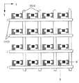
図1は、本発明の画像形成装置が備える表示パネルの斜視図であり、内部構造を示すためにパネルの一部を切り欠いて示している。
【0037】
図中、1015はリアプレート、1016は側壁、1017はフェースプレートであり、1015〜1017により表示パネルの内部を真空に維持するための気密容器を形成している。気密容器を組み立てるにあたっては、各部材の接合部に十分な強度と気密性を保持させるため封着する必要があるが、たとえばフリットガラスを接合部に塗布し、大気中あるいは窒素雰囲気中で、摂氏400〜500度で10分以上焼成することにより封着を達成した。気密容器内部を真空に排気する方法については後述する。また、上記気密容器の内部は10のマイナス6乗[Torr]程度の真空に保持されるので、大気圧や不意の衝撃などによる気密容器の破壊を防止する目的で、耐大気圧構造体として、スペーサ1020が設けられている。
【0038】
次に、本発明の画像形成装置に用いることができる電子放出素子基板について説明する。本発明の画像形成装置に用いられる電子源基板は複数の冷陰極素子を基板上に配列することにより形成される。
【0039】
冷陰極素子の配列の方式には、冷陰極素子を並列に配置し、個々の素子の両端を配線で接続するはしご型配置(以下、はしご型配置電子源基板と称する)や、冷陰極素子の一対の素子電極のそれぞれX方向配線、Y方向配線を接続した単純マトリクス配置(以下、マトリクス型配置電子源基板と称する)が挙げられる。なお、はしご型配置電子源基板を有する画像形成装置には、電子放出素子からの電子の飛翔を制御する電極である制御電極(グリッド電極)を必要とする。
【0040】
リアプレート1015には、基板1011が固定されているが、該基板上には冷陰極素子1012がn×m個形成されている。(n,mは2以上の正の整数であり、目的とする表示画素数に応じて適宜設定される。たとえば、高品位テレビジョンの表示を目的とした表示装置においては、n=3000,m=1000以上の数を設定することが望ましい。)前記n×m個の冷陰極素子は、m本の行方向配線1013とn本の列方向配線1014により単純マトリクス配線されている。前記、1011〜1014によって構成される部分をマルチ電子ビーム源と呼ぶ。
【0041】
本発明の画像表示装置に用いるマルチ電子ビーム源は、冷陰極素子を単純マトリクス配線もしくは、はしご型配置した電子源であれば、冷陰極素子の材料や形状あるいは製法に制限はない。
【0042】
したがって、たとえば表面伝導型電子放出素子やFE型、あるいはMIM型などの冷陰極素子を用いることができる。
【0043】
次に、冷陰極素子として表面伝導型電子放出素子を基板上に配列して単純マトリクス配線したマルチ電子ビーム源の構造について述べる。
【0044】
図2に示すのは、図1の表示パネルに用いたマルチ電子ビーム源の平面図である。基板1011上には、表面伝導型電子放出素子が配列され、これらの素子は行方向配線1013と列方向配線1014により単純マトリクス状に配線されている。行方向配線1013と列方向配線1014の交差する部分には、電極間に絶縁層(不図示)が形成されており、電気的な絶縁が保たれている。
【0045】
図2のB−B′に沿った断面を、図3に示す。
【0046】
なお、このような構造のマルチ電子源は、あらかじめ基板上に行方向配線1013、列方向配線1014、電極間絶縁層(不図示)、および表面伝導型電子放出素子の素子電極と導電性薄膜を形成した後、行方向配線1013および列方向配線1014を介して各素子に給電して通電フォーミング処理(後述)と通電活性化処理(後述)を行うことにより製造した。
【0047】
本実施形態においては、気密容器のリアプレート1015にマルチ電子ビーム源の基板1011を固定する構成としたが、マルチ電子ビーム源の基板1011が十分な強度を有するものである場合には、気密容器のリアプレートとしてマルチ電子ビーム源の基板1011自体を用いてもよい。
【0048】
また、フェースプレート1017の下面には、蛍光膜1018が形成されている。本実施例はカラー表示装置であるため、蛍光膜1018の部分にはCRTの分野で用いられる赤、緑、青、の3原色の蛍光体が塗り分けられている。各色の蛍光体は、たとえば図4(a)に示すようにストライプ状に塗り分けられ、蛍光体のストライプの間には黒色の導電体1010が設けてある。黒色の導電体1010を設ける目的は、電子ビームの照射位置に多少のずれがあっても表示色にずれが生じないようにする事や、外光の反射を防止して表示コストラストの低下を防ぐ事、電子ビームによる蛍光膜のチャージアップを防止する事などである。黒色の導電体1010には、黒鉛を主成分として用いたが、上記の目的に適するものであればこれ以外の材料を用いても良い。
【0049】
また、3原色の蛍光体の塗り分け方は前記図4(a)に示したストライプ状の配列に限られるものではなく、たとえば図4(b)に示すようなデルタ状配列や、それ以外の配列であってもよい。
【0050】
なお、モノクロームの表示パネルを作成する場合には、単色の蛍光体材料を蛍光膜1018に用いればよく、また黒色導電材料は必ずしも用いなくともよい。
【0051】
また、蛍光膜1018のリアプレート側の面には、CRTの分野では公知のメタルバック1019を設けてある。メタルバック1019を設けた目的は、蛍光膜1018が発する光の一部を鏡面反射して光利用率を向上させる事や、負イオンの衝突から蛍光膜1018を保護する事や、電子ビーム加速電圧を印加するための電極として作用させる事や、蛍光膜1018を励起した電子の導電路として作用させる事などである。メタルバック1019は、蛍光膜1018をフェースプレート基板1017上に形成した後、蛍光膜表面を平滑化処理し、その上にAlを真空蒸着する方法により形成した。なお、蛍光膜1018に低電圧用の蛍光体材料を用いた場合には、メタルバック1019は用いない。
【0052】
また、加速電圧の印加用や蛍光膜の導電性向上を目的として、フェースプレート基板1017と蛍光膜1018との間に、たとえばITOを材料とする透明電極を設けてもよい。
【0053】
画像表示領域内に配置されるスペーサについて説明する。図5は図1のA−A′のスペーサ1020を拡大した部位の断面模式図であり、各部の番号は図1に対応している。スペーサ1020Aは絶縁性部材1の表面に帯電防止を目的とした高抵抗膜11を成膜し、かつフェースプレート1017の内側(メタルバック1019等)及び基板1011の表面(行方向配線1013または列方向配線1014)に面したスペーサの当接面3及び接する側面部5に低抵抗膜21を成膜した部材からなるもので、上記目的を達成するのに必要な数だけ、かつ必要な間隔をおいて配置され、フェースプレートの内側および基板1011の表面に接合材1041により固定される。また、高抵抗膜は、絶縁性部材1の表面のうち、少なくとも気密容器内の真空中に露出している面に成膜されており、スペーサ1020A上の低抵抗膜21および接合材1041を介して、フェースプレート1017の内側(メタルバック1019等)及び基板1011の表面(行方向配線1013または列方向配線1014)に電気的に接続される。ここで説明される態様においては、スペーサ1020の形状は薄板状とし、行方向配線1013に平行に配置され、行方向配線1013に電気的に接続されている。
【0054】
スペーサ1020としては、基板1011上の行方向配線1013および列方向配線1014とフェースプレート1017内面のメタルバック1019との間に印加される高電圧に耐えるだけの絶縁性を有し、かつスペーサ1020の表面への帯電を防止する程度の導電性を有する必要がある。
【0055】
スペーサ1020の絶縁性部材1としては、例えば石英ガラス、Na等の不純物含有量を減少したガラス、ソーダライムガラス、アルミナ等のセラミックス部材等が挙げられる。なお、絶縁性部材1はその熱膨張率が気密容器および基板1011を成す部材と近いものが好ましい。
【0056】
スペーサ1020を構成する高抵抗膜11には、高電位側のフェースプレート1017(メタルバック1019等)に印加される加速電圧Vaを帯電防止膜である高抵抗膜21の抵抗値Rsで除した電流が流される。そこで、スペーサの抵抗値Rsは帯電防止および消費電力からその望ましい範囲に設定される。帯電防止の観点から表面抵抗R/□は10の12乗Ω以下であることが好ましい。十分な帯電防止効果を得るためには10の11乗Ω以下がさらに好ましい。表面抵抗の下限はスペーサ形状とスペーサ間に印加される電圧により左右されるが、10の5乗Ω以上であることが好ましい。
【0057】
絶縁材料上に形成された帯電防止膜の厚みtは10nm〜1μmの範囲が望ましい。材料の表面エネルギーおよび基板との密着性や基板温度によっても異なるが、一般的に10nm以下の薄膜は島状に形成され、抵抗が不安定で再現性に乏しい。一方、膜厚tが1μm以上では膜応力が大きくなって膜はがれの危険性が高まり、かつ成膜時間が長くなるため生産性が悪い。従って、膜厚は50〜500nmであることが望ましい。表面抵抗R/□はρ/tであり、以上に述べたR□とtの好まし範囲から、帯電防止膜の比抵抗ρは0.1[Ωcm]乃至10の8乗[Ωcm]が好ましい。さらに表面抵抗と膜厚のより好まし範囲を実現するためには、ρは10の2乗乃至10の6乗Ωcmとするのが良い。
【0058】
スペーサは上述したようにその上に形成した帯電防止膜を電流が流れることにより、あるいはディスプレイ全体が動作中に発熱することによりその温度が上昇する。帯電防止膜の抵抗温度係数が大きな負の値であると温度が上昇した時に抵抗値が減少し、スペーサに流れる電流が増加し、さらに温度上昇をもたらす。そして電流は電源の限界を越えるまで増加しつづける。このような電流の暴走が発生する抵抗温度係数の値は経験的に負の値で絶対値が1%以上である。すなわち、帯電防止膜の抵抗温度係数は−1%未満であることが望ましい。
【0059】
帯電防止特性を有する高抵抗膜11の材料としては、例えば金属酸化物を用いることが出来る。金属酸化物の中でも、クロム、ニッケル、銅の酸化物が好ましい材料である。その理由はこれらの酸化物は二次電子放出効率が比較的小さく、冷陰極素子1012から放出された電子がスペーサ1020に当たった場合においても帯電しにくいためと考えられる。金属酸化物以外にも炭素は二次電子放出効率が小さく好ましい材料である。特に、非晶質カーボンは高抵抗であるため、スペーサ抵抗を所望の値に制御しやすい。
【0060】
帯電防止特性を有する高抵抗膜11の他の材料として、アルミと遷移金属合金の窒化物は遷移金属の組成を調整することにより、良伝導体から絶縁体まで広い範囲に抵抗値を制御できるので好適な材料である。さらには後述する表示装置の作製工程において抵抗値の変化が少なく安定な材料である。かつ、その抵抗温度係数が−1%未満であり、実用的に使いやすい材料である。遷移金属元素としてはTi,Cr,Ta等があげられる。
【0061】
合金窒化膜はスパッタ、窒素ガス雰囲気中での反応性スパッタ、電子ビーム蒸着、イオンプレーティング、イオンアシスト蒸着法等の薄膜形成手段により絶縁性部材上に形成される。金属酸化膜も同様の薄膜形成法で作製することができるが、この場合窒素ガスに代えて酸素ガスを使用する。その他、CVD法、アルコキシド塗布法でも金属酸化膜を形成できる。カーボン膜は蒸着法、スパッタ法、CVD法、プラズマCVD法で作製され、特に非晶質カーボンを作製する場合には、成膜中の雰囲気に水素が含まれるようにするか、成膜ガスに炭化水素ガスを使用する。
【0062】
スペーサ1020Aを構成する低抵抗膜21は、高抵抗膜11を高電位側のフェースプレート1017(メタルバック1019等)及び低電位側の基板1011(配線1013、1014等)と電気的に接続する為に設けられたものであり、以下では、中間電極層(中間層)という名称も用いる。中間電極層(中間層)は以下に列挙する複数の機能を有することが出来る。
【0063】
高抵抗膜11をフェースプレート1017及び基板1011と電気的に接続する。
【0064】
既に記載したように、高抵抗膜11はスペーサ1020表面での帯電を防止する目的で設けられたものであるが、高抵抗膜11をフェースプレート1017(メタルバック1019等)及び基板1011(配線1013、1014等)と直接或いは当接材1041を介して接続した場合、接続部界面に大きな接触抵抗が発生し、スペーサ表面に発生した電荷を速やかに除去できなくなる可能性がある。これを避ける為に、フェースプレート1017、基板1011及び当接材1041と接触するスペーサ1020の当接面3或いは側面部5に低抵抗の中間層を設けた。
【0065】
冷陰極素子1012より放出された電子は、フェースプレート1017と基板1011の間に形成された電位分布に従って電子軌道を成す。スペーサ1020の近傍で電子軌道に乱れが生じないようにする為には、高抵抗膜11の電位分布を全域にわたって制御する必要がある。高抵抗膜11をフェースプレート1017(メタルバック1019等)及び基板1011(配線1013、1014等)と直接或いは当接材1041を介して接続した場合、接続部界面の接触抵抗の為に、接続状態のむらが発生し、高抵抗膜11の電位分布が所望の値からずれてしまう可能性がある。これを避ける為に、スペーサ1020がフェースプレート1017及び基板1011と当接するスペーサ端部(当接面3或いは側面部5)の全長域に低抵抗の中間層を設け、この中間層部に所望の電位を印加することによって、高抵抗膜11全体の電位を制御可能とした。
【0066】
冷陰極素子1012より放出された電子は、フェースプレート1017と基板1011の間に形成された電位分布に従って電子軌道を成す。スペーサ近傍の冷陰極素子から放出された電子に関しては、スペーサを設置することに伴う制約(配線、素子位置の変更等)が生じる場合がある。このような場合、歪みやむらの無い画像を形成する為には、放出された電子の軌道を制御してフェースプレート1017上の所望の位置に電子を照射する必要がある。フェースプレート1017及び基板1011と当接する面の側面部5に低抵抗の中間層を設けることにより、スペーサ1020近傍の電位分布に所望の特性を持たせ、放出された電子の軌道を制御することが出来る。
【0067】
低抵抗膜21は、高抵抗膜11に比べ十分に低い抵抗値を有する材料を選択すればよく、Ni,Cr,Au,Mo,W,Pt,Ti,Al,Cu,Pd等の金属、あるいは合金、及びPd,Ag,Au,RuO 2,Pd−Ag等の金属や金属酸化物とガラス等から構成される印刷導体、あるいはIn 2 O 3−SnO 2等の透明導体及びポリシリコン等の半導体材料等より適宜選択される。
【0068】
接合材1041はスペーサ1020が行方向配線1013およびメタルバック1019と電気的に接続するように、導電性をもたせる必要がある。すなわち、導電性接着材や金属粒子や導電性フィラーを添加したフリットガラスが好適である。
【0069】
また、Dx1〜DxmおよびDy1〜DynおよびHvは、当該表示パネルと不図示の電気回路とを電気的に接続するために設けた気密構造の電気接続用端子である。Dx1〜Dxmはマルチ電子ビーム源の行方向配線1013と、Dy1〜Dynはマルチ電子ビーム源の列方向配線1014と、Hvはフェースプレートのメタルバック1019と電気的に接続している。
【0070】
また、気密容器内部を真空に排気するには、気密容器を組み立てた後、不図示の排気管と真空ポンプとを接続し、気密容器内を10のマイナス7乗[Torr]程度の真空度まで排気する。その後、排気管を封止するが、気密容器内の真空度を維持するために、封止の直前あるいは封止後に気密容器内の所定の位置にゲッター膜(不図示)を形成する。ゲッター膜とは、たとえばBaを主成分とするゲッター材料をヒーターもしくは高周波加熱により加熱し蒸着して形成した膜であり、該ゲッター膜の吸着作用により気密容器内は1×10マイナス5乗ないしは1×10マイナス7乗[Torr]の真空度に維持される。
【0071】
以上説明した表示パネルを用いた画像表示装置は、容器外端子Dx1ないしDxm、Dy1ないしDynを通じて各冷陰極素子1012に電圧を印加すると、各冷陰極素子1012から電子が放出される。それと同時にメタルバック1019に容器外端子Hvを通じて数百[V]ないし数[kV]の高圧を印加して、上記放出された電子を加速し、フェースプレート1017の内面に衝突させる。これにより、蛍光膜1018をなす各色の蛍光体が励起されて発光し、画像が表示される。
【0072】
通常、冷陰極素子である本発明の表面伝導型電子放出素子への1012への印加電圧は12〜16[V]程度、メタルバック1019と冷陰極素子1012との距離dは0.1[mm]から8[mm]程度、メタルバック1019と冷陰極素子1012間の電圧0.1[kV]から10[kV]程度である。
【0073】
以上、本発明の表示パネルの基本構成と製法、および画像表示装置の概要を説明した。
【0074】
次に、前記表示パネルに用いたマルチ電子ビーム源の製造方法について説明する。本発明の画像表示装置に用いるマルチ電子ビーム源は、冷陰極素子を単純マトリクス配線した電子源であれば、冷陰極素子の材料や形状あるいは製法に制限はない。したがって、たとえば表面伝導型電子放出素子やFE型、あるいはMIM型などの冷陰極素子を用いることができる。
【0075】
ただし、表示画面が大きくてしかも安価な表示装置が求められる状況のもとでは、これらの冷陰極素子の中でも、表面伝導型電子放出素子が特に好ましい。すなわち、FE型ではエミッタコーンとゲート電極の相対位置や形状が電子放出特性を大きく左右するため、極めて高精度の製造技術を必要とするが、これは大面積化や製造コストの低減を達成するには不利な要因となる。また、MIM型では、絶縁層と上電極の膜厚を薄くてしかも均一にする必要があるが、これも大面積化や製造コストの低減を達成するには不利な要因となる。その点、表面伝導型電子放出素子は、比較的製造方法が単純なため、大面積化や製造コストの低減が容易である。また、発明者らは、表面伝導型電子放出素子の中でも、電子放出部もしくはその周辺部を微粒子膜から形成したものがとりわけ電子放出特性に優れ、しかも製造が容易に行えることを見いだしている。したがって、高輝度で大画面の画像表示装置のマルチ電子ビーム源に用いるには、最も好適であると言える。そこで、上記実施例の表示パネルにおいては、電子放出部もしくはその周辺部を微粒子膜から形成した表面伝導型電子放出素子を用いた。そこで、まず好適な表面伝導型電子放出素子について基本的な構成と製法および特性を説明し、その後で多数の素子を単純マトリクス配線したマルチ電子ビーム源の構造について述べる。
【0076】
(表面伝導型電子放出素子の好適な素子構成と製法)
電子放出部もしくはその周辺部を微粒子膜から形成する表面伝導型電子放出素子の代表的な構成には、平面型と垂直型の2種類があげられる。
【0077】
(平面型の表面伝導型電子放出素子)
まず最初に、平面型の表面伝導型電子放出素子の素子構成と製法について説明する。
【0078】
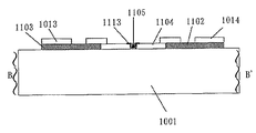
図6に示すのは、平面型の表面伝導型電子放出素子の構成を説明するための平面図(a)および断面図(b)である。図中、1101は基板、1102と1103は素子電極、1104は導電性薄膜、1105は通電フォーミング処理により形成した電子放出部、1113は通電活性化処理により形成した薄膜である。
【0079】
基板1101としては、たとえば、石英ガラスや青板ガラスをはじめとする各種ガラス基板や、アルミナをはじめとする各種セラミクス基板、あるいは上述の各種基板上にたとえばSiO 2 を材料とする絶縁層を積層した基板、などを用いることができる。
【0080】
また、基板1101上に基板面と平行に対向して設けられた素子電極1102と1103は、導電性を有する材料によって形成されている。たとえば、Ni,Cr,Au,Mo,W,Pt,Ti,Cu,Pd,Ag等をはじめとする金属、あるいはこれらの金属の合金、あるいはIn 2 O 3 −SnO 2 をはじめとする金属酸化物、ポリシリコンなどの半導体、などの中から適宜材料を選択して用いればよい。電極を形成するには、たとえば真空蒸着などの製膜技術とフォトリソグラフィー、エッチングなどのパターニング技術を組み合わせて用いれば容易に形成できるが、それ以外の方法(たとえば印刷技術)を用いて形成してもさしつかえない。
【0081】
素子電極1102と1103の形状は、当該電子放出素子の応用目的に合わせて適宜設計される。一般的には、電極間隔Lは通常は数百オングストロームから数百マイクロメーターの範囲から適当な数値を選んで設計されるが、なかでも表示装置に応用するために好ましいのは数マイクロメーターより数十マイクロメーターの範囲である。また、素子電極の厚さdについては、通常は数百オングストロームから数マイクロメーターの範囲から適当な数値が選ばれる。
【0082】
また、導電性薄膜1104の部分には、微粒子膜を用いる。ここで述べた微粒子膜とは、構成要素として多数の微粒子を含んだ膜(島状の集合体も含む)のことをさす。微粒子膜を微視的に調べれば、通常は、個々の微粒子が離間して配置された構造か、あるいは微粒子が互いに隣接した構造か、あるいは微粒子が互いに重なり合った構造が観測される。
【0083】
微粒子膜に用いた微粒子の粒径は、数オングストロームから数千オングストロームの範囲に含まれるものであるが、なかでも好ましいのは10オングストロームから200オングストロームの範囲のものである。また、微粒子膜の膜厚は、以下に述べるような諸条件を考慮して適宜設定される。すなわち、素子電極1102あるいは1103と電気的に良好に接続するのに必要な条件、後述する通電フォーミングを良好に行うのに必要な条件、微粒子膜自身の電気抵抗を後述する適宜の値にするために必要な条件、などである。具体的には、数オングストロームから数千オングストロームの範囲のなかで設定するが、なかでも好ましいのは10オングストロームから500オングストロームの間である。
【0084】
また、微粒子膜を形成するのに用いられうる材料としては、たとえば、Pd,Pt,Ru,Ag,Au,Ti,In,Cu,Cr,Fe,Zn,Sn,Ta,W,Pb,などをはじめとする金属や、PdO,SnO 2 ,In 2 O 3,PbO,Sb 2 O 3 ,などをはじめとする酸化物や、HfB 2,ZrB 2 ,LaB 6 ,CeB 6 ,YB 4 ,GdB 4 ,などをはじめとする硼化物や、TiC,ZrC,HfC,TaC,SiC,WC,などをはじめとする炭化物や、TiN,ZrN,HfN,などをはじめとする窒化物や、Si,Ge,などをはじめとする半導体や、カーボン、などがあげられ、これらの中から適宜選択される。
【0085】
以上述べたように、導電性薄膜1104を微粒子膜で形成したが、そのシート抵抗値については、10の3乗から10の7乗[オーム/sq]の範囲に含まれるよう設定した。
【0086】
なお、導電性薄膜1104と素子電極1102および1103とは、電気的に良好に接続されるのが望ましいため、互いの一部が重なりあうような構造をとっている。その重なり方は、図6の例においては、下から、基板、素子電極、導電性薄膜の順序で積層したが、場合によっては下から基板、導電性薄膜、素子電極、の順序で積層してもさしつかえない。
【0087】
また、電子放出部1105は、導電性薄膜1104の一部に形成された亀裂状の部分であり、電気的には周囲の導電性薄膜よりも高抵抗な性質を有している。亀裂は、導電性薄膜1104に対して、後述する通電フォーミングの処理を行うことにより形成する。亀裂内には、数オングストロームから数百オングストロームの粒径の微粒子を配置する場合がある。なお、実際の電子放出部の位置や形状を精密かつ正確に図示するのは困難なため、図6においては模式的に示した。
【0088】
また、薄膜1113は、炭素もしくは炭素化合物よりなる薄膜で、電子放出部1105およびその近傍を被覆している。薄膜1113は、通電フォーミング処理後に、後述する通電活性化の処理を行うことにより形成する。
【0089】
薄膜1113は、単結晶グラファイト、多結晶グラファイト、非晶質カーボン、のいずれかか、もしくはその混合物であり、膜厚は500[オングストローム]以下とするが、300[オングストローム]以下とするのがさらに好ましい。なお、実際の薄膜1113の位置や形状を精密に図示するのは困難なため、図112においては模式的に示した。また、平面図(a)においては、薄膜1113の一部を除去した素子を図示した。
【0090】
以上、好ましい素子の基本構成を述べたが、実施例においては以下のような素子を用いた。
【0091】
すなわち、基板1101には青板ガラスを用い、素子電極1102と1103にはNi薄膜を用いた。素子電極の厚さdは1000[オングストローム]、電極間隔Lは2[マイクロメーター]とした。
【0092】
微粒子膜の主要材料としてPdもしくはPdOを用い、微粒子膜の厚さは約100[オングストローム]、幅Wは100[マイクロメータ]とした。
【0093】
次に、好適な平面型の表面伝導型電子放出素子の製造方法について説明する。
【0094】
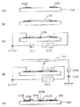
図7(a)〜(d)は、表面伝導型電子放出素子の製造工程を説明するための断面図で、各部材の表記は前記図6と同一である。
【0095】
1)まず、図7(a)に示すように、基板1101上に素子電極1102および1103を形成する。
【0096】
形成するにあたっては、あらかじめ基板1101を洗剤、純水、有機溶剤を用いて十分に洗浄後、素子電極の材料を堆積させる。(堆積する方法としては、たとえば、蒸着法やスパッタ法などの真空成膜技術を用ればよい。)その後、堆積した電極材料を、フォトリソグラフィー・エッチング技術を用いてパターニングし、(a)に示した一対の素子電極(1102と1103)を形成する。
【0097】
2)次に、同図(b)に示すように、導電性薄膜1104を形成する。
【0098】
形成するにあたっては、まず前記(a)の基板に有機金属溶液を塗布して乾燥し、加熱焼成処理して微粒子膜を成膜した後、フォトリソグラフィー・エッチングにより所定の形状にパターニングする。ここで、有機金属溶液とは、導電性薄膜に用いる微粒子の材料を主要元素とする有機金属化合物の溶液である。(具体的には、本実施例では主要元素としてPdを用いた。また、実施例では塗布方法として、ディッピング法を用いたが、それ以外のたとえばスピンナー法やスプレー法を用いてもよい。)
また、微粒子膜で作られる導電性薄膜の成膜方法としては、本実施例で用いた有機金属溶液の塗布による方法以外の、たとえば真空蒸着法やスパッタ法、あるいは化学的気相堆積法などを用いる場合もある。
【0099】
3)次に、同図(c)に示すように、フォーミング用電源1110から素子電極1102と1103の間に適宜の電圧を印加し、通電フォーミング処理を行って、電子放出部1105を形成する。
【0100】
通電フォーミング処理とは、微粒子膜で作られた導電性薄膜1104に通電を行って、その一部を適宜に破壊、変形、もしくは変質せしめ、電子放出を行うのに好適な構造に変化させる処理のことである。微粒子膜で作られた導電性薄膜のうち電子放出を行うのに好適な構造に変化した部分(すなわち電子放出部1105)においては、薄膜に適当な亀裂が形成されている。なお、電子放出部1105が形成される前と比較すると、形成された後は素子電極1102と1103の間で計測される電気抵抗は大幅に増加する。
【0101】
通電方法をより詳しく説明するために、図8において、フォーミング用電源1110から印加する適宜の電圧波形の一例を示す。微粒子膜で作られた導電性薄膜をフォーミングする場合には、パルス状の電圧が好ましく、本実施例の場合には同図に示したようにパルス幅T1の三角波パルスをパルス間隔T2で連続的に印加した。その際には、三角波パルスの波高値Vpfを、順次昇圧した。また、電子放出部1105の形成状況をモニターするためのモニターパルスPmを適宜の間隔で三角波パルスの間に挿入し、その際に流れる電流を電流計1111で計測した。
【0102】
実施例においては、たとえば10のマイナス5乗[torr]程度の真空雰囲気下において、たとえばパルス幅T1を1[ミリ秒]、パルス間隔T2を10[ミリ秒]とし、波高値Vpfを1パルスごとに0.1[V]ずつ昇圧した。そして、三角波を5パルス印加するたびに1回の割りで、モニターパルスPmを挿入した。フォーミング処理に悪影響を及ぼすことがないように、モニターパルスの電圧Vpmは0.1[V]に設定した。そして、素子電極1102と1103の間の電気抵抗が1×10の6乗[オーム]になった段階、すなわちモニターパルス印加時に電流計1111で計測される電流が1×10のマイナス7乗[A]以下になった段階で、フォーミング処理にかかわる通電を終了した。
【0103】
なお、上記の方法は、本実施例の表面伝導型電子放出素子に関する好ましい方法であり、たとえば微粒子膜の材料や膜厚、あるいは素子電極間隔Lなど表面伝導型電子放出素子の設計を変更した場合には、それに応じて通電の条件を適宜変更するのが望ましい。
【0104】
4)次に、図7(d)に示すように、活性化用電源1112から素子電極1102と1103の間に適宜の電圧を印加し、通電活性化処理を行って、電子放出特性の改善を行う。
【0105】
通電活性化処理とは、前記通電フォーミング処理により形成された電子放出部1105に適宜の条件で通電を行って、その近傍に炭素もしくは炭素化合物を堆積せしめる処理のことである。(図においては、炭素もしくは炭素化合物よりなる堆積物を部材1113として模式的に示した。)なお、通電活性化処理を行うことにより、行う前と比較して、同じ印加電圧における放出電流を典型的には100倍以上に増加させることができる。
【0106】
具体的には、10のマイナス4乗ないし10のマイナス5乗[torr]の範囲内の真空雰囲気中で、電圧パルスを定期的に印加することにより、真空雰囲気中に存在する有機化合物を起源とする炭素もしくは炭素化合物を堆積させる。堆積物1113は、単結晶グラファイト、多結晶グラファイト、非晶質カーボン、のいずれかか、もしくはその混合物であり、膜厚は500[オングストローム]以下、より好ましくは300[オングストローム]以下である。
【0107】
通電方法をより詳しく説明するために、図9(a)に、活性化用電源1112から印加する適宜の電圧波形の一例を示す。本実施例においては、一定電圧の矩形波を定期的に印加して通電活性化処理を行ったが、具体的には、矩形波の電圧Vacは14[V],パルス幅T3は1[ミリ秒],パルス間隔T4は10[ミリ秒]とした。なお、上述の通電条件は、本実施例の表面伝導型電子放出素子に関する好ましい条件であり、表面伝導型電子放出素子の設計を変更した場合には、それに応じて条件を適宜変更するのが望ましい。
【0108】
図7(d)に示す1114は該表面伝導型電子放出素子から放出される放出電流Ieを捕捉するためのアノード電極で、直流高電圧電源1115および電流計1116が接続されている。(なお、基板1101を、表示パネルの中に組み込んでから活性化処理を行う場合には、表示パネルの蛍光面をアノード電極1114として用いる。)活性化用電源1112から電圧を印加する間、電流計1116で放出電流Ieを計測して通電活性化処理の進行状況をモニターし、活性化用電源1112の動作を制御する。
【0109】
図9(b)には、電流計1116で計測された放出電流Ieの一例を示す。活性化電源1112からパルス電圧を印加しはじめると、時間の経過とともに放出電流Ieは増加するが、やがて飽和してほとんど増加しなくなる。このように、放出電流Ieがほぼ飽和した時点で活性化用電源1112からの電圧印加を停止し、通電活性化処理を終了する。
【0110】
なお、上述の通電条件は、本実施例の表面伝導型電子放出素子に関する好ましい条件であり、表面伝導型電子放出素子の設計を変更した場合には、それに応じて条件を適宜変更するのが望ましい。
【0111】
以上のようにして、図7(e)に示す平面型の表面伝導型電子放出素子を製造した。
【0112】
(垂直型の表面伝導型電子放出素子)
次に、電子放出部もしくはその周辺を微粒子膜から形成した表面伝導型電子放出素子のもうひとつの代表的な構成、すなわち垂直型の表面伝導型電子放出素子の構成について説明する。
【0113】
図10は、垂直型の基本構成を説明するための模式的な断面図であり、図中の1201は基板、1202と1203は素子電極、1206は段差形成部材、1204は微粒子膜を用いた導電性薄膜、1205は通電フォーミング処理により形成した電子放出部、1213は通電活性化処理により形成した薄膜、である。
【0114】
垂直型が先に説明した平面型と異なる点は、素子電極のうちの片方(1202)が段差形成部材1206上に設けられており、導電性薄膜1204が段差形成部材1206の側面を被覆している点にある。したがって、前記図6の平面型における素子電極間隔Lは、垂直型においては段差形成部材1206の段差高Lsとして設定される。なお、基板1201、素子電極1202および1203、微粒子膜を用いた導電性薄膜1204、については、前記平面型の説明中に列挙した材料を同様に用いることが可能である。また、段差形成部材1206には、たとえばSiO 2のような電気的に絶縁性の材料を用いる。
【0115】
次に、垂直型の表面伝導型電子放出素子の製法について説明する。図11(a)〜(f)は、製造工程を説明するための断面図で、各部材の表記は前記図10と同一である。
【0116】
1)まず、図11(a)に示すように、基板1201上に素子電極1203を形成する。
【0117】
2)次に、同図(b)に示すように、段差形成部材を形成するための絶縁層を積層する。絶縁層は、たとえばSiO 2 をスパッタ法で積層すればよいが、たとえば真空蒸着法や印刷法などの他の成膜方法を用いてもよい。
【0118】
3)次に、同図(c)に示すように、絶縁層の上に素子電極1202を形成する。
【0119】
4)次に、同図(d)に示すように、絶縁層の一部を、たとえばエッチング法を用いて除去し、素子電極1203を露出させる。
【0120】
5)次に、同図(e)に示すように、微粒子膜を用いた導電性薄膜1204を形成する。形成するには、前記平面型の場合と同じく、たとえば塗布法などの成膜技術を用いればよい。
【0121】
6)次に、前記平面型の場合と同じく、通電フォーミング処理を行い、電子放出部を形成する。(図7(c)を用いて説明した平面型の通電フォーミング処理と同様の処理を行えばよい。)
7)次に、前記平面型の場合と同じく、通電活性化処理を行い、電子放出部近傍に炭素もしくは炭素化合物を堆積させる。(図7(d)を用いて説明した平面型の通電活性化処理と同様の処理を行えばよい。)
以上のようにして、図11(f)に示す垂直型の表面伝導型電子放出素子を製造した。
【0122】
(表示装置に用いた表面伝導型電子放出素子の特性)
以上、平面型と垂直型の表面伝導型電子放出素子について素子構成と製法を説明したが、次に表示装置に用いた素子の特性について述べる。
【0123】
図12に、表示装置に用いた素子の、(放出電流Ie)対(素子印加電圧Vf)特性、および(素子電流If)対(素子印加電圧Vf)特性の典型的な例を示す。なお、放出電流Ieは素子電流Ifに比べて著しく小さく、同一尺度で図示するのが困難であるうえ、これらの特性は素子の大きさや形状等の設計パラメータを変更することにより変化するものであるため、2本のグラフは各々任意単位で図示した。
【0124】
表示装置に用いた素子は、放出電流Ieに関して以下に述べる3つの特性を有している。
【0125】
第一に、ある電圧(これを閾値電圧Vthと呼ぶ)以上の大きさの電圧を素子に印加すると急激に放出電流Ieが増加するが、一方、閾値電圧Vth未満の電圧では放出電流Ieはほとんど検出されない。
【0126】
すなわち、放出電流Ieに関して、明確な閾値電圧Vthを持った非線形素子である。
【0127】
第二に、放出電流Ieは素子に印加する電圧Vfに依存して変化するため、電圧Vfで放出電流Ieの大きさを制御できる。
【0128】
第三に、素子に印加する電圧Vfに対して素子から放出される電流Ieの応答速度が速いため、電圧Vfを印加する時間の長さによって素子から放出される電子の電荷量を制御できる。
【0129】
以上のような特性を有するため、表面伝導型電子放出素子を表示装置に好適に用いることができた。たとえば多数の素子を表示画面の画素に対応して設けた表示装置において、第一の特性を利用すれば、表示画面を順次走査して表示を行うことが可能である。すなわち、駆動中の素子には所望の発光輝度に応じて閾値電圧Vth以上の電圧を適宜印加し、非選択状態の素子には閾値電圧Vth未満の電圧を印加する。駆動する素子を順次切り替えてゆくことにより、表示画面を順次走査して表示を行うことが可能である。
【0130】
また、第二の特性かまたは第三の特性を利用することにより、発光輝度を制御することができるため、階調表示を行うことが可能である。
【0131】
(多数素子を単純マトリクス配線したマルチ電子ビーム源の構造)
次に、上述の表面伝導型電子放出素子を基板上に配列して単純マトリクス配線したマルチ電子ビーム源の構造について述べる。
【0132】
図2に示すのは、前記図1の表示パネルに用いたマルチ電子ビーム源の平面図である。基板上には、前記図1で示したものと同様な表面伝導型電子放出素子が配列され、これらの素子は行方向配線電極1013と列方向配線電極1014により単純マトリクス状に配線されている。行方向配線電極1013と列方向配線電極1014の交差する部分には、電極間に絶縁層(不図示)が形成されており、電気的な絶縁が保たれている。
【0133】
図2のB−B′に沿った断面を、図3に示す。
【0134】
なお、このような構造のマルチ電子源は、あらかじめ基板上に行方向配線電極1013、列方向配線電極1014、電極間絶縁層(不図示)、および表面伝導型電子放出素子の素子電極と導電性薄膜を形成した後、行方向配線電極1013および列方向配線電極1014を介して各素子に給電して通電フォーミング処理と通電活性化処理を行うことにより製造した。
【0135】
(駆動回路構成および駆動方法)
図13は、NTSC方式のテレビ信号に基づいてテレビジョン表示を行う為の駆動回路の概略構成をブロック図で示したものである。同図中、表示パネル1701は前述した表示パネルに相当するもので、前述した様に製造され、動作する。また、走査回路1702は表示ラインを走査し、制御回路1703は走査回路へ入力する信号等を生成する。シフトレジスタ1704は1ライン毎のデータをシフトし、ラインメモリ1705は、シフトレジスタ1704からの1ライン分のデータを変調信号発生器1707に入力する。同期信号分離回路1706はNTSC信号から同期信号を分離する。
【0136】
以下、図13の装置各部の機能を詳しく説明する。
【0137】
まず表示パネル1701は、端子Dx1ないしDxmおよび端子Dy1ないしDyn、および高圧端子Hvを介して外部の電気回路と接続されている。このうち、端子Dx1ないしDxmには、表示パネル1701内に設けられているマルチ電子ビーム源、すなわちm行n列の行列状にマトリクス配線された冷陰極素子を1行(n素子)ずつ順次駆動してゆく為の走査信号が印加される。一方、端子Dy1ないしDynには、前記走査信号により選択された1行分のn個の各素子の出力電子ビームを制御する為の変調信号が印加される。また、高圧端子Hvには、直流電圧源Vaより、たとえば5[kV]の直流電圧が供給されるが、これはマルチ電子ビーム源より出力される電子ビームに蛍光体を励起するのに十分なエネルギーを付与する為の加速電圧である。
【0138】
次に、走査回路1702について説明する。同回路は、内部にm個のスイッチング素子(図中、S1ないしSmで模式的に示されている)を備えるもので、各スイッチング素子は、直流電圧源Vxの出力電圧もしくは0[V](グランドレベル)のいずれか一方を選択し、表示パネル1701の端子Dx1ないしDxmと電気的に接続するものである。S1ないしSmの各スイッチング素子は、制御回路1703が出力する制御信号Tscanに基づいて動作するものだが、実際にはたとえばFETのようなスイッチング素子を組合わせる事により容易に構成することが可能である。なお、前記直流電圧源Vxは、図118に例示した電子放出素子の特性に基づき走査されていない素子に印加される駆動電圧が電子放出しきい値電圧Vth電圧以下となるよう、一定電圧を出力するよう設定されている。
【0139】
また、制御回路1703は、外部より入力する画像信号に基づいて適切な表示が行なわれるように各部の動作を整合させる働きをもつものである。次に説明する同期信号分離回路1706より送られる同期信号Tsyncに基づいて、各部に対してTscanおよびTsftおよびTmryの各制御信号を発生する。同期信号分離回路1706は、外部から入力されるNTSC方式のテレビ信号から、同期信号成分と輝度信号成分とを分離する為の回路で、良く知られているように周波数分離(フィルタ)回路を用いれば容易に構成できるものである。同期信号分離回路1706により分離された同期信号は、良く知られるように垂直同期信号と水平同期信号より成るが、ここでは説明の便宜上、Tsync信号として図示した。一方、前記テレビ信号から分離された画像の輝度信号成分を便宜上DATA信号と表すが、同信号はシフトレジスタ1704に入力される。
【0140】
シフトレジスタ1704は、時系列的にシリアルに入力される前記DATA信号を、画像の1ライン毎にシリアル/パラレル変換するためのもので、前記制御回路1703より送られる制御信号Tsftに基づいて動作する。すなわち、制御信号Tsftは、シフトレジスタ1704のシフトクロックであると言い換えることもできる。シリアル/パラレル変換された画像1ライン分(電子放出素子n素子分の駆動データに相当する)のデータは、Id1ないしIdnのn個の信号として前記シフトレジスタ1704より出力される。
【0141】
ラインメモリ1705は、画像1ライン分のデータを必要時間の間だけ記憶する為の記憶装置であり、制御回路1703より送られる制御信号Tmryにしたがって適宜Id1ないしIdnの内容を記憶する。記憶された内容は、I′d1ないしI′dnとして出力され、変調信号発生器1707に入力される。
【0142】
変調信号発生器1707は、前記画像データI′d1ないしI′dnの各々に応じて、電子放出素子1015の各々を適切に駆動変調する為の信号源で、その出力信号は、端子Doy1ないしDoynを通じて表示パネル1701内の電子放出素子1015に印加される。
【0143】
図12を用いて説明したように、本発明に関わる表面伝導型電子放出素子は放出電流Ieに対して以下の基本特性を有している。すなわち、電子放出には明確な閾値電圧Vth(後述する実施例の表面伝導型電子放出素子では8[V])があり、閾値Vth以上の電圧を印加された時のみ電子放出が生じる。また、電子放出閾値以上の電圧に対しては、図12のグラフのように電圧の変化に応じて放出電流Ieも変化する。このことから、本素子にパルス状の電圧を印加する場合、たとえば電子放出閾値Vth以下の電圧を印加しても電子放出は生じないが、電子放出閾値Vth以上の電圧を印加する場合には表面伝導型電子放出素子から電子ビームが出力される。その際、パルスの波高値Vmを変化させることにより出力電子ビームの強度を制御することが可能である。また、パルスの幅Pwを変化させることにより出力される電子ビームの電荷の総量を制御することが可能である。
【0144】
従って、入力信号に応じて、電子放出素子を変調する方式としては、電圧変調方式、パルス幅変調方式等が採用できる。電圧変調方式を実施するに際しては、変調信号発生器1707として、一定長さの電圧パルスを発生し、入力されるデータに応じて適宜パルスの波高値を変調するような電圧変調方式の回路を用いることができる。また、パルス幅変調方式を実施するに際しては、変調信号発生器1707として、一定の波高値の電圧パルスを発生し、入力されるデータに応じて適宜電圧パルスの幅を変調するようなパルス幅変調方式の回路を用いることができる。
【0145】
シフトレジスタ1704やラインメモリ1705は、デジタル信号式のものでもアナログ信号式のものでも採用できる。すなわち、画像信号のシリアル/パラレル変換や記憶が所定の速度で行われればよいからである。
【0146】
デジタル信号式を用いる場合には、同期信号分離回路1706の出力信号DATAをデジタル信号化する必要があるが、これには同期信号分離回路1706の出力部にA/D変換器を設ければよい。これに関連してラインメモリ115の出力信号がデジタル信号かアナログ信号かにより、変調信号発生器に用いられる回路が若干異なったものとなる。すなわち、デジタル信号を用いた電圧変調方式の場合、変調信号発生器1707には、例えばD/A変換回路を用い、必要に応じて増幅回路などを付加する。パルス幅変調方式の場合、変調信号発生器1707には、例えば高速の発振器および発振器の出力する波数を計数する計数器(カウンタ)および計数器の出力値と前記メモリの出力値を比較する比較器(コンパレータ)を組み合せた回路を用いる。必要に応じて、比較器の出力するパルス幅変調された変調信号を電子放出素子の駆動電圧にまで電圧増幅するための増幅器を付加することもできる。
【0147】
アナログ信号を用いた電圧変調方式の場合、変調信号発生器1707には、例えばオペアンプなどを用いた増幅回路を採用でき、必要に応じてシフトレベル回路などを付加することもできる。パルス幅変調方式の場合には、例えば、電圧制御型発振回路(VOC)を採用でき、必要に応じて電子放出素子の駆動電圧まで電圧増幅するための増幅器を付加することもできる。
【0148】
このような構成をとりうる本発明の適用可能な画像表示装置においては、各電子放出素子に、容器外端子Dox1乃至Doxm、Doy1乃至Doynを介して電圧を印加することにより、電子放出が生ずる。高圧端子Hvを介してメタルバック1019あるいは透明電極(不図示)に高圧を印加し、電子ビームを加速する。加速された電子は、蛍光膜1018に衝突し、発光が生じて画像が形成される。
【0149】
ここで述べた画像表示装置の構成は、本発明を適用可能な画像形成装置の一例であり、本発明の思想に基づいて種々の変形が可能である。入力信号についてはNTSC方式を挙げたが、入力信号はこれに限るものではなく、PAL、SECAM方式など他、これらより多数の走査線からなるTV信号(MUSE方式をはじめとする高品位TV)方式をも採用できる。
【0150】
本発明の画像表示装置においては、表示パネル内に耐大気圧のためのスペーサを配置する。スペーサは、画像表示領域内および領域外に必要に応じた位置に必要に応じて数だけ配置される。
【0151】
図14は図1の画像形成装置のAA′断面であり、スペーサA(1020A)、スペーサB(1020B)、スペーサC(1020C)およびフェースプレート、リアプレートの電位規定部位を示してある。
【0152】
そこで、パネル内に配置されるスペーサA、B、Cについて説明する。
【0153】
画像表示領域内のスペーサAにはフェースプレート107のメタルバック1019と、リアプレート基板1011のあいだに印加される高電圧に耐え、かつスペーサ1020の表面への帯電を防止するための導電性を付与する。
【0154】
一方、画像領域外スペーサCは画像領域内のスペーサより抵抗を高くする。帯電の影響を受けない領域では帯電を緩和する必要がなく、またリーク電流を抑えるため絶縁のスペーサCを使用する。
【0155】
また、画像表示領域外でも、帯電の影響を受ける範囲に配置されたスペーサBでは、スペーサの表面に導電性を与える。フェースプレート1017とリアプレート基板1011の間の距離をdとすると、画像表示領域の外側2dの距離の範囲で帯電の影響を受けやすいため、帯電を防止するための導電性を持ったスペーサを配置する。
【0156】
その場合、導電性を付与されたスペーサの配置されている範囲に電位規定を行う。フェースプレート1017の電位規定部位2000には表面のITO薄膜、メタルバック等と同じ電位とする。またリアプレート基板1011では行方向配線1013、列方向配線1014あるいは、独立した別の配線によって、行方向配線1013の電位、列方向配線の電位、あるいは零電位に規定する。
【0157】
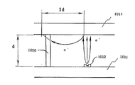
次に、図15を参照して、電位を規定する範囲2dについて説明する。
【0158】
メタルバック1019あるいはITO薄膜とリアプレート基板1011に印加される電位差をVa、間隔をdとする。電子源から放出された電子の一部が蛍光体で反射したり、蛍光体から陽イオンが放出され、近傍のスペーサ、蛍光体、電子源基板に照射される。蛍光体で反射された電子が、Va(eは電子の有する電荷)のエネルギーを持っていた場合、反射後に周辺に飛散する領域は蛍光体の前記反射位置から2dの範囲である。その範囲で、照射された部材が絶縁性の場合帯電が生じる。
【0159】
その領域に配置された部材に、高抵抗膜を施し帯電を防止した。
【0160】
ただし、2dよりも外側では帯電の影響は小さいため、不要なリーク電流を抑えるため絶縁性のスペーサCを使用した。
【0161】
【実施例】
[実施例]
図16は、本発明の画像形成装置の実施例の一部を破断した斜視図であり、図17は図16に示した画像形成装置Y方向から見た断面(AA′)を模式的に示した図である。図16、図17においてリアプレート(E11)には、複数の表面伝導型の電子放出素子(E12)がマトリックス上に配列された電子源(E13)が固定されている。電子源(E13)にはガラス基板(E14)の内面に蛍光膜(E15)と加速電極であるメタルバック(E16)が形成された、画像形成部材としてのフェースプレート(E17)が絶縁性材料からなる支持枠(E18)を介して対向配置されており、電子源(E13)とメタルバック(E16)との間には、不図示の電源により高電圧が印加される。これらリアプレート(E11)と支持枠(E18)およびフェースプレート(E17)とで外囲器を構成する。
【0162】
図15に示すように、メタルバック(E16)と電子源(E13)との間の距離をdとし、電子源から放出される電子がフェースプレートに入射する範囲をAとする。そのAの範囲に配置されるスペーサA(E19A)、その外郭から2d外側までの範囲に配置されるスペーサB(E19B)、さらにその外側にスペーサC(E19C)が配置される構成について説明する。
【0163】
スペーサ(E19A、E19B)には、表面に導電性を付与し帯電を抑止する。表面に導電膜(E111)として、SiO 2 を蒸着によって1000Å程度成膜した。表面抵抗の大きさは、1.0×10¹⁰(Ω/□)とした。
【0164】
また、電子源(E13)の表面には各電子放出素子(E12)およびそれらを電気的に接続する配線をのぞく部位の所定の範囲(E112)に金属膜からなる電位規定膜が形成され、この範囲内が電位規定部となっている。本実施例では、Ptのスパッタ膜を2000Å成膜することにより形成した。この電位規定膜は電子源近接領域(電子源の外周)のみ形成してもよい。
【0165】
さらに、フェースプレート(E17)の画像が表示される領域の外側にもITO膜(E110)、メタルバック(E16)などの膜が形成され電位規定されている。本実施例では、ITO(E110)を電位規定に用いた。
【0166】
なお、電位規定されない領域に配置されているスペーサCは、絶縁性の部材を使用した。
【0167】
本実施例では、dは5mmとした。すなわち電位規定される領域Bは、X方向、Y方向それぞれについて、画像表示領域から外側に約10mmの範囲である。画像表示時には、フェースプレート(E17)、リアプレート(E11)の間に6kVを印加した。素子の駆動のための電圧は15Vとした。
【0168】
電子放出素子(E12)から放出された電子がフェースプレート(E17)で反射されスペーサA、スペーサBに入射する。スペーサ表面では入射する電子によって、二次電子放出が生じて帯電が起きる。しかし、フェースプレート(E17)とリアプレート(E11)の電位規定された膜を通じてスペーサA、B表面の導電膜に微少電流が流れ、帯電を緩和することができる。
【0169】
また、素子駆動時にスペーサA、Bで発生するような帯電はスペーサCには発生しないので、素材を絶縁性としリーク電流を抑制することができる。
【0170】
その結果、電子源から放出された電子は帯電による影響を最小限に抑えられ、電子の軌道が安定し、発光位置ずれのない良好な画像を形成し、かつ帯電の影響を受けないスペーサでリーク電流を抑え消費電力を低減することができるようになった。
【0171】
なお、本実施例では、スペーサA、Bの表面抵抗を同じに設定したが、異なる抵抗値でもよい。特にスペーサBをAより高い抵抗にすることによりさらに消費電力を抑えることができる。
【0172】
[参考例]
本参考例では、画像表示領域内にスペーサが配置されるが、表示領域の周辺近傍にはスペーサが配置されない構成での説明を行なう。表示領域外の離れた場所にスペーサが配置されている。
【0173】
図18は、本発明の画像形成装置の参考例の一部を破断した斜視図であり、図19は図18に示した画像形成装置Y方向から見た断面(AA′)を模式的に示した図である。図19においてリアプレート(E21)には、複数の表面伝導型の電子放出素子(E22)がマトリックス上に配列された電子源(E23)が固定されている。電子源(E23)にはガラス基板(E24)の内面に蛍光膜(E25)と加速電極であるメタルバック(E26)が形成された、画像形成部材としてのフェースプレート(E27)が絶縁性材料からなる支持枠(E28)を介して対向配置されており、電子源(E23)とメタルバック(E26)との間には、不図示の電源により高電圧が印加される。これらリアプレート(E21)と支持枠(E28)およびフェースプレート(E27)とで外囲器を構成する。
【0174】
電子源から放出される電子がフェースプレートに入射する範囲をAとする。そのAの範囲に配置されるスペーサA(E29A)、さらにその外側にスペーサC(E29C)が配置される構成について説明する。
【0175】
この領域内に配置されるスペーサには、表面に導電膜(E111)をつけ導電性を付与し帯電を抑止する。表面にSiO 2 を蒸着によって1000Å程度成膜した。表面抵抗の大きさは、1.0×10¹⁰(Ω/□)とした。
【0176】
一方、画像表示領域外に配置されているスペーサは、絶縁性の部材を使用した。
【0177】
本実施例でも、dは5mmとした。画像表示時には、フェースプレート、リアプレートの間に6kVを印加した。素子の駆動のための電圧は15Vとした。
【0178】
画像表示領域内においては、画像表示時にスペーサの表面に帯電が生じたとき、フェースプレートとリアプレートの電位規定された膜を通じてスペーサ表面に微少電流が流れ、帯電を緩和することができる。画像領域外では、スペーサを絶縁とすることにより、リーク電流を抑制できる。
【0179】
【発明の効果】
以上説明した本発明によれば、画像領域内のスペーサの帯電による画質低下をおさえ、良好な画像を形成しつつリーク電流の小さく消費電力の小さい画像形成装置を提供することができる。
【図面の簡単な説明】
【図1】本発明の画像形成装置が備える表示パネルの斜視図
【図2】図1の表示パネルに用いたマルチ電子ビーム源の平面図
【図3】図2のマルチ電子ビーム源のB−B'に沿った断面図
【図4】蛍光体のレイアウト図
【図5】スペーサの拡大図
【図6】平面型の表面伝導型電子放出素子の平面図及び断面図
【図7】平面型の表面伝導型電子放出素子の製造工程図
【図8】フォーミング電圧の波形図
【図9】活性化処理用電源からの出力電圧の波形図
【図10】垂直型の表面伝導型電子放出素子の断面図
【図11】垂直型の表面伝導型電子放出素子の製造工程図
【図12】実施例で用いた表面伝導型電子放出素子の典型的な特性を示すグラフ
【図13】テレビジョン表示を行うための駆動回路
【図14】図1の画像形成装置のA−A 'に沿った断面図
【図15】電位を規定する範囲を説明するための電子放出素子付近の拡大断面図
【図16】実施例の斜視図
【図17】図16の実施例のA−A'に沿った断面図
【図18】参考例の斜視図
【図19】図18の参考例のA−A'に沿った断面図
【図20】従来の表面伝導型電子放出素子の平面図
【図21】従来の電界放出型素子の断面図
【図22】従来の金属/絶縁層/金属型電子放出素子の断面図
【図23】従来の平面型表示パネルの斜視図
【符号の説明】
1 絶縁性部材
3 当接面
5 側面部
11 高抵抗膜
21 低抵抗膜
22 凸部
31 境界膜
1010 黒色の導電体
1011 基板
1012 冷陰極素子
1013 行方向配線
1014 列方向配線
1015 リアプレート
1016 側壁
1017 フェースプレート
1018 蛍光膜
1019 メタルバック
1020 スペーサ
1101 基板
1102,1103 素子電極
1104 導電性薄膜
1105 電子放出部
1110 フォーミング用電源
1111 電流計
1112 活性化用電源
1113 通電活性化処理により形成した薄膜
1114 アノード電極
1115 直流高電圧電源
1116 電流計
1201 基板
1202,1203 素子電極
1204 導電性薄膜
1205 電子放出部
1206 段差形成部材
1213 通電活性化処理により形成した薄膜
1701 表示パネル
1702 走査回路
1703 制御回路
1704 シフトレジスタ
1705 ラインメモリ
1706 同期信号分離回路
1707 変調信号発生器
3001 基板
3004 導電性薄膜
3005 電子放出部
3010 基板
3011 エミッタ配線
3012 エミッタコーン
3013 絶縁層
3014 ゲート電極
3020 基板
3021 下電極
3022 絶縁層
3023 上電極
3111 基板
3112 冷陰極素子
3113 行方向配線
3114 列方向配線
3115 リアプレート
3116 側壁
3117 フェースプレート
3118 蛍光膜
3119 メタルバック
3120 スペーサ[0001]
BACKGROUND OF THE INVENTION
The present invention relates to an image forming apparatus, and more particularly to an image forming apparatus provided with an inner spacer in order to support atmospheric pressure applied to the outer envelope of the apparatus from the inside of the outer envelope.
[0002]
[Prior art]
Conventionally, two types of electron-emitting devices, a hot cathode device and a cold cathode device, are known. Among these, as the cold cathode device, for example, a surface conduction electron-emitting device, a field emission device (hereinafter referred to as FE type), a metal / insulating layer / metal-type emitting device (hereinafter referred to as MIM type), and the like are known. ing.
[0003]
Examples of surface conduction electron-emitting devices include M.I. I. Elinson, Radio Eng. Electron Phys. , 10, 1290, (1965) and other examples described later.
[0004]
The surface conduction electron-emitting device utilizes a phenomenon in which electron emission occurs when a current flows in parallel to a film surface of a small-area thin film formed on a substrate. As this surface conduction electron-emitting device, Sn by Erinson et al.O 2 In addition to thin film, Au thin film [G. Dittmer: “Thin SolidFilms”, 9, 317 (1972)],In 2 O 3 / SnO 2 By thin film [M. Hartwell and C.H. G. Fonstad: “IEEE Trans. ED Conf.”, 519 (1975)], carbon thin film [Hisa Araki et al .: Vacuum, Vol. 26, No. 1, 22 (1983)] and the like have been reported.
[0005]
As a typical example of the device configuration of these surface conduction electron-emitting devices, the above-described M.P. FIG. 3 shows a plan view of a device by Hartwell et al. In the figure,
[0006]
M.M. In the above-described surface conduction electron-emitting devices such as the device by Hartwell et al., It is common to form the electron-emitting
[0007]
An example of the FE type is, for example, W.W. P. Dyke & W. W. Dolan, “Field emission”, Advance in ElectroPhysics, 8, 89 (1956), or C.I. A. Spindt, “Physical properties of thin-film field emissions with molecondens cones”, J. Am. Appl. Phys. 47, 5248 (1976).
[0008]
As a typical example of the element configuration of the FE type, the above-described C.I. A. A cross-sectional view of the element according to Spindt et al. Is shown. In this figure, 3010 is a substrate, 3011 is an emitter wiring made of a conductive material, 3012 is an emitter cone, 3013 is an insulating layer, and 3014 is a gate electrode. This element causes field emission from the tip of the
[0009]
As another element configuration of the FE type, there is an example in which an emitter and a gate electrode are arranged on a substrate substantially parallel to the substrate plane, instead of the laminated structure as shown in FIG.
[0010]
Examples of the MIM type include C.I. A. Mead, “Operation of tunnel-emission Devices”, J. Am. Appl. Phys. , 32, 646 (1961) and the like are known. A typical example of the MIM type element configuration is shown in FIG. This figure is a sectional view, in which 3020 is a substrate, 3021 is a lower electrode made of metal, 3022 is a thin insulating layer having a thickness of about 100 angstroms, and 3023 is made of a metal having a thickness of about 80 to 300 angstroms. Electrode.
[0011]
In the MIM type, an appropriate voltage is applied between the upper electrode 3023 and the
[0012]
Since the above-described cold cathode device can obtain electron emission at a lower temperature than a hot cathode device, a heater for heating is not required. Therefore, the structure is simpler than that of the hot cathode device, and a fine device can be produced. Further, even if a large number of elements are arranged on the substrate at a high density, problems such as thermal melting of the substrate hardly occur. Further, unlike the case where the hot cathode element operates by heating of the heater, the response speed is slow. In the case of the cold cathode element, there is also an advantage that the response speed is fast.
[0013]
For this reason, research for applying cold cathode devices has been actively conducted.
[0014]
For example, a surface conduction electron-emitting device has an advantage that a large number of devices can be formed over a large area because it is particularly simple in structure and easy to manufacture among cold cathode devices. Therefore, for example, as disclosed in Japanese Patent Application Laid-Open No. 64-31332 by the present applicant, a method for arranging and driving a large number of elements has been studied.
[0015]
As for applications of surface conduction electron-emitting devices, for example, image forming apparatuses such as image display apparatuses and image recording apparatuses, charged beam sources, and the like have been studied.
[0016]
In particular, as an application to an image display device, for example, as disclosed in USP 5,066,883, Japanese Patent Application Laid-Open No. 2-257551 and Japanese Patent Application Laid-Open No. 4-28137 by the present applicant, An image display device using a combination of an emission element and a phosphor that emits light when irradiated with an electron beam has been studied. An image display device using a combination of a surface conduction electron-emitting device and a phosphor is expected to have characteristics superior to those of other conventional image display devices. For example, it can be said that it is superior in that it does not require a backlight and has a wide viewing angle as compared with a liquid crystal display device that has been widespread in recent years.
[0017]
A method for driving a plurality of FE types in a row is disclosed, for example, in USP 4,904,895 by the present applicant. As an example of applying the FE type to an image display device, for example, R.I. A flat panel display device reported by Meyer et al. Is known. [R. Meyer: “Recent Development on Microtips Display at LETI”, Tech. Digest of 4th Int. Vacuum Microele-tronics Conf. , Nagahama, pp. 6-9 (1991)]
An example in which a large number of MIM types are arranged and applied to an image display device is disclosed in, for example, Japanese Patent Application Laid-Open No. 3-55738 by the present applicant.
[0018]
Among the image forming apparatuses using the electron-emitting devices as described above, a flat-type display device with a small depth is attracting attention as a replacement for a CRT type display device because it is space-saving and lightweight.
[0019]
FIG. 23 is a perspective view showing an example of a display panel portion constituting a flat type image display device, and a part of the panel is cut away to show the internal structure.
[0020]
In the figure, 3115 is a rear plate, 3116 is a side wall, and 3117 is a face plate. The
[0021]
A
[0022]
A
[0023]
Dx1 to Dxm and Dy1 to Dyn and Hv are electrical connection terminals having an airtight structure provided to electrically connect the display panel and an electric circuit (not shown). Dx1 to Dxm are electrically connected to the
[0024]
Further, the inside of the hermetic container is maintained at a vacuum of about 10 to the sixth power of Torr, and as the display area of the image display device increases, the
[0025]
In the image display device using the display panel described above, when a voltage is applied to each
[0026]
The electron beam apparatus of the image forming apparatus described above has an envelope, an electron source, and an electron irradiation member for maintaining a vacuum atmosphere in the apparatus, and further, an atmospheric pressure applied to the envelope is supplied from the inside of the envelope. A spacer for supporting is arranged in the envelope.
[0027]
In particular, in the image forming apparatus such as the display apparatus described above, in order to realize a large area of the image display apparatus and a thinning of the apparatus, it is indispensable to arrange a spacer inside the envelope.
[0028]
[Problems to be solved by the invention]
However, when the spacer is arranged in the image forming apparatus, there is a problem that the irradiation position of the electron beam on the electron irradiation surface is deviated from the design position. In this case, for example, it means a deviation from the design value of the irradiation position of the electron beam or the light emission shape on the phosphor surface. In particular, when an image forming member provided with RGB phosphors for color images is used sometimes, a decrease in luminance or color shift may be observed along with the irradiation position of the electron beam. This phenomenon occurs particularly in the vicinity of the electron source, the image forming member, and spacers arranged in the vicinity thereof.
[0029]
The cause of this phenomenon is as follows.
[0030]
When electrons emitted from the electron source are irradiated on the irradiation member, a phenomenon occurs in which a part of the electrons is reflected by the irradiation member and ions are emitted from the irradiation member by the electron irradiation. The emitted electrons and ions cause charging of the insulating member when an insulating member is present in the vicinity. There are adhesion of radiated electrons and ions to an insulator, and charging due to generation of secondary electrons by rushing of the radiated electrons into the insulator.
[0031]
As the charging of the insulator proceeds, the surrounding electric field changes, and is then emitted from the electron source to cause a shift in the electron trajectory. As a result, there are problems such that electrons are not incident on the phosphor to emit light and other phosphors emit light.
[0032]
Not only the insulator disposed in the image display area, but also the insulator portion in the vicinity of the image display area is charged, causing a shift of the electron trajectory.
[0033]
SUMMARY OF THE INVENTION Accordingly, an object of the present invention is to prevent a positional deviation of an electron beam that occurs in an irradiation member of an electron source in the entire area and prevent a decrease in luminance and a color deviation in an image forming apparatus.
[0034]
[Means for Solving the Problems]
Electron emitterHaveElectron sourceWas placedElectron source areaRear plate withAnd to irradiate the electrons emitted from the electron source,Accelerating voltage for accelerating electrons emitted from the electron-emitting device, which are arranged opposite to the electron source in a vacuum atmosphere.Irradiation member region where electron irradiation member to which is applied is arrangedHaveFace plateAnd saidRear plateAnd saidFace platePlaced betweenAn envelope including a support frame, and a plurality of the envelopes disposed inside the envelopeIn an image forming apparatus having a spacer,Of the plurality of spacers, if the distance between the rear plate and the face plate is d, the electron source region and the adjacent region in the range of 2d from the outer periphery of the electron source region, or the irradiation member region and the The spacers disposed in the adjacent region within the range of 2d from the outer periphery of the irradiation member region are conductive, and the spacers disposed in the region other than the region are insulative.
[0035]
DETAILED DESCRIPTION OF THE INVENTION
Embodiments of the present invention will be described below with reference to the drawings.
[0036]
FIG. 1 is a perspective view of a display panel provided in the image forming apparatus of the present invention, and a part of the panel is cut away to show the internal structure.
[0037]
In the figure, 1015 is a rear plate, 1016 is a side wall, 1017 is a face plate, and 1015 to 1017 form an airtight container for maintaining the inside of the display panel in a vacuum. When assembling an airtight container, it is necessary to seal the joints of each member in order to maintain sufficient strength and airtightness. For example, frit glass is applied to the joints, and in the air or in a nitrogen atmosphere, Celsius. Sealing was achieved by baking at 400 to 500 degrees for 10 minutes or more. A method for evacuating the inside of the hermetic container will be described later. In addition, since the inside of the airtight container is maintained in a vacuum of about 10 to the sixth power [Torr], for the purpose of preventing destruction of the airtight container due to atmospheric pressure or unexpected impact, as an atmospheric pressure resistant structure, A
[0038]
Next, an electron-emitting device substrate that can be used in the image forming apparatus of the present invention will be described. The electron source substrate used in the image forming apparatus of the present invention is formed by arranging a plurality of cold cathode elements on the substrate.
[0039]
The cold cathode element arrangement method includes a ladder arrangement in which cold cathode elements are arranged in parallel and both ends of each element are connected by wiring (hereinafter referred to as a ladder arrangement electron source substrate), A simple matrix arrangement (hereinafter referred to as a matrix-type arrangement electron source substrate) in which a pair of element electrodes are connected to each other in the X-direction wiring and the Y-direction wiring is exemplified. An image forming apparatus having a ladder-type arrangement electron source substrate requires a control electrode (grid electrode) that is an electrode for controlling the flight of electrons from the electron-emitting device.
[0040]
A
[0041]
The multi-electron beam source used in the image display apparatus of the present invention is not limited in the material, shape, or manufacturing method of the cold cathode element as long as the cold cathode element is an electron source having a simple matrix wiring or ladder arrangement.
[0042]
Therefore, for example, a cold cathode device such as a surface conduction electron-emitting device, FE type, or MIM type can be used.
[0043]
Next, the structure of a multi-electron beam source in which surface conduction electron-emitting devices as cold cathode devices are arranged on a substrate and wired in a simple matrix will be described.
[0044]
FIG. 2 is a plan view of the multi-electron beam source used in the display panel of FIG. On the
[0045]
A cross section taken along the line BB 'of FIG. 2 is shown in FIG.
[0046]
The multi-electron source having such a structure has a row-
[0047]
In the present embodiment, the multi-electron
[0048]
A
[0049]
In addition, the method of separately applying the phosphors of the three primary colors is not limited to the stripe arrangement shown in FIG. 4A. For example, the delta arrangement shown in FIG. It may be an array.
[0050]
Note that when a monochrome display panel is formed, a monochromatic phosphor material may be used for the
[0051]
Further, a metal back 1019 known in the field of CRT is provided on the surface of the
[0052]
Further, for the purpose of applying an acceleration voltage or improving the conductivity of the fluorescent film, a transparent electrode made of, for example, ITO may be provided between the
[0053]
The spacer disposed in the image display area will be described. FIG. 5 is a schematic cross-sectional view of an enlarged portion of the AA ′
[0054]
The
[0055]
Examples of the insulating
[0056]
The
[0057]
The thickness t of the antistatic film formed on the insulating material is preferably in the range of 10 nm to 1 μm. Although it varies depending on the surface energy of the material, adhesion to the substrate, and substrate temperature, a thin film of 10 nm or less is generally formed in an island shape, and its resistance is unstable and reproducibility is poor. On the other hand, when the film thickness t is 1 μm or more, the film stress increases, the risk of film peeling increases, and the film formation time increases, resulting in poor productivity. Therefore, the film thickness is desirably 50 to 500 nm. The surface resistance R / □ is ρ / t, and the specific resistance ρ of the antistatic film is preferably 0.1 [Ωcm] to 10 8 [Ωcm] from the preferable range of R □ and t described above. . Furthermore, in order to realize a more preferable range of surface resistance and film thickness, ρ is preferably set to 10 2 to 10 6 Ωcm.
[0058]
As described above, the temperature of the spacer rises when a current flows through the antistatic film formed thereon or when the entire display generates heat during operation. When the resistance temperature coefficient of the antistatic film is a large negative value, the resistance value decreases when the temperature rises, the current flowing through the spacer increases, and the temperature rises further. The current continues to increase until it exceeds the power supply limit. The value of the resistance temperature coefficient at which such a current runaway occurs is empirically a negative value and the absolute value is 1% or more. That is, the resistance temperature coefficient of the antistatic film is desirably less than −1%.
[0059]
As a material of the
[0060]
As another material of the
[0061]
The alloy nitride film is formed on the insulating member by thin film forming means such as sputtering, reactive sputtering in a nitrogen gas atmosphere, electron beam vapor deposition, ion plating, or ion assist vapor deposition. The metal oxide film can also be produced by a similar thin film formation method, but in this case, oxygen gas is used instead of nitrogen gas. In addition, a metal oxide film can be formed by a CVD method or an alkoxide coating method. The carbon film is produced by vapor deposition, sputtering, CVD, or plasma CVD. In particular, when producing amorphous carbon, the atmosphere during film formation should contain hydrogen or be used as a film formation gas. Use hydrocarbon gas.
[0062]
The
[0063]
The
[0064]
As already described, the
[0065]
Electrons emitted from the
[0066]
Electrons emitted from the
[0067]
The
[0068]
The
[0069]
Dx1 to Dxm and Dy1 to Dyn and Hv are electrical connection terminals having an airtight structure provided for electrically connecting the display panel and an electric circuit (not shown). Dx1 to Dxm are electrically connected to the row-
[0070]
Further, in order to evacuate the inside of the hermetic container to a vacuum, after assembling the hermetic container, an unillustrated exhaust pipe and a vacuum pump are connected, and the inside of the hermetic container has a degree of vacuum of about 10 to the seventh power [Torr]. Exhaust. Thereafter, the exhaust pipe is sealed. In order to maintain the degree of vacuum in the hermetic container, a getter film (not shown) is formed at a predetermined position in the hermetic container immediately before or after sealing. The getter film is, for example, a film formed by heating and vapor-depositing a getter material mainly composed of Ba by a heater or high-frequency heating, and the inside of the hermetic container is 1 × 10 minus 5 to 1 or 1 by the adsorption action of the getter film. The degree of vacuum is maintained at x10 minus 7 [Torr].
[0071]
In the image display device using the display panel described above, electrons are emitted from each
[0072]
Usually, the voltage applied to 1012 to the surface conduction electron-emitting device of the present invention, which is a cold cathode device, is about 12 to 16 [V], and the distance d between the metal back 1019 and the
[0073]
The basic configuration and manufacturing method of the display panel of the present invention and the outline of the image display device have been described above.
[0074]
Next, the manufacturing method of the multi electron beam source used for the display panel will be described. The multi-electron beam source used in the image display apparatus of the present invention is not limited in the material, shape or manufacturing method of the cold cathode element as long as it is an electron source in which cold cathode elements are wired in a simple matrix. Therefore, for example, a cold cathode device such as a surface conduction electron-emitting device, FE type, or MIM type can be used.
[0075]
However, a surface conduction electron-emitting device is particularly preferable among these cold cathode devices under a situation where a display device having a large display screen and a low price is required. That is, in the FE type, the relative position and shape of the emitter cone and the gate electrode greatly affect the electron emission characteristics, and thus an extremely accurate manufacturing technique is required. This achieves a large area and a reduction in manufacturing cost. This is a disadvantageous factor. Further, in the MIM type, it is necessary to make the insulating layer and the upper electrode thin and uniform, but this is also a disadvantageous factor in achieving a large area and a reduction in manufacturing cost. In that respect, since the surface conduction electron-emitting device is relatively simple to manufacture, it is easy to increase the area and reduce the manufacturing cost. The inventors have also found that among surface conduction electron-emitting devices, those in which the electron-emitting portion or its peripheral portion is formed of a fine particle film are particularly excellent in electron-emitting characteristics and can be easily manufactured. Therefore, it can be said that it is most suitable for use in a multi-electron beam source of a high-luminance and large-screen image display device. Therefore, in the display panel of the above embodiment, a surface conduction electron-emitting device in which the electron emitting portion or its peripheral portion is formed of a fine particle film is used. First, the basic configuration, manufacturing method, and characteristics of a suitable surface conduction electron-emitting device will be described, and then the structure of a multi-electron beam source in which a number of devices are simply matrix-wired will be described.
[0076]
(Suitable device structure and manufacturing method of surface conduction electron-emitting device)
There are two types of typical structures of the surface conduction electron-emitting device in which the electron-emitting portion or its peripheral portion is formed of a fine particle film, a planar type and a vertical type.
[0077]
(Plane type surface conduction electron-emitting device)
First, the device configuration and manufacturing method of a planar surface conduction electron-emitting device will be described.
[0078]
FIG. 6 shows a plan view (a) and a cross-sectional view (b) for explaining the configuration of a planar surface conduction electron-emitting device. In the figure, 1101 is a substrate, 1102 and 1103 are element electrodes, 1104 is a conductive thin film, 1105 is an electron emission portion formed by energization forming treatment, and 1113 is a thin film formed by energization activation treatment.
[0079]
As the
[0080]
In addition,
[0081]
The shapes of the
[0082]
A fine particle film is used for the conductive
[0083]
The particle diameter of the fine particles used for the fine particle film is in the range of several angstroms to several thousand angstroms, and the preferred one is in the range of 10 angstroms to 200 angstroms. The film thickness of the fine particle film is appropriately set in consideration of various conditions as described below. That is, the condition necessary for electrically connecting to the
[0084]
Examples of materials that can be used to form the fine particle film include Pd, Pt, Ru, Ag, Au, Ti, In, Cu, Cr, Fe, Zn, Sn, Ta, W, and Pb. Starting metals, PdO, SnO 2 ,In 2 O 3, PbO,Sb 2 O 3 , And other oxides, and HfB 2, ZrB 2 , LaB 6 , CeB 6 , YB 4 , GdB 4 , Borides such as TiC, ZrC, HfC, TaC, SiC, WC, etc., nitrides such as TiN, ZrN, HfN, etc., Si, Ge, etc. And the like, carbon, and the like, which are appropriately selected from these.
[0085]
As described above, the conductive
[0086]
Note that it is desirable that the conductive
[0087]
In addition, the
[0088]
The
[0089]
The
[0090]
The basic configuration of the preferred element has been described above. In the examples, the following elements were used.
[0091]
That is, blue plate glass was used for the
[0092]
Pd or PdO was used as a main material of the fine particle film, the thickness of the fine particle film was about 100 [angstrom], and the width W was 100 [micrometer].
[0093]
Next, a preferred method for manufacturing a planar surface conduction electron-emitting device will be described.
[0094]
7A to 7D are cross-sectional views for explaining the manufacturing process of the surface conduction electron-emitting device, and the notations of the respective members are the same as those in FIG.
[0095]
1) First, as shown in FIG. 7A,
[0096]
In the formation, the
[0097]
2) Next, a conductive
[0098]
In forming the film, first, an organic metal solution is applied to the substrate (a), dried, heated and fired to form a fine particle film, and then patterned into a predetermined shape by photolithography and etching. Here, the organometallic solution is a solution of an organometallic compound whose main element is a fine particle material used for the conductive thin film. (Specifically, Pd was used as the main element in this example. Also, in this example, the dipping method was used as the coating method, but other methods such as spinner method and spray method may be used.)
In addition, as a method for forming a conductive thin film made of a fine particle film, for example, a vacuum evaporation method, a sputtering method, a chemical vapor deposition method, or the like other than the method by application of an organometallic solution used in this embodiment is used. Sometimes used.
[0099]
3) Next, as shown in FIG. 5C, an appropriate voltage is applied between the forming
[0100]
The energization forming process is a process in which a conductive
[0101]
In order to describe the energization method in more detail, FIG. 8 shows an example of an appropriate voltage waveform applied from the forming
[0102]
In the embodiment, for example, in a vacuum atmosphere of about 10 to the fifth power [torr], for example, the pulse width T1 is set to 1 [millisecond], the pulse interval T2 is set to 10 [milliseconds], and the peak value Vpf is set for each pulse. The voltage was increased by 0.1 [V]. The monitor pulse Pm was inserted at a rate of once every time 5 pulses of the triangular wave were applied. The monitor pulse voltage Vpm was set to 0.1 [V] so as not to adversely affect the forming process. Then, when the electrical resistance between the
[0103]
The above method is a preferred method for the surface conduction electron-emitting device of the present embodiment. For example, when the design of the surface conduction electron-emitting device such as the material and film thickness of the fine particle film or the device electrode interval L is changed. Therefore, it is desirable to change the energization conditions accordingly.
[0104]
4) Next, as shown in FIG. 7D, an appropriate voltage is applied between the
[0105]
The energization activation process is a process of energizing the
[0106]
Specifically, by applying a voltage pulse periodically in a vacuum atmosphere within a range of 10 minus 4 to 10 minus 5 [torr], an organic compound existing in the vacuum atmosphere originates. Deposit carbon or carbon compounds. The
[0107]
In order to describe the energization method in more detail, FIG. 9A shows an example of an appropriate voltage waveform applied from the
[0108]
[0109]
FIG. 9B shows an example of the emission current Ie measured by the
[0110]
The energization conditions described above are preferable conditions for the surface conduction electron-emitting device of this example. When the design of the surface conduction electron-emitting device is changed, it is desirable to change the conditions accordingly. .
[0111]
As described above, the planar surface conduction electron-emitting device shown in FIG.
[0112]
(Vertical surface conduction electron-emitting devices)
Next, another typical configuration of the surface conduction electron-emitting device in which the electron emission portion or its periphery is formed of a fine particle film, that is, the configuration of a vertical surface conduction electron-emitting device will be described.
[0113]
FIG. 10 is a schematic cross-sectional view for explaining the basic structure of a vertical type, in which 1201 is a substrate, 1202 and 1203 are element electrodes, 1206 is a step forming member, and 1204 is a conductive film using a fine particle film. 1205 is an electron emission portion formed by energization forming treatment, and 1213 is a thin film formed by energization activation treatment.
[0114]
The vertical type is different from the planar type described above in that one of the element electrodes (1202) is provided on the
[0115]
Next, a method for manufacturing a vertical surface conduction electron-emitting device will be described. 11A to 11F are cross-sectional views for explaining the manufacturing process, and the notation of each member is the same as in FIG.
[0116]
1) First, as shown in FIG. 11A, an
[0117]
2) Next, as shown in FIG. 2B, an insulating layer for forming a step forming member is laminated. The insulating layer is, for example, SiO 2 May be laminated by sputtering, but other film forming methods such as vacuum deposition and printing may be used.
[0118]
3) Next, as shown in FIG. 3C, the
[0119]
4) Next, as shown in FIG. 4D, a part of the insulating layer is removed by using, for example, an etching method to expose the
[0120]
5) Next, as shown in FIG. 5E, a conductive
[0121]
6) Next, as in the case of the planar type, an energization forming process is performed to form an electron emission portion. (The same process as the planar energization forming process described with reference to FIG. 7C may be performed.)
7) Next, as in the case of the planar type, an energization activation process is performed to deposit carbon or a carbon compound in the vicinity of the electron emission portion. (The same process as the planar energization activation process described with reference to FIG. 7D may be performed.)
As described above, the vertical surface conduction electron-emitting device shown in FIG.
[0122]
(Characteristics of surface conduction electron-emitting devices used in display devices)
The device configuration and manufacturing method of the planar and vertical surface conduction electron-emitting devices have been described above. Next, the characteristics of the devices used in the display device will be described.
[0123]
FIG. 12 shows typical examples of (emission current Ie) vs. (element applied voltage Vf) characteristics and (element current If) vs. (element applied voltage Vf) characteristics of the elements used in the display device. The emission current Ie is remarkably smaller than the device current If and is difficult to show on the same scale, and these characteristics are changed by changing design parameters such as the size and shape of the device. Therefore, the two graphs are shown in arbitrary units.
[0124]
The element used in the display device has the following three characteristics with respect to the emission current Ie.
[0125]
First, when a voltage greater than a certain voltage (referred to as a threshold voltage Vth) is applied to the device, the emission current Ie increases rapidly. On the other hand, at a voltage lower than the threshold voltage Vth, the emission current Ie hardly Not detected.
[0126]
That is, it is a nonlinear element having a clear threshold voltage Vth with respect to the emission current Ie.
[0127]
Second, since the emission current Ie changes depending on the voltage Vf applied to the device, the magnitude of the emission current Ie can be controlled by the voltage Vf.
[0128]
Third, since the response speed of the current Ie emitted from the element is high with respect to the voltage Vf applied to the element, the amount of electrons emitted from the element can be controlled by the length of time for which the voltage Vf is applied.
[0129]
Because of the above characteristics, the surface conduction electron-emitting device could be suitably used for a display device. For example, in a display device in which a large number of elements are provided corresponding to the pixels of the display screen, display can be performed by sequentially scanning the display screen by using the first characteristic. That is, a voltage equal to or higher than the threshold voltage Vth is appropriately applied to the driven element according to the desired light emission luminance, and a voltage lower than the threshold voltage Vth is applied to the non-selected element. By sequentially switching the elements to be driven, it is possible to display by sequentially scanning the display screen.
[0130]
Further, by using the second characteristic or the third characteristic, the light emission luminance can be controlled, so that gradation display can be performed.
[0131]
(Structure of multi-electron beam source with simple matrix wiring of many elements)
Next, the structure of a multi-electron beam source in which the above-described surface conduction electron-emitting devices are arranged on a substrate and wired in a simple matrix will be described.
[0132]
FIG. 2 is a plan view of the multi-electron beam source used in the display panel of FIG. A surface conduction electron-emitting device similar to that shown in FIG. 1 is arranged on the substrate, and these devices are wired in a simple matrix by row-
[0133]
A cross section taken along the line BB 'of FIG. 2 is shown in FIG.
[0134]
In addition, the multi-electron source having such a structure has a row-
[0135]
(Drive circuit configuration and drive method)
FIG. 13 is a block diagram showing a schematic configuration of a drive circuit for performing television display based on NTSC television signals. In the figure, a
[0136]
Hereinafter, functions of each part of the apparatus of FIG. 13 will be described in detail.
[0137]
First, the
[0138]
Next, the scanning circuit 1702 will be described. The circuit includes m switching elements (schematically shown by S1 to Sm in the drawing), and each switching element has an output voltage of a DC voltage source Vx or 0 [V] ( One of the ground levels is selected and electrically connected to the terminals Dx1 to Dxm of the
[0139]
The
[0140]
The
[0141]
The
[0142]
The modulation signal generator 1707 is a signal source for appropriately driving and modulating each of the electron-emitting
[0143]
As described with reference to FIG. 12, the surface conduction electron-emitting device according to the present invention has the following basic characteristics with respect to the emission current Ie. That is, there is a clear threshold voltage Vth (8 [V] in the case of a surface conduction electron-emitting device of an example described later) for electron emission, and electron emission occurs only when a voltage higher than the threshold Vth is applied. Further, for a voltage equal to or higher than the electron emission threshold, the emission current Ie also changes according to the voltage change as shown in the graph of FIG. For this reason, when a pulsed voltage is applied to the element, for example, no electron emission occurs even when a voltage equal to or lower than the electron emission threshold Vth is applied. An electron beam is output from the conduction electron-emitting device. At that time, the intensity of the output electron beam can be controlled by changing the pulse peak value Vm. Further, it is possible to control the total amount of charges of the output electron beam by changing the pulse width Pw.
[0144]
Therefore, a voltage modulation method, a pulse width modulation method, or the like can be adopted as a method for modulating the electron-emitting device in accordance with the input signal. When implementing the voltage modulation method, a voltage modulation method circuit is used as the modulation signal generator 1707, which generates a voltage pulse of a certain length and appropriately modulates the peak value of the pulse according to the input data. be able to. Further, when implementing the pulse width modulation method, the modulation signal generator 1707 generates a pulse pulse having a constant peak value, and appropriately modulates the width of the voltage pulse according to the input data. A circuit of the type can be used.
[0145]
The
[0146]
When the digital signal system is used, it is necessary to convert the output signal DATA of the synchronization
[0147]
In the case of a voltage modulation method using an analog signal, for example, an amplifier circuit using an operational amplifier or the like can be adopted as the modulation signal generator 1707, and a shift level circuit or the like can be added if necessary. In the case of the pulse width modulation method, for example, a voltage controlled oscillation circuit (VOC) can be adopted, and an amplifier for amplifying the voltage up to the driving voltage of the electron-emitting device can be added as necessary.
[0148]
In the image display apparatus to which the present invention can be applied, electron emission is generated by applying a voltage to each electron-emitting device via the external terminals Dox1 to Doxm and Doy1 to Doyn. A high voltage is applied to the metal back 1019 or transparent electrode (not shown) via the high voltage terminal Hv to accelerate the electron beam. The accelerated electrons collide with the
[0149]
The configuration of the image display apparatus described here is an example of an image forming apparatus to which the present invention can be applied, and various modifications can be made based on the idea of the present invention. The NTSC system is used as the input signal. However, the input signal is not limited to this, and other than the PAL and SECAM systems, the TV signal (high quality TV including the MUSE system) composed of a larger number of scanning lines than these. Can also be adopted.
[0150]
In the image display device of the present invention, a spacer for atmospheric pressure resistance is arranged in the display panel. As many spacers as necessary are arranged in the image display area and outside the area as needed.
[0151]
FIG. 14 is a cross-sectional view taken along the line AA ′ of the image forming apparatus of FIG. 1, and shows potential regulating portions of the spacer A (1020A), the spacer B (1020B), the spacer C (1020C), the face plate, and the rear plate.
[0152]
Therefore, the spacers A, B, and C arranged in the panel will be described.
[0153]
The spacer A in the image display region is provided with conductivity to withstand a high voltage applied between the metal back 1019 of the face plate 107 and the
[0154]
On the other hand, the spacer C outside the image area has a higher resistance than the spacer in the image area. In the region not affected by charging, it is not necessary to relax charging, and an insulating spacer C is used to suppress leakage current.
[0155]
In addition, the spacer B arranged outside the image display area in the range affected by charging imparts conductivity to the surface of the spacer. If the distance between the
[0156]
In that case, the potential is regulated in a range where the spacers having conductivity are arranged. The potential regulating portion 2000 of the
[0157]
Next, the range 2d that defines the potential will be described with reference to FIG.
[0158]
A potential difference applied to the metal back 1019 or the ITO thin film and the
[0159]
A high resistance film was applied to the member arranged in that region to prevent charging.
[0160]
However, since the influence of charging is small outside 2d, an insulating spacer C was used to suppress unnecessary leakage current.
[0161]
【Example】
[Example]
FIG. 16 shows an image forming apparatus of the present invention.Examples ofFIG. 17 is a diagram schematically showing a cross section (AA ′) viewed from the image forming apparatus Y direction shown in FIG. 16. 16 and 17, an electron source (E13) in which a plurality of surface conduction electron-emitting devices (E12) are arranged on a matrix is fixed to the rear plate (E11). In the electron source (E13), a face plate (E17) as an image forming member in which a fluorescent film (E15) and a metal back (E16) as an acceleration electrode are formed on the inner surface of a glass substrate (E14) is made of an insulating material. A high voltage is applied between the electron source (E13) and the metal back (E16) by a power source (not shown). The rear plate (E11), the support frame (E18), and the face plate (E17) constitute an envelope.
[0162]
As shown in FIG. 15, the distance between the metal back (E16) and the electron source (E13) is d, and the range in which the electrons emitted from the electron source are incident on the face plate is A. A configuration in which the spacer A (E19A) arranged in the range of A, the spacer B (E19B) arranged in the range from the outline to 2d outside, and the spacer C (E19C) arranged further outside will be described.
[0163]
The spacers (E19A, E19B) are imparted with conductivity on the surface to suppress charging. As a conductive film (E111) on the surface, SiO 2 Was deposited by evaporation to a thickness of about 1000 mm. The size of the surface resistance is 1.0 × 10¹⁰(Ω / □).
[0164]
Further, a potential regulating film made of a metal film is formed on the surface of the electron source (E13) in a predetermined range (E112) of a portion excluding each electron-emitting device (E12) and a wiring electrically connecting them. The range is the potential regulating portion. In the present example, a Pt sputtered film was formed by depositing 2000 mm. This potential regulating film may be formed only in the electron source proximity region (the outer periphery of the electron source).
[0165]
Further, a film such as an ITO film (E110) and a metal back (E16) is formed outside the region where the image of the face plate (E17) is displayed, and the potential is regulated. In this example, ITO (E110) was used for potential regulation.
[0166]
In addition, the spacer C arrange | positioned in the area | region where electric potential is not defined used the insulating member.
[0167]
In this embodiment, d is 5 mm. That is, the potential-defined region B is a range of about 10 mm outward from the image display region in each of the X direction and the Y direction. At the time of image display, 6 kV was applied between the face plate (E17) and the rear plate (E11). The voltage for driving the element was 15V.
[0168]
Electrons emitted from the electron-emitting device (E12) are reflected by the face plate (E17) and enter the spacers A and B. On the spacer surface, incident electrons cause secondary electron emission and charging occurs. However, a minute current flows through the conductive films on the surfaces of the spacers A and B through the potential-regulated films of the face plate (E17) and the rear plate (E11), so that charging can be alleviated.
[0169]
In addition, since charging that occurs in the spacers A and B when the element is driven does not occur in the spacer C, the material can be made insulative and leakage current can be suppressed.
[0170]
As a result, the electrons emitted from the electron source are minimized by the effects of charging, the electron trajectory is stable, a good image with no displacement of the light emission position is formed, and leakage occurs with spacers that are not affected by charging. It has become possible to reduce power consumption by suppressing current.
[0171]
In this embodiment, the surface resistances of the spacers A and B are set to be the same, but different resistance values may be used. In particular, the power consumption can be further suppressed by making the spacer B have a higher resistance than A.
[0172]
[Reference example]
BookReference exampleThen, although a spacer is arrange | positioned in an image display area, it demonstrates by the structure by which a spacer is not arrange | positioned in the periphery vicinity of a display area. Spacers are arranged at remote locations outside the display area.
[0173]
FIG. 18 shows an image forming apparatus according to the present invention.Reference exampleFIG. 19 is a diagram schematically showing a cross section (AA ′) viewed from the image forming apparatus Y direction shown in FIG. 18. In FIG. 19, an electron source (E23) in which a plurality of surface conduction electron-emitting devices (E22) are arranged on a matrix is fixed to the rear plate (E21). In the electron source (E23), a face plate (E27) as an image forming member in which a fluorescent film (E25) and a metal back (E26) as an acceleration electrode are formed on the inner surface of a glass substrate (E24) is made of an insulating material. A high voltage is applied between the electron source (E23) and the metal back (E26) by a power source (not shown). The rear plate (E21), the support frame (E28), and the face plate (E27) constitute an envelope.
[0174]
A range in which electrons emitted from the electron source are incident on the face plate is A. A configuration in which the spacer A (E29A) arranged in the range of A and the spacer C (E29C) arranged outside thereof will be described.
[0175]
The spacer disposed in this region is provided with a conductive film (E111) on the surface to impart conductivity and suppress charging. Si on the surfaceO 2 Was deposited by evaporation to a thickness of about 1000 mm. The size of the surface resistance is 1.0 × 10¹⁰(Ω / □).
[0176]
On the other hand, the spacer arrange | positioned out of the image display area used the insulating member.
[0177]
In this embodiment, d is 5 mm. At the time of image display, 6 kV was applied between the face plate and the rear plate. The voltage for driving the element was 15V.
[0178]
In the image display area, when charging occurs on the surface of the spacer during image display, a minute current flows through the spacer surface through the potential-regulated films of the face plate and the rear plate, and the charging can be relaxed. Outside the image region, the leakage current can be suppressed by insulating the spacer.
[0179]
【The invention's effect】
According to the present invention described above, it is possible to provide an image forming apparatus with low leakage current and low power consumption while suppressing the image quality deterioration due to the charging of the spacers in the image area while forming a good image.
[Brief description of the drawings]
FIG. 1 is a perspective view of a display panel provided in an image forming apparatus of the present invention.
2 is a plan view of a multi-electron beam source used in the display panel of FIG.
3 is a cross-sectional view of the multi-electron beam source of FIG. 2 along BB ′.
FIG. 4 is a layout diagram of phosphors.
[Fig. 5] Enlarged view of spacer
FIG. 6 is a plan view and a cross-sectional view of a planar surface conduction electron-emitting device.
FIG. 7 is a manufacturing process diagram of a planar surface conduction electron-emitting device.
FIG. 8 is a waveform diagram of the forming voltage.
FIG. 9 is a waveform diagram of an output voltage from a power supply for activation processing.
FIG. 10 is a sectional view of a vertical surface conduction electron-emitting device.
FIG. 11 is a manufacturing process diagram of a vertical surface conduction electron-emitting device.
FIG. 12 is a graph showing typical characteristics of the surface conduction electron-emitting device used in the examples.
FIG. 13 shows a driving circuit for performing television display.
14 is a diagram of the image forming apparatus of FIG.A-A 'Sectional view along
FIG. 15 is an enlarged cross-sectional view in the vicinity of an electron-emitting device for explaining a range defining a potential
FIG. 16ExamplePerspective view
17 is the same as FIG.ExampleSectional view along AA '
FIG. 18Reference examplePerspective view
19 is the same as FIG.Reference exampleSectional view along AA '
FIG. 20 is a plan view of a conventional surface conduction electron-emitting device.
FIG. 21 is a sectional view of a conventional field emission device.
FIG. 22 is a sectional view of a conventional metal / insulating layer / metal-type electron-emitting device.
FIG. 23 is a perspective view of a conventional flat display panel.
[Explanation of symbols]
1 Insulating material
3 Contact surface
5 Sides
11 High resistance film
21 Low resistance film
22 Convex
31 Boundary membrane
1010 Black conductor
1011 substrate
1012 Cold cathode device
1013 Row direction wiring
1014 Wiring in column direction
1015 Rear plate
1016 side wall
1017 Face plate
1018 Fluorescent film
1019 Metal back
1020 Spacer
1101 substrate
1102, 1103 Device electrode
1104 Conductive thin film
1105 Electron emission unit
1110 Power supply for forming
1111 Ammeter
1112 Power supply for activation
1113 Thin film formed by energization activation process
1114 Anode electrode
1115 DC high voltage power supply
1116 Ammeter
1201 substrate
1202, 1203 Device electrode
1204 conductive thin film
1205 electron emitter
1206 Step forming member
1213 Thin film formed by energization activation treatment
1701 Display panel
1702 Scanning circuit
1703 Control circuit
1704 Shift register
1705 line memory
1706 Sync signal separation circuit
1707 Modulation signal generator
3001 Substrate
3004 Conductive thin film
3005 Electron emitter
3010 substrate
3011 Emitter wiring
3012 Emitter cone
3013 Insulating layer
3014 Gate electrode
3020 substrate
3021 Lower electrode
3022 Insulating layer
3023 Upper electrode
3111 substrate
3112 Cold cathode element
3113 Row direction wiring
3114 Column wiring
3115 Rear plate
3116 side wall
3117 face plate
3118 phosphor film
3119 metal back
3120 Spacer
Claims (6)
前記複数のスペーサのうち、前記リアプレートと前記フェースプレートの間の距離をdとすると、前記電子源領域と前記電子源領域の外周から2dの範囲にある隣接領域、または前記照射部材領域と前記照射部材領域の外周から2dの範囲にある隣接領域に配置されたスペーサは、導電性であり、上記領域以外の領域に配置されたスペーサは絶縁性であることを特徴とする画像形成装置。A rear plate having an electron source region where the electron source is arranged to have an electron-emitting device, in order to irradiate the electrons emitted from the electron source, disposed opposite in a vacuum atmosphere to the electron source, the electron-emitting devices A face plate having an irradiation member region in which an electron irradiation member to which an acceleration voltage for accelerating electrons emitted from the electron beam is applied is disposed, and a support frame disposed between the rear plate and the face plate. In an image forming apparatus having an envelope provided, and a plurality of spacers arranged inside the envelope ,
Of the plurality of spacers, if the distance between the rear plate and the face plate is d, the electron source region and the adjacent region in the range of 2d from the outer periphery of the electron source region, or the irradiation member region and the An image forming apparatus , wherein a spacer disposed in an adjacent region within a range of 2d from the outer periphery of the irradiation member region is conductive, and a spacer disposed in a region other than the region is insulative .
Priority Applications (1)
| Application Number | Priority Date | Filing Date | Title |
|---|---|---|---|
| JP04920099A JP3624111B2 (en) | 1999-02-25 | 1999-02-25 | Image forming apparatus |
Applications Claiming Priority (1)
| Application Number | Priority Date | Filing Date | Title |
|---|---|---|---|
| JP04920099A JP3624111B2 (en) | 1999-02-25 | 1999-02-25 | Image forming apparatus |
Publications (2)
| Publication Number | Publication Date |
|---|---|
| JP2000251709A JP2000251709A (en) | 2000-09-14 |
| JP3624111B2 true JP3624111B2 (en) | 2005-03-02 |
Family
ID=12824367
Family Applications (1)
| Application Number | Title | Priority Date | Filing Date |
|---|---|---|---|
| JP04920099A Expired - Fee Related JP3624111B2 (en) | 1999-02-25 | 1999-02-25 | Image forming apparatus |
Country Status (1)
| Country | Link |
|---|---|
| JP (1) | JP3624111B2 (en) |
Families Citing this family (3)
| Publication number | Priority date | Publication date | Assignee | Title |
|---|---|---|---|---|
| JP3667301B2 (en) | 2001-06-15 | 2005-07-06 | キヤノン株式会社 | Vacuum container and method of manufacturing image forming apparatus using the vacuum container |
| JP4797423B2 (en) * | 2005-04-07 | 2011-10-19 | ソニー株式会社 | Flat panel display |
| KR20070103901A (en) * | 2006-04-20 | 2007-10-25 | 삼성에스디아이 주식회사 | Vacuum envelope and electron emission display device using the same |
-
1999
- 1999-02-25 JP JP04920099A patent/JP3624111B2/en not_active Expired - Fee Related
Also Published As
| Publication number | Publication date |
|---|---|
| JP2000251709A (en) | 2000-09-14 |
Similar Documents
| Publication | Publication Date | Title |
|---|---|---|
| JP3234188B2 (en) | Image forming apparatus and manufacturing method thereof | |
| JP3187367B2 (en) | Electronic device and image forming apparatus using the same | |
| JP3305252B2 (en) | Image forming device | |
| JP3195290B2 (en) | Image forming device | |
| JPH1116521A (en) | Electron device and image forming device using it | |
| JP3703287B2 (en) | Image forming apparatus | |
| EP0867911A1 (en) | Image forming apparatus and method of manufacturing the same | |
| JP3466870B2 (en) | Method of manufacturing image forming apparatus | |
| JP3302293B2 (en) | Image forming device | |
| JP4095195B2 (en) | Electron beam generator and image forming apparatus | |
| JP3624111B2 (en) | Image forming apparatus | |
| JP3639732B2 (en) | Spacer manufacturing method and image display device manufacturing method | |
| JP3619043B2 (en) | Image forming apparatus | |
| JP3768697B2 (en) | Image forming apparatus | |
| JP3581586B2 (en) | Method of manufacturing spacer and method of manufacturing electron beam device | |
| JP3728099B2 (en) | Antistatic film and display device | |
| JP3466868B2 (en) | Electron beam generator and image forming apparatus | |
| JP3230729B2 (en) | Electron beam apparatus, electron source and image forming apparatus using the same | |
| JPH10284284A (en) | Antistatic film and display device | |
| JP2000113997A (en) | Antistatic film, member, electron beam device using this member, and image forming device | |
| JP2000243319A (en) | Image forming device | |
| JPH1116519A (en) | Electron beam apparatus and image forming apparatus | |
| JPH11339696A (en) | Image forming device | |
| JP2000208072A (en) | Image forming device | |
| JP2000173510A (en) | Image formation device |
Legal Events
| Date | Code | Title | Description |
|---|---|---|---|
| A977 | Report on retrieval |
Free format text: JAPANESE INTERMEDIATE CODE: A971007 Effective date: 20040906 |
|
| A131 | Notification of reasons for refusal |
Free format text: JAPANESE INTERMEDIATE CODE: A131 Effective date: 20041008 |
|
| A521 | Written amendment |
Free format text: JAPANESE INTERMEDIATE CODE: A523 Effective date: 20041020 |
|
| TRDD | Decision of grant or rejection written | ||
| A01 | Written decision to grant a patent or to grant a registration (utility model) |
Free format text: JAPANESE INTERMEDIATE CODE: A01 Effective date: 20041111 |
|
| A61 | First payment of annual fees (during grant procedure) |
Free format text: JAPANESE INTERMEDIATE CODE: A61 Effective date: 20041129 |
|
| R150 | Certificate of patent or registration of utility model |
Free format text: JAPANESE INTERMEDIATE CODE: R150 |
|
| FPAY | Renewal fee payment (event date is renewal date of database) |
Free format text: PAYMENT UNTIL: 20081203 Year of fee payment: 4 |
|
| FPAY | Renewal fee payment (event date is renewal date of database) |
Free format text: PAYMENT UNTIL: 20091203 Year of fee payment: 5 |
|
| FPAY | Renewal fee payment (event date is renewal date of database) |
Free format text: PAYMENT UNTIL: 20091203 Year of fee payment: 5 |
|
| FPAY | Renewal fee payment (event date is renewal date of database) |
Free format text: PAYMENT UNTIL: 20101203 Year of fee payment: 6 |
|
| FPAY | Renewal fee payment (event date is renewal date of database) |
Free format text: PAYMENT UNTIL: 20111203 Year of fee payment: 7 |
|
| LAPS | Cancellation because of no payment of annual fees |