JP3740296B2 - Image forming apparatus - Google Patents
Image forming apparatus Download PDFInfo
- Publication number
- JP3740296B2 JP3740296B2 JP28576498A JP28576498A JP3740296B2 JP 3740296 B2 JP3740296 B2 JP 3740296B2 JP 28576498 A JP28576498 A JP 28576498A JP 28576498 A JP28576498 A JP 28576498A JP 3740296 B2 JP3740296 B2 JP 3740296B2
- Authority
- JP
- Japan
- Prior art keywords
- layer
- spacer
- film
- electron
- forming apparatus
- Prior art date
- Legal status (The legal status is an assumption and is not a legal conclusion. Google has not performed a legal analysis and makes no representation as to the accuracy of the status listed.)
- Expired - Fee Related
Links
Images


Description
【0001】
【発明の属する技術分野】
本発明は画像形成装置に関わり、特に複数の電子放出素子を配置した平面型画像形成装置に好適に用いられるものである。
【0002】
【従来の技術】
従来から、電子放出素子として熱陰極素子と冷陰極素子の2種類が知られている。このうち冷陰極素子では、たとえば表面伝導型電子放出素子や、電界放出型電子放出素子(以下FE型と記す)や、金属/絶縁層/金属型電子放出素子(以下MIM型と記す)、などが知られている。
【0003】
表面伝導型電子放出素子は、基板上に形成された小面積の薄膜に、膜面に平行に電流を流すことにより電子放出が生ずる現象を利用するものである。この表面伝導型放出素子としては、エリンソン等によるSnO2 薄膜を用いたもの[M.I.Elinson,Radio Eng.Electron Phys.,10,1290,(1965)]、Au薄膜によるもの[G.D Mitter:“Thin Solid Films",9,317(1972)]や、In2 O3/SnO2 薄膜によるもの[M.Hartwell And C.G.Fonstad:“IEEE Trans.ED Conf.",519(1975)]や、カーボン薄膜によるもの[荒木久 他:真空、第26巻、第1号、22(1983)]等が報告されている。
【0004】
これらの表面伝導型電子放出素子の素子構成の典型的な例として、図20に前述のM.Hartwellらによる素子の平面図を示す。同図において、1は基板で、2はスパッタで形成された金属酸化物よりなる導電性薄膜である。導電性薄膜2は図示のようにH字形の平面形状に形成されている。該導電性薄膜2に通電フォーミングと呼ばれる通電処理を施すことにより、電子放出部3が形成される。
【0005】
通電フォーミングは、前記導電性薄膜2の両端に一定の直流電圧、もしくは、例えば1V/分程度の非常にゆっくりとしたレートで昇圧する直流電圧を印加して通電し、導電性薄膜2を局所的に破壊もしくは変形もしくは変質せしめ、電気的に高抵抗な状態の電子放出部3を形成することである。尚、局所的に破壊もしくは変形もしくは変質した導電性薄膜2の一部には、亀裂が発生する。前記通電フォーミング後に導電性薄膜2に適宜の電圧を印加した場合には、前記亀裂付近において電子放出が行われる。
【0006】
FE型の例は、たとえば、W.P.Dyke&W.W.Dolan,“Field Emission",Advance in Electron Physics,8,89(1956)や、あるいは、C.A.Spindt,“Physical Properties of Thin-Film Field Emission cathodes with molybdenium Cones",J.Appl.Phys.,47,5248(1976)などが知られている。
【0007】
FE型の素子構成の典型的な例として、図21に前述のC.A.Spindtらによる素子の断面図を示す。同図において、4は基板で、5は導電材料よりなるエミッタ配線、6はエミッタコーン、7は絶縁層、8はゲート電極である。本素子は、エミッタコーン6とゲート電極8の間に適宜の電圧を印加することにより、エミッタコーン6の先端部より電界放出を起こさせるものである。
【0008】
また、FE型の他の素子構成として、図21のような積層構造以外に、基板上に基板平面とほぼ平行にエミッタとゲート電極を配置した例もある。
【0009】
MIM型の例としては、たとえば、C.A.Mead,“Operation of Tunnel-Emission Devices,J.Appl.Phys.,32,646(1961)などが知られている。MIM型の素子構成の典型的な例を図22に示す。同図は断面図であり、図において、9は基板で、10は金属よりなる下電極、11は厚さ100オングストローム程度の薄い絶縁層、12は厚さ80〜300オングストローム程度の金属よりなる上電極である。MIM型においては、上電極12と下電極10の間に適宜の電圧を印加することにより、上電極12の表面より電子放出を起こさせるものである。
【0010】
上述した各種冷陰極素子は、熱陰極素子と比較して低温で電子放出を得ることができるため、加熱用ヒーターを必要としない。したがって、熱陰極素子よりも構造が単純であり、微細な素子を作成可能である。また、基板上に多数の素子を高い密度で配置しても、基板の熱溶融などの問題が発生しにくい。また、熱陰極素子がヒーターの加熱により動作するため応答速度が遅いのとは異なり、冷陰極素子の場合には応答速度が速いという利点もある。
【0011】
上述した冷陰極素子の応用については、画像表示装置、画像記録装置などの画像形成装置や、荷電ビーム源等がある。
【0012】
特に冷陰極素子を画像表示装置へ応用した例として、本出願人によるUSP
5,066,833や特開平2−257551号公報や特開平4−28137号公報において開示されているように、表面伝導型放出素子と電子ビームの照射により発光する蛍光体とを組み合わせて用いた画像表示装置が研究されている。表面伝導型放出素子と、表面伝導型放出素子による電子ビームの照射により発光する蛍光体とを組み合わせて用いて発光する画像表示装置がある。
【0013】
また、FE型を多数個ならべて画像表示装置に応用した例として、R.Meyerらにより報告された平板型表示装置が知られている[R.Meyer:“Recent Development on Microchips Display at LETI",Tech.Digest of 4th Int.Vacuum Micro Electronics Conf.,Nagahama,pp.6〜9(1991)]。
【0014】
また、MIM型を多数個ならべて画像表示装置に応用した例は、本出願人による特開平3−55738号公報に開示されている。
【0015】
各冷陰極型の中でも表面伝導型電子放出素子は、構造が単純で製造も容易であることから、大面積に多数の素子を形成しやすい利点がある。
【0016】
表面伝導型電子放出素子と蛍光体とを組み合わせて用いた画像表示装置は、液晶表示装置と比較すると、自発光型であるためバックライトを必要としない点や、視野角が広い点が優れている。
【0017】
平面型画像表示装置は上述した電子放出素子を平面基板に多数配置し、これと対向して電子により発光する蛍光体が配置される。電子放出素子は基板に二次元マトリクス状に配列され(マルチ電子源と呼ぶ)、各素子は行方向配線と列方向配線に接続される。画像表示方式の一例として、以下の単純マトリクス駆動がある。
【0018】
マトリクス中の任意の一行から電子を放出させるためには、行方向に選択電圧を印加し、これと同期して列配線に信号電圧を印加する。
【0019】
選択された行の電子放出素子より放出した電子は蛍光体に向かって加速され、蛍光体を励起、発光させる。行方向に順次選択電圧を印加することにより画像が表示される。
【0020】
二次元マトリクス状に電子放出素子が形成された基板(リアプレート)と、蛍光体と加速電極が形成された基板(フェースプレート)間は真空に保たれる必要がある。リアプレートとフェースプレートには大気圧が加わるため、表示装置が大型化するに伴い、大気圧を支持する厚みの基板が必要となる。しかし、ガラス等の両基板の厚みを増加すれば、重量の増加を招くため、リアプレートとフェースプレート間に支持部材(スペーサ)を挿入することにより、軽量化できてリアプレートとフェースプレート間隔を一定に保つとともに、リアプレートとフェースプレートの破損を防ぐ構造が取られる。
【0021】
スペーサは大気圧に耐圧、支持するために十分な機械的強度が求められ、且つリアプレートとフェースプレート間を飛翔する電子の軌道に大きく影響してはならない。電子軌道に影響を与える原因はスペーサの帯電である。スペーサ帯電は電子源から放出した電子の一部あるいはフェースプレートで反射した電子がスペーサに入射し、スペーサから二次電子が放出されることにより、あるいは電子の衝突により電離したイオンが表面に付着することによるものと考えられる。
【0022】
スペーサが正帯電するとスペーサ近傍を飛翔する電子がスペーサに引き寄せられるため、スペーサ近傍で表示画像に歪みを生ずる。帯電の影響はリアプレートとフェースプレート間隔が大きくなるに従い顕著になる。
【0023】
一般に帯電を抑制する手段として、帯電面に導電性を付与し、若干の電流を流すことで電荷を除去することが行なわれる。この概念をスペーサに応用しスペーサ表面を酸化スズで被覆する手法が特開昭57−118355号公報に開示されている。また、特開平3−49135号公報にはPdO系ガラス材で被覆する手法が開示されている。
【0024】
また、画像表示装置として輝度が高いことは重要な要素である。フェースプレートに形成されている蛍光体を効率よく発光させるためには、高い電圧で加速した電子を蛍光体に照射すればよく、十分な効率で発光させるためには電子を3kV以上に、望ましくは5kV以上に加速するとよい。したがって、リアプレートとフェースプレート間には数kV以上の電圧が印加されていることになり、スペーサ両端にもこれとほぼ同電位の電圧が印加される。スペーサに使われる材料は加速電圧の印加において放電しないことが求められる。
【0025】
沿面放電耐圧の向上手段として、二次電子放出率が小さい材料で表面を被覆すると効果的である。二次電子放出率が小さい材料で被覆した例として、酸化クロム(T.S.Sudarshan and J.D.Cross:IEEE Tran.EI-11,32(1976))、酸化銅(J.D.Cross and T.S.sudarshan:IEEE Tran.EI-9146(1974))が知られている。
【0026】
【発明が解決しようとする課題】
しかしながら、上記の酸化物半導体材料をマルチ電子源を有する画像表示装置のスペーサに適応した場合、以下の点で十分な性能を発揮しない場合がある。すなわち酸化物半導体材料は固有抵抗値が低いため、極めて薄くコーティングしない限り、スペーサ表面を流れる電流が大きくありすぎる。抵抗値が低いと高加速電圧を使用する画像表示装置においては、スペーサ部の発熱が問題となる。また、酸化物半導体は雰囲気ガスにより抵抗値が大きく変化するためバラツキが大きく、非常に薄い薄膜での抵抗制御が困難であり、したがって再現よくスペーサを製造することができない。
【0027】
すなわち、スペーサあるいはその表面層の材質として好ましい物性についての予測はされていたが、マルチ電子源より放出した電子を3kV以上の電圧により加速し、これにより蛍光体を発光させる画像表示装置で代表される画像形成装置のスペーサとして適する材料がなかった。したがって高電圧により蛍光体を発光させることにより高輝度で歪みのない画像を形成する画像形成装置の実現が困難であった。
【0028】
本発明は、スペーサとして当該画像形成装置に適したスペーサの表面層の構造と材料を新規に提供し、高輝度で歪のない画像を表示できる画像形成装置を提供することを課題とする。
【0029】
【課題を解決するための手段】
本発明の画像形成装置は、電子を放出する電子源とプレートとをスペーサを介して対向させた構造を有する画像形成装置において、該スペーサは基材と、該基材表面を被覆する絶縁性膜からなる第一層と、該第一層を被覆する半導電性膜からなる第二層とを有し、前記第一層の一部が、前記第二層から複数箇所で島状に露出していることを特徴とする画像形成装置である。
【0031】
【発明の実施の形態】
本発明による実施形態について、図面を参照しつつ詳細に説明する。
【0032】
[表示パネルの説明]
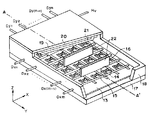
図1は本発明による実施形態の画像表示装置の応用例として表示パネルの斜視図であり、内部構造を示すためにパネルの一部を切り欠いて示している。図中、符号17はリアプレート、18は側壁、19はフェースプレートであり、符号17〜19により表示パネルの内部を真空に維持するための気密容器を形成している。気密容器を組み立てるにあたっては、各部材の接合部に十分な強度と気密性を保持させるため封着する必要があるが、例えばフリットガラスを各接合部に塗布し、大気中あるいは窒素雰囲気中で、摂氏400〜500℃で10分以上焼成することにより封着を達成した。気密容器内部を真空に排気する方法については後述する。また、上記気密容器の内部は10-4Pa 程度の真空に保持されるので、大気圧や不意の衝撃などによる気密容器の破壊を防止する目的で、耐大気圧構造体として、スペーサ22が設けられている。
【0033】
また、図1において、リアプレート17には、基板13を搭載し、基板13上に電子放出素子14と、該電子放出素子14の一方の電極に接続されたマトリクス状のX方向の配線15と、該電子放出素子14の他方の電極に接続されたY方向の配線16とが備えられ、フェースプレート19には、順次蛍光体20とメタルバック21とを備えており、各配線15,16に画像信号と走査信号を供給して、メタルバック21に高電圧HVを印加した場合に電子放出素子14からの電子を蛍光体20に照射して蛍光を発して、図1の上方向からの視認者に画像を表示することができる。
【0034】
[スペーサの構成と作用]
次に本発明を適用した画像表示装置の表示パネルに用いるスペーサの構成と作用について、具体的な例を示して説明する。
【0035】
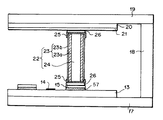
図2はスペーサ22を中心とした図1に示したA−A’線の表示装置断面模式図である。それぞれの番号は図1に対応している。図2において、符号14は冷陰極電子源を構成する電子放出素子、17はリアプレート、18は側壁、19はフェースプレートであり、符号17、18、19により表示パネルの内部を真空に維持するための気密容器を形成している。また、13は絶縁性基板、57は絶縁層、15はX方向配線、26は導電性材料を混入した接着材のフリットガラス、25は低抵抗材の導電膜、24はスペーサ22の絶縁性基材、23aは酸化物の絶縁性層である第一層、23bは高抵抗性材の第二層、21はメタルバック、20は蛍光体である。
【0036】
スペーサ22は外囲器内を真空にすることにより、大気圧を受けて、外囲器が破損あるいは変形するのを避けるために設けられる。スペーサ22の材質、形状、配置、配置本数等は外囲器の形状ならびに熱膨張係数等、外囲器の受ける大気圧、熱等を考慮して決定される。スペーサ22の形状には平板型、十字型、L字型、円筒形、電子通過孔を設けた平板形等がある。
【0037】
スペーサ22を構成する絶縁性基材24は電子放出素子14が形成されたリアプレート17、蛍光体20が形成されたフェースプレート19とほぼ同一の熱膨張特性の材料であることが必要である。あるいは、絶縁性基材24の弾性が高く、熱変形を容易に吸収するものであってもよい。フェースプレート19及びリアプレート17にかかる大気圧を支持する必要から、ガラス、セラミクス等機械的強度の高く、耐熱性の高い材料が適する。フェースプレート19、リアプレート17の材質としてガラスを用いた場合、表示装置作製行程中の熱応力を抑えるために、スペーサ22の絶縁性基材24はできるだけこれらの材質と同じものか、同様の熱膨張係数の材料であることが望ましい。
【0038】
本発明者らはスペーサ22の帯電を防止する方法を検討した結果、帯電を防止するために2次電子放出率が小さい特性を有する第一の膜23aの上に第二層23bとしてネットワーク構造または島状で、第一層23aが露出する構造の導電性を有する膜を形成することが有効であることを見出した。特に第一層23aとしてCr2 O3 、Nb2 O5 、Y2 O3 などの二次電子放出効率が小さい材料を含む組成の膜が極めて有効である。
【0039】
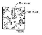
ここで、スペーサ22の第一の膜23aの上に第二層23bとしてネットワーク構造または島状構造の概略図を示して説明する。図3は、本発明の実施例で用いた第二層がネットワーク構造と島状の混合状態の構造であるスペーサ表面の拡大図であり、図4は本発明の実施例で用いた第二層がネットワーク構造であるスペーサ表面の拡大図であり、図5は、本発明の参考例で用いた第二層が島状であるスペーサ表面の拡大図であり、図6は、本発明の実施例で用いた第二層がネットワーク構造であるスペーサ表面の拡大図である。
【0040】
図7はスペーサの構成をあらわす模式図であり、絶縁性基材24上に酸化物の絶縁層である第一層23a及び導電性を有する第二層23bが形成されている。
【0041】
第一層23aは2次電子放出効率の小さい材料とし、第二層23bは、その構造により2次電子放出を押えるとともに、スペーサ22の表面に帯電した電荷を除去する。第二層23bの構造は、第一層23aの露出部の面積と第二層23bの被覆部の面積比が、3:1以上で1:100以下であるネットワーク構造や、島状またはその混合状態であることが好ましく、さらに任意の面積部分100μm×100μmを観察した場合、第一層23aの露出面と第二層23bが混在している状態であることが望ましい。本発明の第二層23bがネットワーク構造である場合は、一つの露出部の面積平均値が5000平方μm以下であるが、より好ましくは2500平方μm以下である。また、第二層23bが島状または島状とネットワーク構造の混合状態である場合は、露出部の幅の平均値が70μm以下であり、より好ましくは50μm以下である。
【0042】
この露出部の材料は、二次電子放出効率が小さいとはいえ絶縁体であり、一度帯電すると第一層の働きだけでは電荷の除去は困難である。そのため、帯電電荷を第二層23bに逃がすことにより除電を行う。露出部から、第二層23bまでの面内方向の距離があまりに遠いと、第一層23aに蓄積した電荷を速やかに除電することが困難になる。材料の組合せにより多少の違いがあるが、経験的に、露出部の幅の平均値が70μm以上になると速やかな除電がなされず、本発明の画像形成装置のパフォーマンスが損なわれる可能性がある。
【0043】
また、第二層23bの抵抗値はスペーサ22表面が帯電することなく電荷を速やかに除電するのに十分な電流がスペーサ22に流れる値に設定される。したがって、スペーサ22に適する抵抗値は帯電量により設定される。帯電量は電子源からの放出電流とスペーサ22表面の二次電子放出率に依存するが、第一層23aに含まれるCr2 O3 、Nb2 O5、Y2 O3 などは二次電子放出率が小さい材料であるために大きな電流を流す必要がない。シート抵抗が1012Ω以下であればほとんどの使用条件に対応できると考えられるが、1011Ω以下であれば申し分ない。一方抵抗値の下限はスペーサ22における消費電力で制限され、画像表示装置全体の消費電力が過度に増加せず、したがってスペーサ22の抵抗は装置全体の発熱に大きく影響しない値に選ばれなければならない。
スペーサ22の抵抗温度係数が正の場合には温度上昇とともに抵抗値が増加するため、スペーサ22での発熱が抑制される。逆に抵抗温度係数が負であると、スペーサ22の表面で消費される電力による温度上昇で抵抗値が減少し、更に発熱し温度が上昇し続け、過大な電流が流れる、いわゆる熱暴走を引き起こす。しかし、発熱量すなわち消費電力と放熱がバランスした状況においては熱暴走は発生しない。したがって抵抗温度係数(TCR)の絶対値が小さければ熱暴走しづらい。
【0044】
第二層23bの抵抗温度係数TCRが約−1%の薄膜を用いた条件で、スペーサ22の1cm2 あたりの消費電力がおよそ0.1Wを超えるようになるとスペーサ22に流れる電流が増加し続け、熱暴走状態となることが実験で認められた。これはもちろんスペーサ22の形状とスペーサ両端間に印加される電圧Va 及び帯電防止膜の抵抗温度係数により左右されるが、以上の条件から、消費電力が1cm2 あたり0.1Wを越えないRs の値は10×Va2Ω以上である。すなわち、スペーサ22上に形成した第二層23bのシート抵抗Rs は、10×Va[V]2〜1011Ωの範囲に設定されることが望ましい。
【0045】
第一層23aの厚みtは10nm以上が望ましい。一方膜厚tが1μmを超えると膜応力が大きくなって膜はがれの危険性が高まり、また、成膜時間が長くなるため生産性が悪い。したがって、膜厚は10nm〜1μm、更に好適には20nm〜500nmであることが望ましい。
【0046】
第二層23bの材料としては、抵抗値が上述したスペーサ22に好ましい範囲に調節でき、かつ安定ならば何でもよく、酸化物、窒化物などを用いることができる。中でも、遷移金属とセラミックの複合体。(サーメット)、Cr−SiO、Cr−SiO2 、Cr−Al2 O3 、In2 O3 −Al2 O3 等や遷移金属と高抵抗窒化物(窒化アルミ、窒化硼素、窒化珪素など)の複合体、Cr−Al−N、Ti−Al−N、Ta−Al−N、Cr−B−N、Cr−Si−N等は抵抗値の調節が容易かつ画像形成装置作製プロセス中で抵抗値が安定で好ましい材料である。
【0047】
スペーサ22全体の抵抗値は概ね第二層23bの抵抗値で規定される。電子源からの放出電子の軌道に乱れを発生させないためには、フェースプレート19〜リアープレート17間の電位分布が一様である、すなわちスペーサ22の抵抗値がすべての場所でほぼ均一であることが必要である。電位分布が乱れると、スペーサ22近傍の蛍光体に到達すべき電子が曲げられ、隣接した蛍光体にあたるために画像に乱れを生ずる。Cr、Ti、Taの窒化膜は安定であり、抵抗値の一様性を確保し、画像の乱れを防止するのに有効である。
【0048】
第一層23aに用いる材料としては二次電子放出率の小さいものが好ましい。Cr2O3 、Nb2 O5 、Y2 O3 などは二次電子放出効率が小さく、第一層23aに用いるのに適した材料である。筆者らの測定によればこれらの材料の二次電子放出効率は、入射角0°において最大でも1.8を越えない。
【0049】
しかし、これらの第一層23aの材料は体積抵抗で108 Ωcm以上の抵抗値を持つ絶縁体であり、電荷を逃がすことが難しいため、単独では用いることができない。しかし本発明の二層23bの構成の第一層23aとして用いることで、その特性を最大限に生かす事ができる。
【0050】
第一層23aはスパッタ法、反応性スパッタ法、電子ビーム蒸着法、イオンプレーティング法、イオンアシスト蒸着法、CVD法、ディッピング法、スピナー法、スプレー法等の薄膜形成手段により絶縁性基材24上に形成することができる。
【0051】
また、第二層23bの形成には、反応性スパッタ法、イオンアシスト蒸着法、CVD法、イオンビームスパッタ法、ディッピング法、スピナー法、スプレー法などにより形成することができる。
【0052】
次に本発明を適用した画像表示装置の表示パネルの構成と製造法について、具体的な例を示して説明する。
【0053】
[表示パネル]
図1は上述した本実施例形態に用いた表示パネルの斜視図であり、内部構造を示すためにパネルの一部を切り欠いて示している。
【0054】
リアプレート17には基板13が固定されているが、該基板上には冷陰極素子14がN×M個形成されている。ここで、N,Mは2以上の正の整数であり、目的とする表示画素数に応じて適宜設定される。たとえば、高品位テレビジョンの表示を目的とした表示装置においては、N=3000、M=1000以上の数を設定することが望ましい。前記N×M個の冷陰極素子は、M本の行方向配線15とN本の列方向配線16により単純マトリクス配線されている。前記、基板13、行方向配線15、列方向配線16によって構成される部分をマルチ電子ビーム源と呼ぶ。
【0055】
本発明に関わる画像表示装置に用いるマルチ電子ビーム源は、冷陰極素子を単純マトリクス配線した電子源であれば、冷陰極素子の材料や形状あるいは製法に制限はない。したがって、たとえば表面伝導型放出素子やFE型、あるいはMIM型などの冷陰極素子を用いることができる。また、電子源をリアプレートに直接形成することも可能である。
【0056】
次に、冷陰極素子として表面伝導型放出素子(後述)を基板上に配列して単純マトリクス配線したマルチ電子ビーム源の構造について述べる。
【0057】
図8に示すのは、図1の表示パネルに用いたマルチ電子ビーム源の平面図である。基板13上には、後述の図9で示すものと同様な表面伝導型放出素子が配列され、これらの素子は行方向配線電極15と列方向配線電極16により単純マトリクス状に配線されている。行方向配線電極15と列方向配線電極16の交差する部分には、電極間に絶縁層(不図示)が形成されており、電気的な絶縁が保たれている。
【0058】
[マルチ電子源の構成と作用]
図8のB−B′に沿った平面図を図9(a)に、その断面図を図9(b)に示す。
【0059】
なお、このような構造のマルチ電子源は、あらかじめ基板上に行方向配線電極15、列方向配線電極16、電極間絶縁層(不図示)、および表面伝導型放出素子の素子電極と導電性薄膜を形成した後、行方向配線電極15および列方向配線電極16を介して各素子に給電して通電フォーミング処理(後述)と通電活性化処理(後述)を行うことにより製造した。
【0060】
本実施形態においては、気密容器のリアプレート17にマルチ電子ビーム源の基板13を固定する構成としたが、マルチ電子ビーム源の基板13が十分な強度を有するものである場合には、気密容器のリアプレート17としてマルチ電子ビーム源の基板13自体を用いてもよい。
【0061】
[フェースプレートの構成と作用]
また、フェースプレート19の下面には、蛍光膜20が形成されている。本実施形態はカラー表示装置であるため、蛍光膜20の部分にはCRTの分野で用いられる赤、緑、青、の3原色の蛍光体が塗り分けられている。各色の蛍光体は、たとえば図10の(a)に示すようにストライプ状に塗り分けられ、蛍光体のストライプの間には黒色の導電体20aが設けてある。黒色の導電体20aを設ける目的は、電子ビームの照射位置に多少のずれがあっても表示色にずれが生じないようにする事や、外光の反射を防止して表示コントラストの低下を防ぐ事などである。黒色体20aを導電性とする場合には、電子ビームによる蛍光膜のチャージアップを防止する事が可能である。黒色の導電体20aには、黒鉛を主成分として用いたが、上記の目的に適するものであればこれ以外の材料を用いても良い。
【0062】
また、3原色の蛍光体の塗り分け方は前記図10(a)に示したストライプ状の配列に限られるものではなく、たとえば図10(b)に示すようなデルタ状配列や、それ以外の配列であってもよい。
【0063】
なお、モノクロームの表示パネルを作成する場合には、単色の蛍光体材料を蛍光膜20bに用いればよく、また黒色導電材料は必ずしも用いなくともよい。
【0064】
また、蛍光膜20のリアプレート側の面には、CRTの分野では公知のメタルバック21を設けてある。メタルバック21を設けた目的は、蛍光膜20が発する光の一部を鏡面反射して光利用率を向上させる事や、負イオンの衝突から蛍光膜20を保護する事や、電子ビーム加速電圧を印加するための電極として作用させる事や、蛍光膜20を励起した電子の導電路として作用させる事などである。メタルバック21は、蛍光膜20をフェースプレート基板19上に形成した後、蛍光膜表面を平滑化処理し、その上にAlを真空蒸着する方法により形成した。なお、蛍光膜20に低電圧用の蛍光体材料を用いた場合には、メタルバック21は用いない。この場合、本実施形態では用いなかったが、加速電圧の印加用や蛍光膜の導電性向上を目的として、フェースプレート基板19と蛍光膜20との間に、たとえばITOを材料とする透明電極を設けてもよい。
【0065】
[スペーサの作用と機能]
図2に示すように、スペーサ22は絶縁性基材24の表面に絶縁性層の第一層23aと高抵抗膜の第二層23bを成膜し、かつフェースプレート19の内側(メタルバック21等)及び基板13の表面(行方向配線15又は列方向配線16)に面したスペーサの当接面及び接する側面部に低抵抗膜25を成膜した部材からなるもので、上記目的を達成するのに必要な数だけ、かつ必要な間隔をおいて配置され、フェースプレート19の内側および基板13の表面に接合材26により固定される。また、導電性膜23は、絶縁性部材24の表面のうち、少なくとも気密容器内の真空中に露出している面に成膜されており、スペーサ22上の低抵抗膜25および接合材26を介して、フェースプレート19の内側(メタルバック21等)および基板13の表面(行方向配線15または列方向配線16)に電気的に接続される。ここで説明する態様におけるスペーサ22の形状は薄板状であり、行方向配線15に平行に配置され、行方向配線15に電気的に接続されている。
【0066】
スペーサ22を構成する低抵抗膜25は、半導電性膜23bあるいは絶縁性膜23aを高電位側のフェースプレート19(メタルバック21等)および低電位側の基板17(配線15、16等)と電気的に接続するために設けられたものであり、以下では、中間電極層(中間電極)という名称を用いる。中間電極層(中間層)は、半導電性膜23bと絶縁性膜23aとを導電性膜23として、以下に列挙する複数の機能を有する。
【0067】
(1)導電性膜23をフェースプレート19及び基板13と電気的に接続する。
【0068】
既に記載したように、導電性膜23はスペーサ22表面での帯電を防止する目的で設けられたものであるが、導電性膜23をフェースプレート19(メタルバック21等)及び基板13(配線15、16等)と直接或いは接合材26を介して接続した場合、接続部界面に大きな接触抵抗が発生し、スペーサ22の表面に発生した電荷を速やかに除去できなくなる可能性がある。これを避ける為に、フェースプレート19、基板13及び当接材26と接触するスペーサ22の当接面或いは側面部に低抵抗の中間電極を設けた。
【0069】
(2)導電性膜23の電位分布を均一化する。
【0070】
冷陰極素子14より放出された電子は、フェースプレート19と基板13の間に形成された電位分布に従って電子軌道を成す。スペーサ22の近傍で電子軌道に乱れが生じないようにする為には、導電性膜23の電位分布を全域にわたって制御する必要がある。導電性膜23をフェースプレート19(メタルバック21等)及び基板13(配線15、16等)と直接或いは当接材26を介して接続した場合、接続部界面の接触抵抗の為に、接続状態のむらが発生し、導電性膜23の電位分布が所望の値からずれてしまう可能性がある。これを避ける為に、スペーサ22がフェースプレート19及び基板13と当接するスペーサ端部(当接面或いは側面部)の全長域に低抵抗の中間層を設け、この中間層部に所望の電位を印加することによって、導電性膜23全体の電位を制御可能とした。
【0071】
(3)放出電子の軌道を制御する。
【0072】
冷陰極素子14より放出された電子は、フェースプレート19と基板13の間に形成された電位分布に従って電子軌道を成す。スペーサ22の近傍の冷陰極素子から放出された電子に関しては、スペーサ22を設置することに伴う制約(配線、素子位置の変更等)が生じる場合がある。このような場合、歪みやむらの無い画像を形成する為には、放出された電子の軌道を制御してフェースプレート19上の所望の位置に電子を照射する必要がある。フェースプレート19及び基板13と当接する面の側面部に低抵抗の中間層を設けることにより、スペーサ22近傍の電位分布に所望の特性を持たせ、放出された電子の軌道を制御することが出来る。
【0073】
中間電極となる低抵抗膜25は、高抵抗膜23bに比べ十分に低い抵抗値を有する材料を選択すればよく、Ni,Cr,Au,Mo,W,Pt,Ti,Al,Cu,Pd等の金属、あるいは合金、及びPd,Ag,Au,RuO2 ,Pd−Ag等の金属や金属酸化物とガラス等から構成される印刷導体、あるいはIn2 O3 −SnO2 等の透明導体及びポリシリコン等の半導体材料等より適宜選択される。
【0074】
接合材26はスペーサ22が行方向配線15およびメタルバック21と電気的に接続するように、導電性をもたせる必要がある。すなわち、導電性接着材や金属粒子や導電性フィラーを添加したフリットガラスが好適である。
【0075】
[表示パネルの製作と動作]
また、図1に示すDx1〜DxmおよびDy1〜DynおよびHv は、当該表示パネルと不図示の電気回路とを電気的に接続するために設けた気密構造の電気接続用端子である。Dx1〜Dxmはマルチ電子ビーム源の行方向配線15と、Dy1〜Dynはマルチ電子ビーム源の列方向配線16と、Hv はフェースプレートのメタルバック21と電気的に接続している。
【0076】
また、気密容器内部を真空に排気するには、気密容器を組み立てた後、不図示の排気管と排気ポンプを接続し気密容器内を10-5Pa 程度の真空度まで排気する。その後、排気管を封止するが、気密容器内の真空度を維持するために、封止の直前あるいは封止後に気密容器内の所定の位置にゲッター膜(不図示)を形成する。ゲッター膜とは、たとえばBaを主成分とするゲッター材料をヒーターもしくは高周波加熱により加熱し蒸着して形成した膜であり、該ゲッター膜の吸着作用により気密容器内は1×10⁻³ないしは1×10⁻⁵Pa の真空度に維持される。
【0077】
以上説明した表示パネルを用いた画像表示装置は、容器外端子Dx1ないしDxm、Dy1ないしDynを通じて各冷陰極素子14に電圧を印加すると、各冷陰極素子14から電子が放出される。それと同時にメタルバック21に容器外端子Hv を通じて数kVの高圧を印加して、上記放出された電子を加速し、フェースプレート19の内面に衝突させる。これにより、蛍光膜20をなす各色の蛍光体が励起されて発光し、画像が表示される。
【0078】
通常、冷陰極素子である本発明の表面伝導型放出素子14への印加電圧は12〜16[V]程度、メタルバック21と冷陰極素子14との距離dは1mmから8mm程度、メタルバック21と冷陰極素子14間の電圧は3kVから15kV程度である。
【0079】
以上、本発明の実施形態の表示パネルの基本構成と製法、及び画像表示装置の概要を説明した。
【0080】
[マルチ電子ビーム源の構成および製造方法]
次に、前記実施形態の表示パネルに用いたマルチ電子ビーム源の製造方法について説明する。本発明の画像表示装置に関わる画像表示装置に用いるマルチ電子ビーム源は、冷陰極素子を単純マトリクス配線した電子源であれば、冷陰極素子の材料や形状あるいは製法に制限はない。したがって、たとえば表面伝導型放出素子やFE型、あるいはMIM型などの冷陰極素子を用いることができる。
【0081】
ただし、表示画面が大きくてしかも安価な表示装置が求められる状況のもとでは、これらの冷陰極素子の中でも、表面伝導型放出素子が特に好ましい。すなわち、FE型ではエミッタコーンとゲート電極の相対位置や形状が電子放出特性を大きく左右するため、極めて高精度の製造技術を必要とするが、これは大面積化や製造コストの低減を達成するには不利な要因となる。また、MIM型では、絶縁層と上電極の膜厚を薄くてしかも均一にする必要があるが、これも、大面積化や製造コストの低減を達成するには不利な要因となる。
【0082】
その点、表面伝導型放出素子は、比較的製造方法が単純なため、大面積化や製造コストの低減が容易である。また、発明者らは、表面伝導型放出素子の中でも、電子放出部もしくはその周辺部を微粒子膜から形成したものがとりわけ電子放出特性に優れ、しかも製造が容易に行えることを見いだしている。したがって、高輝度で大画面の画像表示装置のマルチ電子ビーム源に用いるには、最も好適であると言える。そこで、上記実施形態の表示パネルにおいては、電子放出部もしくはその周辺部を微粒子膜から形成した表面伝導型放出素子を用いた。そこで、まず好適な表面伝導型放出素子について基本的な構成と製法および特性を説明し、その後で多数の素子を単純マトリクス配線したマルチ電子ビーム源の構造について述べる。
【0083】
(表面伝導型放出素子の好適な素子構成と製法)
電子放出部もしくはその周辺部を微粒子膜から形成する表面伝導型放出素子の代表的な構成には、平面型と垂直型の2種類があげられる。
【0084】
(平面型の表面伝導型電子放出素子)
まず最初に、平面型の表面伝導型放出素子の素子構成と製法について説明する。図9に示すのは平面型の表面伝導型放出素子の構成を説明するための平面図(a)および断面図(b)である。図中、13は基板、27と28は素子電極、29は導電性薄膜、30は通電フォーミング処理により形成した電子放出部、31は通電活性化処理により形成した薄膜である。
【0085】
基板13としては、たとえば、石英ガラスや青板ガラスをはじめとする各種ガラス基板や、アルミナをはじめとする各種セラミクス基板、あるいは上述の各種基板上にたとえばSiO2 を材料とする絶縁層を積層した基板、などを用いることができる。
【0086】
また、基板13上に基板面と平行に対向して設けられた素子電極27と素子電極28は、導電性を有する材料によって形成されている。たとえば、Ni,Cr,Au,Mo,W,Pt,Ti,Cu,Pd,Ag等をはじめとする金属、あるいはこれらの金属の合金、あるいはIn2 O3 −SnO2 をはじめとする金属酸化物、ポリシリコンなどの半導体、などの中から適宜材料を選択して用いればよい。電極を形成するには、たとえば真空蒸着などの製膜技術とフォトリソグラフィー、エッチングなどのパターニング技術を組み合わせて用いれば容易に形成できるが、それ以外の方法(たとえば印刷技術)を用いて形成してもさしつかえない。
【0087】
素子電極27と28の形状は、当該電子放出素子の応用目的に合わせて適宜設計される。一般的には、電極間隔Lは通常は数百オングストロームから数百マイクロメーターの範囲から適当な数値を選んで設計されるが、なかでも表示装置に応用するために好ましいのは数マイクロメーターより数十マイクロメーターの範囲である。また、素子電極の厚さdについては、通常は数百オングストロームから数マイクロメーターの範囲から適当な数値が選ばれる。
【0088】
また、導電性薄膜29の部分には、微粒子膜を用いる。ここで述べた微粒子膜とは、構成要素として多数の微粒子を含んだ膜(島状の集合体も含む)のことをさす。微粒子膜を微視的に調べれば、通常は、個々の微粒子が離間して配置された構造か、あるいは微粒子が互いに隣接した構造か、あるいは微粒子が互いに重なり合った構造が観測される。
【0089】
微粒子膜に用いた微粒子の粒径は、数オングストロームから数千オングストロームの範囲に含まれるものであるが、なかでも好ましいのは10オングストロームから200オングストロームの範囲のものである。また、微粒子膜の膜厚は、以下に述べるような諸条件を考慮して適宜設定される。すなわち、素子電極27あるいは28と電気的に良好に接続するのに必要な条件、後述する通電フォーミングを良好に行うのに必要な条件、微粒子膜自身の電気抵抗を後述する適宜の値にするために必要な条件、などである。具体的には、数オングストロームから数千オングストロームの範囲のなかで設定するが、なかでも好ましいのは10オングストロームから500オングストロームの間である。
【0090】
また、微粒子膜を形成するのに用いられうる材料としては、たとえば、Pd,Pt,Ru,Ag,Au,Ti,In,Cu,Cr,Fe,Zn,Sn,Ta,W,Pb,などをはじめとする金属や、PdO,SnO2 ,In2 O3 ,PbO,Sb2 O3 などをはじめとする酸化物や、HfB2 ,ZrB2 ,LaB6 ,CeB6 ,YB4 ,GdB4 ,などをはじめとする硼化物や、TiC,ZrC,HfC,TaC,SiC,WC,などをはじめとする炭化物や、TiN,ZrN,HfN,などをはじめとする窒化物や、Si,Ge,などをはじめとする半導体や、カーボン、などがあげられ、これらの中から適宜選択される。
【0091】
以上述べたように、導電性薄膜29を微粒子膜で形成したが、そのシート抵抗値については、103 から107 [オーム/sq]の範囲に含まれるよう設定した。
【0092】
なお、導電性薄膜29と素子電極27および28とは、電気的に良好に接続されるのが望ましいため、互いの一部が重なりあうような構造をとっている。その重なり方は、図11の例においては、下から、基板、素子電極、導電性薄膜の順序で積層したが、場合によっては下から基板、導電性薄膜、素子電極、の順序で積層してもさしつかえない。
【0093】
また、電子放出部30は、導電性薄膜29の一部に形成された亀裂状の部分であり、電気的には周囲の導電性薄膜よりも高抵抗な性質を有している。亀裂は、導電性薄膜29に対して、後述する通電フォーミングの処理を行うことにより形成する。亀裂内には、数オングストロームから数百オングストロームの粒径の微粒子を配置する場合がある。なお、実際の電子放出部の位置や形状を精密かつ正確に図示するのは困難なため、図11においては模式的に示した。
【0094】
また、薄膜31は、炭素もしくは炭素化合物よりなる薄膜で、電子放出部30およびその近傍を被覆している。薄膜31は、通電フォーミング処理後に、後述する通電活性化の処理を行うことにより形成する。
【0095】
薄膜31は、単結晶グラファイト、多結晶グラファイト、非晶質カーボン、のいずれかか、もしくはその混合物であり、膜厚は500[オングストローム]以下とするが、300[オングストローム]以下とするのがさらに好ましい。
【0096】
以上、好ましい素子の基本構成を述べたが、実施形態においては以下のような素子を用いた。
【0097】
すなわち、基板13には青板ガラスを用い、素子電極27と28にはNi薄膜を用いた。素子電極の厚さdは1000[オングストローム]、電極間隔Lは2[マイクロメーター]とした。
【0098】
微粒子膜の主要材料としてPdもしくはPdOを用い、微粒子膜の厚さは約100[オングストローム]、幅Wは100[マイクロメーター]とした。
【0099】
(平面型表面伝導型放出素子の製造方法)
次に、好適な平面型の表面伝導型放出素子の製造方法について説明する。
【0100】
図11(a)〜(d)は、表面伝導型放出素子の製造工程を説明するための断面図で、各部材の表記は前記図9と同一である。
【0101】
(1)まず、図11(a)に示すように、基板13上に素子電極27および28を形成する。
【0102】
形成するにあたっては、あらかじめ基板13を洗剤、純水、有機溶剤を用いて十分に洗浄後、素子電極の材料を堆積させる。(堆積する方法としては、たとえば、蒸着法やスパッタ法などの真空成膜技術を用いればよい。)その後、堆積した電極材料を、フォトリソグラフィー・エッチング技術を用いてパターニングし、図11(a)に示した一対の素子電極(27と28)を形成する。
【0103】
(2)次に、同図(b)に示すように、導電性薄膜29を形成する。
【0104】
形成するにあたっては、まず前記(a)の基板に有機金属溶液を塗布して乾燥し、加熱焼成処理して微粒子膜を成膜した後、フォトリソグラフィー・エッチングにより所定の形状にパターニングする。ここで、有機金属溶液とは、導電性薄膜29に用いる微粒子の材料を主要元素とする有機金属化合物の溶液である。具体的には、本実施形態では主要元素としてPdを用いた。また、実施形態では塗布方法として、ディッピング法を用いたが、それ以外のたとえばスピンナー法やスプレー法を用いてもよい。
【0105】
また、微粒子膜で作られる導電性薄膜29の成膜方法としては、本実施形態で用いた有機金属溶液の塗布による方法以外の、たとえば真空蒸着法やスパッタ法、あるいは化学的気相堆積法などを用いる場合もある。
【0106】
(3)次に、図11(c)に示すように、フォーミング用電源32から素子電極27と28の間に適宜の電圧を印加し、通電フォーミング処理を行って、電子放出部30を形成する。
【0107】
通電フォーミング処理とは、微粒子膜で作られた導電性薄膜29に通電を行って、その一部を適宜に破壊、変形、もしくは変質せしめ、電子放出を行うのに好適な構造に変化させる処理のことである。微粒子膜で作られた導電性薄膜のうち電子放出を行うのに好適な構造に変化した部分(すなわち電子放出部30)においては、薄膜に適当な亀裂が形成されている。なお、電子放出部30が形成される前と比較すると、形成された後は素子電極27と28の間で計測される電気抵抗は大幅に増加する。
【0108】
通電方法をより詳しく説明するために、図12に、フォーミング用電源32から印加する適宜の電圧波形の一例を示す。微粒子膜で作られた導電性薄膜をフォーミングする場合には、パルス状の電圧が好ましく、本実施形態の場合には同図に示したようにパルス幅T1の三角波パルスをパルス間隔T2で連続的に印加した。その際には、三角波パルスの波高値Vpfを、順次昇圧した。また、電子放出部30の形成状況をモニターするためのモニターパルスPmを適宜の間隔で三角波パルスの間に挿入し、その際に流れる電流を電流計33で計測した。
【0109】
本実施形態においては、たとえば10-3Torr程度の真空雰囲気下において、たとえばパルス幅T1を1[ミリ秒]、パルス間隔T2を10[ミリ秒]とし、波高値Vpfを1パルスごとに0.1[V]ずつ昇圧した。そして、三角波を5パルス印加するたびに1回の割りで、モニターパルスPmを挿入した。フォーミング処理に悪影響を及ぼすことがないように、モニターパルスの電圧Vpmは0.1[V]に設定した。そして、素子電極27と28の間の電気抵抗が1×10⁶ Ωになった段階、すなわちモニターパルス印加時に電流計33で計測される電流が1×10⁻⁷A以下になった段階で、フォーミング処理にかかわる通電で終了した。
【0110】
なお、上記の方法は、本実施形態の表面伝導型放出素子に関する好ましい方法であり、たとえば微粒子膜の材料や膜厚、あるいは素子電極間隔Lなど表面伝導型放出素子の設計を変更した場合には、それに応じて通電の条件を適宜変更するのが望ましい。
【0111】
(4)次に、図11の(d)に示すように、活性化用電源34から素子電極27と28の間に適宜の電圧を印加し、通電活性化処理を行って、電子放出特性の改善を行う。
【0112】
通電活性化処理とは、前記通電フォーミング処理により形成された電子放出部30に適宜の条件で通電を行って、その近傍に炭素もしくは炭素化合物を堆積せしめる処理のことである。図11(d)においては、炭素もしくは炭素化合物よりなる堆積物を部材31として模式的に示した。なお、通電活性化処理を行うことにより、行う前と比較して、同じ印加電圧における放出電流を典型的には100倍以上に増加させることができる。
【0113】
具体的には、10-1ないし10-4Pa の範囲内の真空雰囲気中で、電圧パルスを定期的に印加することにより、真空雰囲気中に存在する有機化合物を起源とする炭素もしくは炭素化合物を堆積させる。堆積物31は、単結晶グラファイト、多結晶グラファイト、非晶質カーボン、のいずれかか、もしくはその混合物であり、膜厚は500[オングストローム]以下、より好ましくは300[オングストローム]以下である。
【0114】
通電方法をより詳しく説明するために、図13の(a)に、活性化用電源34から印加する適宜の電圧波形の一例を示す。本実施形態においては、一定電圧の矩形波を定期的に印加して通電活性化処理を行ったが、具体的には、矩形波の電圧Vacは14[V],パルス幅T3は1[ミリ秒],パルス間隔T4は10[ミリ秒]とした。なお、上述の通電条件は、本実施形態の表面伝導型放出素子に関する好ましい条件であり、表面伝導型放出素子の設計を変更した場合には、それに応じて条件を適宜変更するのが望ましい。
【0115】
図11の(d)に示す35は該表面伝導型放出素子から放出される放出電流Ieを捕捉するためのアノード電極で、直流高電圧電源36および電流計37が接続されている。なお、基板13を、表示パネルの中に組み込んでから活性化処理を行う場合には、表示パネルの蛍光面をアノード電極35として用いる。活性化用電源34から電圧を印加する間、電流計37で放出電流Ie を計測して通電活性化処理の進行状況をモニターし、活性化用電源34の動作を制御する。電流計37で計測された放出電流Ie の一例を図13(b)に示すが、活性化電源34からパルス電圧を印加しはじめると、時間の経過とともに放出電流Ie は増加するが、やがて飽和してほとんど増加しなくなる。このように、放出電流Ie がほぼ飽和した時点で活性化用電源34からの電圧印加を停止し、通電活性化処理を終了する。
【0116】
なお、上述の通電条件は、本実施形態の表面伝導型放出素子に関する好ましい条件であり、表面伝導型放出素子の設計を変更した場合には、それに応じて条件を適宜変更するのが望ましい。
【0117】
以上のようにして、図9(b)に示す平面型の表面伝導型放出素子を製造した。
【0118】
(垂直型の表面伝導型放出素子)
次に、電子放出部もしくはその周辺を微粒子膜から形成した表面伝導型放出素子のもうひとつの代表的な構成、すなわち垂直型の表面伝導型放出素子の構成について説明する。
【0119】
図14は、垂直型の基本構成を説明するための模式的な断面図であり、図中の38は基板、39と40は素子電極、43は段差形成部材、41は微粒子膜を用いた導電性薄膜、42は通電フォーミング処理により形成した電子放出部、44は通電活性化処理により形成した薄膜、である。
【0120】
垂直型が先に説明した平面型と異なる点は、片方の素子電極39が段差形成部材43上に設けられており、導電性薄膜41が段差形成部材43の側面を被覆している点にある。したがって、前記図8の平面型における素子電極間隔Lは、垂直型においては段差形成部材43の段差高Ls として設定される。なお、基板38、素子電極39および40、微粒子膜を用いた導電性薄膜41、については、前記平面型の説明中に列挙した材料を同様に用いることが可能である。また、段差形成部材43には、たとえばSiO2 のような電気的に絶縁性の材料を用いる。
【0121】
次に、垂直型の表面伝導型放出素子の製法について説明する。図15の(a)〜(e)は、製造工程を説明するための断面図で、各部材の表記は前記図14と同一である。
【0122】
(1)まず、図15(a)に示すように、基板38上に素子電極40を形成する。
【0123】
(2)次に、同図(b)に示すように、段差形成部材を形成するための絶縁層を積層する。絶縁層は、たとえばSiO2 をスパッタ法で積層すればよいが、たとえば真空蒸着法や印刷法などの他の成膜方法を用いてもよい。
【0124】
(3)次に、同図(c)に示すように、絶縁層の上に素子電極39を形成する。
【0125】
(4)次に、同図15(d)に示すように、絶縁層の一部を、たとえばエッチング法を用いて除去し、素子電極40を露出させる。
【0126】
(5)次に、同図(e)に示すように、微粒子膜を用いた導電性薄膜41を形成する。形成するには、前記平面型の場合と同じく、たとえば塗布法などの成膜技術を用いればよい。
【0127】
(6)次に、前記平面型の場合と同じく、通電フォーミング処理を行い、電子放出部を形成する。通電フォーミング処理は、図11(c)を用いて説明した平面型の通電フォーミング処理と同様の処理を行えばよい。
【0128】
(7)次に、前記平面型の場合と同じく、通電活性化処理を行い、電子放出部近傍に炭素もしくは炭素化合物を堆積させる。通電活性化処理は、図11(d)を用いて説明した平面型の通電活性化処理と同様の処理を行えばよい。
【0129】
以上のようにして、図14に示す垂直型の表面伝導型放出素子を製造した。
【0130】
(表示装置に用いた表面伝導型放出素子の特性)
以上、平面型と垂直型の表面伝導型放出素子について素子構成と製法を説明したが、次に表示装置に用いた素子の特性について述べる。
【0131】
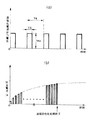
図16に、表示装置に用いた素子の、(放出電流Ie )対(素子印加電圧Vf)特性、および(素子電流If )対(素子印加電圧Vf )特性の典型的な例を示す。なお、放出電流Ie は素子電流If に比べて著しく小さく、同一尺度で図示するのが困難であるうえ、これらの特性は素子の大きさや形状等の設計パラメータを変更することにより変化するものであるため、2本のグラフは各々任意単位で図示した。
【0132】
表示装置に用いた素子は、放出電流Ie に関して以下に述べる3つの特性を有している。
【0133】
第一に、ある電圧(これを閾値電圧Vthと呼ぶ)以上の大きさの電圧を素子に印加すると急激に放出電流Ie が増加するが、一方、閾値電圧Vth未満の電圧では放出電流Ie はほとんど検出されない。すなわち、放出電流Ie に関して、明確な閾値電圧Vthを持った非線形素子である。
【0134】
第二に、放出電流Ie は素子に印加する電圧Vf に依存して変化するため、電圧Vf で放出電流Ie の大きさを制御できる。
【0135】
第三に、素子に印加する電圧Vf に対して素子から放出される電流Ie の応答速度が速いため、電圧Vf を印加する時間の長さによって素子から放出される電子の電荷量を制御できる。
【0136】
以上のような特性を有するため、表面伝導型放出素子を表示装置に好適に用いることができた。たとえば多数の素子を表示画面の画素に対応して設けた表示装置において、第一の特性を利用すれば、表示画面を順次走査して表示を行うことが可能である。すなわち、駆動中の素子には所望の発光輝度に応じて閾値電圧Vth以上の電圧を適宜印加し、非選択状態の素子には閾値電圧Vth未満の電圧を印加する。駆動する素子を順次切り替えてゆくことにより、表示画面を順次走査して表示を行うことが可能である。
【0137】
また、第二の特性か、または第三の特性を利用することにより、発光輝度を制御することができるため、階調表示を行うことが可能である。
【0138】
上述した実施形態による電子放出素子、電子ビーム源、表示パネルによって、平板型画像形成装置を製造し、不図示の表示ドライブ回路を設けて、例えばX方向配線に画像信号を、Y方向配線に走査信号を印加し、メタルバックに直流高電圧3kV以上を印加して駆動することにより、フェースプレート側から観察すると、高画質、高品質の画像を表出することができる。
【0139】
【実施例】
以下本発明の具体的な実施例について図面を用いて説明する。
【0140】
(実施例1)
本実施例では、まず未フォーミングの複数の表面伝導型電子源14を基板13に形成した。基板13として表面を清浄化した青板ガラスを用い、これに、図9に示した表面伝導型電子放出素子を160個×720個マトリクス状に形成した。
【0141】
素子電極24、25はPtスパッタ膜であり、X方向配線15、Y方向配線16はスクリーン印刷法により形成したAg配線である。導電性薄膜26はPdアミン錯体溶液を焼成したPdO微粒子膜である。
【0142】
画像形成部材であるところの蛍光膜20は図10(a)に示すように、各色蛍光体がY方向に伸びるストライプ形状を採用し、黒色体20aとしては各色蛍光体間だけでなく、X方向にも設けることでY方向の画素間を分離しかつスペーサ22を設置するための部分を加えた形状を用いた。先に黒色体(導電体)20aを形成し、その間隙部に各色蛍光体を塗布して蛍光膜20を作成した。ブラックストライプ(黒色体20a)の材料として通常良く用いられている黒鉛を主成分とする材料を用いた。フェースプレート19に蛍光体を塗布する方法はスラリー法を用いた。
【0143】
また、蛍光膜20より内面側(電子源側)に設けられるメタルバック21は、蛍光膜20の作成後、蛍光膜20の内面側表面の平滑化処理(通常フィルミングと呼ばれる)を行い、その後、Alを真空蒸着することで作成した。フェースプレート19には、更に蛍光膜20の導電性を高めるため、蛍光膜20より外面側(ガラス基板と蛍光膜の間)に透明電極が設けられる場合もあるが、本実施例ではメタルバックのみで十分な導電性が得られたので省略した。
【0144】
図7において、スペーサ22は清浄化したソーダライムガラスからなる絶縁性基材24(高さ3.8mm、板厚200μm、長さ20mm)上に、Cr2 O3 膜の第一層23aを真空成膜法により形成し成膜した。本実施例で用いたCr2 O3 はスパッタリング装置を用いてアルゴンと酸素の混合雰囲気中でCr2 O3 のターゲットをスパッタすることにより成膜した。
【0145】
成膜室にアルゴンを0.7Pa 、酸素を0.3Pa 導入し、酸化クロムのターゲットには8.3W/cm2 を印加した。45分間成膜を行なうことにより200nmの酸化クロム膜を得た。
【0146】
これらの試料を第一層23aとして成膜後、第二層23bのCr−Al2 O3 サーメット膜を成膜した。本実施例で用いたCr−Al2 O3 サーメット膜はスパッタリング装置を用いてアルゴン雰囲気中でCrとAl2 O3 のターゲットを同時にスパッタすることにより成膜した。
【0147】
成膜室にアルゴンを0.7Pa 導入し、それぞれのターゲットにかける電力を変化することにより組成の調節を行ない、抵抗値の調節を行なった。膜厚は2μmとした。
【0148】
このようにして作成したスペーサ表面に凹凸をつけるために、網目状のマスクをスペーサにかぶせ、アルゴン雰囲気下スパッタすることによりCr−Al2 O3 サーメット膜を物理エッチングした。スパッタの条件はAr分圧が1.0Pa、投入電力が2.0W/cm2 であり、30分間スパッタすることにより約200nmのCr−Al2 O3 サーメット膜をエッチングすることができる。本実施例では300分の物理スパッタを行ない、図Aに示すような表面構造のスペーサを得ることができた。
【0149】
このスペーサ22に関して、500℃、1時間の熱処理をすることによりスペーサ22の作成を終了した。この試料の成膜条件を次に示す。
【0150】

【0151】
その後、電子源14の3.8mm上方にフェースプレート19を支持枠18を介して配置し、リアプレート13、フェースプレート19、支持枠18およびスペーサ22の接合部を固定した。スペーサはX方向配線15上に等間隔に固定した。スペーサ22はフェースプレート19側では黒色体20a(線幅300μm)上に、Auを被覆シリカ球を含有した導電性フリットガラス26を用いることにより、帯電防止膜23とフェースプレート19との導通を確保した。なお、メタルバック21とスペーサ22とが当接する領域においてはメタルバック21の一部を除去した。リアプレート17と支持枠18の接合部はフリットガラス(不図示)を塗布し、大気中で420℃で10分以上焼成することで封着した。
【0152】
以上のようにして完成したあと、排気管を通じ真空ポンプにて排気し、十分低い圧力に達した後、容器外端子Dx1〜DxmとDy1〜Dynを通じ電子放出素子14の素子電極27、28間に電圧を印加し、導電性薄膜29を通電処理(フォーミング処理)することにより電子放出部30を形成した。フォーミング処理は、図12に示した波形の電圧を印加することにより行った。
【0153】
次に排気管を通してアセトンを0.133Pa の圧力となるように真空容器に導入し、容器外端子Dx1〜Dxmと、Dy1〜Dynに電圧パルスを定期的に印加することにより、炭素あるいは炭素化合物を堆積する通電活性化処理を行った。通電活性化は図13(a)に示すような波形を印加することにより行った。
【0154】
次に容器全体を200℃に加熱しつつ10時間真空排気した後、10-4Pa 程度の圧力で、排気管をガスバーナーで熱することで溶着し封止を行った。最後に、封止後の圧力を維持するために、ゲッター処理を行った。
【0155】
以上のように完成した画像形成装置において、各電子放出素子14には、容器外端子Dx1〜Dxm、Dy1〜Dynを通じ走査信号及び変調信号を不図示の信号発生手段よりそれぞれ印加することにより電子を放出させ、メタルバック21には、高圧端子Hv を通じて高圧を印加することにより放出電子ビームを加速し、蛍光膜20に電子を衝突させ、蛍光体20bを励起・発光させることで画像を表示した。なお高圧端子Hv への印加電圧Va は1〜5kV、素子電極27、28間への印加電圧Vf は14Vとした。この時、スペーサの試料Aに関しては上記駆動条件においてのスペーサ近傍のビームずれはないか、あっても非常に少なく、テレビ画像として問題のない範囲であった。
【0156】
また、第二層23bは、Cr−Al2 O3 サーメット膜の抵抗温度係数は−0.3%/℃から−0.33%/℃であり、上記駆動条件において熱暴走することはなかった。
【0157】
(参考例)
参考例においては第一層23aを酸化ニオブNb2O5とした。スパッタによる成膜を行い、成膜条件については以下の通りである。まず、スパッタリングターゲットとしてはNb2O5の焼結体を用いた。成膜室にArを0.4Pa、O2を0.1Pa の分圧で導入し、ターゲットには3.8W/cm2の電力を投入した。50分間成膜を行なうことにより100nmの膜厚のNb2O5膜を得た。この膜の比抵抗を測定した所、通常の抵抗測定装置では測定不可能な領域であり、比抵抗は108Ωcm以上であることが示された。
【0158】
次に第二層23bとしてPtを用いた島状膜を形成した。スパッタガスはアルゴンで全圧は1Pa である。1.0W/cm2 の投入電力でPtターゲットをスパッタすることによりPtの島状膜を得た。この膜をSEM観察したのが、図18に示す平面図と断面図である。このようにして作成したスペーサの抵抗値は1.1×10⁵ Ωcmであった。
【0159】
この後の組立工程は実施例1と同様に行ない、実施例1と同様の条件で駆動した。本参考例においてはこの駆動条件においてスペーサ近傍のビームずれはないか、あっても非常に少なく、テレビ画像として問題のない範囲であった。
【0160】
また、全組立工程を経過し、画像を表示した後の装置を分解して本参考例に用いたスペーサの抵抗を測定した所、比抵抗が7.6×10⁵Ωcmになっていた。
【0161】
(実施例2)
実施例2においては第一層23aの材料をY2O3とした。イオンビームスパッタによる成膜を行い、成膜条件については以下の通りである。まず、スパッタリングターゲットとしてはY2O3の焼結体を用いた。成膜室にAr0.4Pa、O20.1Pa 導入した。ターゲットに8.3W/cm2を印加した。40分間成膜を行なうことにより200nmの酸化イットリウム膜を得た。
【0162】
次に第二層23bとして酸化インジウムを用いた。これについては酸化インジウムの前駆体物質をディッピングによりコートし、焼成することで作成を行なった。条件及び出来上がりの試料については以下の通りである。
【0163】
【0164】
その後の組立工程は実施例1と同様に行ない、実施例1と同様の条件で駆動した。本実施例においてはこの駆動条件においてスペーサ近傍のビームずれはないか、あっても非常に少なく、テレビ画像として問題のない範囲であった。
【0165】
【発明の効果】
以上説明した通り、二次電子放出効率の小さい材料による膜の上に、導電性を有する膜を、ネットワーク構造、島状またはそれらの混在する構造とすることで、第一層、第二層のどちらに電子が入射しても、帯電を抑える効果がある。また、第二層が導電性を有することで、除電効果も得られた。また、これを使用した画像形成装置はスペーサ近傍でのビーム電位の乱れは抑止され、ビームが蛍光体に衝突する位置と、本来発光するべき蛍光体との位置ずれのない鮮明な画像表示が可能である。
【図面の簡単な説明】
【図1】本発明の実施例である画像表示装置の、表示パネルの一部を切り欠いて示した斜視図である。
【図2】本発明による画像表示装置のスペーサ周辺の断面図である。
【図3】本発明の実施例で用いた第二層がネットワーク構造と島状の混合状態の構造であるスペーサ表面の拡大図である。
【図4】本発明の実施例で用いた第二層がネットワーク構造であるスペーサ表面の拡大図である。
【図5】 本発明の参考例で用いた第二層が島状であるスペーサ表面の拡大図である。
【図6】 本発明の実施例で用いた第二層がネットワーク構造であるスペーサ表面の拡大図である。
【図7】本発明で用いたスペーサの断面模式図である。
【図8】本実施例で用いたマルチ電子ビーム源の基板の平面図である。
【図9】実施例で用いた平面型の表面伝導型放出素子の平面図(a),断面図(b)である。
【図10】表示パネルのフェースプレートの蛍光体配列を例示した平面図である。
【図11】平面型の表面伝導型放出素子の製造工程を示す断面図である。
【図12】通電フォーミング処理の際の印加電圧波形である。
【図13】通電活性化処理の際の印加電圧波形(a)、放出電流Ie の変化(b)である。
【図14】実施例で用いた垂直型の表面伝導型放出素子の断面図である。
【図15】垂直型の表面伝導型放出素子の製造工程を示す断面図である。
【図16】実施例で用いた表面伝導型放出素子の典型的な特性を示すグラフである。
【図17】本発明の第1の実施例で用いたスペーサ表面の拡大図と断面図である。
【図18】 本発明の参考例で用いたスペーサ表面の拡大図と断面図である。
【図19】 本発明の第2の実施例で用いたスペーサ表面の拡大図と断面図である。
【図20】従来知られた表面伝導型放出素子の一例の構造図である。
【図21】従来知られたFE型素子の一例の構造図である。
【図22】従来知られたMIM型素子の一例の構造図である。
【符号の説明】
1 基板
2 導電性薄膜
3 電子放出部
4 基板
5 エミッタ配線
6 エミッタコーン
7 絶縁層
8 ゲート電極
9 基板
10 下電極
11 絶縁層
12 上電極
13 基板
14 冷陰極素子
15 行方向配線
16 列方向配線
17 リアプレート
18 側壁
19 フェースプレート
20 蛍光膜
21 メタルバック
22 スペーサ
23 導電膜
23a 第一層(下引き層)
23b 第二層(キャップ層)
24 絶縁性基材
25 中間層電極
26 導電性フリット(当接材)
27,28 素子電極
29 導電性薄膜
30 電子放出部
31 通電活性化処理により形成した薄膜
32 フォーミング用電源
33 電流計
34 活性化用電源
35 アノード電極
36 直流高電圧電源
37 電流計
38 基板
39 素子電極
40 素子電極
41 導電性薄膜
42 電子放出部
43 段差形成部材
44 通電活性化により形成した薄膜
57 基板上の絶縁層[0001]
BACKGROUND OF THE INVENTION
The present invention relates to an image forming apparatus, and is particularly suitable for a flat image forming apparatus in which a plurality of electron-emitting devices are arranged.
[0002]
[Prior art]
Conventionally, two types of electron-emitting devices, a hot cathode device and a cold cathode device, are known. Among these, in the cold cathode device, for example, a surface conduction electron-emitting device, a field emission electron-emitting device (hereinafter referred to as FE type), a metal / insulating layer / metal-type electron emitting device (hereinafter referred to as MIM type), etc. It has been known.
[0003]
The surface conduction electron-emitting device utilizes a phenomenon in which electron emission occurs when a current flows in parallel to a film surface of a small-area thin film formed on a substrate. As this surface conduction electron-emitting device, SnOl by Erinson et al.2Thin film [M.I.Elinson, Radio Eng. Electron Phys., 10, 1290, (1965)], Au thin film [G.D Mitter: “Thin Solid Films”, 9,317 (1972)], In2OThree/ SnO2Thin film [M. Hartwell And CGFonstad: "IEEE Trans.ED Conf.", 519 (1975)], carbon thin film [Haraki Araki et al .: Vacuum, Vol. 26, No. 1, 22 (1983) ] Have been reported.
[0004]
As a typical example of the device configuration of these surface conduction electron-emitting devices, FIG. 20 shows a plan view of the device by M. Hartwell et al. In the figure, 1 is a substrate, and 2 is a conductive thin film made of a metal oxide formed by sputtering. The conductive
[0005]
In the energization forming, the conductive
[0006]
Examples of the FE type include, for example, WPDyke & W.W.Dolan, “Field Emission”, Advance in Electron Physics, 8, 89 (1956), or CASpindt, “Physical Properties of Thin-Film Field Emission cathodes with molybdenium. Cones ", J. Appl. Phys., 47, 5248 (1976).
[0007]
As a typical example of the FE type device configuration, FIG. 21 shows a cross-sectional view of the device according to C.A. In the figure, 4 is a substrate, 5 is an emitter wiring made of a conductive material, 6 is an emitter cone, 7 is an insulating layer, and 8 is a gate electrode. This element causes field emission from the tip of the
[0008]
As another element configuration of the FE type, there is an example in which an emitter and a gate electrode are arranged on a substrate substantially parallel to the substrate plane, in addition to the laminated structure as shown in FIG.
[0009]
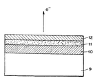
As an example of the MIM type, for example, CAMead, “Operation of Tunnel-Emission Devices, J. Appl. Phys., 32, 646 (1961), etc. is known. 22 is a cross-sectional view, in which 9 is a substrate, 10 is a lower electrode made of metal, 11 is a thin insulating layer having a thickness of about 100 angstroms, and 12 is about 80 to 300 angstroms in thickness. In the MIM type, electrons are emitted from the surface of the
[0010]
The various cold cathode devices described above do not require a heater because they can obtain electron emission at a lower temperature than the hot cathode devices. Therefore, the structure is simpler than that of the hot cathode device, and a fine device can be produced. Further, even if a large number of elements are arranged on the substrate at a high density, problems such as thermal melting of the substrate hardly occur. Further, unlike the case where the hot cathode element operates by heating of the heater, the response speed is slow. In the case of the cold cathode element, there is also an advantage that the response speed is fast.
[0011]
Examples of the application of the cold cathode device described above include image forming apparatuses such as image display apparatuses and image recording apparatuses, and charged beam sources.
[0012]
In particular, as an example of applying a cold cathode device to an image display device, USP by the present applicant.
As disclosed in US Pat. No. 5,066,833, Japanese Patent Laid-Open No. 2-257551, and Japanese Patent Laid-Open No. 4-28137, a surface conduction electron-emitting device and a phosphor that emits light when irradiated with an electron beam are used in combination. Image display devices have been studied. There is an image display device that emits light using a combination of a surface conduction electron-emitting device and a phosphor that emits light when irradiated with an electron beam by the surface conduction electron-emitting device.
[0013]
Also, as an example of applying a large number of FE types to an image display device, a flat panel display device reported by R. Meyer et al. Is known [R. Meyer: “Recent Development on Microchips Display at LETI”, Tech. Digest of 4th Int. Vacuum Micro Electronics Conf., Nagahama, pp. 6-9 (1991)].
[0014]
An example in which a large number of MIM types are arranged and applied to an image display device is disclosed in Japanese Patent Laid-Open No. 3-55738 by the present applicant.
[0015]
Among each cold cathode type, the surface conduction electron-emitting device has an advantage that it is easy to form a large number of devices in a large area because of its simple structure and easy manufacture.
[0016]
Compared with liquid crystal display devices, image display devices using a combination of surface-conduction electron-emitting devices and phosphors are self-luminous and do not require a backlight or have a wide viewing angle. Yes.
[0017]
In the flat type image display device, a large number of the above-described electron-emitting devices are arranged on a flat substrate, and a phosphor that emits light by electrons is arranged opposite to the flat substrate. The electron-emitting devices are arranged on the substrate in a two-dimensional matrix (referred to as a multi-electron source), and each device is connected to the row direction wiring and the column direction wiring. As an example of the image display method, there is the following simple matrix drive.
[0018]
In order to emit electrons from any one row in the matrix, a selection voltage is applied in the row direction, and a signal voltage is applied to the column wiring in synchronization therewith.
[0019]
Electrons emitted from the electron-emitting devices in the selected row are accelerated toward the phosphor to excite the phosphor and emit light. An image is displayed by sequentially applying a selection voltage in the row direction.
[0020]
It is necessary to maintain a vacuum between the substrate (rear plate) on which the electron-emitting devices are formed in a two-dimensional matrix and the substrate (face plate) on which the phosphor and the acceleration electrode are formed. Since atmospheric pressure is applied to the rear plate and the face plate, a substrate having a thickness that supports atmospheric pressure is required as the display device becomes larger. However, increasing the thickness of both substrates, such as glass, increases the weight. Inserting a support member (spacer) between the rear plate and the face plate can reduce the weight and increase the distance between the rear plate and the face plate. A structure is adopted that keeps constant and prevents damage to the rear plate and the face plate.
[0021]
The spacer is required to have pressure resistance to atmospheric pressure and sufficient mechanical strength to support it, and should not greatly affect the trajectory of electrons flying between the rear plate and the face plate. The cause of the influence on the electron trajectory is the charging of the spacer. In spacer charging, a part of the electrons emitted from the electron source or the electrons reflected by the face plate enter the spacer, and secondary ions are emitted from the spacer, or ions ionized by the collision of the electrons adhere to the surface. This is probably due to this.
[0022]
When the spacer is positively charged, electrons flying in the vicinity of the spacer are attracted to the spacer, so that the display image is distorted in the vicinity of the spacer. The effect of charging becomes more prominent as the distance between the rear plate and the face plate increases.
[0023]
In general, as a means for suppressing charging, conductivity is imparted to the charging surface and the electric charge is removed by passing a slight current. Japanese Unexamined Patent Publication No. 57-118355 discloses a method of applying this concept to a spacer and coating the surface of the spacer with tin oxide. Japanese Patent Laid-Open No. 3-49135 discloses a method of covering with a PdO-based glass material.
[0024]
In addition, high brightness as an image display device is an important factor. In order to efficiently emit the phosphor formed on the face plate, it is only necessary to irradiate the phosphor with electrons accelerated at a high voltage, and in order to emit light with sufficient efficiency, the electrons are preferably 3 kV or higher, preferably Accelerate to 5 kV or higher. Therefore, a voltage of several kV or more is applied between the rear plate and the face plate, and a voltage having substantially the same potential is applied to both ends of the spacer. The material used for the spacer is required not to discharge when an acceleration voltage is applied.
[0025]
As a means for improving the creeping discharge withstand voltage, it is effective to cover the surface with a material having a low secondary electron emission rate. Examples of coating with a material with a low secondary electron emission rate include chromium oxide (TSSudarshan and JDCross: IEEE Tran.EI-11, 32 (1976)), copper oxide (JDCross and TSsudarshan: IEEE Tran.EI- 9146 (1974)) is known.
[0026]
[Problems to be solved by the invention]
However, when the above oxide semiconductor material is applied to a spacer of an image display device having a multi-electron source, sufficient performance may not be exhibited in the following points. That is, since the oxide semiconductor material has a low specific resistance value, the current flowing through the spacer surface is too large unless it is coated very thinly. When the resistance value is low, in the image display device using a high acceleration voltage, heat generation of the spacer portion becomes a problem. In addition, the resistance value of oxide semiconductors varies greatly depending on the atmospheric gas, so the variation is large, and it is difficult to control resistance with a very thin thin film, and therefore, the spacer cannot be manufactured with good reproducibility.
[0027]
In other words, although the physical properties preferred as the material of the spacer or its surface layer have been predicted, it is represented by an image display device that accelerates the electrons emitted from the multi-electron source with a voltage of 3 kV or more, thereby causing the phosphor to emit light. There was no material suitable as a spacer for an image forming apparatus. Therefore, it has been difficult to realize an image forming apparatus that forms a high-brightness and distortion-free image by causing the phosphor to emit light with a high voltage.
[0028]
It is an object of the present invention to provide a structure and material of a spacer surface layer suitable for the image forming apparatus as a spacer, and to provide an image forming apparatus capable of displaying an image having high brightness and no distortion.
[0029]
[Means for Solving the Problems]
The image forming apparatus of the present invention includes:An electron source that emits electrons and the plate are opposed to each other through a spacer.In the image forming apparatus having the structure, the spacer isA substrate, a first layer made of an insulating film covering the surface of the substrate, and a second layer made of a semiconductive film covering the first layer, a part of the first layer being , Exposed in islands at multiple locations from the second layerAn image forming apparatus characterized by the above.
[0031]
DETAILED DESCRIPTION OF THE INVENTION
Embodiments according to the present invention will be described in detail with reference to the drawings.
[0032]
[Description of display panel]
FIG. 1 is a perspective view of a display panel as an application example of an image display device according to an embodiment of the present invention, and a part of the panel is cut away to show the internal structure. In the figure,
[0033]
Further, in FIG. 1, a
[0034]
[Composition and action of spacer]
Next, the configuration and operation of the spacer used in the display panel of the image display device to which the present invention is applied will be described with a specific example.
[0035]
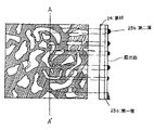
2 is a schematic cross-sectional view of the display device taken along line A-A ′ shown in FIG. Each number corresponds to FIG. In FIG. 2,
[0036]
The
[0037]
The insulating
[0038]
As a result of studying a method for preventing the
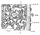
[0039]
Here, a schematic diagram of a network structure or an island-like structure as the
[0040]
FIG. 7 is a schematic diagram showing the structure of the spacer. On the insulating
[0041]
The first layer 23a is made of a material having a low secondary electron emission efficiency, and the
[0042]
The material of the exposed portion is an insulator although the secondary electron emission efficiency is low, and once charged, it is difficult to remove the charge only by the action of the first layer. Therefore, the charge is removed by letting the charged charges escape to the
[0043]
In addition, the resistance value of the
When the resistance temperature coefficient of the
[0044]
1 cm of the
[0045]
The thickness t of the first layer 23a is preferably 10 nm or more. On the other hand, when the film thickness t exceeds 1 μm, the film stress increases and the risk of film peeling increases, and the film formation time becomes longer, resulting in poor productivity. Therefore, the film thickness is desirably 10 nm to 1 μm, more preferably 20 nm to 500 nm.
[0046]
As the material of the
[0047]
The overall resistance value of the
[0048]
As the material used for the first layer 23a, a material having a low secondary electron emission rate is preferable. Cr2OThree, Nb2OFive, Y2OThreeIs a material suitable for use in the first layer 23a because of its low secondary electron emission efficiency. According to the authors' measurements, the secondary electron emission efficiency of these materials does not exceed 1.8 at the maximum at an incident angle of 0 °.
[0049]
However, the material of these first layers 23a is 10% in volume resistance.8Since it is an insulator having a resistance value of Ωcm or more and it is difficult to release charges, it cannot be used alone. However, by using it as the first layer 23a having the configuration of the two
[0050]
The first layer 23a is formed of an insulating
[0051]
The
[0052]
Next, the configuration and manufacturing method of the display panel of the image display device to which the present invention is applied will be described with reference to specific examples.
[0053]
[Display panel]
FIG. 1 is a perspective view of the display panel used in the present embodiment described above, and a part of the panel is cut away to show the internal structure.
[0054]
A
[0055]
As long as the multi-electron beam source used in the image display apparatus according to the present invention is an electron source in which the cold cathode elements are wired in a simple matrix, there is no limitation on the material, shape or manufacturing method of the cold cathode elements. Therefore, for example, a cold cathode device such as a surface conduction electron-emitting device, FE type, or MIM type can be used. It is also possible to form the electron source directly on the rear plate.
[0056]
Next, the structure of a multi-electron beam source in which surface conduction electron-emitting devices (to be described later) are arranged on a substrate as a cold cathode device and simple matrix wiring is described.
[0057]
FIG. 8 is a plan view of the multi-electron beam source used in the display panel of FIG. On the
[0058]
[Configuration and operation of multi-electron source]
FIG. 9A is a plan view taken along line BB ′ of FIG. 8, and FIG. 9B is a cross-sectional view thereof.
[0059]
Note that the multi-electron source having such a structure includes the row-
[0060]
In this embodiment, the multi-electron
[0061]
[Configuration and action of face plate]
A
[0062]
Further, the method of separately applying the phosphors of the three primary colors is not limited to the stripe arrangement shown in FIG. 10 (a). For example, a delta arrangement as shown in FIG. It may be an array.
[0063]
When producing a monochrome display panel, a monochromatic phosphor material may be used for the phosphor film 20b, and a black conductive material is not necessarily used.
[0064]
Further, a metal back 21 known in the field of CRT is provided on the surface of the
[0065]
[Operation and function of spacer]
As shown in FIG. 2, the
[0066]
The low-
[0067]
(1) The
[0068]
As already described, the
[0069]
(2) The potential distribution of the
[0070]
Electrons emitted from the
[0071]
(3) Control the orbit of emitted electrons.
[0072]
Electrons emitted from the
[0073]
For the
[0074]
The
[0075]
[Production and operation of display panel]
In addition, Dx1 to Dxm and Dy1 to Dyn and Hv shown in FIG. 1 are electrical connection terminals having an airtight structure provided to electrically connect the display panel and an electric circuit (not shown). Dx1 to Dxm are electrically connected to the
[0076]
In order to evacuate the inside of the hermetic container to a vacuum, after assembling the hermetic container, an exhaust pipe (not shown) and an exhaust pump are connected to evacuate the inside of the hermetic container.-FiveEvacuate to a degree of vacuum of Pa. Thereafter, the exhaust pipe is sealed. In order to maintain the degree of vacuum in the hermetic container, a getter film (not shown) is formed at a predetermined position in the hermetic container immediately before or after sealing. A getter film is a film formed by, for example, heating and vapor-depositing a getter material mainly composed of Ba by a heater or high-frequency heating, and the inside of an airtight container is 1 × 10 6 by the adsorption action of the getter film.-3Or 1 × 10-FiveThe vacuum degree of Pa is maintained.
[0077]
In the image display device using the display panel described above, electrons are emitted from each
[0078]
Usually, the applied voltage to the surface conduction electron-emitting
[0079]
The basic configuration and manufacturing method of the display panel according to the embodiment of the present invention and the outline of the image display device have been described above.
[0080]
[Configuration and Manufacturing Method of Multi Electron Beam Source]
Next, the manufacturing method of the multi electron beam source used for the display panel of the embodiment will be described. As long as the multi-electron beam source used in the image display apparatus related to the image display apparatus of the present invention is an electron source in which cold cathode elements are wired in a simple matrix, there is no limitation on the material, shape or manufacturing method of the cold cathode elements. Therefore, for example, a cold cathode device such as a surface conduction electron-emitting device, FE type, or MIM type can be used.
[0081]
However, a surface conduction electron-emitting device is particularly preferable among these cold cathode devices under the circumstances where a display device having a large display screen and a low price is required. That is, in the FE type, the relative position and shape of the emitter cone and the gate electrode greatly affect the electron emission characteristics, and thus an extremely accurate manufacturing technique is required. This achieves a large area and a reduction in manufacturing cost. This is a disadvantageous factor. Further, in the MIM type, it is necessary to make the insulating layer and the upper electrode thin and uniform, but this is also a disadvantageous factor in achieving an increase in area and a reduction in manufacturing cost.
[0082]
In that respect, since the surface conduction electron-emitting device is relatively simple to manufacture, it is easy to increase the area and reduce the manufacturing cost. Further, the inventors have found that among the surface conduction electron-emitting devices, those in which the electron emission portion or its peripheral portion is formed of a fine particle film are particularly excellent in electron emission characteristics and can be easily manufactured. Therefore, it can be said that it is most suitable for use in a multi-electron beam source of a high-luminance and large-screen image display device. Therefore, in the display panel of the above embodiment, a surface conduction electron-emitting device in which the electron emission portion or its peripheral portion is formed of a fine particle film is used. First, the basic configuration, manufacturing method and characteristics of a suitable surface conduction electron-emitting device will be described, and then the structure of a multi-electron beam source in which a number of devices are wired in a simple matrix will be described.
[0083]
(Suitable device configuration and manufacturing method for surface conduction electron-emitting devices)
There are two types of typical structures of the surface conduction electron-emitting device in which the electron emission portion or the peripheral portion thereof is formed of a fine particle film, a planar type and a vertical type.
[0084]
(Plane type surface conduction electron-emitting device)
First, the device configuration and manufacturing method of a planar surface conduction electron-emitting device will be described. FIG. 9 shows a plan view (a) and a cross-sectional view (b) for explaining the configuration of a planar surface conduction electron-emitting device. In the figure, 13 is a substrate, 27 and 28 are element electrodes, 29 is a conductive thin film, 30 is an electron emission portion formed by energization forming treatment, and 31 is a thin film formed by energization activation treatment.
[0085]
As the
[0086]
The
[0087]
The shapes of the
[0088]
A fine particle film is used for the conductive
[0089]
The particle diameter of the fine particles used for the fine particle film is in the range of several angstroms to several thousand angstroms, and the preferred one is in the range of 10 angstroms to 200 angstroms. The film thickness of the fine particle film is appropriately set in consideration of various conditions as described below. That is, the conditions necessary for electrically connecting to the
[0090]
Examples of materials that can be used to form the fine particle film include Pd, Pt, Ru, Ag, Au, Ti, In, Cu, Cr, Fe, Zn, Sn, Ta, W, and Pb. Metals such as PdO, SnO2, In2OThree, PbO, Sb2OThreeOxides such as HfB2, ZrB2, LaB6, CeB6, YBFour, GdBFour, Borides such as TiC, ZrC, HfC, TaC, SiC, WC, etc., nitrides including TiN, ZrN, HfN, etc., Si, Ge, etc. And the like, carbon, and the like, which are appropriately selected from these.
[0091]
As described above, the conductive
[0092]
Note that the conductive
[0093]
Moreover, the
[0094]
The
[0095]
The
[0096]
The basic configuration of a preferable element has been described above. In the embodiment, the following element is used.
[0097]
That is, blue glass was used for the
[0098]
Pd or PdO was used as the main material of the fine particle film, the thickness of the fine particle film was about 100 [angstrom], and the width W was 100 [micrometer].
[0099]
(Planar surface conduction electron-emitting device manufacturing method)
Next, a preferred method for manufacturing a planar surface conduction electron-emitting device will be described.
[0100]
FIGS. 11A to 11D are cross-sectional views for explaining the manufacturing process of the surface conduction electron-emitting device, and the notations of the respective members are the same as those in FIG.
[0101]
(1) First,
[0102]
In the formation, the
[0103]
(2) Next, a conductive
[0104]
In forming the film, first, an organic metal solution is applied to the substrate (a), dried, heated and fired to form a fine particle film, and then patterned into a predetermined shape by photolithography and etching. Here, the organometallic solution is a solution of an organometallic compound whose main element is a fine particle material used for the conductive
[0105]
Further, as a method for forming the conductive
[0106]
(3) Next, as shown in FIG. 11C, an appropriate voltage is applied between the forming power source 32 between the
[0107]
The energization forming process is a process in which a conductive
[0108]
In order to explain the energization method in more detail, FIG. 12 shows an example of an appropriate voltage waveform applied from the forming power supply 32. When forming a conductive thin film made of a fine particle film, a pulsed voltage is preferable. In this embodiment, a triangular wave pulse having a pulse width T1 is continuously applied at a pulse interval T2 as shown in FIG. Applied. At that time, the peak value Vpf of the triangular wave pulse was boosted sequentially. Further, a monitor pulse Pm for monitoring the formation state of the
[0109]
In the present embodiment, for example, 10-3In a vacuum atmosphere of about Torr, for example, the pulse width T1 was set to 1 [millisecond], the pulse interval T2 was set to 10 [millisecond], and the peak value Vpf was increased by 0.1 [V] for each pulse. The monitor pulse Pm was inserted at a rate of once every
[0110]
The above method is a preferable method for the surface conduction electron-emitting device of the present embodiment. For example, when the design of the surface conduction electron-emitting device such as the material and film thickness of the fine particle film or the element electrode interval L is changed. Accordingly, it is desirable to change the energization conditions accordingly.
[0111]
(4) Next, as shown in FIG. 11 (d), an appropriate voltage is applied between the
[0112]
The energization activation process is a process of energizing the
[0113]
Specifically, 10-110-FourBy applying a voltage pulse periodically in a vacuum atmosphere within the range of Pa, carbon or a carbon compound originating from an organic compound present in the vacuum atmosphere is deposited. The
[0114]
In order to explain the energization method in more detail, FIG. 13A shows an example of an appropriate voltage waveform applied from the
[0115]
[0116]
The energization conditions described above are preferable conditions for the surface conduction electron-emitting device of the present embodiment, and when the design of the surface conduction electron-emitting device is changed, it is desirable to change the conditions accordingly.
[0117]
As described above, the planar surface conduction electron-emitting device shown in FIG. 9B was manufactured.
[0118]
(Vertical surface conduction electron-emitting devices)
Next, another representative configuration of the surface conduction electron-emitting device in which the electron emission portion or its periphery is formed of a fine particle film, that is, the configuration of a vertical surface conduction electron-emitting device will be described.
[0119]
FIG. 14 is a schematic cross-sectional view for explaining a vertical basic configuration, in which 38 is a substrate, 39 and 40 are element electrodes, 43 is a step forming member, and 41 is a conductive film using a fine particle film. , 42 is an electron emission portion formed by energization forming treatment, and 44 is a thin film formed by energization activation treatment.
[0120]
The vertical type is different from the planar type described above in that one
[0121]
Next, a method for manufacturing a vertical surface conduction electron-emitting device will be described. (A)-(e) of FIG. 15 is sectional drawing for demonstrating a manufacturing process, and the description of each member is the same as the said FIG.
[0122]
(1) First, as shown in FIG. 15A, the
[0123]
(2) Next, as shown in FIG. 2B, an insulating layer for forming a step forming member is laminated. For example, the insulating layer is made of SiO.2May be laminated by sputtering, but other film forming methods such as vacuum deposition and printing may be used.
[0124]
(3) Next, as shown in FIG. 3C, the
[0125]
(4) Next, as shown in FIG. 15D, a part of the insulating layer is removed by using, for example, an etching method to expose the
[0126]
(5) Next, as shown in FIG. 5E, a conductive
[0127]
(6) Next, as in the case of the planar type, an energization forming process is performed to form an electron emission portion. The energization forming process may be the same as the planar energization forming process described with reference to FIG.
[0128]
(7) Next, as in the case of the planar type, an energization activation process is performed to deposit carbon or a carbon compound in the vicinity of the electron emission portion. The energization activation process may be performed in the same manner as the planar energization activation process described with reference to FIG.
[0129]
As described above, the vertical surface conduction electron-emitting device shown in FIG. 14 was manufactured.
[0130]
(Characteristics of surface conduction electron-emitting devices used in display devices)
The device structure and manufacturing method of the planar and vertical surface conduction electron-emitting devices have been described above. Next, the characteristics of the devices used in the display device will be described.
[0131]
FIG. 16 shows typical examples of (emission current Ie) vs. (element applied voltage Vf) characteristics and (element current If) vs. (element applied voltage Vf) characteristics of the elements used in the display device. The emission current Ie is remarkably smaller than the device current If and is difficult to show on the same scale. Further, these characteristics are changed by changing design parameters such as the size and shape of the device. Therefore, the two graphs are shown in arbitrary units.
[0132]
The element used in the display device has the following three characteristics with respect to the emission current Ie.
[0133]
First, when a voltage larger than a certain voltage (referred to as a threshold voltage Vth) is applied to the device, the emission current Ie increases rapidly. On the other hand, at a voltage lower than the threshold voltage Vth, the emission current Ie is almost none. Not detected. That is, it is a non-linear element having a clear threshold voltage Vth with respect to the emission current Ie.
[0134]
Second, since the emission current Ie changes depending on the voltage Vf applied to the device, the magnitude of the emission current Ie can be controlled by the voltage Vf.
[0135]
Third, since the response speed of the current Ie emitted from the device is fast with respect to the voltage Vf applied to the device, the amount of electrons emitted from the device can be controlled by the length of time for which the voltage Vf is applied.
[0136]
Due to the above characteristics, the surface conduction electron-emitting device can be suitably used for a display device. For example, in a display device in which a large number of elements are provided corresponding to the pixels of the display screen, display can be performed by sequentially scanning the display screen by using the first characteristic. That is, a voltage equal to or higher than the threshold voltage Vth is appropriately applied to the driven element in accordance with the desired light emission luminance, and a voltage lower than the threshold voltage Vth is applied to the non-selected state element. By sequentially switching the elements to be driven, it is possible to display by sequentially scanning the display screen.
[0137]
Further, by using the second characteristic or the third characteristic, the light emission luminance can be controlled, so that gradation display can be performed.
[0138]
A flat panel image forming apparatus is manufactured by the electron-emitting device, the electron beam source, and the display panel according to the above-described embodiment, and a display drive circuit (not shown) is provided. By applying a signal and driving the metal back by applying a DC high voltage of 3 kV or higher, an image with high image quality and high quality can be displayed when viewed from the face plate side.
[0139]
【Example】
Hereinafter, specific embodiments of the present invention will be described with reference to the drawings.
[0140]
(Example 1)
In this example, a plurality of unformed surface-
[0141]
The
[0142]
As shown in FIG. 10A, the
[0143]
Further, the metal back 21 provided on the inner surface side (electron source side) than the
[0144]
In FIG. 7, a
[0145]
Argon was introduced into the film forming chamber by 0.7 Pa and oxygen was introduced by 0.3 Pa, and the chromium oxide target was 8.3 W / cm.2Was applied. The film was formed for 45 minutes to obtain a 200 nm chromium oxide film.
[0146]
After forming these samples as the first layer 23a, the Cr-Al of the
[0147]
Argon was introduced into the film forming chamber at 0.7 Pa, and the composition was adjusted by changing the power applied to each target, and the resistance value was adjusted. The film thickness was 2 μm.
[0148]
In order to make unevenness on the surface of the spacer thus prepared, a mesh mask is placed on the spacer and sputtered in an argon atmosphere to form Cr—Al2OThreeThe cermet film was physically etched. The sputtering conditions were Ar partial pressure of 1.0 Pa and input power of 2.0 W / cm.2About 200 nm of Cr—Al by sputtering for 30 minutes2OThreeThe cermet film can be etched. In this embodiment, physical sputtering was performed for 300 minutes, and a spacer having a surface structure as shown in FIG. A could be obtained.
[0149]
With respect to this
[0150]
[0151]
After that, the
[0152]
After completion as described above, after evacuating with a vacuum pump through an exhaust pipe and reaching a sufficiently low pressure, between the
[0153]
Next, acetone is introduced into the vacuum vessel through the exhaust pipe so as to have a pressure of 0.133 Pa, and a voltage pulse is periodically applied to the external terminals Dx1 to Dxm and Dy1 to Dyn. The energization activation process to deposit was performed. The energization activation was performed by applying a waveform as shown in FIG.
[0154]
Next, the whole container was evacuated for 10 hours while being heated to 200 ° C.-FourSealing was performed by welding the exhaust pipe with a gas burner at a pressure of about Pa. Finally, a getter process was performed to maintain the pressure after sealing.
[0155]
In the image forming apparatus completed as described above, electrons are applied to each electron-emitting
[0156]
The
[0157]
(referenceExample)
referenceIn the example, the first layer 23a is made of niobium oxide Nb.2OFiveIt was. Film formation by sputtering is performed, and the film formation conditions are as follows. First, as a sputtering target, Nb2OFiveThe sintered body was used. In the film formation chamber, Ar is 0.4 Pa, O2Is introduced at a partial pressure of 0.1 Pa, and the target is 3.8 W / cm.2The power was turned on. Nb with a film thickness of 100 nm is formed by performing film formation for 50 minutes.2OFiveA membrane was obtained. When the specific resistance of this film was measured, it was an area that could not be measured with a normal resistance measuring device.8It was shown to be Ωcm or more.
[0158]
Next, an island-shaped film using Pt was formed as the
[0159]
The subsequent assembly process was performed in the same manner as in Example 1 and was driven under the same conditions as in Example 1. BookreferenceIn the example, there was no beam deviation near the spacers under these driving conditions, or even very little, and there was no problem as a television image.
[0160]
Also, after the entire assembly process has passed, the device after displaying the image is disassembled and thereferenceWhen the resistance of the spacer used in the example was measured, the specific resistance was 7.6 × 10⁵It was Ωcm.
[0161]
(Example2)
Example2The material of the first layer 23a is Y2OThreeIt was. Film formation is performed by ion beam sputtering, and the film formation conditions are as follows. First, as a sputtering target, Y2OThreeThe sintered body was used. Ar0.4Pa, O in the deposition chamber20.1 Pa was introduced. 8.3 W / cm on the target2Was applied. A film was formed for 40 minutes to obtain a 200 nm yttrium oxide film.
[0162]
Next, indium oxide was used as the
[0163]
[0164]
Subsequent assembly steps were performed in the same manner as in Example 1 and were driven under the same conditions as in Example 1. In this embodiment, there was no beam deviation near the spacer under these driving conditions, or even very little, and there was no problem as a television image.
[0165]
【The invention's effect】
As described above, by forming a conductive film on a film made of a material having a low secondary electron emission efficiency into a network structure, an island shape, or a mixed structure thereof, the first layer and the second layer Regardless of which electron enters, there is an effect of suppressing charging. Moreover, the static elimination effect was acquired because the 2nd layer has electroconductivity. In addition, the image forming apparatus using this suppresses disturbance of the beam potential in the vicinity of the spacer, and can display a clear image with no positional deviation between the position where the beam collides with the phosphor and the phosphor that should emit light originally. It is.
[Brief description of the drawings]
FIG. 1 is a perspective view of an image display apparatus according to an embodiment of the present invention, with a part of a display panel cut away.
FIG. 2 is a cross-sectional view of the periphery of the spacer of the image display device according to the present invention.
FIG. 3 is an enlarged view of the spacer surface in which the second layer used in the embodiment of the present invention has a network structure and an island-like mixed structure.
FIG. 4 is an enlarged view of a spacer surface in which the second layer used in the embodiment of the present invention has a network structure.
FIG. 5 shows the present invention.referenceIt is an enlarged view of the spacer surface whose 2nd layer used in the example is island shape.
FIG. 6 is an enlarged view of a spacer surface in which the second layer used in the embodiment of the present invention has a network structure..
FIG. 7 is a schematic cross-sectional view of a spacer used in the present invention.
FIG. 8 is a plan view of a substrate of a multi-electron beam source used in this example.
FIGS. 9A and 9B are a plan view and a cross-sectional view of a planar surface conduction electron-emitting device used in Examples.
FIG. 10 is a plan view illustrating the phosphor array of the face plate of the display panel.
FIG. 11 is a cross-sectional view showing a manufacturing process of a planar surface conduction electron-emitting device.
FIG. 12 is an applied voltage waveform at the time of energization forming processing.
FIG. 13 shows an applied voltage waveform (a) and a change (b) in emission current Ie during energization activation processing.
FIG. 14 is a cross-sectional view of a vertical surface conduction electron-emitting device used in Examples.
FIG. 15 is a cross-sectional view showing a process for manufacturing a vertical surface conduction electron-emitting device.
FIG. 16 is a graph showing typical characteristics of the surface conduction electron-emitting device used in Examples.
FIGS. 17A and 17B are an enlarged view and a sectional view of a spacer surface used in the first embodiment of the present invention. FIGS.
FIG. 18 shows the present invention.Reference exampleIt is the enlarged view and sectional drawing of the spacer surface which were used in.
FIG. 19 shows the first of the present invention.2It is the enlarged view and sectional drawing of the spacer surface which were used in the Example.
FIG. 20 is a structural diagram of an example of a conventionally known surface conduction electron-emitting device.
FIG. 21 is a structural diagram of an example of a conventionally known FE type element.
FIG. 22 is a structural diagram of an example of a conventionally known MIM type element.
[Explanation of symbols]
1 Substrate
2 Conductive thin film
3 Electron emission part
4 Substrate
5 Emitter wiring
6 Emitter cone
7 Insulation layer
8 Gate electrode
9 Board
10 Lower electrode
11 Insulating layer
12 Upper electrode
13 Substrate
14 Cold cathode elements
15 Row direction wiring
16 column direction wiring
17 Rear plate
18 Side wall
19 Face plate
20 Fluorescent film
21 Metal back
22 Spacer
23 Conductive film
23a First layer (undercoat layer)
23b Second layer (cap layer)
24 Insulating substrate
25 Interlayer electrode
26 Conductive frit (contact material)
27, 28 element electrodes
29 Conductive thin film
30 Electron emitter
31 Thin film formed by energization activation process
32 Power supply for forming
33 Ammeter
34 Power supply for activation
35 Anode electrode
36 DC high voltage power supply
37 Ammeter
38 substrates
39 Element electrode
40 element electrodes
41 Conductive thin film
42 Electron emission part
43 Step forming member
44 Thin films formed by energization activation
57 Insulating layer on substrate
Claims (10)
該スペーサは基材と、該基材表面を被覆する絶縁性膜からなる第一層と、該第一層を被覆する半導電性膜からなる第二層とを有し、
前記第一層の一部が、前記第二層から複数箇所で島状に露出していることを特徴とする画像形成装置。In an image forming apparatus having a structure in which an electron source that emits electrons and a plate are opposed to each other via a spacer,
The spacer having a substrate, a first layer of an insulating film covering the substrate surface, and a second layer made of a semiconductive film covering the first layer,
An image forming apparatus , wherein a part of the first layer is exposed in an island shape at a plurality of locations from the second layer .
Priority Applications (1)
| Application Number | Priority Date | Filing Date | Title |
|---|---|---|---|
| JP28576498A JP3740296B2 (en) | 1998-10-07 | 1998-10-07 | Image forming apparatus |
Applications Claiming Priority (1)
| Application Number | Priority Date | Filing Date | Title |
|---|---|---|---|
| JP28576498A JP3740296B2 (en) | 1998-10-07 | 1998-10-07 | Image forming apparatus |
Publications (3)
| Publication Number | Publication Date |
|---|---|
| JP2000113842A JP2000113842A (en) | 2000-04-21 |
| JP2000113842A5 JP2000113842A5 (en) | 2005-09-29 |
| JP3740296B2 true JP3740296B2 (en) | 2006-02-01 |
Family
ID=17695757
Family Applications (1)
| Application Number | Title | Priority Date | Filing Date |
|---|---|---|---|
| JP28576498A Expired - Fee Related JP3740296B2 (en) | 1998-10-07 | 1998-10-07 | Image forming apparatus |
Country Status (1)
| Country | Link |
|---|---|
| JP (1) | JP3740296B2 (en) |
Families Citing this family (3)
| Publication number | Priority date | Publication date | Assignee | Title |
|---|---|---|---|---|
| US6861798B1 (en) * | 1999-02-26 | 2005-03-01 | Candescent Technologies Corporation | Tailored spacer wall coatings for reduced secondary electron emission |
| CN111240518B (en) * | 2020-01-13 | 2023-09-29 | 合肥维信诺科技有限公司 | Display panel and display device |
| CN112701024B (en) * | 2020-12-25 | 2023-11-14 | 南京三乐集团有限公司 | Novel insulating material for miniaturized rapid-start cathode thermal subassembly and preparation method thereof |
-
1998
- 1998-10-07 JP JP28576498A patent/JP3740296B2/en not_active Expired - Fee Related
Also Published As
| Publication number | Publication date |
|---|---|
| JP2000113842A (en) | 2000-04-21 |
Similar Documents
| Publication | Publication Date | Title |
|---|---|---|
| JP3187367B2 (en) | Electronic device and image forming apparatus using the same | |
| JP3195290B2 (en) | Image forming device | |
| JP4046959B2 (en) | Electron beam generator and image forming apparatus | |
| JP3639785B2 (en) | Electron beam apparatus and image forming apparatus | |
| JP4865169B2 (en) | Manufacturing method of spacer | |
| JP3466870B2 (en) | Method of manufacturing image forming apparatus | |
| JP3302298B2 (en) | Image forming device and image display device | |
| JP3302293B2 (en) | Image forming device | |
| JP3740296B2 (en) | Image forming apparatus | |
| JP3639732B2 (en) | Spacer manufacturing method and image display device manufacturing method | |
| JP3826077B2 (en) | Electron beam apparatus and method for manufacturing the electron beam apparatus | |
| JP3624111B2 (en) | Image forming apparatus | |
| JP3099003B2 (en) | Image forming device | |
| JP3762031B2 (en) | Antistatic film, antistatic substrate and display device | |
| JPH11317152A (en) | Electron beam device, image display device, and manufacture of electron beam device | |
| JP3619043B2 (en) | Image forming apparatus | |
| JP4481411B2 (en) | Electron beam equipment | |
| JP3478706B2 (en) | Electron beam apparatus and image forming apparatus | |
| JP2000082424A (en) | Image forming device and spacer | |
| JP3728099B2 (en) | Antistatic film and display device | |
| JP2000208075A (en) | Image display device | |
| JP2001332194A (en) | Electron beam generator and image forming device | |
| JPH10284284A (en) | Antistatic film and display device | |
| JP3466868B2 (en) | Electron beam generator and image forming apparatus | |
| JP3745078B2 (en) | Image forming apparatus |
Legal Events
| Date | Code | Title | Description |
|---|---|---|---|
| A621 | Written request for application examination |
Free format text: JAPANESE INTERMEDIATE CODE: A621 Effective date: 20040127 |
|
| A521 | Written amendment |
Free format text: JAPANESE INTERMEDIATE CODE: A523 Effective date: 20050512 |
|
| A131 | Notification of reasons for refusal |
Free format text: JAPANESE INTERMEDIATE CODE: A131 Effective date: 20050801 |
|
| A521 | Written amendment |
Free format text: JAPANESE INTERMEDIATE CODE: A523 Effective date: 20050927 |
|
| TRDD | Decision of grant or rejection written | ||
| A01 | Written decision to grant a patent or to grant a registration (utility model) |
Free format text: JAPANESE INTERMEDIATE CODE: A01 Effective date: 20051021 |
|
| A61 | First payment of annual fees (during grant procedure) |
Free format text: JAPANESE INTERMEDIATE CODE: A61 Effective date: 20051107 |
|
| R150 | Certificate of patent or registration of utility model |
Free format text: JAPANESE INTERMEDIATE CODE: R150 |
|
| FPAY | Renewal fee payment (event date is renewal date of database) |
Free format text: PAYMENT UNTIL: 20081111 Year of fee payment: 3 |
|
| FPAY | Renewal fee payment (event date is renewal date of database) |
Free format text: PAYMENT UNTIL: 20091111 Year of fee payment: 4 |
|
| FPAY | Renewal fee payment (event date is renewal date of database) |
Free format text: PAYMENT UNTIL: 20101111 Year of fee payment: 5 |
|
| FPAY | Renewal fee payment (event date is renewal date of database) |
Free format text: PAYMENT UNTIL: 20101111 Year of fee payment: 5 |
|
| FPAY | Renewal fee payment (event date is renewal date of database) |
Free format text: PAYMENT UNTIL: 20111111 Year of fee payment: 6 |
|
| FPAY | Renewal fee payment (event date is renewal date of database) |
Free format text: PAYMENT UNTIL: 20121111 Year of fee payment: 7 |
|
| FPAY | Renewal fee payment (event date is renewal date of database) |
Free format text: PAYMENT UNTIL: 20131111 Year of fee payment: 8 |
|
| LAPS | Cancellation because of no payment of annual fees |