JP2007505501A - Wide band gap transistor device with field plate - Google Patents
Wide band gap transistor device with field plate Download PDFInfo
- Publication number
- JP2007505501A JP2007505501A JP2006526270A JP2006526270A JP2007505501A JP 2007505501 A JP2007505501 A JP 2007505501A JP 2006526270 A JP2006526270 A JP 2006526270A JP 2006526270 A JP2006526270 A JP 2006526270A JP 2007505501 A JP2007505501 A JP 2007505501A
- Authority
- JP
- Japan
- Prior art keywords
- gate
- layer
- transistor
- field plate
- contact
- Prior art date
- Legal status (The legal status is an assumption and is not a legal conclusion. Google has not performed a legal analysis and makes no representation as to the accuracy of the status listed.)
- Pending
Links
- 125000006850 spacer group Chemical group 0.000 claims abstract description 145
- 239000004065 semiconductor Substances 0.000 claims abstract description 20
- 229910052751 metal Inorganic materials 0.000 claims abstract description 16
- 239000002184 metal Substances 0.000 claims abstract description 16
- 230000005684 electric field Effects 0.000 claims abstract description 11
- 230000004888 barrier function Effects 0.000 claims description 49
- 239000000463 material Substances 0.000 claims description 37
- 239000000758 substrate Substances 0.000 claims description 35
- 230000006911 nucleation Effects 0.000 claims description 20
- 238000010899 nucleation Methods 0.000 claims description 20
- 229910002601 GaN Inorganic materials 0.000 claims description 18
- HBMJWWWQQXIZIP-UHFFFAOYSA-N silicon carbide Chemical group [Si+]#[C-] HBMJWWWQQXIZIP-UHFFFAOYSA-N 0.000 claims description 17
- 229910010271 silicon carbide Inorganic materials 0.000 claims description 17
- 238000002161 passivation Methods 0.000 claims description 13
- 230000009467 reduction Effects 0.000 claims description 6
- JMASRVWKEDWRBT-UHFFFAOYSA-N Gallium nitride Chemical group [Ga]#N JMASRVWKEDWRBT-UHFFFAOYSA-N 0.000 claims description 3
- 229910002704 AlGaN Inorganic materials 0.000 description 14
- 239000003989 dielectric material Substances 0.000 description 12
- 238000000034 method Methods 0.000 description 9
- JBRZTFJDHDCESZ-UHFFFAOYSA-N AsGa Chemical compound [As]#[Ga] JBRZTFJDHDCESZ-UHFFFAOYSA-N 0.000 description 6
- 229910052581 Si3N4 Inorganic materials 0.000 description 6
- 230000008901 benefit Effects 0.000 description 6
- 230000015572 biosynthetic process Effects 0.000 description 6
- HQVNEWCFYHHQES-UHFFFAOYSA-N silicon nitride Chemical compound N12[Si]34N5[Si]62N3[Si]51N64 HQVNEWCFYHHQES-UHFFFAOYSA-N 0.000 description 6
- 229910001218 Gallium arsenide Inorganic materials 0.000 description 5
- 238000000151 deposition Methods 0.000 description 5
- PXHVJJICTQNCMI-UHFFFAOYSA-N Nickel Chemical compound [Ni] PXHVJJICTQNCMI-UHFFFAOYSA-N 0.000 description 4
- 230000008021 deposition Effects 0.000 description 4
- 239000012811 non-conductive material Substances 0.000 description 4
- 229910001069 Ti alloy Inorganic materials 0.000 description 3
- 230000015556 catabolic process Effects 0.000 description 3
- 230000008878 coupling Effects 0.000 description 3
- 238000010168 coupling process Methods 0.000 description 3
- 238000005859 coupling reaction Methods 0.000 description 3
- 238000000407 epitaxy Methods 0.000 description 3
- 230000005669 field effect Effects 0.000 description 3
- 230000006872 improvement Effects 0.000 description 3
- 238000004519 manufacturing process Methods 0.000 description 3
- 150000004767 nitrides Chemical class 0.000 description 3
- 230000005533 two-dimensional electron gas Effects 0.000 description 3
- KDLHZDBZIXYQEI-UHFFFAOYSA-N Palladium Chemical compound [Pd] KDLHZDBZIXYQEI-UHFFFAOYSA-N 0.000 description 2
- XUIMIQQOPSSXEZ-UHFFFAOYSA-N Silicon Chemical compound [Si] XUIMIQQOPSSXEZ-UHFFFAOYSA-N 0.000 description 2
- RTAQQCXQSZGOHL-UHFFFAOYSA-N Titanium Chemical compound [Ti] RTAQQCXQSZGOHL-UHFFFAOYSA-N 0.000 description 2
- XLOMVQKBTHCTTD-UHFFFAOYSA-N Zinc monoxide Chemical compound [Zn]=O XLOMVQKBTHCTTD-UHFFFAOYSA-N 0.000 description 2
- 230000000694 effects Effects 0.000 description 2
- PCHJSUWPFVWCPO-UHFFFAOYSA-N gold Chemical compound [Au] PCHJSUWPFVWCPO-UHFFFAOYSA-N 0.000 description 2
- 239000010931 gold Substances 0.000 description 2
- BASFCYQUMIYNBI-UHFFFAOYSA-N platinum Chemical compound [Pt] BASFCYQUMIYNBI-UHFFFAOYSA-N 0.000 description 2
- 229910052594 sapphire Inorganic materials 0.000 description 2
- 239000010980 sapphire Substances 0.000 description 2
- 229910052710 silicon Inorganic materials 0.000 description 2
- 239000010703 silicon Substances 0.000 description 2
- 239000010936 titanium Substances 0.000 description 2
- ZXEYZECDXFPJRJ-UHFFFAOYSA-N $l^{3}-silane;platinum Chemical compound [SiH3].[Pt] ZXEYZECDXFPJRJ-UHFFFAOYSA-N 0.000 description 1
- 229910000967 As alloy Inorganic materials 0.000 description 1
- 229910001020 Au alloy Inorganic materials 0.000 description 1
- VYZAMTAEIAYCRO-UHFFFAOYSA-N Chromium Chemical compound [Cr] VYZAMTAEIAYCRO-UHFFFAOYSA-N 0.000 description 1
- 229910000599 Cr alloy Inorganic materials 0.000 description 1
- 229910000807 Ga alloy Inorganic materials 0.000 description 1
- 229910000846 In alloy Inorganic materials 0.000 description 1
- 229910000575 Ir alloy Inorganic materials 0.000 description 1
- 229910000990 Ni alloy Inorganic materials 0.000 description 1
- 229910001252 Pd alloy Inorganic materials 0.000 description 1
- 229910001260 Pt alloy Inorganic materials 0.000 description 1
- 229910001080 W alloy Inorganic materials 0.000 description 1
- 230000002411 adverse Effects 0.000 description 1
- 229910052782 aluminium Inorganic materials 0.000 description 1
- XAGFODPZIPBFFR-UHFFFAOYSA-N aluminium Chemical compound [Al] XAGFODPZIPBFFR-UHFFFAOYSA-N 0.000 description 1
- 230000003321 amplification Effects 0.000 description 1
- 238000005229 chemical vapour deposition Methods 0.000 description 1
- 239000011651 chromium Substances 0.000 description 1
- 239000004020 conductor Substances 0.000 description 1
- PMHQVHHXPFUNSP-UHFFFAOYSA-M copper(1+);methylsulfanylmethane;bromide Chemical compound Br[Cu].CSC PMHQVHHXPFUNSP-UHFFFAOYSA-M 0.000 description 1
- 238000013461 design Methods 0.000 description 1
- 238000011161 development Methods 0.000 description 1
- 238000004870 electrical engineering Methods 0.000 description 1
- 238000010893 electron trap Methods 0.000 description 1
- 238000005530 etching Methods 0.000 description 1
- 229910052737 gold Inorganic materials 0.000 description 1
- 238000013101 initial test Methods 0.000 description 1
- 238000005468 ion implantation Methods 0.000 description 1
- GKOZUEZYRPOHIO-UHFFFAOYSA-N iridium atom Chemical compound [Ir] GKOZUEZYRPOHIO-UHFFFAOYSA-N 0.000 description 1
- 238000002955 isolation Methods 0.000 description 1
- 238000001465 metallisation Methods 0.000 description 1
- 238000001451 molecular beam epitaxy Methods 0.000 description 1
- 229910052759 nickel Inorganic materials 0.000 description 1
- 238000003199 nucleic acid amplification method Methods 0.000 description 1
- 230000037361 pathway Effects 0.000 description 1
- 238000000059 patterning Methods 0.000 description 1
- 238000005424 photoluminescence Methods 0.000 description 1
- 229910021339 platinum silicide Inorganic materials 0.000 description 1
- 229920006395 saturated elastomer Polymers 0.000 description 1
- 239000007787 solid Substances 0.000 description 1
- -1 spinet Chemical compound 0.000 description 1
- 238000012360 testing method Methods 0.000 description 1
Images


Classifications
-
- H—ELECTRICITY
- H01—ELECTRIC ELEMENTS
- H01L—SEMICONDUCTOR DEVICES NOT COVERED BY CLASS H10
- H01L29/00—Semiconductor devices specially adapted for rectifying, amplifying, oscillating or switching and having potential barriers; Capacitors or resistors having potential barriers, e.g. a PN-junction depletion layer or carrier concentration layer; Details of semiconductor bodies or of electrodes thereof ; Multistep manufacturing processes therefor
- H01L29/40—Electrodes ; Multistep manufacturing processes therefor
- H01L29/402—Field plates
-
- H—ELECTRICITY
- H01—ELECTRIC ELEMENTS
- H01L—SEMICONDUCTOR DEVICES NOT COVERED BY CLASS H10
- H01L29/00—Semiconductor devices specially adapted for rectifying, amplifying, oscillating or switching and having potential barriers; Capacitors or resistors having potential barriers, e.g. a PN-junction depletion layer or carrier concentration layer; Details of semiconductor bodies or of electrodes thereof ; Multistep manufacturing processes therefor
- H01L29/66—Types of semiconductor device ; Multistep manufacturing processes therefor
- H01L29/68—Types of semiconductor device ; Multistep manufacturing processes therefor controllable by only the electric current supplied, or only the electric potential applied, to an electrode which does not carry the current to be rectified, amplified or switched
- H01L29/76—Unipolar devices, e.g. field effect transistors
- H01L29/772—Field effect transistors
- H01L29/778—Field effect transistors with two-dimensional charge carrier gas channel, e.g. HEMT ; with two-dimensional charge-carrier layer formed at a heterojunction interface
-
- H—ELECTRICITY
- H01—ELECTRIC ELEMENTS
- H01L—SEMICONDUCTOR DEVICES NOT COVERED BY CLASS H10
- H01L29/00—Semiconductor devices specially adapted for rectifying, amplifying, oscillating or switching and having potential barriers; Capacitors or resistors having potential barriers, e.g. a PN-junction depletion layer or carrier concentration layer; Details of semiconductor bodies or of electrodes thereof ; Multistep manufacturing processes therefor
- H01L29/40—Electrodes ; Multistep manufacturing processes therefor
- H01L29/41—Electrodes ; Multistep manufacturing processes therefor characterised by their shape, relative sizes or dispositions
- H01L29/423—Electrodes ; Multistep manufacturing processes therefor characterised by their shape, relative sizes or dispositions not carrying the current to be rectified, amplified or switched
- H01L29/42312—Gate electrodes for field effect devices
- H01L29/42316—Gate electrodes for field effect devices for field-effect transistors
-
- H—ELECTRICITY
- H01—ELECTRIC ELEMENTS
- H01L—SEMICONDUCTOR DEVICES NOT COVERED BY CLASS H10
- H01L29/00—Semiconductor devices specially adapted for rectifying, amplifying, oscillating or switching and having potential barriers; Capacitors or resistors having potential barriers, e.g. a PN-junction depletion layer or carrier concentration layer; Details of semiconductor bodies or of electrodes thereof ; Multistep manufacturing processes therefor
- H01L29/66—Types of semiconductor device ; Multistep manufacturing processes therefor
- H01L29/68—Types of semiconductor device ; Multistep manufacturing processes therefor controllable by only the electric current supplied, or only the electric potential applied, to an electrode which does not carry the current to be rectified, amplified or switched
- H01L29/76—Unipolar devices, e.g. field effect transistors
- H01L29/762—Charge transfer devices
- H01L29/765—Charge-coupled devices
- H01L29/768—Charge-coupled devices with field effect produced by an insulated gate
-
- H—ELECTRICITY
- H01—ELECTRIC ELEMENTS
- H01L—SEMICONDUCTOR DEVICES NOT COVERED BY CLASS H10
- H01L29/00—Semiconductor devices specially adapted for rectifying, amplifying, oscillating or switching and having potential barriers; Capacitors or resistors having potential barriers, e.g. a PN-junction depletion layer or carrier concentration layer; Details of semiconductor bodies or of electrodes thereof ; Multistep manufacturing processes therefor
- H01L29/66—Types of semiconductor device ; Multistep manufacturing processes therefor
- H01L29/68—Types of semiconductor device ; Multistep manufacturing processes therefor controllable by only the electric current supplied, or only the electric potential applied, to an electrode which does not carry the current to be rectified, amplified or switched
- H01L29/76—Unipolar devices, e.g. field effect transistors
- H01L29/772—Field effect transistors
- H01L29/778—Field effect transistors with two-dimensional charge carrier gas channel, e.g. HEMT ; with two-dimensional charge-carrier layer formed at a heterojunction interface
- H01L29/7786—Field effect transistors with two-dimensional charge carrier gas channel, e.g. HEMT ; with two-dimensional charge-carrier layer formed at a heterojunction interface with direct single heterostructure, i.e. with wide bandgap layer formed on top of active layer, e.g. direct single heterostructure MIS-like HEMT
- H01L29/7787—Field effect transistors with two-dimensional charge carrier gas channel, e.g. HEMT ; with two-dimensional charge-carrier layer formed at a heterojunction interface with direct single heterostructure, i.e. with wide bandgap layer formed on top of active layer, e.g. direct single heterostructure MIS-like HEMT with wide bandgap charge-carrier supplying layer, e.g. direct single heterostructure MODFET
-
- H—ELECTRICITY
- H01—ELECTRIC ELEMENTS
- H01L—SEMICONDUCTOR DEVICES NOT COVERED BY CLASS H10
- H01L29/00—Semiconductor devices specially adapted for rectifying, amplifying, oscillating or switching and having potential barriers; Capacitors or resistors having potential barriers, e.g. a PN-junction depletion layer or carrier concentration layer; Details of semiconductor bodies or of electrodes thereof ; Multistep manufacturing processes therefor
- H01L29/66—Types of semiconductor device ; Multistep manufacturing processes therefor
- H01L29/68—Types of semiconductor device ; Multistep manufacturing processes therefor controllable by only the electric current supplied, or only the electric potential applied, to an electrode which does not carry the current to be rectified, amplified or switched
- H01L29/76—Unipolar devices, e.g. field effect transistors
- H01L29/772—Field effect transistors
- H01L29/80—Field effect transistors with field effect produced by a PN or other rectifying junction gate, i.e. potential-jump barrier
- H01L29/812—Field effect transistors with field effect produced by a PN or other rectifying junction gate, i.e. potential-jump barrier with a Schottky gate
-
- H—ELECTRICITY
- H01—ELECTRIC ELEMENTS
- H01L—SEMICONDUCTOR DEVICES NOT COVERED BY CLASS H10
- H01L29/00—Semiconductor devices specially adapted for rectifying, amplifying, oscillating or switching and having potential barriers; Capacitors or resistors having potential barriers, e.g. a PN-junction depletion layer or carrier concentration layer; Details of semiconductor bodies or of electrodes thereof ; Multistep manufacturing processes therefor
- H01L29/02—Semiconductor bodies ; Multistep manufacturing processes therefor
- H01L29/12—Semiconductor bodies ; Multistep manufacturing processes therefor characterised by the materials of which they are formed
- H01L29/16—Semiconductor bodies ; Multistep manufacturing processes therefor characterised by the materials of which they are formed including, apart from doping materials or other impurities, only elements of Group IV of the Periodic Table
- H01L29/1608—Silicon carbide
-
- H—ELECTRICITY
- H01—ELECTRIC ELEMENTS
- H01L—SEMICONDUCTOR DEVICES NOT COVERED BY CLASS H10
- H01L29/00—Semiconductor devices specially adapted for rectifying, amplifying, oscillating or switching and having potential barriers; Capacitors or resistors having potential barriers, e.g. a PN-junction depletion layer or carrier concentration layer; Details of semiconductor bodies or of electrodes thereof ; Multistep manufacturing processes therefor
- H01L29/02—Semiconductor bodies ; Multistep manufacturing processes therefor
- H01L29/12—Semiconductor bodies ; Multistep manufacturing processes therefor characterised by the materials of which they are formed
- H01L29/20—Semiconductor bodies ; Multistep manufacturing processes therefor characterised by the materials of which they are formed including, apart from doping materials or other impurities, only AIIIBV compounds
- H01L29/2003—Nitride compounds
Landscapes
- Engineering & Computer Science (AREA)
- Microelectronics & Electronic Packaging (AREA)
- Power Engineering (AREA)
- Physics & Mathematics (AREA)
- Ceramic Engineering (AREA)
- Condensed Matter Physics & Semiconductors (AREA)
- General Physics & Mathematics (AREA)
- Computer Hardware Design (AREA)
- Junction Field-Effect Transistors (AREA)
Abstract
活性層との電気的コンタクトで形成された金属のソースおよびドレインコンタクト(20,22)を有する活性半導体層を備えるトランジスタ構造。ゲートコンタクト(26)が、活性層内の電界を変調するためにソースコンタクトとドレインコンタクトとの間に形成されている。スペーサ層(24)が、活性層の上に形成されている。導電性フィールドプレート(28)がスペーサ層の上に形成され、ゲートコンタクトの端からドレインコンタクトに向かって距離Lf延びている。フィールドプレートは、ゲートコンタクトに電気的に接続されている。
A transistor structure comprising an active semiconductor layer having metal source and drain contacts (20, 22) formed in electrical contact with the active layer. A gate contact (26) is formed between the source and drain contacts to modulate the electric field in the active layer. A spacer layer (24) is formed on the active layer. Conductive field plate (28) is formed on the spacer layer and extends a distance L f toward the drain contact from the edge of the gate contact. The field plate is electrically connected to the gate contact.
Description
本発明は、2003年9月に出願されたパリーク(Parikh)らの米国特許出願第60/501,576号の仮出願の利益を主張する。 The present invention claims the benefit of the provisional application of US Patent Application No. 60 / 501,576 to Parikh et al., Filed in September 2003.
本発明は、トランジスタに関し、より具体的にはフィールドプレートを用いるトランジスタに関する。 The present invention relates to a transistor, and more particularly to a transistor using a field plate.
高電子移動度トランジスタ(HEMT)は、シリコン(Si)またはガリウム砒素(GaAs)のような半導体材料から頻繁に作製される固体トランジスタの一般的なタイプである。Siの1つの短所は、電子移動度が低く(600‐1450 cm2/V−s)高いソース抵抗を生じさせることである。この抵抗は、SiベースのHEMTの高いパフォーマンスゲインを低下させうる(非特許文献1参照)。 High electron mobility transistors (HEMTs) are a common type of solid state transistor that is frequently made from semiconductor materials such as silicon (Si) or gallium arsenide (GaAs). One disadvantage of Si is that it has a low electron mobility (600-1450 cm 2 / V-s) resulting in a high source resistance. This resistance can reduce the high performance gain of Si-based HEMTs (see Non-Patent Document 1).
GaAsベースのHEMTは、民間用および軍事用のレーダ、携帯電話機、および衛星通信における信号増幅のスタンダードとなった。GaAsは、Siよりも高い電子移動度(約6000 cm2/V−s)を有し、Siよりもソース抵抗が低く、これらはGaAsベースのデバイスがより高い周波数で動作することを可能にする。しかしながら、GaAsは比較的小さいバンドギャップ(室温で1.42 eV)および比較的小さい降伏電圧を有し、そのことはGaAsベースのHEMTが高周波数で大電力を提供することを妨げる。 GaAs-based HEMTs have become the standard for signal amplification in civil and military radar, mobile phones, and satellite communications. GaAs has a higher electron mobility (approximately 6000 cm 2 / V-s) than Si and has a lower source resistance than Si, which allows GaAs-based devices to operate at higher frequencies. . However, GaAs has a relatively small band gap (1.42 eV at room temperature) and a relatively small breakdown voltage, which prevents GaAs-based HEMTs from providing high power at high frequencies.
AlGaN/GaNなどのワイドバンドギャップ半導体の製造における改良は、高周波数・高温・および大電力アプリケーションのためのAlGaN/GaN HEMTの開発に注目を集めた。AlGaN/GaNは大きなバンドギャップを有し、また高いピークおよび飽和電子速度値も有する(非特許文献2参照)。AlGaN/GaN HEMTはまた、1013/cm2を超える2次元電子ガス(2DEG)面密度および比較的高い電子移動度(2019 cm2/Vsまで)を有する(非特許文献3参照)。これらの特徴は、AlGaN/GaN HEMTが非常に高い電圧および大電力での動作をRF、マイクロ波、およびミリ波周波数で提供できるようにする。 Improvements in the production of wide bandgap semiconductors such as AlGaN / GaN have drawn attention to the development of AlGaN / GaN HEMTs for high frequency, high temperature, and high power applications. AlGaN / GaN has a large band gap and also has a high peak and saturated electron velocity value (see Non-Patent Document 2). The AlGaN / GaN HEMT also has a two-dimensional electron gas (2DEG) surface density exceeding 10 13 / cm 2 and a relatively high electron mobility (up to 2019 cm 2 / Vs) (see Non-Patent Document 3). These features allow AlGaN / GaN HEMTs to provide very high voltage and high power operation at RF, microwave, and millimeter wave frequencies.
AlGaN/GaN HEMTはサファイア基板上で成長されていて、4.6 W/mmの電力密度および7.6 Wの総電力が確認された(非特許文献4)。より最近では、SiC上で成長されたAlGaN/GaN HEMTが8 GHzで9.8 W/mmの電力密度(非特許文献5)および9 GHzで22.9の総出力電力(非特許文献6)を記録した。 AlGaN / GaN HEMT was grown on a sapphire substrate, and a power density of 4.6 W / mm and a total power of 7.6 W were confirmed (Non-Patent Document 4). More recently, AlGaN / GaN HEMTs grown on SiC have a power density of 9.8 W / mm at 8 GHz (Non-Patent Document 5) and a total output power of 22.9 at 9 GHz (Non-Patent Document 6). Was recorded.
パリーク(Parikh)らの米国特許出願第5,192,987号は、バッファおよび基板の上に成長されたGaN/AlGaNベースのHEMTを開示している。他のAlGaN/GaN HEMTおよび電界効果トランジスタ(FET)は、非特許文献7および8に説明されている。これらのデバイスの中には、67 GHzにものぼる利得帯域幅積(fT)(非特許文献9)や10 GHzで2.84 W/mmの高電力密度(非特許文献10および11)を示したものがある。
US Pat. No. 5,192,987 to Parikh et al. Discloses a GaN / AlGaN based HEMT grown on a buffer and substrate. Other AlGaN / GaN HEMTs and field effect transistors (FETs) are described in
電子トラッピングおよびその結果であるDC特性とRF特性との間の差異は、AlGaN/GaN HEMTのようなGaNベースのトランジスタの性能において制限的要素であった。このトラッピング問題を軽減するためにシリコン窒化物(SiN)パシベーション(passivation)が用いられ、10 GHzで10 W/mmを超える電力密度を有する高性能デバイスをもたらした。特許文献1は、GaNベースのトランジスタにおいてトラッピング効果を低減する方法および構造を開示している。しかしながら、これらの構造に存在する高い電界によって、電荷トラッピングは依然として問題でありうる。 The difference between electron trapping and the resulting DC and RF characteristics has been a limiting factor in the performance of GaN based transistors such as AlGaN / GaN HEMTs. Silicon nitride (SiN) passivation was used to alleviate this trapping problem, resulting in high performance devices with power densities in excess of 10 W / mm at 10 GHz. Patent document 1 discloses a method and structure for reducing the trapping effect in a GaN-based transistor. However, due to the high electric field present in these structures, charge trapping can still be a problem.
本発明は、ゲートに接続されたフィールドプレートを用いて、改善されたトランジスタ構造を提供し、動作特性を改善する。本発明による1つのトランジスタは、基板上に形成された複数の活性半導体層を備える。ソースコンタクトは、その複数の活性層との電気的コンタクトで形成されていて、ドレインコンタクトも、その複数の活性層との電気的コンタクトで形成されていて、その複数の活性層の最上部にあるソースコンタクトとドレインコンタクトとの間にスペースを伴う。ゲートは、その複数の活性層の最上部との電気的コンタクトでソースコンタクトとドレインコンタクトとの間に形成されている。エピタキシ材料からなるスペーサ層は、その複数の活性層の最上部の表面にゲートコンタクトとドレインコンタクトとの間に形成されていて、ゲートは、スペーサ層により覆われていない。フィールドプレートは、ゲートの一部としてスペーサ層上に形成されている。 The present invention uses a field plate connected to the gate to provide an improved transistor structure and improve operating characteristics. One transistor according to the present invention comprises a plurality of active semiconductor layers formed on a substrate. The source contact is formed by electrical contact with the plurality of active layers, and the drain contact is also formed by electrical contact with the plurality of active layers and is at the top of the plurality of active layers. There is a space between the source contact and the drain contact. The gate is formed between the source contact and the drain contact in electrical contact with the top of the plurality of active layers. The spacer layer made of the epitaxy material is formed between the gate contact and the drain contact on the uppermost surface of the plurality of active layers, and the gate is not covered with the spacer layer. The field plate is formed on the spacer layer as part of the gate.
本発明によるトランジスタの別の実施形態は、基板上に形成された複数の活性半導体層を備える。ソースコンタクトは、その複数の活性層との電気的コンタクトで形成されている。ドレインコンタクトも、その複数の活性層との電気的コンタクトで形成されていて、その複数の活性層の最上部にあるソースコンタクトとドレインコンタクトとの間にスペースを伴う。ゲートは、その複数の活性層の最上部との電気的コンタクトでソースコンタクトとドレインコンタクトとの間に形成されている。スペーサ層は、その複数の活性層の最上部の表面にゲートコンタクトとドレインコンタクトとの間に形成されていて、ゲートコンタクトを覆っている。フィールドプレートはスペーサ層上に形成されていて、ゲートに電気的に接続されている。 Another embodiment of a transistor according to the invention comprises a plurality of active semiconductor layers formed on a substrate. The source contact is formed by electrical contact with the plurality of active layers. The drain contact is also formed by electrical contact with the plurality of active layers, with a space between the source contact and the drain contact at the top of the plurality of active layers. The gate is formed between the source contact and the drain contact in electrical contact with the top of the plurality of active layers. The spacer layer is formed on the uppermost surface of the plurality of active layers between the gate contact and the drain contact, and covers the gate contact. The field plate is formed on the spacer layer and is electrically connected to the gate.
本発明によるトランジスタの別の実施形態は、基板上に形成された複数の活性半導体層を備える。ソースおよびドレインコンタクトは、その複数の活性層との電気的コンタクトで形成されている。ゲートは、その複数の活性層の最上部との電気的コンタクトでソースコンタクトとドレインコンタクトとの間に形成されている。第1のスペーサ層は、その複数の活性層の最上部の表面にゲートとドレインコンタクトとの間に形成されていて、ゲートは、そのスペーサ層により覆われていない。第1のフィールドプレートは、ゲートの一部としてスペーサ層上に形成されていて、スペーサ層上をドレインコンタクトに向かって延びている。第2のスペーサ層は、そのフィールドプレートおよびそのフィールドプレートとドレインコンタクトとの間のスペーサ層の表面を覆い、さらに、第2のスペーサ層上にあってゲートの端からドレインコンタクトに向かって延びている第2のフィールドプレートを備える。 Another embodiment of a transistor according to the invention comprises a plurality of active semiconductor layers formed on a substrate. The source and drain contacts are formed by electrical contact with the plurality of active layers. The gate is formed between the source contact and the drain contact in electrical contact with the top of the plurality of active layers. The first spacer layer is formed on the uppermost surface of the plurality of active layers between the gate and the drain contact, and the gate is not covered with the spacer layer. The first field plate is formed on the spacer layer as a part of the gate, and extends on the spacer layer toward the drain contact. The second spacer layer covers the surface of the field plate and the spacer layer between the field plate and the drain contact, and further extends on the second spacer layer from the end of the gate toward the drain contact. A second field plate.
これら及び他のさらなる本発明の特徴および利点は、添付の図面とともに参照することで以下の詳細な説明から当業者に明らかになるだろう。 These and other additional features and advantages of the present invention will become apparent to those skilled in the art from the following detailed description, taken together with the accompanying drawings.
本発明によるフィールドプレートの配置は、多くの異なるトランジスタ構造とともに用いることができる。ワイドバンドギャップトランジスタ構造は、一般に活性領域を備え、金属のソースコンタクトおよびドレインコンタクトが活性領域との電気的コンタクトで形成され、ゲートコンタクトがソースコンタクトとドレインコンタクトとの間に活性領域内の電界を変調するために形成されている。活性領域の上にスペーサ層が形成されている。スペーサ層は、誘電体層、アンドープの又は空乏化したワイドバンドギャップエピタキシ材料などのエビタキシ材料の層、またはこれらの組み合わせからなることができる。導電性のフィールドプレートがスペーサ層の上に形成され、ゲートコンタクトの端からドレインコンタクトに向かって距離Lf延びている。フィールドプレートは、ゲートコンタクトに電気的に接続されることができる。このフィールドプレートの配置は、デバイス内のピーク電界を低減し、降伏電圧の増加およびトラッピングの低減という結果を生じる。電界の低減は、リーク電流の低減および信頼性の向上などの他の利益ももたらす。 The field plate arrangement according to the invention can be used with many different transistor structures. Wide bandgap transistor structures generally have an active region, where the metal source and drain contacts are formed as electrical contacts with the active region, and the gate contact creates an electric field in the active region between the source and drain contacts. It is formed to modulate. A spacer layer is formed on the active region. The spacer layer can be comprised of a dielectric layer, a layer of an ebitax material such as an undoped or depleted wide band gap epitaxy material, or a combination thereof. Conductive field plate is formed on the spacer layer and extends a distance L f toward the drain contact from the edge of the gate contact. The field plate can be electrically connected to the gate contact. This field plate arrangement reduces the peak electric field in the device, resulting in increased breakdown voltage and reduced trapping. Reduction of the electric field also provides other benefits such as reduced leakage current and improved reliability.
本発明によるフィールドプレートの配置を用いることができるトランジスタのあるタイプは、高電子移動度トランジスタ(HEMT)であり、一般にはバッファ層およびバッファ層の上のバリア層を備える。二次元電子ガス(2DEG)層/チャネルが、バッファ層とバリア層との間の接合面に形成されている。ゲートコンタクトがソースコンタクトとドレインコンタクトとの間のバリア層の上に形成され、本発明によると、スペーサ層が少なくともゲートとドレインコンタクトとの間のバリア層の上に形成されている。スペーサ層は、ゲートとソースコンタクトとの間のバリア層を覆うこともできる。スペーサ層は、ゲートコンタクトの形成前または後に形成されることができる。スペーサ層は、誘電体層、アンドープの又は空乏化したIII族窒化物材料の層、またはこれらの組み合わせからなることができる。Al、Ga、またはInの合金などの異なるIII族元素をスペーサ層で用いることができ、適当なスペーサ層の材料はAlxGa1−xN(0≦x≦1)である。導電性のフィールドプレートがスペーサ層の上に形成され、ゲートの端からドレインコンタクトに向かって距離Lf延びている。いくつかの実施形態で、フィールドプレートは、ゲートコンタクトの延長として同一の堆積ステップで形成される。他の実施形態で、フィールドプレートとゲート電極は、別々の堆積ステップで形成される。さらに他の実施形態で、フィールドプレートは、ソースコンタクトと接続されることができる。 One type of transistor that can use the field plate arrangement according to the present invention is a high electron mobility transistor (HEMT), which generally comprises a buffer layer and a barrier layer over the buffer layer. A two-dimensional electron gas (2DEG) layer / channel is formed at the interface between the buffer layer and the barrier layer. A gate contact is formed on the barrier layer between the source contact and the drain contact, and according to the invention, a spacer layer is formed at least on the barrier layer between the gate and the drain contact. The spacer layer can also cover the barrier layer between the gate and the source contact. The spacer layer can be formed before or after the gate contact is formed. The spacer layer can comprise a dielectric layer, an undoped or depleted group III-nitride material layer, or a combination thereof. Different Group III elements such as Al, Ga, or In alloys can be used in the spacer layer, and a suitable spacer layer material is Al x Ga 1-x N (0 ≦ x ≦ 1). Conductive field plate is formed on the spacer layer and extends a distance L f toward the edge of the gate to drain contact. In some embodiments, the field plate is formed in the same deposition step as an extension of the gate contact. In other embodiments, the field plate and the gate electrode are formed in separate deposition steps. In yet another embodiment, the field plate can be connected to the source contact.
本発明によるフィールドプレートの配置を用いることができるトランジスタの別のタイプは金属半導体接合FET(MESFET)であり、基板の上のバッファ層およびバッファ層の上のチャネル層を備え、バッファ層は基板とチャネル層との間にある。ソースコンタクトがチャネル層とのオーミックコンタクトで備えられ、ドレインコンタクトもチャネル層とのオーミックコンタクトで備えられている。ソースコンタクトとドレインコンタクトとの間にチャネル層上のスペースが残っていて、ゲートがソースコンタクトとドレインコンタクトとの間のチャネル層の上に備えられている。スペーサ層が、少なくともゲートとドレインコンタクトとの間のチャネル層の上に備えられている。スペーサ層は、ゲートとソースコンタクトとの間のスペースを覆うこともできる。フィールドプレートが、ゲートとの電気的コンタクトでスペーサ層の上に備えられている。 Another type of transistor that can use the field plate arrangement according to the present invention is a metal semiconductor junction FET (MESFET), comprising a buffer layer on the substrate and a channel layer on the buffer layer, the buffer layer being Between the channel layer. A source contact is provided in ohmic contact with the channel layer, and a drain contact is also provided in ohmic contact with the channel layer. A space on the channel layer remains between the source contact and the drain contact, and a gate is provided on the channel layer between the source contact and the drain contact. A spacer layer is provided on at least the channel layer between the gate and the drain contact. The spacer layer can also cover the space between the gate and the source contact. A field plate is provided on the spacer layer in electrical contact with the gate.
HEMTおよびMESFETの両方についてのこのフィールドプレートの配置は、フィールドプレートを有しないデバイスと比較してデバイス内のピーク電界を低減し、降伏電圧の増加およびトラッピングの低減という結果を生じさせることができる。電界の低減は、リーク電流の低減および信頼性の向上などの他の利益ももたらす。 This field plate placement for both HEMTs and MESFETs can reduce the peak electric field in the device compared to devices without a field plate, resulting in increased breakdown voltage and reduced trapping. Reduction of the electric field also provides other benefits such as reduced leakage current and improved reliability.
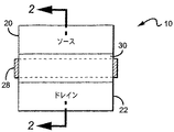
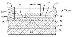
図1および2は、本発明による窒化物ベースの基板12を備えるHEMT10の一実施形態を示し、基板12は、シリコンカーバイド、サファイア、スピネット(spinet)、ZnO、シリコン、ガリウム窒化物、アルミニウム窒化物、またはIII族窒化物材料の成長をサポートすることができる任意の他の材料とすることができる。いくつかの実施形態で、基板12は、Durham,NCのCree,Inc.から商業的に入手可能な半絶縁性4H‐SiC からなることができる。
1 and 2 illustrate one embodiment of a
核生成層14が基板12上に生成され、基板12とHEMT10の次の層との間の格子不整合を低減することができる。核生成層14は、膜厚がおよそ1000オングストローム(Å)であるべきだが、他の膜厚を用いることもできる。核生成層14は、多くの異なる材料からなることができ、適切な材料はAlzGa1−zN(0≦z≦1)である。本発明による一実施形態で、核生成層はAlN(AlzGa1−zN,z=1)からなる。核生成層14は、有機金属気相成長法(MOCVD)、高蒸気圧エピタキシ(high vapor pressure epitaxy)(HVPE)、または分子線エピタキシ(MBE)などの既知の半導体成長技法を用いて基板12上に形成されることができる。さらに他の実施形態で、核生成層は、HEMT10内のバッファ層などの別の層の一部として形成されることができる(以下に詳細に説明する)。
A
核生成層14の形成は、基板12に用いられる材料に依存しうる。たとえば、様々な基板の上に核生成層14を形成する方法が特許文献2および3に教示されており、それぞれは本明細書で完全に記載されたかのように参照により組み込まれる。シリコンカーバイドの上に核生成層を形成する方法が特許文献4、5、および6に開示されており、それぞれは本明細書で完全に記載されたかのように参照により組み込まれる。
The formation of the
HEMT10は、核生成層14上に形成された高抵抗バッファ層16をさらに備え、適切なバッファ層16はAlxGayIn(1−x−y)N(0≦x≦1,0≦y≦1,x+y≦1)などのIII族窒化物材料からなる。本発明による別の実施形態で、バッファ層16は、膜厚およそ2μmで層の一部にFeがドープされたGaN層からなる。
The
バリア層18が、バッファ層16がバリア層18と核生成層14との間にはさまれるように、バッファ層上に形成されている。バッファ層16およびバリア層18のそれぞれは、ドープされた又はアンドープのIII族窒化物材料からなることができる。バリア層18は、InGaN、AlGaN、AlN、またはそれらの組み合わせなどの異なる材料の1つまたは複数の層からなることができる。一実施形態で、バリア層18は、0.8 nmのAlNおよび22.5 nmのAlxGa1−xN(フォトルミネッセンスによる測定でx≒0.195)からなる。例示的構造は、特許文献1、7、8、9、および10に示されており、それらのそれぞれは本明細書で完全に記載されたかのように参照により組み込まれる。他の窒化物ベースのHEMT構造は、特許文献11および12に示されており、それらのそれぞれは本明細書で完全に記載されたかのように参照により組み込まれる。バッファ層16およびバリア層18は、核生成層14の成長に用いられたのと同一の方法を用いてつくることができる。二次元電子ガス(2DEG)層/チャネル17が、バッファ層16とバリア層18との間のヘテロ界面に形成されている。デバイス間の電気的分離が、活性HEMTの外部でメサエッチまたはイオン注入によりなされている。
A
金属のソースコンタクト20およびドレインコンタクト22が形成され、バリア層18を通過してオーミックコンタクトをつくる。スペーサ層24が、ソースコンタクトとドレインコンタクトとの間のバリア層18の表面に形成されることができる。スペーサ層24は、誘電体(SiNまたはSiO)などの非導電性材料の1つの層、または異なる誘電体などの非導電性材料の複数の異なる層からなることができる。代替実施形態で、スペーサ層は、エピタキシャル材料の1つもしくは複数の層だけ、または誘電体材料の層との組み合わせからなることができる。スペーサ層は多くの異なる厚さとすることができ、適切な厚さの範囲はおよそ0.05から0.5ミクロンである。スペーサ層24は、主にフィールドプレートをその上に堆積できるように配置され、フィールドプレートはゲート26からドレインコンタクト22に向かって延びている。したがって、本発明によるいくつかの実施形態で、スペーサ層24はバリア層18の表面上のゲート26とドレインコンタクト22との間にのみ備えられることができる。
スペーサ層24がソースコンタクトとドレインコンタクトとの間のバリア層18を覆う実施形態で、スペーサ層24をバリア層18までエッチングし、ゲート電極26の底面がバリア層18の表面上にあるようにゲート電極26を堆積することができる。スペーサ層24がバリア層18の一部のみを覆う実施形態で、ゲート26をスペーサ層24に隣接してバリア層18上に堆積することができる。さらに他の実施形態で、ゲート26をスペーサ層24の前に堆積することができる。
In an embodiment where the
フィールドプレート28は、ゲート電極を形成している金属をパターニングし、ゲート26の上部がゲート26の端からドレイン22に向かって距離Lf延びているフィールドプレート構造28を形成するように、スペーサ層24にわたり延びているようにすることによって、ゲートの一部として形成されることができる。言い換えると、スペーサ層24上のゲート金属の一部が、フィールドプレート28を形成する。その構造は次に、シリコン窒化物などの誘電体パシベーション30により覆われることができる。誘電体パシベーション30を形成する方法は、上述の特許文献および非特許文献において詳細に説明されている。
ゲート26が適切なレベルにバイアスされているとき、ソートコンタクト20とドレインコンタクト22との間を2DEG層/チャネル17を介して電流が流れることができる。ソートコンタクト20およびドレインコンタクト22は、チタン、アルミニウム、金、またはニッケルの合金を含むがこれらに制限されない異なる材料から作られることができる。ゲート26もまた、金、ニッケル、白金、パラジウム、イリジウム、チタン、クロム、チタンとタングステンの合金、または白金シリサイドを含むがこれらに制限されない異なる材料から作られることができる。ゲート26は、多くの異なる長さをとることができ、ゲート長の適切な範囲は0.01から2ミクロンである。本発明による一実施形態で、好ましいゲート長(Lg)はおよそ0.5ミクロンである。いくつかの実施形態で、フィールドプレート28はゲート26の延長として同一の堆積ステップで形成される。他の実施形態で、フィールドプレート28およびゲート26は、別々の堆積ステップで形成される。ソースコンタクト20およびドレインコンタクト22の形成は、上述の特許文献および非特許文献に詳細に説明されている。
When
フィールドプレート28は、ゲート26の端からバリア層の上を異なる距離Lf延びていることができ、他の距離を用いることもできるが距離の適切な範囲は0.1から1.5μmである。フィールドプレート28は、多くの異なる導電性材料からなることができ、適切な材料はゲート26に用いられているのと同じ金属などの金属である。ゲート26およびフィールドプレート28は、標準的な配線形成(metallization)方法を用いて堆積することができる。
The
図3および4に、本発明による図1および2のHEMT10に類似するHEMT40の別の実施形態を示す。図3および4のHEMT40ならびにそれ以降の図面の同一または類似する特徴については、図1および2と同一の参照番号を用いる。HEMT40は、基板12、核生成層14、バッファ層16、2DEG17、バリア層18、ソースコンタクト20、およびドレインコンタクト22を備える。ゲート42が、バリア層18の形成の後に形成されている。スペーサ/パシベーション層44が、デバイス上に形成され、特に、ゲート42の上ならびにゲート42とソースコンタクト20およびドレインコンタクト22との間のバリア層18の表面に形成されている。他の実施形態で、スペーサ/パシベーション層44は、ゲート42の上およびゲート42とドレインコンタクト22との間のバリア層18の表面にのみ備えられることができる。次にフィールドプレート46がスペーサ/パシベーション層44上に形成され、ゲート42にオーバーラップしてゲート―ドレイン領域に距離Lf延びている。図3および4に示す実施形態で、スペーサ/パシベーション層44はフィールドプレート46に対するスペーサ層としての役割を果たす。ゲート42上のフィールドプレート46のオーバーラップは、最適な結果のために可変である。
FIGS. 3 and 4 illustrate another embodiment of a
フィールドプレート46はゲート42に電気的に接続されることができ、図3は、他の接続構造も用いることができることを理解されたいが、代替的ゲート構造を2つ示している。フィールドプレート46は、第1の導電性経路48を介してゲート42に接続されることができ、第1の導電性経路48は、HEMT40の活性領域の外を、ゲート42に電気的コンタクトをつくるのに用いられるゲートコンタクト50まで及んでいる。ゲートコンタクト50と反対側のHEMT40の活性領域の外にある(点線で示される)第2の導電性経路52も用いることができる。導電性経路52は、ゲート42とフィールドプレート46との間に結合(couple)されている。導電性ビア(via)(図示せず)も、フィールドプレート46をゲート42に接続させるのに用いることができ、ビアのそれぞれはパシベーション層44を通ってその2つの間を走っている。ビアをフィールドプレート46の下に周期的に配置することができ、それによってゲート42からフィールドプレート46への電流の効率的な広がりが提供される。
The
図1および2のHEMT10のように、フィールドプレート46はゲート42の端からバリア層の上を異なる距離Lf延びることができ、他の距離も用いることができるが距離の適切な範囲は0.1から1.5μmである。いくつかの実施形態で、フィールドプレート46は0.2から1μmの距離Lf延びることができる。他の実施形態で、フィールドプレート46は0.5から0.9μmの距離Lf延びることができる。好ましい実施形態で、フィールドプレート46はおよそ0.7μmの距離Lf延びることができる。
As in the
図5は、本発明によるHEMT60の別の実施形態を示していて、HEMT60は、基板12、核生成層14、バッファ層16、2DEG17、バリア層18、ソースコンタクト20、およびドレインコンタクト22を含む、HEMT10および40のそれらと類似した多くの特徴を有する。しかしながら、HEMT60は高周波数動作に特に適応したガンマ(Γ)型のゲートを有する。ゲート長はデバイスの速度の決定において重要なデバイス寸法の1つであり、高周波数デバイスではゲート長がより短い。短いゲートコンタクトは、高周波数動作に悪影響を与えうる高抵抗につながる。Tゲートが高周波数動作で一般に用いられるが、フィールドプレートのTゲートとのうまく結合した配置(well−coupled placement)を実現することは困難である可能性がある。
FIG. 5 shows another embodiment of a
ガンマゲート62は、低ゲート抵抗を可能にし、ゲートのフットプリント(footprint)の制御された限定を可能にする。スペーサ/パシベーション層64が備えられ、これは、ガンマゲート62ならびにガンマゲート62とソースコンタクト20およびドレインコンタクト22との間のバリア層18の表面を覆う。ガンマゲート62の水平部分とスペーサ層の上部との間にスペースが残りうる。HEMT60は、ガンマゲート62をオーバーラップするスペーサ層64上のフィールドプレート66も備え、フィールドプレート66は好ましくは、水平に覆いかぶさる部分がなくガンマゲートの側面に堆積されている。この配置は、密接な配置およびフィールドプレートとその下の活性層との有効な結合を可能にする。
The gamma gate 62 allows for low gate resistance and allows for a controlled limitation of the gate footprint. A spacer /
図3および4に示され、上に説明されたフィールドプレート46のように、フィールドプレート66はゲート62に多くの異なる方法で電気的に接続されることができる。第1の伝導性経路(図示せず)がフィールドプレート66とゲートコンタクトとの間に備えられることができ、または第2の伝導性経路(図示せず)がフィールドプレート66とゲート62との間に備えられることができ、伝導性経路の両方はHEMTの活性領域の外にある。スペーサ層64を通過する伝導性ビアをフィールドプレート66とゲート62との間に用いることもできる。
Like the
図6は、本発明による図1に示したHEMT10に類似するHEMT80の別の実施形態を示していて、同様に基板12、核生成層14、バッファ層16、2DEG17、バリア層18、ソースコンタクト20、ドレインコンタクト22、スペーサ層24、およびフィールドプレート構造28を有するゲート26を備える。HEMT80は、スペーサ層24上に形成された、n+ドープされたコンタクト層82も備える。ゲートコンタクト26の形成前に、コンタクト層82はエッチングされ、スペーサ層24の表面の一部が見えるようになる。次に、スペーサ層24のさらに小さな一部がバリア層18までエッチングされることができる。また、コンタクト層82、スペーサ層24、およびバリア層は、ソースコンタクト20およびドレインコンタクト22を堆積できるようにバッファ層16までエッチングされることができる。コンタクト層82は、低アクセス領域抵抗を提供することに加えて、オーミックなソースコンタクト20およびドレインコンタクト22の形成を促進する。
FIG. 6 shows another embodiment of a
図7は本発明によるHEMT90の別の実施形態を示していて、上で説明したHEMTのそれらと類似する基板12、核生成層14、バッファ層16、2DEG17、バリア層18、ソースコンタクト20、およびドレインコンタクト22を備える。HEMT90は、ゲート92およびフィールドプレート94も備える。しかしながら、HEMT90は1つのスペーサ層を有する代わりに、より多くのスペーサ層を用いることができることを理解されたいが、この場合では2つの複数のスペーサ層95を備える。第1のスペーサ層96が、少なくともゲート92とドレインコンタクト22との間のバリア層18の上に形成され、好ましいスペーサ層はゲート92とソースコンタクト20との間のバリア層18の上にもある。第2のスペーサ層98が第1のスペーサ層96の上に形成され、多くの異なる方法で配置することができる。第2のスペーサ層98は、好ましくは第1のスペーサ層96の上部表面のすべては覆わずに、ステップ100を形成する。フィールドプレート94はスペーサ層上に形成され、フィールドプレート94はステップ100のために本質的に第1および第2のフィールドプレート部分102、104を備え、これらのそれぞれはそれとバリア層18との間に異なる間隔を有する。
FIG. 7 shows another embodiment of a
第1および第2のスペーサ層96、98は多くの異なる材料からなることができ、一般的にはこれらの層はエピタキシャル材料またはSiNおよびSiOなどの誘電体材料からなる。本発明による一実施形態で、第1のスペーサ層96をエピタキシャル材料として、第2のスペーサ層98を誘電体材料とすることができる。別の実施形態で、第1のスペーサ層96を再びエピタキシャル材料として、第2のスペーサ層98もまた第1のスペーサ層96と同一または異なる材料のエピタキシャル材料とすることができる。第1のスペーサ層が誘電体材料からなり、第2のスペーサ層がエピタキシャル材料からなるようにすることもできるが、用いられる誘電体材料のタイプによっては結晶構造の喪失のために第2の(エピタキシャル)層98を形成することが困難になりうる。エピタキシャル材料を用いることでより良いフィールドプレート結合(field plate coupling)が一般的に提供されるが、エピタキシャル材料により導入されるキャパシタンスは誘電体材料のそれよりも大きくなりうる。
The first and second spacer layers 96, 98 can be made of many different materials, typically these layers are made of an epitaxial material or a dielectric material such as SiN and SiO. In one embodiment according to the present invention, the
第1および第2のフィールドプレート102、104を有することにより、HEMT90は2つの異なる電圧で改善された動作特性を示すことができ、第1のフィールドプレート102がHEMT90の改善された動作をある電圧で可能にし、第2のフィールドプレート104がより高い第2の電圧で改善された動作を可能にする。たとえば、第1のスペーサ層102がエピタキシャル(一般にはAlGaNまたは同様の材料)であるHEMT90の実施形態で、第1のフィールドプレート102の下の層102の物理的寸法および誘電率は一定である。一定の寸法および誘電率は、第1のフィールドプレートがHEMT90の改善された動作特性を第1の電圧で提供することを可能にする。
By having the first and
第2の層98が誘電体材料で作られている場合、その誘電体材料は一般に第1の層96のエピタキシャル材料よりも低い誘電率を有する。結果として、第2のフィールドプレート104の下の材料の全体の誘電率は、第1のフィールドプレート102の下の材料の誘電率より低くなる。このことは、低いキャパシタンスおよび低減されたカップリングという結果を生じさせる。低い誘電率に加えて第2のフィールドプレート104とバリア層18との間のより大きな距離は、第2のフィールドプレート104がより高い電圧で改善された動作特性を提供するという結果を生じさせる。
When the
第1および第2の層96、98がエピタキシャルで、第1および第2のフィールドプレート102、104の下の誘電率が同一であるが、第2のフィールドプレート104とバリア層18との間の距離が大きくなっているようなHEMT90の実施形態においてでも、より高い電圧で改善された動作特性が提供される。しかしながら、より高い動作電圧は、第2のスペーサ材料が誘電体材料であった場合とは一般に異なる。
The first and
ゲート92、フィールドプレート102、104、およびスペーサ層94、96は多くの異なる方法で形成されることができ、1つの形成方法は第1の(エピタキシャル)スペーサ層94をバリア層18上に堆積し、次にバリア層をエッチングしてゲート92のためのスペースを設けることである。次に、ゲート92を堆積することができ、第2のスペーサ層96を第1の層96の上に堆積することができる。他の実施形態で、第2のスペーサ層96はゲート92の堆積前にエッチングされることができる。あるいは、第1および第2のスペーサ層96、98を堆積し、次に2つのエッチングステップでエッチングすることができる。第1のエッチングは両方の層96、98を通してであり、第2のエッチングはステップ100を形成するために第2の層98を通してである。ゲート92を次に堆積し、フィールドプレート102、104を第1のスペーサ96および第2のスペーサ98の上に次に堆積することができる。あるいは、第1および第2のスペーサ層96、98を形成し、次にエッチングすることができ、ゲート92およびフィールドプレートは1つまたは複数の形成ステップで形成される。さらに他の実施形態で、エピタキシャルまたは誘電体材料からなる単一のスペーサ層をエッチングし、結果として生じるフィールドプレートが第1および第2の部分を有するようなステップを提供することができる。
The
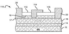
本発明によるゲートおよびフィールドプレート構造は、図1〜7に示されている形を越えて多くの異なる方法で用いることができる。図8、9、および10はHEMT110、130、および140をそれぞれ示し、各HEMTは上で説明したHEMTのそれらと類似する基板12、核生成層14、バッファ層16、2DEG17、バリア層18、ソースコンタクト20、およびドレインコンタクト22を備える。HEMT110(図8)は、ゲート112がバリア層18内にリセス化されて(recessed)いることを除いて、図1および2のHEMT10に類似する。HEMTのフィールドプレート114はスペーサ層116上に堆積されていて、ゲート112からドレインコンタクト22に向かって延びている。フィールドプレート114は、HEMT10のフィールドプレート28と同一の動作改善を提供する。HEMT130(図9)は、ゲート132がリセス化されていることを除いて、図3および4のHEMT10に類似する。フィールドプレート134はスペーサ層136上に堆積されていて、同一の動作利益を提供する。本明細書に説明されるHEMTは、部分的にのみリセス化されているゲートを備えることができる。HEMT140は、ゲート142が部分的にリセス化されていることを除いて、HEMT130に類似する。そのフィールドプレート144はスペーサ層146上に堆積されていて、同一の動作利益を提供する。
The gate and field plate structure according to the present invention can be used in many different ways beyond the shape shown in FIGS. 8, 9, and 10 show
図11は、本発明によるさらに別の実施形態のHEMT150を示していて、基板12、核生成層14、バッファ層16、2DEG17、バリア層18、ソースコンタクト20、およびドレインコンタクト22を有する。HEMT150はゲート152、スペーサ層154、およびゲートの一部であるフィールドプレート156も有する。HEMT150はさらに、フィールドプレート156を覆う第2のスペーサ層158、スペーサ層154、およびスペーサ層154より上の部分のゲート152を備える。第2のフィールドプレート159は、第2のスペーサ層158の上にあり、一般にゲート152からドレイン22に向かって延びていて、第2のフィールドプレートは第2のスペーサ層158を通る1つまたは複数のビアにより(図示せず)、またはHEMT150の活性領域の外に形成されている1つまたは複数の導電性経路によりゲートに電気的に結合されている。本発明による他のHEMTは、追加のスペーサ層とフィールドプレートの対を備えることができ、1つの追加の対が点線で示されている。構造は、誘電体パシベーション層(図示せず)により覆われることもできる。
FIG. 11 shows yet another embodiment of a
図3および4の実施形態によるGaNベースのHEMT構造が構築され、テストされた。その結果が図12のグラフ160に示されている。当初のテストでは、51 %の付加電力効率(PAE)で20.4 W/mmの電力密度が示され、82 Vおよび42 GHzでクラスBで動作した。より最近のテストでは、82 Vおよび42 GHzで55 %のPAEで32 W/mmの電力密度の改善された性能が達成された。
A GaN-based HEMT structure according to the embodiment of FIGS. 3 and 4 was constructed and tested. The result is shown in the
デバイス性能に対するフィールドプレート距離(Lf)の効果がテストされた。フィールドプレート長Lfが0から0.9μmの距離まで変えられ、ついでその結果であるデバイスのPAEが測定された。図12に示すように、PAEはフィールドプレート長が0.5μmまで延ばされると改善を示し、最適な長さはだいたい0.7μmであった。しかしながら、最適な長さは動作電圧および周波数に加えて特定のデバイスデザインにも依存しうる。 The effect of field plate distance (L f ) on device performance was tested. The field plate length L f was varied from 0 to a distance of 0.9 μm, and the resulting device PAE was then measured. As shown in FIG. 12, PAE showed improvement when the field plate length was extended to 0.5 μm, and the optimum length was approximately 0.7 μm. However, the optimum length may depend on the specific device design as well as the operating voltage and frequency.
上で説明したフィールドプレート配置は他のタイプのトランジスタにおいて用いることができる。図13は、本発明による金属半導体接合FET(MESFET)の一実施形態を示していて、MESFETは、他の材料系のMESFETも用いることができるが、好ましくはシリコンカーバイド(SiC)ベースである。MESFET170は、シリコンカーバイドバッファ174およびシリコンカーバイドチャネル層176が形成されているシリコンカーバイド基板を備え、バッファ174はチャネル層176と基板172との間にはさまれている。ソースコンタクト178およびドレインコンタクト180がチャネル176と接触して形成されている。
The field plate arrangement described above can be used in other types of transistors. FIG. 13 illustrates one embodiment of a metal semiconductor junction FET (MESFET) according to the present invention, which is preferably silicon carbide (SiC) based, although other material-based MESFETs may be used. The
非導電性スペーサ層182が、チャネル層176上にソースコンタクト178とドレインコンタクト180との間に形成されている。上で説明し、図1および2に示したスペーサ層24のように、スペーサ層182は、誘電体などの非導電性材料の層、または異なる誘電体もしくはエピタキシャル材料などの複数の異なる非導電性材料の層を備えることができる。
A
また、図1および2のスペーサ層24のように、スペーサ層182はチャネル層176までエッチングされることができ、ゲート184が、ゲート184の底面がチャネル層176の表面上にあるように堆積されることができる。ゲート184を形成している金属は、スペーサ層182にわたって延びているようにパターニングし、それによりゲート184の上部がゲート184の端からドレインコンタクト180に向かって距離Lf延びているフィールドプレート構造186を形成するようにされることができる。最後に、この構造はシリコン窒化物などの誘電体パシベーション層188によって覆われることができる。
Also, like the
シリコンカーバイドベースのMESFETデバイスの作製については、特許文献13および14に詳細に説明されていて、それぞれが本明細書に参照によって全体として組み込まれている。 The fabrication of silicon carbide based MESFET devices is described in detail in US Pat.
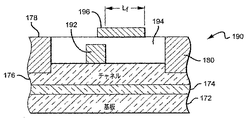
図14は、本発明による別の実施形態のMESFET190を示し、MESFET190は、図12のMESFET170に類似するが、図3および4に示されたHEMT40のそれらに類似するゲートおよびフィールドプレート構造を有する。MESFET190は、シリコンカーバイド基板172、バッファ174、およびチャネル176を備える。さらに、ソースコンタクト178、ドレインコンタクト180、およびチャネル176に堆積されたゲート192も備える。スペーサ層194が、ゲート192の上ならびにゲート192とソースコンタクト178およびドレインコンタクト180との間のチャネル176の表面に堆積されている。フィールドプレート186がスペーサ層194上に堆積され、ゲート192にオーバーラップしている。フィールドプレート196は、上で説明した図3および4のHEMT40の導電性経路によってゲート192にカップリングされている。共にMESFETの活性領域の外を走る、ゲートコンタクトへの第1の導電性経路(図示せず)またはゲート192への第2の導電性経路(図示せず)を含む、多くの異なる導電性経路を用いることができる。フィールドプレート196は、スペーサ層194を通る導電性ビア(図示せず)によってゲート192に結合されることもできる。
FIG. 14 shows another embodiment of
ちょうど上述のHEMTのように、本発明によるMESFETの異なる実施形態は、リセス化されているゲートを備えることができる。図15は、本発明によるMESFET200の一実施形態を示し、リセス化されているゲート202を有する。図12および13のMESFET170および190のように、MESFET200も、シリコンカーバイド基板172、バッファ174、チャネル176、ソースコンタクト178、およびドレインコンタクト180を備える。ゲート202は、チャネル176の上に堆積されている。スペーサ層204が、ゲート202の上ならびにゲート202とソースコンタクト178およびドレインコンタクト180との間のチャネル176の表面に堆積されている。スペーサ層204は、よりゲート202の形に合致するように図14のスペーサ層194よりも薄い。ゲート202はチャネル176内に部分的にリセス化されていて、フィールドプレート206はスペーサ層204上に堆積され、ゲート202にオーバーラップしている。フィールドプレート206は、図3および4のHEMT40で説明されたような1つまたは複数の導電性経路によってゲート202に結合されている。
Just like the HEMT described above, different embodiments of the MESFET according to the present invention may comprise a recessed gate. FIG. 15 illustrates one embodiment of a
また、本発明によるMESFETの異なる実施形態は、図7のHEMT90で説明されたような複数のスペーサ層を備えることができることを理解されたい。本発明によるいくつかの実施形態で、MESFETは、2つ以上の層を用いることもできるが、ステップ配置の2つのスペーサ層を有することができる。これらの層は、これも上で説明したように、エピタキシャルまたは誘電体材料からなることができ、ステップ配置は2つの電圧で改善された動作特性を提供する2つのフィールドプレートを効率的に提供する。本発明によるMESFETは、図11に示し、上で説明したHEMT150に類似した複数のスペーサ層およびフィールドプレートを備えることができることを理解されたい。
It should also be understood that different embodiments of MESFETs according to the present invention can comprise multiple spacer layers as described in
本発明は、その特定の好ましい構成を参照して相当に詳細に説明してきたが、他のバージョンが可能である。フィールドプレート配置は、多くの異なるデバイスで用いることができる。フィールドプレートは、また、多くの異なる形を有することができ、多くの異なる方法によりソースコンタクトに接続されることができる。したがって、本発明の精神および範囲は、上で説明した本発明の好ましいバージョンに制限されるべきではない。 Although the present invention has been described in considerable detail with reference to certain preferred configurations thereof, other versions are possible. The field plate arrangement can be used with many different devices. The field plate can also have many different shapes and can be connected to the source contact in many different ways. Accordingly, the spirit and scope of the present invention should not be limited to the preferred versions of the present invention described above.
Claims (38)
前記複数の活性層との電気的コンタクトで形成されたソースコンタクトと、
前記複数の活性層との電気的コンタクトで同様に形成されたドレインコンタクトであって、前記複数の活性層の最上部の上の前記ソースコンタクトと前記ドレインコンタクトとの間にスペースがあるドレインコンタクトと、
前記ソースコンタクトと前記ドレインコンタクトとの間の前記複数の活性層の前記最上部との電気的コンタクトで形成されたゲートと、
前記ゲートと前記ドレインコンタクトとの間の前記複数の活性層の最上部の表面に形成されたエピタキシャル材料のスペーサ層であって、前記ゲートは前記スペーサ層により覆われていないスペーサ層と、
前記スペーサ層の上に前記ゲートの一部として形成されたフィールドプレートと
を備えることを特徴とするトランジスタ。 A plurality of active semiconductor layers formed on a substrate;
A source contact formed by electrical contact with the plurality of active layers;
A drain contact formed similarly in electrical contact with the plurality of active layers, the drain contact having a space between the source contact and the drain contact on the top of the plurality of active layers; ,
A gate formed in electrical contact with the top of the plurality of active layers between the source contact and the drain contact;
A spacer layer of epitaxial material formed on the uppermost surface of the plurality of active layers between the gate and the drain contact, wherein the gate is not covered by the spacer layer; and
And a field plate formed as part of the gate on the spacer layer.
前記複数の活性層との電気的コンタクトで形成されたソースコンタクトと、
前記複数の活性層との電気的コンタクトで同様に形成されたドレインコンタクトであって、前記複数の活性層の最上部の上の前記ソースコンタクトと前記ドレインコンタクトとの間にスペースがあるドレインコンタクトと、
前記ソースコンタクトと前記ドレインコンタクトとの間の前記複数の活性層の前記最上部との電気的コンタクトで形成されたゲートと、
前記ゲートと前記ドレインコンタクトとの間の前記複数の活性層の最上部の表面に形成された、前記ゲートコンタクトを覆うスペーサ層と、
前記スペーサ層の上に形成され、前記ゲートに電気的に接続されているフィールドプレートと
を備えることを特徴とするトランジスタ。 A plurality of active semiconductor layers formed on a substrate;
A source contact formed by electrical contact with the plurality of active layers;
A drain contact formed similarly in electrical contact with the plurality of active layers, the drain contact having a space between the source contact and the drain contact on the top of the plurality of active layers; ,
A gate formed in electrical contact with the top of the plurality of active layers between the source contact and the drain contact;
A spacer layer formed on the top surface of the plurality of active layers between the gate and the drain contact, covering the gate contact;
And a field plate formed on the spacer layer and electrically connected to the gate.
前記活性層との電気的コンタクトで形成された金属のソースコンタクトおよびドレインコンタクトと、
前記活性層内の電界を変調するための前記ソースコンタクトと前記ドレインコンタクトとの間に形成されたゲートコンタクトと、
前記活性層の上に形成されたスペーサ層と、
前記スペーサ層の上に形成され、前記ゲートコンタクトの端から前記ドレインコンタクトに向かって距離Lf延びている、前記ゲートコンタクトに電気的に接続されている導電性フィールドプレートと
を備えることを特徴とするトランジスタ構造。 An active semiconductor layer;
Metal source and drain contacts formed in electrical contact with the active layer;
A gate contact formed between the source contact and the drain contact for modulating an electric field in the active layer;
A spacer layer formed on the active layer;
And characterized in that it comprises are formed on the spacer layer, the extending end distance L f toward said drain contact from the gate contact, and a conductive field plate is electrically connected to the gate contact Transistor structure.
前記活性層との電気的コンタクトで形成された金属のソースコンタクトおよびドレインコンタクトと、
前記活性層内の電界を変調するための前記ソースコンタクトと前記ドレインコンタクトとの間に形成されたゲートコンタクトと、
前記活性半導体層の上の前記スペーサの上に形成され、前記ゲートコンタクトの端から前記ドレインコンタクトに向かって距離Lf延びている導電性フィールドプレートであって、前記ゲートコンタクトに電気的に接続されていて、前記フィールドプレートを有しない類似のトランジスタと比較して前記トランジスタ内のピーク動作電界の低減を提供するフィールドプレートと
を備えることを特徴とするトランジスタ。 An active semiconductor layer;
Metal source and drain contacts formed in electrical contact with the active layer;
A gate contact formed between the source contact and the drain contact for modulating an electric field in the active layer;
Wherein formed on the spacer on the active semiconductor layer, wherein a conductive field plate from the edge of the gate contact extends a distance L f toward said drain contact, are electrically connected to the gate contact And a field plate that provides a reduction in peak operating field in the transistor as compared to a similar transistor without the field plate.
前記複数の活性層との電気的コンタクトで形成されたソースコンタクトおよびドレインコンタクトと、
前記ソースコンタクトと前記ドレインコンタクトとの間の前記複数の活性層の前記最上部との電気的コンタクトで形成されたゲートと、
前記ゲートと前記ドレインコンタクトとの間の前記複数の活性層の前記最上部の表面に形成された第1のスペーサ層であって、前記ゲートは前記スペーサ層によって覆われていない第1のスペーサ層と、
前記ゲートの一部として前記スペーサ層の上に形成され、前記ドレインコンタクトに向かって前記スペーサ層の上を延びている第1のフィールドプレートと、
前記フィールドプレートおよび前記フィールドプレートと前記ドレインコンタクトとの間の前記スペーサ層の表面を覆っている第2のスペーサ層と
を備え、さらに、前記第2のスペーサ層の上にあり、前記ゲートの端から前記ドレインコンタクトに向かって延びている第2のフィールドプレートを備えることを特徴とするトランジスタ。 A plurality of active semiconductor layers formed on the substrate;
A source contact and a drain contact formed by electrical contact with the plurality of active layers;
A gate formed in electrical contact with the top of the plurality of active layers between the source contact and the drain contact;
A first spacer layer formed on the uppermost surface of the plurality of active layers between the gate and the drain contact, wherein the gate is not covered by the spacer layer; When,
A first field plate formed on the spacer layer as part of the gate and extending over the spacer layer toward the drain contact;
A second spacer layer covering the surface of the spacer layer between the field plate and the field plate and the drain contact, and further over the second spacer layer, and an end of the gate A transistor comprising: a second field plate extending from to the drain contact.
前記バッファ層の上のチャネル層と、
前記チャネル層との電気的コンタクトで形成されたソースおよびドレインコンタクトと、
前記ソースコンタクトと前記ドレインコンタクトとの間に前記チャネル層との電気的コンタクトで形成されたゲートと、
少なくとも前記ゲートと前記ドレインコンタクトとの間の前記チャネル層の表面に形成されたスペーサ層と、
前記ゲートとの電気的コンタクトでスペーサ層の上に形成されたフィールドプレートと
を備えることを特徴とする金属半導体接合FET(MESFET)。
A buffer layer on the substrate;
A channel layer on the buffer layer;
Source and drain contacts formed in electrical contact with the channel layer;
A gate formed in electrical contact with the channel layer between the source contact and the drain contact;
A spacer layer formed on the surface of the channel layer at least between the gate and the drain contact;
And a field plate formed on the spacer layer in electrical contact with the gate. A metal semiconductor junction FET (MESFET).
Applications Claiming Priority (3)
| Application Number | Priority Date | Filing Date | Title |
|---|---|---|---|
| US50157603P | 2003-09-09 | 2003-09-09 | |
| US10/930,160 US7501669B2 (en) | 2003-09-09 | 2004-08-31 | Wide bandgap transistor devices with field plates |
| PCT/US2004/029345 WO2005029589A1 (en) | 2003-09-09 | 2004-09-08 | Wide bandgap transistor devices with field plates |
Publications (2)
| Publication Number | Publication Date |
|---|---|
| JP2007505501A true JP2007505501A (en) | 2007-03-08 |
| JP2007505501A5 JP2007505501A5 (en) | 2007-09-06 |
Family
ID=34228870
Family Applications (1)
| Application Number | Title | Priority Date | Filing Date |
|---|---|---|---|
| JP2006526270A Pending JP2007505501A (en) | 2003-09-09 | 2004-09-08 | Wide band gap transistor device with field plate |
Country Status (7)
| Country | Link |
|---|---|
| US (4) | US7501669B2 (en) |
| EP (4) | EP1665385B1 (en) |
| JP (1) | JP2007505501A (en) |
| KR (1) | KR101108300B1 (en) |
| CN (2) | CN102306658A (en) |
| CA (1) | CA2536030A1 (en) |
| WO (1) | WO2005029589A1 (en) |
Cited By (11)
| Publication number | Priority date | Publication date | Assignee | Title |
|---|---|---|---|---|
| JP2008535241A (en) * | 2005-04-01 | 2008-08-28 | レイセオン・カンパニー | Semiconductor device with improved field plate |
| JP2009021362A (en) * | 2007-07-11 | 2009-01-29 | Sumitomo Electric Ind Ltd | Group iii nitride electronic device, laminate wafer for group iii nitride electronic device, and method of manufacturing group iii nitride electronic device |
| JP2010538582A (en) * | 2007-09-07 | 2010-12-09 | レイセオン カンパニー | Input circuit for a transistor power amplifier and method for designing such a circuit |
| JP2013503483A (en) * | 2009-08-28 | 2013-01-31 | トランスフォーム インコーポレーテッド | Semiconductor device having field plate |
| JP2013141000A (en) * | 2007-03-23 | 2013-07-18 | Cree Inc | Semiconductor device |
| JP2014090037A (en) * | 2012-10-29 | 2014-05-15 | Advanced Power Device Research Association | Semiconductor device |
| US9419124B2 (en) | 2001-07-24 | 2016-08-16 | Cree, Inc. | Insulating gate AlGaN/GaN HEMT |
| US9935190B2 (en) | 2014-07-21 | 2018-04-03 | Transphorm Inc. | Forming enhancement mode III-nitride devices |
| US10043898B2 (en) | 2013-03-13 | 2018-08-07 | Transphorm Inc. | Enhancement-mode III-nitride devices |
| US10224401B2 (en) | 2016-05-31 | 2019-03-05 | Transphorm Inc. | III-nitride devices including a graded depleting layer |
| US11322599B2 (en) | 2016-01-15 | 2022-05-03 | Transphorm Technology, Inc. | Enhancement mode III-nitride devices having an Al1-xSixO gate insulator |
Families Citing this family (177)
| Publication number | Priority date | Publication date | Assignee | Title |
|---|---|---|---|---|
| TWI430341B (en) * | 2003-09-09 | 2014-03-11 | Univ California | Fabrication of single or multiple gate field plates |
| US7501669B2 (en) | 2003-09-09 | 2009-03-10 | Cree, Inc. | Wide bandgap transistor devices with field plates |
| TWI295085B (en) * | 2003-12-05 | 2008-03-21 | Int Rectifier Corp | Field effect transistor with enhanced insulator structure |
| US7045404B2 (en) * | 2004-01-16 | 2006-05-16 | Cree, Inc. | Nitride-based transistors with a protective layer and a low-damage recess and methods of fabrication thereof |
| US8174048B2 (en) * | 2004-01-23 | 2012-05-08 | International Rectifier Corporation | III-nitride current control device and method of manufacture |
| US7573078B2 (en) | 2004-05-11 | 2009-08-11 | Cree, Inc. | Wide bandgap transistors with multiple field plates |
| US7550783B2 (en) | 2004-05-11 | 2009-06-23 | Cree, Inc. | Wide bandgap HEMTs with source connected field plates |
| US9773877B2 (en) * | 2004-05-13 | 2017-09-26 | Cree, Inc. | Wide bandgap field effect transistors with source connected field plates |
| US20060073621A1 (en) * | 2004-10-01 | 2006-04-06 | Palo Alto Research Center Incorporated | Group III-nitride based HEMT device with insulating GaN/AlGaN buffer layer |
| US9640649B2 (en) * | 2004-12-30 | 2017-05-02 | Infineon Technologies Americas Corp. | III-nitride power semiconductor with a field relaxation feature |
| JP4845872B2 (en) * | 2005-01-25 | 2011-12-28 | 富士通株式会社 | Semiconductor device having MIS structure and manufacturing method thereof |
| US11791385B2 (en) | 2005-03-11 | 2023-10-17 | Wolfspeed, Inc. | Wide bandgap transistors with gate-source field plates |
| US7615774B2 (en) * | 2005-04-29 | 2009-11-10 | Cree.Inc. | Aluminum free group III-nitride based high electron mobility transistors |
| US20060255377A1 (en) * | 2005-05-12 | 2006-11-16 | Der-Wei Tu | Field effect transistor with novel field-plate structure |
| WO2006132419A1 (en) * | 2005-06-10 | 2006-12-14 | Nec Corporation | Field effect transistor |
| US7863648B2 (en) * | 2005-06-10 | 2011-01-04 | Nec Corporation | Field effect transistor |
| US20070018199A1 (en) * | 2005-07-20 | 2007-01-25 | Cree, Inc. | Nitride-based transistors and fabrication methods with an etch stop layer |
| US7548112B2 (en) * | 2005-07-21 | 2009-06-16 | Cree, Inc. | Switch mode power amplifier using MIS-HEMT with field plate extension |
| US8183595B2 (en) * | 2005-07-29 | 2012-05-22 | International Rectifier Corporation | Normally off III-nitride semiconductor device having a programmable gate |
| JP4751150B2 (en) | 2005-08-31 | 2011-08-17 | 株式会社東芝 | Nitride semiconductor devices |
| JP5501618B2 (en) * | 2005-09-07 | 2014-05-28 | クリー インコーポレイテッド | High electron transfer transistor (HEMT), semiconductor device and manufacturing method thereof |
| WO2007136401A2 (en) * | 2005-09-16 | 2007-11-29 | The Regents Of The University Of California | N-polar aluminum gallium nitride/gallium nitride enhancement-mode field effect transistor |
| US20070138515A1 (en) * | 2005-12-19 | 2007-06-21 | M/A-Com, Inc. | Dual field plate MESFET |
| JP2009522812A (en) * | 2006-01-09 | 2009-06-11 | インターナショナル レクティファイアー コーポレイション | Group III nitride power semiconductor with electric field relaxation function |
| US7709269B2 (en) | 2006-01-17 | 2010-05-04 | Cree, Inc. | Methods of fabricating transistors including dielectrically-supported gate electrodes |
| US7592211B2 (en) * | 2006-01-17 | 2009-09-22 | Cree, Inc. | Methods of fabricating transistors including supported gate electrodes |
| DE112007000667T5 (en) * | 2006-03-20 | 2009-01-29 | International Rectifier Corp., El Segundo | Unified gate cascode transistor |
| US7408208B2 (en) * | 2006-03-20 | 2008-08-05 | International Rectifier Corporation | III-nitride power semiconductor device |
| US7388236B2 (en) * | 2006-03-29 | 2008-06-17 | Cree, Inc. | High efficiency and/or high power density wide bandgap transistors |
| KR100770132B1 (en) * | 2006-10-30 | 2007-10-24 | 페어차일드코리아반도체 주식회사 | Gan semiconductor device |
| US8283699B2 (en) * | 2006-11-13 | 2012-10-09 | Cree, Inc. | GaN based HEMTs with buried field plates |
| US7692263B2 (en) | 2006-11-21 | 2010-04-06 | Cree, Inc. | High voltage GaN transistors |
| JP4712683B2 (en) * | 2006-12-21 | 2011-06-29 | パナソニック株式会社 | Transistor and manufacturing method thereof |
| US7838904B2 (en) * | 2007-01-31 | 2010-11-23 | Panasonic Corporation | Nitride based semiconductor device with concave gate region |
| JP4691060B2 (en) * | 2007-03-23 | 2011-06-01 | 古河電気工業株式会社 | GaN-based semiconductor devices |
| US20090072269A1 (en) * | 2007-09-17 | 2009-03-19 | Chang Soo Suh | Gallium nitride diodes and integrated components |
| US7915643B2 (en) | 2007-09-17 | 2011-03-29 | Transphorm Inc. | Enhancement mode gallium nitride power devices |
| US7800132B2 (en) * | 2007-10-25 | 2010-09-21 | Northrop Grumman Systems Corporation | High electron mobility transistor semiconductor device having field mitigating plate and fabrication method thereof |
| US8039301B2 (en) * | 2007-12-07 | 2011-10-18 | The United States Of America As Represented By The Secretary Of The Navy | Gate after diamond transistor |
| US7750370B2 (en) * | 2007-12-20 | 2010-07-06 | Northrop Grumman Space & Mission Systems Corp. | High electron mobility transistor having self-aligned miniature field mitigating plate on a protective dielectric layer |
| JP5134378B2 (en) * | 2008-01-07 | 2013-01-30 | シャープ株式会社 | Field effect transistor |
| US7965126B2 (en) | 2008-02-12 | 2011-06-21 | Transphorm Inc. | Bridge circuits and their components |
| US8519438B2 (en) | 2008-04-23 | 2013-08-27 | Transphorm Inc. | Enhancement mode III-N HEMTs |
| CN101604704B (en) * | 2008-06-13 | 2012-09-05 | 西安能讯微电子有限公司 | HEMT device and manufacturing method thereof |
| US7985986B2 (en) | 2008-07-31 | 2011-07-26 | Cree, Inc. | Normally-off semiconductor devices |
| JP5408929B2 (en) | 2008-08-21 | 2014-02-05 | 昭和電工株式会社 | Semiconductor device and manufacturing method of semiconductor device |
| US8289065B2 (en) | 2008-09-23 | 2012-10-16 | Transphorm Inc. | Inductive load power switching circuits |
| US7898004B2 (en) | 2008-12-10 | 2011-03-01 | Transphorm Inc. | Semiconductor heterostructure diodes |
| US7884394B2 (en) * | 2009-02-09 | 2011-02-08 | Transphorm Inc. | III-nitride devices and circuits |
| US8823012B2 (en) * | 2009-04-08 | 2014-09-02 | Efficient Power Conversion Corporation | Enhancement mode GaN HEMT device with gate spacer and method for fabricating the same |
| US8742459B2 (en) | 2009-05-14 | 2014-06-03 | Transphorm Inc. | High voltage III-nitride semiconductor devices |
| JP5595685B2 (en) * | 2009-07-28 | 2014-09-24 | パナソニック株式会社 | Semiconductor device |
| US8138529B2 (en) | 2009-11-02 | 2012-03-20 | Transphorm Inc. | Package configurations for low EMI circuits |
| JP5625336B2 (en) * | 2009-11-30 | 2014-11-19 | サンケン電気株式会社 | Semiconductor device |
| JP5037594B2 (en) * | 2009-12-08 | 2012-09-26 | シャープ株式会社 | Field effect transistor |
| US8389977B2 (en) | 2009-12-10 | 2013-03-05 | Transphorm Inc. | Reverse side engineered III-nitride devices |
| US8816497B2 (en) | 2010-01-08 | 2014-08-26 | Transphorm Inc. | Electronic devices and components for high efficiency power circuits |
| US8624662B2 (en) * | 2010-02-05 | 2014-01-07 | Transphorm Inc. | Semiconductor electronic components and circuits |
| US20110241020A1 (en) * | 2010-03-31 | 2011-10-06 | Triquint Semiconductor, Inc. | High electron mobility transistor with recessed barrier layer |
| US8907350B2 (en) * | 2010-04-28 | 2014-12-09 | Cree, Inc. | Semiconductor devices having improved adhesion and methods of fabricating the same |
| EP2383786B1 (en) | 2010-04-29 | 2018-08-15 | Ampleon Netherlands B.V. | Semiconductor transistor comprising two electrically conductive shield elements |
| US8829999B2 (en) | 2010-05-20 | 2014-09-09 | Cree, Inc. | Low noise amplifiers including group III nitride based high electron mobility transistors |
| JP2011249728A (en) * | 2010-05-31 | 2011-12-08 | Toshiba Corp | Semiconductor device and method for manufacturing the same |
| US8809987B2 (en) * | 2010-07-06 | 2014-08-19 | The Hong Kong University Of Science And Technology | Normally-off III-nitride metal-2DEG tunnel junction field-effect transistors |
| JP5655424B2 (en) * | 2010-08-09 | 2015-01-21 | サンケン電気株式会社 | Compound semiconductor device |
| JP2012109492A (en) * | 2010-11-19 | 2012-06-07 | Sanken Electric Co Ltd | Compound semiconductor device |
| JP5707903B2 (en) * | 2010-12-02 | 2015-04-30 | 富士通株式会社 | Compound semiconductor device and manufacturing method thereof |
| US8742460B2 (en) | 2010-12-15 | 2014-06-03 | Transphorm Inc. | Transistors with isolation regions |
| US8643062B2 (en) | 2011-02-02 | 2014-02-04 | Transphorm Inc. | III-N device structures and methods |
| US8786327B2 (en) | 2011-02-28 | 2014-07-22 | Transphorm Inc. | Electronic components with reactive filters |
| US8716141B2 (en) | 2011-03-04 | 2014-05-06 | Transphorm Inc. | Electrode configurations for semiconductor devices |
| US8772842B2 (en) | 2011-03-04 | 2014-07-08 | Transphorm, Inc. | Semiconductor diodes with low reverse bias currents |
| US8803232B2 (en) | 2011-05-29 | 2014-08-12 | Taiwan Semiconductor Manufacturing Co., Ltd. | High voltage and ultra-high voltage semiconductor devices with increased breakdown voltages |
| US8901604B2 (en) | 2011-09-06 | 2014-12-02 | Transphorm Inc. | Semiconductor devices with guard rings |
| US9257547B2 (en) | 2011-09-13 | 2016-02-09 | Transphorm Inc. | III-N device structures having a non-insulating substrate |
| US8772833B2 (en) * | 2011-09-21 | 2014-07-08 | Electronics And Telecommunications Research Institute | Power semiconductor device and fabrication method thereof |
| US8598937B2 (en) | 2011-10-07 | 2013-12-03 | Transphorm Inc. | High power semiconductor electronic components with increased reliability |
| US20130105817A1 (en) | 2011-10-26 | 2013-05-02 | Triquint Semiconductor, Inc. | High electron mobility transistor structure and method |
| US8884308B2 (en) | 2011-11-29 | 2014-11-11 | Taiwan Semiconductor Manufacturing Company, Ltd. | High electron mobility transistor structure with improved breakdown voltage performance |
| US9209176B2 (en) | 2011-12-07 | 2015-12-08 | Transphorm Inc. | Semiconductor modules and methods of forming the same |
| JP2013131650A (en) * | 2011-12-21 | 2013-07-04 | Fujitsu Ltd | Semiconductor device and method of manufacturing the same |
| US10002957B2 (en) * | 2011-12-21 | 2018-06-19 | Power Integrations, Inc. | Shield wrap for a heterostructure field effect transistor |
| US9165766B2 (en) | 2012-02-03 | 2015-10-20 | Transphorm Inc. | Buffer layer structures suited for III-nitride devices with foreign substrates |
| CN103296078B (en) * | 2012-02-23 | 2017-01-18 | 宜普电源转换公司 | Enhancement mode GaN HEMT device having grid spacer and method for fabricating GaN HEMT device |
| US8648643B2 (en) | 2012-02-24 | 2014-02-11 | Transphorm Inc. | Semiconductor power modules and devices |
| US9093366B2 (en) | 2012-04-09 | 2015-07-28 | Transphorm Inc. | N-polar III-nitride transistors |
| US9443941B2 (en) | 2012-06-04 | 2016-09-13 | Infineon Technologies Austria Ag | Compound semiconductor transistor with self aligned gate |
| US9184275B2 (en) | 2012-06-27 | 2015-11-10 | Transphorm Inc. | Semiconductor devices with integrated hole collectors |
| US8803246B2 (en) | 2012-07-16 | 2014-08-12 | Transphorm Inc. | Semiconductor electronic components with integrated current limiters |
| WO2014050054A1 (en) * | 2012-09-28 | 2014-04-03 | パナソニック株式会社 | Semiconductor device |
| JP6085442B2 (en) | 2012-09-28 | 2017-02-22 | トランスフォーム・ジャパン株式会社 | Compound semiconductor device and manufacturing method thereof |
| US9171730B2 (en) | 2013-02-15 | 2015-10-27 | Transphorm Inc. | Electrodes for semiconductor devices and methods of forming the same |
| US9245992B2 (en) | 2013-03-15 | 2016-01-26 | Transphorm Inc. | Carbon doping semiconductor devices |
| US9048184B2 (en) * | 2013-03-15 | 2015-06-02 | Northrop Grumman Systems Corporation | Method of forming a gate contact |
| US9059076B2 (en) | 2013-04-01 | 2015-06-16 | Transphorm Inc. | Gate drivers for circuits based on semiconductor devices |
| US9202880B1 (en) | 2013-04-23 | 2015-12-01 | Hrl Laboratories, Llc | Etch-based fabrication process for stepped field-plate wide-bandgap |
| US9847411B2 (en) * | 2013-06-09 | 2017-12-19 | Cree, Inc. | Recessed field plate transistor structures |
| US9679981B2 (en) * | 2013-06-09 | 2017-06-13 | Cree, Inc. | Cascode structures for GaN HEMTs |
| US9755059B2 (en) | 2013-06-09 | 2017-09-05 | Cree, Inc. | Cascode structures with GaN cap layers |
| US9407214B2 (en) | 2013-06-28 | 2016-08-02 | Cree, Inc. | MMIC power amplifier |
| WO2015006111A1 (en) | 2013-07-09 | 2015-01-15 | Transphorm Inc. | Multilevel inverters and their components |
| US9455341B2 (en) * | 2013-07-17 | 2016-09-27 | Taiwan Semiconductor Manufacturing Company, Ltd. | Transistor having a back-barrier layer and method of making the same |
| WO2015009514A1 (en) | 2013-07-19 | 2015-01-22 | Transphorm Inc. | Iii-nitride transistor including a p-type depleting layer |
| TWI555209B (en) * | 2013-07-29 | 2016-10-21 | 高效電源轉換公司 | Gan device with reduced output capacitance and process for making same |
| US10566429B2 (en) * | 2013-08-01 | 2020-02-18 | Dynax Semiconductor, Inc. | Semiconductor device and method of manufacturing the same |
| US10665709B2 (en) | 2013-09-10 | 2020-05-26 | Delta Electronics, Inc. | Power semiconductor device integrated with ESD protection circuit under source pad, drain pad, and/or gate pad |
| US10910491B2 (en) | 2013-09-10 | 2021-02-02 | Delta Electronics, Inc. | Semiconductor device having reduced capacitance between source and drain pads |
| US10236236B2 (en) | 2013-09-10 | 2019-03-19 | Delta Electronics, Inc. | Heterojunction semiconductor device for reducing parasitic capacitance |
| TWI577022B (en) | 2014-02-27 | 2017-04-01 | 台達電子工業股份有限公司 | Semiconductor device and semiconductor device package using the same |
| US10833185B2 (en) | 2013-09-10 | 2020-11-10 | Delta Electronics, Inc. | Heterojunction semiconductor device having source and drain pads with improved current crowding |
| KR102100928B1 (en) * | 2013-10-17 | 2020-05-15 | 삼성전자주식회사 | High electron mobility transistor |
| JP2015177016A (en) * | 2014-03-14 | 2015-10-05 | 株式会社東芝 | semiconductor device |
| US8980759B1 (en) | 2014-05-22 | 2015-03-17 | Hrl Laboratories, Llc | Method of fabricating slanted field-plate GaN heterojunction field-effect transistor |
| US9543940B2 (en) | 2014-07-03 | 2017-01-10 | Transphorm Inc. | Switching circuits having ferrite beads |
| US9590494B1 (en) | 2014-07-17 | 2017-03-07 | Transphorm Inc. | Bridgeless power factor correction circuits |
| EP3195364A4 (en) | 2014-09-18 | 2018-04-25 | Intel Corporation | Wurtzite heteroepitaxial structures with inclined sidewall facets for defect propagation control in silicon cmos-compatible semiconductor devices |
| KR102203497B1 (en) | 2014-09-25 | 2021-01-15 | 인텔 코포레이션 | Iii-n epitaxial device structures on free standing silicon mesas |
| US9640623B2 (en) | 2014-10-17 | 2017-05-02 | Cree, Inc. | Semiconductor device with improved field plate |
| US9608078B2 (en) | 2014-10-17 | 2017-03-28 | Cree, Inc. | Semiconductor device with improved field plate |
| CN106796953B (en) * | 2014-10-30 | 2021-03-30 | 英特尔公司 | Low contact resistance regrowth of source/drain to 2D electron gas in gallium nitride transistors |
| US9590087B2 (en) | 2014-11-13 | 2017-03-07 | Infineon Technologies Austria Ag | Compound gated semiconductor device having semiconductor field plate |
| US9559161B2 (en) * | 2014-11-13 | 2017-01-31 | Infineon Technologies Austria Ag | Patterned back-barrier for III-nitride semiconductor devices |
| US9536967B2 (en) | 2014-12-16 | 2017-01-03 | Transphorm Inc. | Recessed ohmic contacts in a III-N device |
| US9536966B2 (en) | 2014-12-16 | 2017-01-03 | Transphorm Inc. | Gate structures for III-N devices |
| WO2016099509A1 (en) | 2014-12-18 | 2016-06-23 | Intel Corporation | N-channel gallium nitride transistors |
| JP2016171162A (en) * | 2015-03-12 | 2016-09-23 | 株式会社東芝 | Semiconductor device |
| US10200030B2 (en) | 2015-03-13 | 2019-02-05 | Transphorm Inc. | Paralleling of switching devices for high power circuits |
| CN104882483B (en) * | 2015-05-05 | 2018-06-26 | 西安电子科技大学 | Field-effect transistor with Γ grid and recess buffer layer and preparation method thereof |
| CN104916684B (en) * | 2015-06-11 | 2018-04-27 | 大连理工大学 | A kind of longitudinal direction is short to open grid groove type HEMT device and preparation method thereof |
| EP3326208A4 (en) | 2015-07-17 | 2019-03-06 | Cambridge Electronics, Inc. | Field-plate structures for semiconductor devices |
| WO2017111795A1 (en) * | 2015-12-23 | 2017-06-29 | Intel Corporation | Multiple stacked field-plated gan transistor and interlayer dielectrics to improve breakdown voltage and reduce parasitic capacitances |
| CN109196650B (en) * | 2016-06-01 | 2022-04-29 | 宜普电源转换公司 | Multi-step surface passivation structure and manufacturing method thereof |
| DE102016122399A1 (en) * | 2016-11-21 | 2018-05-24 | Forschungsverbund Berlin E.V. | Gate structure and method for its production |
| DE102016123931A1 (en) | 2016-12-09 | 2018-06-14 | United Monolithic Semiconductors Gmbh | transistor |
| DE102016123934A1 (en) | 2016-12-09 | 2018-06-14 | United Monolithic Semiconductors Gmbh | Method for producing a transistor |
| CN107134490B (en) * | 2017-03-29 | 2020-04-14 | 西安电子科技大学 | Vertical power device based on arc-shaped source field plate and arc-shaped drain field plate and manufacturing method thereof |
| CN107170820B (en) * | 2017-03-29 | 2020-04-14 | 西安电子科技大学 | Current aperture heterojunction device of arc-shaped gate-drain composite field plate |
| CN107068740B (en) * | 2017-03-29 | 2019-12-03 | 西安电子科技大学 | Source ladder field plate vertical-type power transistor |
| CN107134491B (en) * | 2017-03-29 | 2019-11-29 | 西安电子科技大学 | Vertical structure power electronic devices based on arcuate source field plate |
| US10319648B2 (en) | 2017-04-17 | 2019-06-11 | Transphorm Inc. | Conditions for burn-in of high power semiconductors |
| US11233053B2 (en) | 2017-09-29 | 2022-01-25 | Intel Corporation | Group III-nitride (III-N) devices with reduced contact resistance and their methods of fabrication |
| US10326002B1 (en) * | 2018-06-11 | 2019-06-18 | Globalfoundries Inc. | Self-aligned gate contact and cross-coupling contact formation |
| FR3088485B1 (en) * | 2018-11-13 | 2021-04-30 | Commissariat Energie Atomique | FIELD PLATE SEMICONDUCTOR DEVICE |
| CN109887836B (en) * | 2019-01-25 | 2021-03-02 | 西安交通大学 | Preparation method of field effect transistor with n-type doped monocrystalline diamond field plate structure |
| US11121245B2 (en) | 2019-02-22 | 2021-09-14 | Efficient Power Conversion Corporation | Field plate structures with patterned surface passivation layers and methods for manufacturing thereof |
| CN110010682A (en) * | 2019-03-22 | 2019-07-12 | 华南理工大学 | GaN-HEMT device with sandwich structure and preparation method thereof |
| US10971612B2 (en) | 2019-06-13 | 2021-04-06 | Cree, Inc. | High electron mobility transistors and power amplifiers including said transistors having improved performance and reliability |
| CN110581170A (en) * | 2019-08-13 | 2019-12-17 | 中山市华南理工大学现代产业技术研究院 | GaN-based MIS-HEMT device with Г type gate and preparation method thereof |
| US11862691B2 (en) | 2019-11-01 | 2024-01-02 | Raytheon Company | Field effect transistor having field plate |
| US11552190B2 (en) * | 2019-12-12 | 2023-01-10 | Analog Devices International Unlimited Company | High voltage double-diffused metal oxide semiconductor transistor with isolated parasitic bipolar junction transistor region |
| CN113875019A (en) * | 2020-04-30 | 2021-12-31 | 英诺赛科(苏州)半导体有限公司 | Semiconductor device and method of manufacturing semiconductor device |
| US11769768B2 (en) | 2020-06-01 | 2023-09-26 | Wolfspeed, Inc. | Methods for pillar connection on frontside and passive device integration on backside of die |
| US11228287B2 (en) | 2020-06-17 | 2022-01-18 | Cree, Inc. | Multi-stage decoupling networks integrated with on-package impedance matching networks for RF power amplifiers |
| US11533025B2 (en) | 2020-06-18 | 2022-12-20 | Wolfspeed, Inc. | Integrated doherty amplifier with added isolation between the carrier and the peaking transistors |
| US11581859B2 (en) | 2020-06-26 | 2023-02-14 | Wolfspeed, Inc. | Radio frequency (RF) transistor amplifier packages with improved isolation and lead configurations |
| US11887945B2 (en) | 2020-09-30 | 2024-01-30 | Wolfspeed, Inc. | Semiconductor device with isolation and/or protection structures |
| US11502178B2 (en) | 2020-10-27 | 2022-11-15 | Wolfspeed, Inc. | Field effect transistor with at least partially recessed field plate |
| US11749726B2 (en) | 2020-10-27 | 2023-09-05 | Wolfspeed, Inc. | Field effect transistor with source-connected field plate |
| US11658234B2 (en) | 2020-10-27 | 2023-05-23 | Wolfspeed, Inc. | Field effect transistor with enhanced reliability |
| US20220157671A1 (en) | 2020-11-13 | 2022-05-19 | Cree, Inc. | Packaged rf power device with pcb routing |
| CN112771678B (en) * | 2020-12-25 | 2023-05-02 | 英诺赛科(苏州)科技有限公司 | Semiconductor device and method for manufacturing the same |
| WO2022134018A1 (en) * | 2020-12-25 | 2022-06-30 | Innoscience (Suzhou) Technology Co., Ltd. | Semiconductor device and manufacturing method thereof |
| US11929406B2 (en) * | 2021-02-19 | 2024-03-12 | Innoscience (Suzhou) Technology Co., Ltd. | Semiconductor device and method for manufacturing the same |
| CN113053749B (en) * | 2021-03-12 | 2022-06-21 | 浙江大学 | GaN device and preparation method |
| WO2022212327A1 (en) * | 2021-03-31 | 2022-10-06 | Massachusetts Institute Of Technology | Semiconductor device with electric field management structures |
| US11869964B2 (en) | 2021-05-20 | 2024-01-09 | Wolfspeed, Inc. | Field effect transistors with modified access regions |
| US20220376085A1 (en) | 2021-05-20 | 2022-11-24 | Cree, Inc. | Methods of manufacturing high electron mobility transistors having improved performance |
| US20220376104A1 (en) | 2021-05-20 | 2022-11-24 | Cree, Inc. | Transistors including semiconductor surface modification and related fabrication methods |
| US11842937B2 (en) | 2021-07-30 | 2023-12-12 | Wolfspeed, Inc. | Encapsulation stack for improved humidity performance and related fabrication methods |
| US11621672B2 (en) | 2021-08-05 | 2023-04-04 | Wolfspeed, Inc. | Compensation of trapping in field effect transistors |
| US20230075505A1 (en) | 2021-09-03 | 2023-03-09 | Wolfspeed, Inc. | Metal pillar connection topologies for heterogeneous packaging |
| US20230078017A1 (en) | 2021-09-16 | 2023-03-16 | Wolfspeed, Inc. | Semiconductor device incorporating a substrate recess |
| WO2024037906A1 (en) * | 2022-08-15 | 2024-02-22 | Signify Holding B.V. | Half bridge switch node shielded from input voltage and ground |
| US20240105824A1 (en) | 2022-09-23 | 2024-03-28 | Wolfspeed, Inc. | Barrier Structure for Sub-100 Nanometer Gate Length Devices |
| US20240106397A1 (en) | 2022-09-23 | 2024-03-28 | Wolfspeed, Inc. | Transistor amplifier with pcb routing and surface mounted transistor die |
| US20240105823A1 (en) | 2022-09-23 | 2024-03-28 | Wolfspeed, Inc. | Barrier Structure for Dispersion Reduction in Transistor Devices |
| US20240120202A1 (en) | 2022-10-06 | 2024-04-11 | Wolfspeed, Inc. | Implanted Regions for Semiconductor Structures with Deep Buried Layers |
Family Cites Families (167)
| Publication number | Priority date | Publication date | Assignee | Title |
|---|---|---|---|---|
| US5187552A (en) | 1979-03-28 | 1993-02-16 | Hendrickson Thomas E | Shielded field-effect transistor devices |
| US4947232A (en) * | 1980-03-22 | 1990-08-07 | Sharp Kabushiki Kaisha | High voltage MOS transistor |
| JPS56169368A (en) * | 1980-05-30 | 1981-12-26 | Sharp Corp | High withstand voltage mos field effect semiconductor device |
| NL8103218A (en) | 1981-07-06 | 1983-02-01 | Philips Nv | FIELD-EFFECT TRANSISTOR WITH INSULATED HANDLEBAR ELECTRODE. |
| US4551905A (en) * | 1982-12-09 | 1985-11-12 | Cornell Research Foundation, Inc. | Fabrication of metal lines for semiconductor devices |
| JPS59104706U (en) | 1982-12-29 | 1984-07-14 | オカモト株式会社 | glove mold |
| JPS62237763A (en) | 1986-04-08 | 1987-10-17 | Agency Of Ind Science & Technol | Manufacture of semiconductor device |
| JPH0514463Y2 (en) | 1986-11-27 | 1993-04-16 | ||
| US5196359A (en) * | 1988-06-30 | 1993-03-23 | Texas Instruments Incorporated | Method of forming heterostructure field effect transistor |
| JPH0738108B2 (en) | 1988-11-28 | 1995-04-26 | ヤマハ株式会社 | Musical tone control method for electronic musical instruments |
| US5290393A (en) | 1991-01-31 | 1994-03-01 | Nichia Kagaku Kogyo K.K. | Crystal growth method for gallium nitride-based compound semiconductor |
| JPH0750413Y2 (en) | 1991-02-25 | 1995-11-15 | 石川島播磨重工業株式会社 | Flap security gate |
| EP0576566B1 (en) | 1991-03-18 | 1999-05-26 | Trustees Of Boston University | A method for the preparation and doping of highly insulating monocrystalline gallium nitride thin films |
| US5192987A (en) | 1991-05-17 | 1993-03-09 | Apa Optics, Inc. | High electron mobility transistor with GaN/Alx Ga1-x N heterojunctions |
| JPH0521793A (en) | 1991-07-09 | 1993-01-29 | Mitsubishi Electric Corp | Semiconductor device and fabrication thereof |
| JPH06204253A (en) | 1993-01-07 | 1994-07-22 | Fujitsu Ltd | Field-effect semiconductor device |
| JPH06224225A (en) * | 1993-01-27 | 1994-08-12 | Fujitsu Ltd | Field effect semiconductor device |
| JP3188346B2 (en) | 1993-06-10 | 2001-07-16 | ローム株式会社 | Field effect transistor |
| US5393993A (en) | 1993-12-13 | 1995-02-28 | Cree Research, Inc. | Buffer structure between silicon carbide and gallium nitride and resulting semiconductor devices |
| JP2658860B2 (en) | 1993-12-20 | 1997-09-30 | 日本電気株式会社 | Semiconductor device and manufacturing method thereof |
| JPH0864519A (en) | 1994-08-08 | 1996-03-08 | Korea Electron Telecommun | Photomask for formation of gate of t-shape and its preparation |
| US5686737A (en) | 1994-09-16 | 1997-11-11 | Cree Research, Inc. | Self-aligned field-effect transistor for high frequency applications |
| US5523589A (en) | 1994-09-20 | 1996-06-04 | Cree Research, Inc. | Vertical geometry light emitting diode with group III nitride active layer and extended lifetime |
| JP3051817B2 (en) | 1995-01-31 | 2000-06-12 | シャープ株式会社 | Method for manufacturing semiconductor device |
| US5739554A (en) | 1995-05-08 | 1998-04-14 | Cree Research, Inc. | Double heterojunction light emitting diode with gallium nitride active layer |
| US6002148A (en) * | 1995-06-30 | 1999-12-14 | Motorola, Inc. | Silicon carbide transistor and method |
| US5569937A (en) * | 1995-08-28 | 1996-10-29 | Motorola | High breakdown voltage silicon carbide transistor |
| KR0167273B1 (en) * | 1995-12-02 | 1998-12-15 | 문정환 | High voltage mosfet device and manufacturing method thereof |
| US6734496B2 (en) * | 1996-01-22 | 2004-05-11 | Fuji Electric Co., Ltd. | Semiconductor device |
| TW360982B (en) | 1996-01-26 | 1999-06-11 | Matsushita Electric Works Ltd | Thin film transistor of silicon-on-insulator type |
| JPH09232827A (en) | 1996-02-21 | 1997-09-05 | Oki Electric Ind Co Ltd | Semiconductor device and transmission/reception changeover antenna switch circuit |
| US5652179A (en) * | 1996-04-24 | 1997-07-29 | Watkins-Johnson Company | Method of fabricating sub-micron gate electrode by angle and direct evaporation |
| US5710455A (en) | 1996-07-29 | 1998-01-20 | Motorola | Lateral MOSFET with modified field plates and damage areas |
| KR100571071B1 (en) * | 1996-12-04 | 2006-06-21 | 소니 가부시끼 가이샤 | Field effect transistor and method for manufacturing the same |
| JP3958404B2 (en) * | 1997-06-06 | 2007-08-15 | 三菱電機株式会社 | Semiconductor device having lateral high voltage element |
| JPH118256A (en) | 1997-06-13 | 1999-01-12 | Oki Electric Ind Co Ltd | Manufacture of field-effect transistor |
| JP4028897B2 (en) * | 1997-07-24 | 2007-12-26 | 三菱電機株式会社 | Field effect semiconductor device |
| TW334632B (en) | 1997-07-24 | 1998-06-21 | Mitsubishi Electric Corp | Field effective semiconductor |
| JP3457511B2 (en) * | 1997-07-30 | 2003-10-20 | 株式会社東芝 | Semiconductor device and manufacturing method thereof |
| US5898198A (en) | 1997-08-04 | 1999-04-27 | Spectrian | RF power device having voltage controlled linearity |
| US6346451B1 (en) * | 1997-12-24 | 2002-02-12 | Philips Electronics North America Corporation | Laterial thin-film silicon-on-insulator (SOI) device having a gate electrode and a field plate electrode |
| DE19800647C1 (en) * | 1998-01-09 | 1999-05-27 | Siemens Ag | SOI HV switch with FET structure |
| JP3127874B2 (en) | 1998-02-12 | 2001-01-29 | 日本電気株式会社 | Field effect transistor and method of manufacturing the same |
| JP3233207B2 (en) | 1998-03-20 | 2001-11-26 | 日本電気株式会社 | Method for manufacturing field effect transistor |
| JP3534624B2 (en) | 1998-05-01 | 2004-06-07 | 沖電気工業株式会社 | Method for manufacturing semiconductor device |
| US6316793B1 (en) | 1998-06-12 | 2001-11-13 | Cree, Inc. | Nitride based transistors on semi-insulating silicon carbide substrates |
| JP3111985B2 (en) * | 1998-06-16 | 2000-11-27 | 日本電気株式会社 | Field-effect transistor |
| JP2000082671A (en) | 1998-06-26 | 2000-03-21 | Sony Corp | Nitride based iii-v compound semiconductor device and its manufacture |
| US6042975A (en) | 1998-07-08 | 2000-03-28 | Lucent Technologies Inc. | Alignment techniques for photolithography utilizing multiple photoresist layers |
| DE19835454A1 (en) | 1998-08-05 | 2000-02-10 | Aventis Res & Tech Gmbh & Co | Protected superconducting component and method for its production |
| US6100549A (en) | 1998-08-12 | 2000-08-08 | Motorola, Inc. | High breakdown voltage resurf HFET |
| JP3180776B2 (en) * | 1998-09-22 | 2001-06-25 | 日本電気株式会社 | Field-effect transistor |
| JP2000164926A (en) | 1998-11-24 | 2000-06-16 | Sony Corp | Selective etching of compound semiconductor, selective etching of nitride compound semiconductor, and semiconductor device and its manufacture |
| US6495409B1 (en) * | 1999-01-26 | 2002-12-17 | Agere Systems Inc. | MOS transistor having aluminum nitride gate structure and method of manufacturing same |
| JP3497406B2 (en) | 1999-03-25 | 2004-02-16 | 株式会社クボタ | Paddy working machine |
| US6127703A (en) * | 1999-08-31 | 2000-10-03 | Philips Electronics North America Corporation | Lateral thin-film silicon-on-insulator (SOI) PMOS device having a drain extension region |
| JP2001160656A (en) | 1999-12-01 | 2001-06-12 | Sharp Corp | Nitride compound semiconductor device |
| JP4592938B2 (en) * | 1999-12-08 | 2010-12-08 | パナソニック株式会社 | Semiconductor device |
| US6639255B2 (en) | 1999-12-08 | 2003-10-28 | Matsushita Electric Industrial Co., Ltd. | GaN-based HFET having a surface-leakage reducing cap layer |
| JP2001189324A (en) | 1999-12-28 | 2001-07-10 | Ricoh Co Ltd | Semiconductor device |
| US6586781B2 (en) * | 2000-02-04 | 2003-07-01 | Cree Lighting Company | Group III nitride based FETs and HEMTs with reduced trapping and method for producing the same |
| US6686616B1 (en) * | 2000-05-10 | 2004-02-03 | Cree, Inc. | Silicon carbide metal-semiconductor field effect transistors |
| JP4186032B2 (en) | 2000-06-29 | 2008-11-26 | 日本電気株式会社 | Semiconductor device |
| TWI257179B (en) * | 2000-07-17 | 2006-06-21 | Fujitsu Quantum Devices Ltd | High-speed compound semiconductor device operable at large output power with minimum leakage current |
| JP4198339B2 (en) | 2000-07-17 | 2008-12-17 | ユーディナデバイス株式会社 | Compound semiconductor device |
| US6624488B1 (en) * | 2000-08-07 | 2003-09-23 | Advanced Micro Devices, Inc. | Epitaxial silicon growth and usage of epitaxial gate insulator for low power, high performance devices |
| JP4322414B2 (en) | 2000-09-19 | 2009-09-02 | 株式会社ルネサステクノロジ | Semiconductor device |
| US6690042B2 (en) * | 2000-09-27 | 2004-02-10 | Sensor Electronic Technology, Inc. | Metal oxide semiconductor heterostructure field effect transistor |
| JP2002118122A (en) | 2000-10-06 | 2002-04-19 | Nec Corp | Schottky gate field effect transistor |
| US6891235B1 (en) | 2000-11-15 | 2005-05-10 | International Business Machines Corporation | FET with T-shaped gate |
| TWI288435B (en) | 2000-11-21 | 2007-10-11 | Matsushita Electric Ind Co Ltd | Semiconductor device and equipment for communication system |
| US6548333B2 (en) | 2000-12-01 | 2003-04-15 | Cree, Inc. | Aluminum gallium nitride/gallium nitride high electron mobility transistors having a gate contact on a gallium nitride based cap segment |
| JP2001230263A (en) | 2001-01-29 | 2001-08-24 | Nec Corp | Field effect transistor |
| US6791119B2 (en) | 2001-02-01 | 2004-09-14 | Cree, Inc. | Light emitting diodes including modifications for light extraction |
| US6468878B1 (en) * | 2001-02-27 | 2002-10-22 | Koninklijke Philips Electronics N.V. | SOI LDMOS structure with improved switching characteristics |
| US6455409B1 (en) * | 2001-02-28 | 2002-09-24 | Advanced Micro Devices, Inc. | Damascene processing using a silicon carbide hard mask |
| JP2002270830A (en) | 2001-03-12 | 2002-09-20 | Fuji Electric Co Ltd | Semiconductor device |
| GB0107408D0 (en) | 2001-03-23 | 2001-05-16 | Koninkl Philips Electronics Nv | Field effect transistor structure and method of manufacture |
| US7622322B2 (en) | 2001-03-23 | 2009-11-24 | Cornell Research Foundation, Inc. | Method of forming an AlN coated heterojunction field effect transistor |
| JP4220683B2 (en) * | 2001-03-27 | 2009-02-04 | パナソニック株式会社 | Semiconductor device |
| US6849882B2 (en) | 2001-05-11 | 2005-02-01 | Cree Inc. | Group-III nitride based high electron mobility transistor (HEMT) with barrier/spacer layer |
| JP3744381B2 (en) | 2001-05-17 | 2006-02-08 | 日本電気株式会社 | Field effect transistor |
| US6475857B1 (en) * | 2001-06-21 | 2002-11-05 | Samsung Electronics Co., Ltd. | Method of making a scalable two transistor memory device |
| WO2003032397A2 (en) | 2001-07-24 | 2003-04-17 | Cree, Inc. | INSULTING GATE AlGaN/GaN HEMT |
| GB0122122D0 (en) | 2001-09-13 | 2001-10-31 | Koninkl Philips Electronics Nv | Trench-gate semiconductor devices and their manufacture |
| JP2003100775A (en) | 2001-09-20 | 2003-04-04 | Nec Compound Semiconductor Devices Ltd | Semiconductor device and manufacturing method thereof |
| JP2003174039A (en) | 2001-09-27 | 2003-06-20 | Murata Mfg Co Ltd | Heterojunction field effect transistor |
| US6906350B2 (en) | 2001-10-24 | 2005-06-14 | Cree, Inc. | Delta doped silicon carbide metal-semiconductor field effect transistors having a gate disposed in a double recess structure |
| WO2003038905A2 (en) | 2001-11-01 | 2003-05-08 | Koninklijke Philips Electronics N.V. | Lateral soi field-effect transistor |
| KR100445904B1 (en) | 2001-12-12 | 2004-08-25 | 한국전자통신연구원 | Extended drain MOSFET(EDMOSFET) having the source field plate and method for fabricating the same |
| JP2003188189A (en) | 2001-12-20 | 2003-07-04 | Nec Compound Semiconductor Devices Ltd | Method for manufacturing semiconductor device |
| KR100438895B1 (en) * | 2001-12-28 | 2004-07-02 | 한국전자통신연구원 | Pseudomorphic high electron mobility transistor power device and method for manufacturing the same |
| JP2003203930A (en) * | 2002-01-08 | 2003-07-18 | Nec Compound Semiconductor Devices Ltd | Schottky gate field effect transistor |
| JP2003203923A (en) | 2002-01-10 | 2003-07-18 | Mitsubishi Electric Corp | Semiconductor device and manufacturing method therefor |
| GB0202437D0 (en) | 2002-02-02 | 2002-03-20 | Koninkl Philips Electronics Nv | Cellular mosfet devices and their manufacture |
| JP4251811B2 (en) | 2002-02-07 | 2009-04-08 | 富士通マイクロエレクトロニクス株式会社 | Correlated double sampling circuit and CMOS image sensor having the correlated double sampling circuit |
| DE10206739C1 (en) | 2002-02-18 | 2003-08-21 | Infineon Technologies Ag | transistor device |
| JP3908572B2 (en) | 2002-03-18 | 2007-04-25 | 株式会社東芝 | Semiconductor element |
| JP3705431B2 (en) | 2002-03-28 | 2005-10-12 | ユーディナデバイス株式会社 | Semiconductor device and manufacturing method thereof |
| JP3723780B2 (en) | 2002-03-29 | 2005-12-07 | ユーディナデバイス株式会社 | Semiconductor device and manufacturing method thereof |
| US6559513B1 (en) * | 2002-04-22 | 2003-05-06 | M/A-Com, Inc. | Field-plate MESFET |
| DE10304722A1 (en) | 2002-05-11 | 2004-08-19 | United Monolithic Semiconductors Gmbh | Method of manufacturing a semiconductor device |
| US6740535B2 (en) | 2002-07-29 | 2004-05-25 | International Business Machines Corporation | Enhanced T-gate structure for modulation doped field effect transistors |
| US6870219B2 (en) | 2002-07-31 | 2005-03-22 | Motorola, Inc. | Field effect transistor and method of manufacturing same |
| US6838325B2 (en) | 2002-10-24 | 2005-01-04 | Raytheon Company | Method of forming a self-aligned, selectively etched, double recess high electron mobility transistor |
| US8089097B2 (en) | 2002-12-27 | 2012-01-03 | Momentive Performance Materials Inc. | Homoepitaxial gallium-nitride-based electronic devices and method for producing same |
| JP4077731B2 (en) | 2003-01-27 | 2008-04-23 | 富士通株式会社 | Compound semiconductor device and manufacturing method thereof |
| CN100388509C (en) | 2003-01-29 | 2008-05-14 | 株式会社东芝 | Power semiconductor device |
| US6933544B2 (en) * | 2003-01-29 | 2005-08-23 | Kabushiki Kaisha Toshiba | Power semiconductor device |
| JP3940699B2 (en) * | 2003-05-16 | 2007-07-04 | 株式会社東芝 | Power semiconductor device |
| US7126426B2 (en) | 2003-09-09 | 2006-10-24 | Cree, Inc. | Cascode amplifier structures including wide bandgap field effect transistor with field plates |
| TWI430341B (en) | 2003-09-09 | 2014-03-11 | Univ California | Fabrication of single or multiple gate field plates |
| US7501669B2 (en) | 2003-09-09 | 2009-03-10 | Cree, Inc. | Wide bandgap transistor devices with field plates |
| JP4417677B2 (en) | 2003-09-19 | 2010-02-17 | 株式会社東芝 | Power semiconductor device |
| US7488992B2 (en) | 2003-12-04 | 2009-02-10 | Lockheed Martin Corporation | Electronic device comprising enhancement mode pHEMT devices, depletion mode pHEMT devices, and power pHEMT devices on a single substrate and method of creation |
| US7071498B2 (en) | 2003-12-17 | 2006-07-04 | Nitronex Corporation | Gallium nitride material devices including an electrode-defining layer and methods of forming the same |
| JP4041075B2 (en) | 2004-02-27 | 2008-01-30 | 株式会社東芝 | Semiconductor device |
| US7573078B2 (en) | 2004-05-11 | 2009-08-11 | Cree, Inc. | Wide bandgap transistors with multiple field plates |
| US7550783B2 (en) | 2004-05-11 | 2009-06-23 | Cree, Inc. | Wide bandgap HEMTs with source connected field plates |
| US9773877B2 (en) | 2004-05-13 | 2017-09-26 | Cree, Inc. | Wide bandgap field effect transistors with source connected field plates |
| JP2005340417A (en) | 2004-05-26 | 2005-12-08 | Mitsubishi Electric Corp | Hetero junction field effect semiconductor device |
| JP2006032552A (en) | 2004-07-14 | 2006-02-02 | Toshiba Corp | Semiconductor device containing nitride |
| US7229903B2 (en) | 2004-08-25 | 2007-06-12 | Freescale Semiconductor, Inc. | Recessed semiconductor device |
| US7312481B2 (en) | 2004-10-01 | 2007-12-25 | Texas Instruments Incorporated | Reliable high-voltage junction field effect transistor and method of manufacture therefor |
| JP2006114652A (en) | 2004-10-14 | 2006-04-27 | Hitachi Cable Ltd | Semiconductor epitaxial wafer and field effect transistor |
| US7709859B2 (en) | 2004-11-23 | 2010-05-04 | Cree, Inc. | Cap layers including aluminum nitride for nitride-based transistors |
| US7456443B2 (en) | 2004-11-23 | 2008-11-25 | Cree, Inc. | Transistors having buried n-type and p-type regions beneath the source region |
| US7161194B2 (en) | 2004-12-06 | 2007-01-09 | Cree, Inc. | High power density and/or linearity transistors |
| US11791385B2 (en) | 2005-03-11 | 2023-10-17 | Wolfspeed, Inc. | Wide bandgap transistors with gate-source field plates |
| US7385273B2 (en) | 2005-06-10 | 2008-06-10 | International Rectifier Corporation | Power semiconductor device |
| US7863648B2 (en) | 2005-06-10 | 2011-01-04 | Nec Corporation | Field effect transistor |
| WO2006132419A1 (en) | 2005-06-10 | 2006-12-14 | Nec Corporation | Field effect transistor |
| CN1321340C (en) | 2005-09-01 | 2007-06-13 | 上海交通大学 | Synchronous scanning binocular vision three-dimensional imaging method based on area array projection |
| US7679111B2 (en) | 2005-09-16 | 2010-03-16 | International Rectifier Corporation | Termination structure for a power semiconductor device |
| JP2007150282A (en) | 2005-11-02 | 2007-06-14 | Sharp Corp | Field-effect transistor |
| US7566918B2 (en) | 2006-02-23 | 2009-07-28 | Cree, Inc. | Nitride based transistors for millimeter wave operation |
| JP5307973B2 (en) | 2006-02-24 | 2013-10-02 | セミコンダクター・コンポーネンツ・インダストリーズ・リミテッド・ライアビリティ・カンパニー | Semiconductor device |
| US7388236B2 (en) | 2006-03-29 | 2008-06-17 | Cree, Inc. | High efficiency and/or high power density wide bandgap transistors |
| US7629627B2 (en) | 2006-04-18 | 2009-12-08 | University Of Massachusetts | Field effect transistor with independently biased gates |
| JP5065616B2 (en) | 2006-04-21 | 2012-11-07 | 株式会社東芝 | Nitride semiconductor device |
| JP5036233B2 (en) | 2006-07-06 | 2012-09-26 | シャープ株式会社 | Semiconductor switching element and semiconductor circuit device |
| JP4304198B2 (en) | 2006-09-15 | 2009-07-29 | 株式会社東芝 | Semiconductor device |
| US8823057B2 (en) | 2006-11-06 | 2014-09-02 | Cree, Inc. | Semiconductor devices including implanted regions for providing low-resistance contact to buried layers and related devices |
| US8502323B2 (en) | 2007-08-03 | 2013-08-06 | The Hong Kong University Of Science And Technology | Reliable normally-off III-nitride active device structures, and related methods and systems |
| US7915643B2 (en) | 2007-09-17 | 2011-03-29 | Transphorm Inc. | Enhancement mode gallium nitride power devices |
| US7884394B2 (en) | 2009-02-09 | 2011-02-08 | Transphorm Inc. | III-nitride devices and circuits |
| JP5481103B2 (en) | 2009-06-11 | 2014-04-23 | 株式会社東芝 | Nitride semiconductor device |
| US20110241020A1 (en) | 2010-03-31 | 2011-10-06 | Triquint Semiconductor, Inc. | High electron mobility transistor with recessed barrier layer |
| JP5548909B2 (en) | 2010-04-23 | 2014-07-16 | 古河電気工業株式会社 | Nitride semiconductor device |
| JP5688556B2 (en) | 2010-05-25 | 2015-03-25 | パナソニックIpマネジメント株式会社 | Field effect transistor |
| US20120175679A1 (en) | 2011-01-10 | 2012-07-12 | Fabio Alessio Marino | Single structure cascode device |
| JP5874173B2 (en) | 2011-02-25 | 2016-03-02 | 富士通株式会社 | Compound semiconductor device and manufacturing method thereof |
| JP5343100B2 (en) | 2011-03-17 | 2013-11-13 | 株式会社東芝 | Nitride semiconductor device |
| US9024357B2 (en) | 2011-04-15 | 2015-05-05 | Stmicroelectronics S.R.L. | Method for manufacturing a HEMT transistor and corresponding HEMT transistor |
| ITTO20120675A1 (en) | 2011-08-01 | 2013-02-02 | Selex Sistemi Integrati Spa | PHEMT DEVICE FOR ENRICHMENT / EMPTYING AND ITS MANUFACTURING METHOD |
| US8901604B2 (en) | 2011-09-06 | 2014-12-02 | Transphorm Inc. | Semiconductor devices with guard rings |
| JP5591776B2 (en) | 2011-09-21 | 2014-09-17 | 株式会社東芝 | Nitride semiconductor device and circuit using the same |
| JP5908692B2 (en) | 2011-09-29 | 2016-04-26 | トランスフォーム・ジャパン株式会社 | Compound semiconductor device and manufacturing method thereof |
| JP2013157407A (en) | 2012-01-27 | 2013-08-15 | Fujitsu Semiconductor Ltd | Compound semiconductor device and manufacturing method of the same |
| US8975664B2 (en) | 2012-06-27 | 2015-03-10 | Triquint Semiconductor, Inc. | Group III-nitride transistor using a regrown structure |
| US9024324B2 (en) | 2012-09-05 | 2015-05-05 | Freescale Semiconductor, Inc. | GaN dual field plate device with single field plate metal |
| JP5949527B2 (en) | 2012-12-21 | 2016-07-06 | 富士通株式会社 | Semiconductor device and manufacturing method thereof, power supply device, and high-frequency amplifier |
| US8946779B2 (en) | 2013-02-26 | 2015-02-03 | Freescale Semiconductor, Inc. | MISHFET and Schottky device integration |
| US9425267B2 (en) | 2013-03-14 | 2016-08-23 | Freescale Semiconductor, Inc. | Transistor with charge enhanced field plate structure and method |
| JP6220161B2 (en) | 2013-06-03 | 2017-10-25 | ルネサスエレクトロニクス株式会社 | Manufacturing method of semiconductor device |
| US9755059B2 (en) | 2013-06-09 | 2017-09-05 | Cree, Inc. | Cascode structures with GaN cap layers |
| US9679981B2 (en) | 2013-06-09 | 2017-06-13 | Cree, Inc. | Cascode structures for GaN HEMTs |
-
2004
- 2004-08-31 US US10/930,160 patent/US7501669B2/en active Active
- 2004-09-08 CA CA002536030A patent/CA2536030A1/en not_active Abandoned
- 2004-09-08 JP JP2006526270A patent/JP2007505501A/en active Pending
- 2004-09-08 EP EP04788642.9A patent/EP1665385B1/en active Active
- 2004-09-08 CN CN2011102654868A patent/CN102306658A/en active Pending
- 2004-09-08 EP EP11183404A patent/EP2434546A1/en active Pending
- 2004-09-08 EP EP11183655A patent/EP2437303A1/en not_active Ceased
- 2004-09-08 CN CN2004800327821A patent/CN1938859B/en active Active
- 2004-09-08 EP EP11183396.8A patent/EP2432021B1/en active Active
- 2004-09-08 KR KR1020067004682A patent/KR101108300B1/en active IP Right Grant
- 2004-09-08 WO PCT/US2004/029345 patent/WO2005029589A1/en active Search and Examination
-
2007
- 2007-05-29 US US11/807,701 patent/US7928475B2/en active Active
-
2009
- 2009-01-21 US US12/321,493 patent/US8120064B2/en active Active
-
2012
- 2012-01-23 US US13/355,766 patent/US9397173B2/en active Active
Cited By (18)
| Publication number | Priority date | Publication date | Assignee | Title |
|---|---|---|---|---|
| US10224427B2 (en) | 2001-07-24 | 2019-03-05 | Cree, Inc. | Insulting gate AlGaN/GaN HEMT |
| US9419124B2 (en) | 2001-07-24 | 2016-08-16 | Cree, Inc. | Insulating gate AlGaN/GaN HEMT |
| JP2008535241A (en) * | 2005-04-01 | 2008-08-28 | レイセオン・カンパニー | Semiconductor device with improved field plate |
| JP2013141000A (en) * | 2007-03-23 | 2013-07-18 | Cree Inc | Semiconductor device |
| US9240473B2 (en) | 2007-03-23 | 2016-01-19 | Cree, Inc. | High temperature performance capable gallium nitride transistor |
| JP2009021362A (en) * | 2007-07-11 | 2009-01-29 | Sumitomo Electric Ind Ltd | Group iii nitride electronic device, laminate wafer for group iii nitride electronic device, and method of manufacturing group iii nitride electronic device |
| JP2010538582A (en) * | 2007-09-07 | 2010-12-09 | レイセオン カンパニー | Input circuit for a transistor power amplifier and method for designing such a circuit |
| US9831315B2 (en) | 2009-08-28 | 2017-11-28 | Transphorm Inc. | Semiconductor devices with field plates |
| JP2013503483A (en) * | 2009-08-28 | 2013-01-31 | トランスフォーム インコーポレーテッド | Semiconductor device having field plate |
| JP2014090037A (en) * | 2012-10-29 | 2014-05-15 | Advanced Power Device Research Association | Semiconductor device |
| US8941149B2 (en) | 2012-10-29 | 2015-01-27 | Furukawa Electric Co., Ltd. | Semiconductor device |
| US10043898B2 (en) | 2013-03-13 | 2018-08-07 | Transphorm Inc. | Enhancement-mode III-nitride devices |
| US10535763B2 (en) | 2013-03-13 | 2020-01-14 | Transphorm Inc. | Enhancement-mode III-nitride devices |
| US9935190B2 (en) | 2014-07-21 | 2018-04-03 | Transphorm Inc. | Forming enhancement mode III-nitride devices |
| US11322599B2 (en) | 2016-01-15 | 2022-05-03 | Transphorm Technology, Inc. | Enhancement mode III-nitride devices having an Al1-xSixO gate insulator |
| US10224401B2 (en) | 2016-05-31 | 2019-03-05 | Transphorm Inc. | III-nitride devices including a graded depleting layer |
| US10629681B2 (en) | 2016-05-31 | 2020-04-21 | Transphorm Technology, Inc. | III-nitride devices including a graded depleting layer |
| US11121216B2 (en) | 2016-05-31 | 2021-09-14 | Transphorm Technology, Inc. | III-nitride devices including a graded depleting layer |
Also Published As
| Publication number | Publication date |
|---|---|
| US20070235761A1 (en) | 2007-10-11 |
| US7928475B2 (en) | 2011-04-19 |
| CN102306658A (en) | 2012-01-04 |
| US20090224288A1 (en) | 2009-09-10 |
| US8120064B2 (en) | 2012-02-21 |
| EP2432021A1 (en) | 2012-03-21 |
| CN1938859A (en) | 2007-03-28 |
| EP2437303A1 (en) | 2012-04-04 |
| EP1665385A1 (en) | 2006-06-07 |
| WO2005029589A1 (en) | 2005-03-31 |
| CA2536030A1 (en) | 2005-03-31 |
| KR20060071415A (en) | 2006-06-26 |
| US7501669B2 (en) | 2009-03-10 |
| US20050051796A1 (en) | 2005-03-10 |
| US9397173B2 (en) | 2016-07-19 |
| EP2434546A1 (en) | 2012-03-28 |
| KR101108300B1 (en) | 2012-01-25 |
| EP1665385B1 (en) | 2020-11-11 |
| US20120132959A1 (en) | 2012-05-31 |
| CN1938859B (en) | 2011-11-23 |
| EP2432021B1 (en) | 2021-06-09 |
Similar Documents
| Publication | Publication Date | Title |
|---|---|---|
| US9397173B2 (en) | Wide bandgap transistor devices with field plates | |
| US7126426B2 (en) | Cascode amplifier structures including wide bandgap field effect transistor with field plates | |
| JP6124511B2 (en) | Wide band gap transistor including gate-source field plate | |
| EP1751803B1 (en) | Wide bandgap hemts with source connected field plates | |
| EP1921669B1 (en) | GaN based HEMTs with buried field plates | |
| US20050253168A1 (en) | Wide bandgap transistors with multiple field plates | |
| TWI404208B (en) | Wide bandgap transistor devices with field plates |
Legal Events
| Date | Code | Title | Description |
|---|---|---|---|
| A521 | Written amendment |
Free format text: JAPANESE INTERMEDIATE CODE: A523 Effective date: 20070719 |
|
| A621 | Written request for application examination |
Free format text: JAPANESE INTERMEDIATE CODE: A621 Effective date: 20070719 |
|
| A977 | Report on retrieval |
Free format text: JAPANESE INTERMEDIATE CODE: A971007 Effective date: 20080620 |
|
| A131 | Notification of reasons for refusal |
Free format text: JAPANESE INTERMEDIATE CODE: A131 Effective date: 20080624 |
|
| A601 | Written request for extension of time |
Free format text: JAPANESE INTERMEDIATE CODE: A601 Effective date: 20080924 |
|
| A602 | Written permission of extension of time |
Free format text: JAPANESE INTERMEDIATE CODE: A602 Effective date: 20081001 |
|
| A521 | Written amendment |
Free format text: JAPANESE INTERMEDIATE CODE: A523 Effective date: 20081024 |
|
| A02 | Decision of refusal |
Free format text: JAPANESE INTERMEDIATE CODE: A02 Effective date: 20090123 |
|
| RD13 | Notification of appointment of power of sub attorney |
Free format text: JAPANESE INTERMEDIATE CODE: A7433 Effective date: 20090427 |
|
| A521 | Written amendment |
Free format text: JAPANESE INTERMEDIATE CODE: A821 Effective date: 20090427 |
|
| RD13 | Notification of appointment of power of sub attorney |
Free format text: JAPANESE INTERMEDIATE CODE: A7433 Effective date: 20100518 |
|
| A521 | Written amendment |
Free format text: JAPANESE INTERMEDIATE CODE: A821 Effective date: 20100518 |
|
| RD02 | Notification of acceptance of power of attorney |
Free format text: JAPANESE INTERMEDIATE CODE: A7422 Effective date: 20100928 |
|
| RD04 | Notification of resignation of power of attorney |
Free format text: JAPANESE INTERMEDIATE CODE: A7424 Effective date: 20101012 |
|
| RD15 | Notification of revocation of power of sub attorney |
Free format text: JAPANESE INTERMEDIATE CODE: A7435 Effective date: 20101012 |