JP5501618B2 - High electron transfer transistor (HEMT), semiconductor device and manufacturing method thereof - Google Patents
High electron transfer transistor (HEMT), semiconductor device and manufacturing method thereof Download PDFInfo
- Publication number
- JP5501618B2 JP5501618B2 JP2008532215A JP2008532215A JP5501618B2 JP 5501618 B2 JP5501618 B2 JP 5501618B2 JP 2008532215 A JP2008532215 A JP 2008532215A JP 2008532215 A JP2008532215 A JP 2008532215A JP 5501618 B2 JP5501618 B2 JP 5501618B2
- Authority
- JP
- Japan
- Prior art keywords
- layer
- gate
- barrier layer
- negative ion
- hemt
- Prior art date
- Legal status (The legal status is an assumption and is not a legal conclusion. Google has not performed a legal analysis and makes no representation as to the accuracy of the status listed.)
- Active
Links
- 239000004065 semiconductor Substances 0.000 title claims description 28
- 238000004519 manufacturing process Methods 0.000 title claims description 10
- 230000027756 respiratory electron transport chain Effects 0.000 title 1
- 150000002500 ions Chemical group 0.000 claims description 70
- 230000004888 barrier function Effects 0.000 claims description 55
- 238000000034 method Methods 0.000 claims description 44
- 239000000463 material Substances 0.000 claims description 43
- 239000000758 substrate Substances 0.000 claims description 29
- 230000005684 electric field Effects 0.000 claims description 28
- 229910052731 fluorine Inorganic materials 0.000 claims description 27
- 239000011737 fluorine Substances 0.000 claims description 27
- 238000005530 etching Methods 0.000 claims description 21
- -1 fluorine ions Chemical class 0.000 claims description 20
- YCKRFDGAMUMZLT-UHFFFAOYSA-N Fluorine atom Chemical compound [F] YCKRFDGAMUMZLT-UHFFFAOYSA-N 0.000 claims description 12
- 150000004767 nitrides Chemical class 0.000 claims description 11
- 230000005533 two-dimensional electron gas Effects 0.000 claims description 7
- 238000012545 processing Methods 0.000 claims description 6
- 238000000151 deposition Methods 0.000 claims description 3
- 229910002601 GaN Inorganic materials 0.000 description 29
- 229910002704 AlGaN Inorganic materials 0.000 description 27
- 125000006850 spacer group Chemical group 0.000 description 23
- 230000008569 process Effects 0.000 description 13
- HBMJWWWQQXIZIP-UHFFFAOYSA-N silicon carbide Chemical compound [Si+]#[C-] HBMJWWWQQXIZIP-UHFFFAOYSA-N 0.000 description 13
- 229910010271 silicon carbide Inorganic materials 0.000 description 13
- 230000006911 nucleation Effects 0.000 description 12
- 238000010899 nucleation Methods 0.000 description 12
- JBRZTFJDHDCESZ-UHFFFAOYSA-N AsGa Chemical compound [As]#[Ga] JBRZTFJDHDCESZ-UHFFFAOYSA-N 0.000 description 6
- 230000015556 catabolic process Effects 0.000 description 6
- 238000002955 isolation Methods 0.000 description 6
- 229910052751 metal Inorganic materials 0.000 description 6
- 239000002184 metal Substances 0.000 description 6
- 229910001218 Gallium arsenide Inorganic materials 0.000 description 5
- 239000007789 gas Substances 0.000 description 5
- 238000001020 plasma etching Methods 0.000 description 5
- 238000010438 heat treatment Methods 0.000 description 4
- 238000009616 inductively coupled plasma Methods 0.000 description 4
- 229910052581 Si3N4 Inorganic materials 0.000 description 3
- VYPSYNLAJGMNEJ-UHFFFAOYSA-N Silicium dioxide Chemical compound O=[Si]=O VYPSYNLAJGMNEJ-UHFFFAOYSA-N 0.000 description 3
- XLOMVQKBTHCTTD-UHFFFAOYSA-N Zinc monoxide Chemical compound [Zn]=O XLOMVQKBTHCTTD-UHFFFAOYSA-N 0.000 description 3
- 230000008901 benefit Effects 0.000 description 3
- 230000015572 biosynthetic process Effects 0.000 description 3
- 238000001465 metallisation Methods 0.000 description 3
- 230000035515 penetration Effects 0.000 description 3
- 230000010287 polarization Effects 0.000 description 3
- HQVNEWCFYHHQES-UHFFFAOYSA-N silicon nitride Chemical compound N12[Si]34N5[Si]62N3[Si]51N64 HQVNEWCFYHHQES-UHFFFAOYSA-N 0.000 description 3
- 229910000838 Al alloy Inorganic materials 0.000 description 2
- IJGRMHOSHXDMSA-UHFFFAOYSA-N Atomic nitrogen Chemical compound N#N IJGRMHOSHXDMSA-UHFFFAOYSA-N 0.000 description 2
- PXHVJJICTQNCMI-UHFFFAOYSA-N Nickel Chemical compound [Ni] PXHVJJICTQNCMI-UHFFFAOYSA-N 0.000 description 2
- 229910001069 Ti alloy Inorganic materials 0.000 description 2
- RTAQQCXQSZGOHL-UHFFFAOYSA-N Titanium Chemical compound [Ti] RTAQQCXQSZGOHL-UHFFFAOYSA-N 0.000 description 2
- XAGFODPZIPBFFR-UHFFFAOYSA-N aluminium Chemical compound [Al] XAGFODPZIPBFFR-UHFFFAOYSA-N 0.000 description 2
- 150000001875 compounds Chemical class 0.000 description 2
- 230000008021 deposition Effects 0.000 description 2
- 238000001312 dry etching Methods 0.000 description 2
- 230000000694 effects Effects 0.000 description 2
- 230000005669 field effect Effects 0.000 description 2
- PCHJSUWPFVWCPO-UHFFFAOYSA-N gold Chemical compound [Au] PCHJSUWPFVWCPO-UHFFFAOYSA-N 0.000 description 2
- 239000010931 gold Substances 0.000 description 2
- 238000005468 ion implantation Methods 0.000 description 2
- 230000000873 masking effect Effects 0.000 description 2
- 238000013508 migration Methods 0.000 description 2
- 230000005012 migration Effects 0.000 description 2
- 238000001451 molecular beam epitaxy Methods 0.000 description 2
- 239000012466 permeate Substances 0.000 description 2
- BASFCYQUMIYNBI-UHFFFAOYSA-N platinum Chemical compound [Pt] BASFCYQUMIYNBI-UHFFFAOYSA-N 0.000 description 2
- 230000009467 reduction Effects 0.000 description 2
- 229910052594 sapphire Inorganic materials 0.000 description 2
- 239000010980 sapphire Substances 0.000 description 2
- 229910052710 silicon Inorganic materials 0.000 description 2
- 238000012360 testing method Methods 0.000 description 2
- 239000010936 titanium Substances 0.000 description 2
- ZXEYZECDXFPJRJ-UHFFFAOYSA-N $l^{3}-silane;platinum Chemical compound [SiH3].[Pt] ZXEYZECDXFPJRJ-UHFFFAOYSA-N 0.000 description 1
- 229910000980 Aluminium gallium arsenide Inorganic materials 0.000 description 1
- 229910001020 Au alloy Inorganic materials 0.000 description 1
- VYZAMTAEIAYCRO-UHFFFAOYSA-N Chromium Chemical compound [Cr] VYZAMTAEIAYCRO-UHFFFAOYSA-N 0.000 description 1
- 229910000807 Ga alloy Inorganic materials 0.000 description 1
- GYHNNYVSQQEPJS-UHFFFAOYSA-N Gallium Chemical compound [Ga] GYHNNYVSQQEPJS-UHFFFAOYSA-N 0.000 description 1
- JMASRVWKEDWRBT-UHFFFAOYSA-N Gallium nitride Chemical compound [Ga]#N JMASRVWKEDWRBT-UHFFFAOYSA-N 0.000 description 1
- 229910000846 In alloy Inorganic materials 0.000 description 1
- 229910017947 MgOx Inorganic materials 0.000 description 1
- 229910000990 Ni alloy Inorganic materials 0.000 description 1
- 229910004205 SiNX Inorganic materials 0.000 description 1
- XUIMIQQOPSSXEZ-UHFFFAOYSA-N Silicon Chemical compound [Si] XUIMIQQOPSSXEZ-UHFFFAOYSA-N 0.000 description 1
- 229910001080 W alloy Inorganic materials 0.000 description 1
- 229910052782 aluminium Inorganic materials 0.000 description 1
- 230000003321 amplification Effects 0.000 description 1
- 239000003990 capacitor Substances 0.000 description 1
- 230000001413 cellular effect Effects 0.000 description 1
- 238000005229 chemical vapour deposition Methods 0.000 description 1
- 229910052804 chromium Inorganic materials 0.000 description 1
- 239000011651 chromium Substances 0.000 description 1
- 229910052681 coesite Inorganic materials 0.000 description 1
- 239000004020 conductor Substances 0.000 description 1
- PMHQVHHXPFUNSP-UHFFFAOYSA-M copper(1+);methylsulfanylmethane;bromide Chemical compound Br[Cu].CSC PMHQVHHXPFUNSP-UHFFFAOYSA-M 0.000 description 1
- 229910052906 cristobalite Inorganic materials 0.000 description 1
- 239000013078 crystal Substances 0.000 description 1
- 238000006731 degradation reaction Methods 0.000 description 1
- 238000011161 development Methods 0.000 description 1
- 238000010586 diagram Methods 0.000 description 1
- 239000003989 dielectric material Substances 0.000 description 1
- 239000002019 doping agent Substances 0.000 description 1
- 238000010893 electron trap Methods 0.000 description 1
- 229910052733 gallium Inorganic materials 0.000 description 1
- 229910052732 germanium Inorganic materials 0.000 description 1
- 229910052737 gold Inorganic materials 0.000 description 1
- 230000017525 heat dissipation Effects 0.000 description 1
- 150000004678 hydrides Chemical class 0.000 description 1
- 239000007943 implant Substances 0.000 description 1
- 229910052738 indium Inorganic materials 0.000 description 1
- APFVFJFRJDLVQX-UHFFFAOYSA-N indium atom Chemical compound [In] APFVFJFRJDLVQX-UHFFFAOYSA-N 0.000 description 1
- 239000000203 mixture Substances 0.000 description 1
- 229910052759 nickel Inorganic materials 0.000 description 1
- 229910052757 nitrogen Inorganic materials 0.000 description 1
- 238000003199 nucleic acid amplification method Methods 0.000 description 1
- 238000005457 optimization Methods 0.000 description 1
- 238000002161 passivation Methods 0.000 description 1
- 230000000737 periodic effect Effects 0.000 description 1
- 238000009832 plasma treatment Methods 0.000 description 1
- 229910052697 platinum Inorganic materials 0.000 description 1
- 229910021339 platinum silicide Inorganic materials 0.000 description 1
- 239000000047 product Substances 0.000 description 1
- 239000010703 silicon Substances 0.000 description 1
- 239000000377 silicon dioxide Substances 0.000 description 1
- 235000012239 silicon dioxide Nutrition 0.000 description 1
- 229910052814 silicon oxide Inorganic materials 0.000 description 1
- 239000007787 solid Substances 0.000 description 1
- 229910052682 stishovite Inorganic materials 0.000 description 1
- 239000000126 substance Substances 0.000 description 1
- 229910052719 titanium Inorganic materials 0.000 description 1
- 229910052905 tridymite Inorganic materials 0.000 description 1
- WFKWXMTUELFFGS-UHFFFAOYSA-N tungsten Chemical compound [W] WFKWXMTUELFFGS-UHFFFAOYSA-N 0.000 description 1
- 239000010937 tungsten Substances 0.000 description 1
- 229910021342 tungsten silicide Inorganic materials 0.000 description 1
- 238000007740 vapor deposition Methods 0.000 description 1
Images


Classifications
-
- H—ELECTRICITY
- H01—ELECTRIC ELEMENTS
- H01L—SEMICONDUCTOR DEVICES NOT COVERED BY CLASS H10
- H01L29/00—Semiconductor devices specially adapted for rectifying, amplifying, oscillating or switching and having potential barriers; Capacitors or resistors having potential barriers, e.g. a PN-junction depletion layer or carrier concentration layer; Details of semiconductor bodies or of electrodes thereof ; Multistep manufacturing processes therefor
- H01L29/66—Types of semiconductor device ; Multistep manufacturing processes therefor
- H01L29/68—Types of semiconductor device ; Multistep manufacturing processes therefor controllable by only the electric current supplied, or only the electric potential applied, to an electrode which does not carry the current to be rectified, amplified or switched
- H01L29/76—Unipolar devices, e.g. field effect transistors
- H01L29/772—Field effect transistors
- H01L29/778—Field effect transistors with two-dimensional charge carrier gas channel, e.g. HEMT ; with two-dimensional charge-carrier layer formed at a heterojunction interface
- H01L29/7782—Field effect transistors with two-dimensional charge carrier gas channel, e.g. HEMT ; with two-dimensional charge-carrier layer formed at a heterojunction interface with confinement of carriers by at least two heterojunctions, e.g. DHHEMT, quantum well HEMT, DHMODFET
- H01L29/7783—Field effect transistors with two-dimensional charge carrier gas channel, e.g. HEMT ; with two-dimensional charge-carrier layer formed at a heterojunction interface with confinement of carriers by at least two heterojunctions, e.g. DHHEMT, quantum well HEMT, DHMODFET using III-V semiconductor material
-
- H—ELECTRICITY
- H01—ELECTRIC ELEMENTS
- H01L—SEMICONDUCTOR DEVICES NOT COVERED BY CLASS H10
- H01L29/00—Semiconductor devices specially adapted for rectifying, amplifying, oscillating or switching and having potential barriers; Capacitors or resistors having potential barriers, e.g. a PN-junction depletion layer or carrier concentration layer; Details of semiconductor bodies or of electrodes thereof ; Multistep manufacturing processes therefor
- H01L29/02—Semiconductor bodies ; Multistep manufacturing processes therefor
- H01L29/12—Semiconductor bodies ; Multistep manufacturing processes therefor characterised by the materials of which they are formed
- H01L29/20—Semiconductor bodies ; Multistep manufacturing processes therefor characterised by the materials of which they are formed including, apart from doping materials or other impurities, only AIIIBV compounds
- H01L29/207—Semiconductor bodies ; Multistep manufacturing processes therefor characterised by the materials of which they are formed including, apart from doping materials or other impurities, only AIIIBV compounds further characterised by the doping material
-
- H—ELECTRICITY
- H01—ELECTRIC ELEMENTS
- H01L—SEMICONDUCTOR DEVICES NOT COVERED BY CLASS H10
- H01L29/00—Semiconductor devices specially adapted for rectifying, amplifying, oscillating or switching and having potential barriers; Capacitors or resistors having potential barriers, e.g. a PN-junction depletion layer or carrier concentration layer; Details of semiconductor bodies or of electrodes thereof ; Multistep manufacturing processes therefor
- H01L29/66—Types of semiconductor device ; Multistep manufacturing processes therefor
- H01L29/66007—Multistep manufacturing processes
- H01L29/66075—Multistep manufacturing processes of devices having semiconductor bodies comprising group 14 or group 13/15 materials
- H01L29/66227—Multistep manufacturing processes of devices having semiconductor bodies comprising group 14 or group 13/15 materials the devices being controllable only by the electric current supplied or the electric potential applied, to an electrode which does not carry the current to be rectified, amplified or switched, e.g. three-terminal devices
- H01L29/66409—Unipolar field-effect transistors
- H01L29/66446—Unipolar field-effect transistors with an active layer made of a group 13/15 material, e.g. group 13/15 velocity modulation transistor [VMT], group 13/15 negative resistance FET [NERFET]
- H01L29/66462—Unipolar field-effect transistors with an active layer made of a group 13/15 material, e.g. group 13/15 velocity modulation transistor [VMT], group 13/15 negative resistance FET [NERFET] with a heterojunction interface channel or gate, e.g. HFET, HIGFET, SISFET, HJFET, HEMT
-
- H—ELECTRICITY
- H01—ELECTRIC ELEMENTS
- H01L—SEMICONDUCTOR DEVICES NOT COVERED BY CLASS H10
- H01L29/00—Semiconductor devices specially adapted for rectifying, amplifying, oscillating or switching and having potential barriers; Capacitors or resistors having potential barriers, e.g. a PN-junction depletion layer or carrier concentration layer; Details of semiconductor bodies or of electrodes thereof ; Multistep manufacturing processes therefor
- H01L29/02—Semiconductor bodies ; Multistep manufacturing processes therefor
- H01L29/12—Semiconductor bodies ; Multistep manufacturing processes therefor characterised by the materials of which they are formed
- H01L29/20—Semiconductor bodies ; Multistep manufacturing processes therefor characterised by the materials of which they are formed including, apart from doping materials or other impurities, only AIIIBV compounds
- H01L29/2003—Nitride compounds
-
- H—ELECTRICITY
- H01—ELECTRIC ELEMENTS
- H01L—SEMICONDUCTOR DEVICES NOT COVERED BY CLASS H10
- H01L29/00—Semiconductor devices specially adapted for rectifying, amplifying, oscillating or switching and having potential barriers; Capacitors or resistors having potential barriers, e.g. a PN-junction depletion layer or carrier concentration layer; Details of semiconductor bodies or of electrodes thereof ; Multistep manufacturing processes therefor
- H01L29/40—Electrodes ; Multistep manufacturing processes therefor
- H01L29/402—Field plates
Landscapes
- Engineering & Computer Science (AREA)
- Microelectronics & Electronic Packaging (AREA)
- Power Engineering (AREA)
- Physics & Mathematics (AREA)
- Ceramic Engineering (AREA)
- Condensed Matter Physics & Semiconductors (AREA)
- General Physics & Mathematics (AREA)
- Computer Hardware Design (AREA)
- Chemical & Material Sciences (AREA)
- Materials Engineering (AREA)
- Manufacturing & Machinery (AREA)
- Junction Field-Effect Transistors (AREA)
Description
本発明は、トランジスタに関し、より詳細には、全体的な動作時の電界を低減する負イオン領域を有する高電子移動度トランジスタ(HEMT:high electron mobility transistor)に関する。 The present invention relates to transistors, and more particularly to a high electron mobility transistor (HEMT) having a negative ion region that reduces the electric field during overall operation.
高電子移動度トランジスタ(HEMT)は、ガリウムヒ素(GaAs)等の半導体材料から製造することができる、一般的なタイプの固体トランジスタである。GaAsベースのHEMTは、民生用および軍事用レーダ、ハンドセットセルラ(handset cellular)、および衛星通信における高周波信号増幅に、一般的に用いられている。GaAsは、Siと比べて、高い電子移動度(約6000cm2/V−s)と、低いソース抵抗を持つ。それ故、GaAsベースのデバイスは、より高い周波数で動作することができる。しかしながら、GaAsは、比較的小さなバンドギャップ(室温で1.42eV)と比較的低い降伏電圧を持ち、それ故に、GaAsベースのHEMTでは、高周波においては高い電力を得ることができない。 High electron mobility transistors (HEMTs) are a common type of solid state transistor that can be fabricated from semiconductor materials such as gallium arsenide (GaAs). GaAs-based HEMTs are commonly used for high frequency signal amplification in consumer and military radar, handset cellular, and satellite communications. GaAs has a high electron mobility (about 6000 cm 2 / V-s) and a low source resistance compared to Si. Therefore, GaAs based devices can operate at higher frequencies. However, GaAs has a relatively small bandgap (1.42 eV at room temperature) and a relatively low breakdown voltage, and therefore GaAs-based HEMTs cannot obtain high power at high frequencies.
AlGaN/GaN等の広いバンドギャップの半導体材料の製造における進歩は、高周波、高温、および高電力応用のためのAlGaN/GaNのHEMTの開発に対する関心を集めている。AlGaN/GaNは、大きなバンドギャップと、高いピークおよび飽和電子速度値を有する(非特許文献1参照)。AlGaN/GaNのHEMTはまた、シート密度1013/cm2以上の2次元電子ガス(2DEG)、および、比較的高い電子移動度(最大2019cm2/Vs)を持つことができる(非特許文献2参照)。これらの特性によって、AlGaN/GaNのHEMTは、無線周波数、マイクロ波周波数、およびミリメートル波周波数で、非常に高い電圧および高い電力での動作が可能となる。 Advances in the manufacture of wide bandgap semiconductor materials such as AlGaN / GaN have attracted interest in the development of AlGaN / GaN HEMTs for high frequency, high temperature, and high power applications. AlGaN / GaN has a large band gap, a high peak, and a saturation electron velocity value (see Non-Patent Document 1). The AlGaN / GaN HEMT can also have a two-dimensional electron gas (2DEG) with a sheet density of 10 13 / cm 2 or higher and a relatively high electron mobility (up to 2019 cm 2 / Vs) (Non-Patent Document 2). reference). These properties allow AlGaN / GaN HEMTs to operate at very high voltages and powers at radio, microwave and millimeter wave frequencies.
AlGaN/GaNのHEMTをサファイア基板上に成長させ、電力密度4.6W/mm、および、全電力7.6Wを得た(非特許文献3参照)。さらに最近、SiCの上に成長させたAlGaN/GaNのHEMTは、8GHzにおいて9.8W/mmの電力密度(非特許文献4参照)、また、9GHzにおいて22.9Wの全出力電力を示した(非特許文献5参照)。 An AlGaN / GaN HEMT was grown on a sapphire substrate to obtain a power density of 4.6 W / mm and a total power of 7.6 W (see Non-Patent Document 3). More recently, AlGaN / GaN HEMTs grown on SiC showed a power density of 9.8 W / mm at 8 GHz (see Non-Patent Document 4) and a total output power of 22.9 W at 9 GHz ( Non-patent document 5).
特許文献1は、基板とバッファの上に成長させた、GaN/AlGaNベースのHEMTを開示している。他のAlGaN/GaNのHEMT、および、FET(field effect transistor)は、非特許文献6および7によって開示されている。これらのデバイスのいくつかは、67ギガヘルツもの高い利得帯域幅積(fT)(非特許文献8参照)、および、10GHzにおいて2.84W/mmもの高い電力密度を示した(非特許文献9および10参照)。 U.S. Patent No. 6,057,031 discloses a GaN / AlGaN based HEMT grown on a substrate and a buffer. Other AlGaN / GaN HEMTs and field effect transistors (FETs) are disclosed in Non-Patent Documents 6 and 7. Some of these devices showed gain bandwidth products (f T ) as high as 67 GHz (see Non-Patent Document 8) and power densities as high as 2.84 W / mm at 10 GHz (Non-Patent Document 9 and 10).
電子のトラップと、それに起因するDC特性とRF特性との不一致が、AlGaN/GaNのHEMT等の、GaNベースのトランジスタの動作における制限要因であった。窒化ケイ素(SiN)パッシベーション(passivation)を用いることにより、このトラップの問題を軽減することができ、その結果、10GHzにおいて10W/mmを超える電力密度を有する高い動作のデバイスが得られた。特許文献2は、GaNベースのトランジスタの中のトラップ効果を低減する方法と構造を開示している。しかしながら、これらの構造の中には高い電界が存在するので、高電流の構造に対する電荷のトラップおよび低い降伏電圧は、今なお議論の対象であり得る。
The mismatch between the electron trap and the resulting DC and RF characteristics was a limiting factor in the operation of GaN-based transistors such as AlGaN / GaN HEMTs. By using silicon nitride (SiN) passivation, this trapping problem could be alleviated, resulting in a high performance device with a power density in excess of 10 W / mm at 10 GHz.
簡単にかつ一般的な用語で言えば、本発明は、デバイスの動作時電界を打ち消すための負イオン領域を有する半導体デバイスと、そのデバイスを製造する方法に関する。本発明による半導体デバイスの一実施形態は、動作時電(E)界(operating electric (E) field)がかけられる、複数の活性な半導体層を備える。動作時電(E)界を打ち消すために、負イオン領域が複数の半導体層の中に含められる。 Briefly and in general terms, the present invention relates to a semiconductor device having a negative ion region for canceling the operating electric field of the device and a method of manufacturing the device. One embodiment of a semiconductor device according to the present invention comprises a plurality of active semiconductor layers on which an operating electric (E) field is applied. A negative ion region is included in the plurality of semiconductor layers to counteract the operating electric (E) field.
本発明による半導体デバイスの別の実施形態は、バッファ層と、バッファ層の上のバリア層とを有する高電子移動度トランジスタ(HEMT)を備える。2次元電子ガス(2DEG)は、バッファ層とバリア層との界面にあり、負イオン領域は、バッファ層の中にある。 Another embodiment of a semiconductor device according to the present invention comprises a high electron mobility transistor (HEMT) having a buffer layer and a barrier layer over the buffer layer. Two-dimensional electron gas (2DEG) is at the interface between the buffer layer and the barrier layer, and the negative ion region is in the buffer layer.
本発明によるHEMTの別の実施形態は、III族窒化物ベースのバッファ層と、バッファ層上のIII族窒化物ベースのバリア層とを備える。2次元電子ガス(2DEG)は、バッファ層とバリア層との間のヘテロ界面にあり、ソースコンタクトとドレインコンタクトはバリア層の上にある。ゲートは、バリア層上で、ソースコンタクトとドレインコンタクトとの間にある。動作時電(E)界を打ち消す(counter)ために、フッ素負イオン領域がHEMTの中に含められる。 Another embodiment of a HEMT according to the present invention comprises a III-nitride based buffer layer and a III-nitride based barrier layer on the buffer layer. Two-dimensional electron gas (2DEG) is at the heterointerface between the buffer layer and the barrier layer, and the source and drain contacts are on the barrier layer. The gate is between the source contact and the drain contact on the barrier layer. A fluorine negative ion region is included in the HEMT to counter the operating electric (E) field.
本発明による、半導体デバイスを製造する1つの方法は、基板を設けるステップと、基板の上にエピタキシャル層を成長させるステップとを備える。負イオンがエピタキシャル層の中に導入されて、半導体デバイスの中の動作時電(E)界を打ち消すための負イオン領域を形成する。 One method of manufacturing a semiconductor device according to the present invention comprises providing a substrate and growing an epitaxial layer on the substrate. Negative ions are introduced into the epitaxial layer to form negative ion regions for canceling the operating electric (E) field in the semiconductor device.
本発明による、高電子移動度トランジスタ(HEMT)を製造する1つの方法は、基板を設けるステップと、基板の上にIII族窒化物のバッファ層とバリア層とを成長させるステップとを備える。負イオン領域がバリア層の中に形成されて、HEMTの中の動作時電(E)界を打ち消す働きをする。 One method of manufacturing a high electron mobility transistor (HEMT) according to the present invention comprises the steps of providing a substrate and growing a III-nitride buffer layer and a barrier layer on the substrate. A negative ion region is formed in the barrier layer and serves to counteract the operating electric (E) field in the HEMT.
以下の詳細な説明と、本発明の実施形態および特徴を示す添付の図面とから、本発明の種々の態様と利点が明らかになるであろう。 Various aspects and advantages of the present invention will become apparent from the following detailed description and the accompanying drawings that illustrate embodiments and features of the invention.
本発明は、半導体デバイスに関し、より詳細には、動作時に電(E)界(electric (E) field)がかけられるトランジスタに関する。本発明によると、トランジスタの動作時電界を打ち消して低減するために、1つまたはそれ以上の負イオン領域をデバイス中に含めることができ、それにより、動作が改善される。 The present invention relates to semiconductor devices, and more particularly to transistors that are subjected to an electric (E) field during operation. In accordance with the present invention, one or more negative ion regions can be included in the device to counteract and reduce the operational field of the transistor, thereby improving operation.
トランジスタは一般的に、活性領域を含み、活性領域と電気的に接触するように形成された金属のソース電極とドレイン電極、および、活性領域の中の電界を変調(modulate)するためにソース電極とドレイン電極との間に形成されたゲートとを含む。本発明によれば、特許文献3の中で説明されるものを含み、多くの異なるHEMT構造が可能である。なお、特許文献3は、参照により、全て記載が本明細書に組み込まれる。HEMTは、典型的に、バッファ層と、バッファ層の上のバリア層とを含む。2次元電子ガス(2DEG)層/チャネルが、バッファ層とバリア層とのヘテロ界面に形成される。ゲート電極は、バリア層の上で、ソース電極とドレイン電極との間に形成される。 Transistors generally include an active region, a metal source and drain electrode formed to be in electrical contact with the active region, and a source electrode to modulate the electric field in the active region And a gate formed between the drain electrode and the gate electrode. According to the present invention, many different HEMT structures are possible, including those described in US Pat. Note that the entire description of Patent Document 3 is incorporated herein by reference. The HEMT typically includes a buffer layer and a barrier layer over the buffer layer. A two-dimensional electron gas (2DEG) layer / channel is formed at the heterointerface between the buffer layer and the barrier layer. The gate electrode is formed between the source electrode and the drain electrode on the barrier layer.
HEMTは、高電力デバイスとして動作しているときに、あり得る1つの原因として、バッファとバリア層との界面のところの分極電荷によって誘起される高い電荷密度により、ゲートからドレインのところの領域で高い電界がかかることがある。フィールドプレートを用いれば、高い電界領域を調整し、デバイス動作を改善することができる。しかし、フィールドプレートは、典型的には、デバイスの最上部にしか置くことができないので、この技術には限界がある。 One possible cause when operating as a high power device is HEMTs in the region from the gate to the drain due to the high charge density induced by the polarization charge at the interface between the buffer and the barrier layer. High electric field may be applied. If a field plate is used, a high electric field area | region can be adjusted and device operation | movement can be improved. However, this technique has limitations because the field plate can typically only be placed on top of the device.
本発明は、各所の電界を低減するために、高い電荷密度を打ち消す負イオン領域を用いる。負イオン領域は、トランジスタのエピタキシャル層の中に負イオンを注入することにより形成される。負イオン領域を形成するための負イオン源(source for negative ions)として、多くの異なる材料を用いることができるが、1つの適した材料は、フッ素である。ドーピングは、多くの異なる方法によって行うことができるが、プラズマ処理を用いる方法、および、エッチングシステムを用いて処理する方法が適当である。フッ素イオンは、ある種のエピタキシャル層、特に、III族窒化物のエピタキシャル層では、内部に浸透することができる。負イオン領域は、エピタキシャル層の中で、イオン濃度が深さにより異なる領域を持つ種々のプロファイルを有する。 The present invention uses a negative ion region that counteracts the high charge density to reduce the electric field at each location. The negative ion region is formed by implanting negative ions into the epitaxial layer of the transistor. Many different materials can be used as the source for negative ions to form the negative ion region, one suitable material being fluorine. Doping can be performed by many different methods, but a method using plasma processing and a method using an etching system are suitable. Fluorine ions can penetrate into certain types of epitaxial layers, particularly III-nitride epitaxial layers. The negative ion region has various profiles having regions in which the ion concentration varies depending on the depth in the epitaxial layer.
本発明は、電界の調整におけるより高い柔軟性を提供し、性能を向上させる。例えば、負イオン領域は、デバイス中のピーク電界を低減することができ、その結果、降伏電圧が上昇し、トラップが減少する。電界の低減は、漏れ電流の低減および信頼度の向上等の、他の利益をもたらすこともできる。 The present invention provides greater flexibility in adjusting the electric field and improves performance. For example, the negative ion region can reduce the peak electric field in the device, resulting in increased breakdown voltage and reduced trapping. Reduction of the electric field can also provide other benefits such as reduced leakage current and improved reliability.
素子または層が、別の素子または層、「の上にある(on)」、「に接続されている(connected to)」、「に結合している(coupled to)」、または、「と接触している(in contact with)」と表現される場合、直接、他の素子または層の上にある、他の素子または層に接続または結合している、または、他の素子または層と接触していてもよいし、介在する素子または層があってもよいということが理解されるであろう。一方、素子が、別の素子または層、「の直接上にある(directly on)」、「に直接接続されている(directly connected to)」、「に直接結合している(directly coupled to)」、または、「と直接接触している(directly in contact with)」と表現される場合、介在する素子または層はない。同様に、第1の素子または層が、第2の素子または層に、「電気的に接触している」、または、「電気的に結合している」と表現される場合、第1の素子または層と第2の素子または層との間に、電流を流すことができる電気的経路があることを意味する。電気的経路は、キャパシタ、結合インダクタ、および/または、素子間の直接の接触がなくても電流を流すことができる他の素子を含むことができる。 An element or layer is in contact with another element or layer, “on”, “connected to”, “coupled to”, or “ When expressed as “in contact with”, it is directly on or connected to, or in contact with, another element or layer on another element or layer. It will be understood that there may be intervening elements or layers. On the other hand, an element is directly connected to another element or layer, “directly on”, “directly connected to”, “directly coupled to”. Or, when expressed as “directly in contact with”, there are no intervening elements or layers. Similarly, if a first element or layer is described as being “in electrical contact” or “electrically coupled” to a second element or layer, the first element Or it means that there is an electrical path through which a current can flow between the layer and the second element or layer. The electrical path can include capacitors, coupled inductors, and / or other elements that can conduct current without direct contact between the elements.
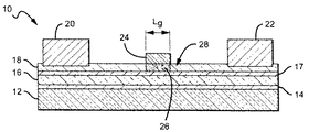
図1は、本発明によるトランジスタ10の一実施形態を示す。トランジスタ10は、III族窒化物ベースのHEMTであることが望ましい。本発明は他の半導体デバイスとともに用いることができること、および、他の材料系も用いることができることが理解されるだろう。III族窒化物とは、窒素と、周期律表のIII族の中の元素との間で形成される半導体化合物のことである。III族の中の元素とは、通常、アルミニウム(Al)、ガリウム(Ga)、およびインジウム(In)である。この用語は、また、AlGaNおよびAlInGaN等の、3元化合物にも用いられる。好ましい一実施形態では、バリア層を形成する材料はAlGaNであり、バッファ層を形成する材料はGaNである。代替的実施形態では、これらの層の材料は、GaN、AlGaN、AlGaAs、または、AlGaInPであってもよいし、他の材料であってもよい。
FIG. 1 illustrates one embodiment of a
HEMT10は、炭化ケイ素、サファイア、スピネット(spinet)、ZnO、ケイ素、窒化ガリウム、窒化アルミニウム、または、III族窒化物材料の成長をサポートすることができる任意の他の材料、または、それらの材料の組み合わせから作ることができる基板12を備える。適切な炭化ケイ素基板は、4Hポリタイプの炭化ケイ素であるが、3C、6H、および15Rポリタイプを含む、他の炭化ケイ素ポリタイプも用いることができる。炭化ケイ素は、他の基板材料と比べて、III族窒化物に整合したより近い結晶格子を持つことができ、その結果、より品質のよいIII族窒化物フィルムを作ることができる。炭化ケイ素はまた、非常に高い熱伝導率を持ち、エミッティングデバイス(emitting device)の熱放散を高めることができる。SiC基板は、ノースカロライナ州ダラム(Durham)在の本件特許出願人より入手可能である。また、SiC基板を製作する方法は、科学文献や特許文献4〜6に開示されている。さらに他の実施形態では、HEMT10は、基板を用いずに形成することもできるし、基板は、エミッタ層を形成した後に取り除かれてもよい。
The
核生成層(nucleation layer)14は、基板12の上に形成されて、HEMT10の中の基板12と次の層との間の格子不整合を低減することができる。核生成層14の厚さは、約1000オングストローム(Å)であるべきだが、他の厚さを用いることもできる。核生成層14は、多くの異なる材料を備えることができるが、適した材料は、AlzGa1-zN(0<=z<=1)である。また、層14は、基板12の上に、有機金属化学気相成長法(MOCVD)、ハイドライド気相成長法(HVPE)、または分子線エピタキシ法(MBE)等の、公知の半導体成長技術を用いて形成することができる。
A
核生成層14の形成は、基板12に用いられる材料に依存する場合がある。例えば、種々の基板の上に核生成層14を形成する方法は、特許文献7および8で教示されている。なお、いずれの文献も、参照により、全ての記載が本明細書に組み込まれる。炭化ケイ素基板の上に核生成層を形成する方法は、特許文献9〜11で開示されている。なお、いずれの文献も、参照により、全て記載が本明細書に組み込まれる。
The formation of the
HEMT10は、核生成層14の上に形成された高抵抗率のバッファ層16をさらに備える。バッファ層16は、III族窒化物材料の、ドープしたまたはドープしない層を備えることができ、AlxGayIn(1-x-y)N(0<=x<=1、0<=y<=1、x+y<=1)等の、III族窒化物材料によって作られることが望ましい。GaN等の、その他の材料もまた、バッファ層16のために用いることができる。この場合、バッファ層の厚さは、約2μmであり、バッファ層の一部にはFeがドープされる。
The
バリア層18はバッファ層16の上に生成され、バッファ層16は、バリア層18と核生成層14との間にサンドイッチされる。バッファ層16と同様に、バリア層18は、III族窒化物材料のドープまたはドープなしの層と、好ましくはAlGaN/GaN材料とを備えることができる。典型的なHEMT構造は、特許文献12〜16に示されている。これらの文献は、参照により、全て記載が本明細書に組み込まれる。この他の窒化物ベースのHEMT構造は、特許文献17および18に示されている。これらの文献は、参照により、全て記載が本明細書に組み込まれる。バッファ層16とバリア層18は、核生成層14を成長させるために用いる方法と同じ方法を用いて形成することができる。デバイス間の電気的なアイソレーションは、活性なHEMTの外側をメサエッチするかまたはイオン注入をするかによって形成することができる。
The
金属ソース電極20と金属ドレイン電極22は、バリア層18にオーム接触を作ることにより形成される。ゲート24は、バリア層18の上でソース電極20とドレイン電極22との間に形成される。当技術分野において知られているように、2次元電子ガス(2DEG)17は、バッファ層16とバリア層18とのヘテロ界面のところに誘起され、形成される。電流は、ゲート24が適当なレベルにバイアスされた場合に、ソース電極20とドレイン電極22との間を、2DEG17を介して流れることができる。ソース電極20およびドレイン電極22の形成は、上述した特許文献および刊行物の中で詳しく説明されている。
The
ソース電極20とドレイン電極22は、種々の材料で作ることができ、その材料は、チタン、アルミニウム、金、またはニッケルの合金を含むが、これらには限定されない。ゲート24も同様に、種々の材料で作ることができ、その材料は、金、ニッケル、ニッケル−クローム、白金、チタン、クローム、チタンとタングステンの合金、または、白金シリサイドを含むが、これらには限定されない。ゲート24は、多くの異なる長さ(Lg)を取ることができ、適したゲート長は、0.1ミクロンから0.2ミクロンの範囲にあるが、他のゲート長も用いることができる。本発明による一実施形態では、好ましいゲート長(Lg)は約0.5ミクロンである。
The
負イオン領域26は、バリア層18の中に含まれるが、他の実施形態では、バッファ層16の中に広がることもできる。負イオン領域は、導入されたまたは埋め込まれた負イオンを中に有する、デバイスのエピタキシャル層の領域であり、周囲の材料と比較して、より多くの負イオンを有する領域を形成する。図示したように、負イオン領域26は、主にゲート24の下にあり、電界を調整するために、希望に応じて、外に広がっている。上述したように、領域26の中の負イオンは、全体的な電界(E)を低減することにより、HEMT10の中の電界を低減する。例えば、負イオンは、バッファ層16とバリア層18との間のAlGaN/GaN界面のところの分極に由来する正の電荷に対して、反対に作用するように配置することができ、それにより、HEMTの正味の電荷を減少させることができる。
The
上記でも述べたように、領域26の中の負イオンは、III族窒化物半導体材料の種々のレベルに浸透することができるフッ素イオンであることが望ましい。上記で示したように、フッ素イオンは、AlGaN/GaNバリア層18の中に浸透するが、他の実施形態では、フッ素イオンは、バッファ層16または核生成層等の下の層の中にも浸透することができる。フッ素イオンは、多くの異なる方法を用いて導入し、層16および層18の中に浸透させることができるが、好ましい方法は、エッチングシステムにおけるフッ素プラズマ処理である。適したエッチングシステムは、リアクティブイオンエッチング(RIE)処理または誘導結合プラズマエッチング(ICP)処理を用いた、フッ素ベースのドライエッチを含む。その他の実施形態では、イオン注入処理を用いることができる。種々の異なる材料を、エッチング処理に用いることができる。これらは、CF4、SF6、または、CHF3のプラズマガス化学処理を含むが、それに限定はされない。好ましい実施形態においては、エッチングの方法は、エッチングを行っている間にAlGaN/GaN材料に損傷を与えてはならず、AlGaN/GaNに浸透するフッ素イオンのソースを設けなければならない。
As mentioned above, the negative ions in
希望する深さの浸透を達成するために必要な時間は、いくつかの異なる要因に依存する。フッ素イオンがバリア層18の中に注入されて、バリア層18またはバッファ層16の中に広がる速度は、一般に、エッチング処理に用いる電圧(電力)レベル、エッチング処理を行っている間のガスの流量、ガス濃度、および、表面に対してエッチを行う時間に依存する。電圧レベル、ガス濃度、およびガスの流量が高ければ、浸透が希望のレベルに達するまでの時間は短くなるであろう。フッ素イオンの浸透が希望する区画だけに起きて、希望する負イオン領域が形成されるように、マスクを含むこができる。
The time required to achieve the desired depth of penetration depends on several different factors. The rate at which fluorine ions are implanted into the
種々の負イオン領域の深さと幅とを有する負イオンプロファイルを得るために、エッチング処理はカスタマイズすることができる。また、領域の異なる部分は、異なるイオン濃度、または異なる深さにすることができる。限定的でない例として、公知の複数のマスキング技術を含む多くの異なる方法が、このプロファイルを形成するために用いることができる。AlGaN/GaNと異なる材料系で作られるHEMTでは、その材料系に損傷を与えない種々のエッチング処理を、負イオンを導入するために用いることができる。 The etching process can be customized to obtain negative ion profiles having various negative ion region depths and widths. Also, different portions of the region can have different ion concentrations or different depths. By way of non-limiting example, many different methods can be used to form this profile, including known masking techniques. In a HEMT made of a material system different from AlGaN / GaN, various etching processes that do not damage the material system can be used to introduce negative ions.
フッ素イオンは、トランジスタの電界の高い他の領域に負イオン領域を設けるために、エピタキシャル層の他の区画にさらに導入することができる。電界の高い領域の別の例は、メサアイソレーションの端の部分である。負イオン領域を設けて、ゲート金属がメサの端を横切る場所における漏れ電流と、ゲート金属パッドの下の漏れ電流とを低減するように、メサアイソレーション処理のフォロウアップ(follow-up)ステップとして、フッ素処理を用いることができる。 Fluorine ions can be further introduced into other sections of the epitaxial layer to provide negative ion regions in other regions of the transistor where the electric field is high. Another example of a region with a high electric field is the end portion of mesa isolation. As a follow-up step in the mesa isolation process to provide a negative ion region to reduce leakage current where the gate metal crosses the edge of the mesa and under the gate metal pad Fluorine treatment can be used.
HEMT10の動作時に、電界は、ゲートからドレインまでの領域28と、その周囲に広がって行く。負イオン領域26は、この電界を打ち消して低減するように配置され、その結果、降伏電圧が上昇してトラップが減少する。電界の低減は、漏れ電流の低減および信頼度の向上等の、その他の利益ももたらすことができる。
During the operation of the
本発明は、フィールドプレート等の、電界を調整するための他の構造/特徴を有するデバイスの中で用いることができる。図2は、本発明によるHEMT40の別の実施形態を示す。HEMT40も、基板12、AlGaN/GaN核生成層14、AlGaN/GaNバッファ層16、AlGaN/GaNバリア層18、ソース電極20、ドレイン電極22、および、ゲート24を有する。第1の非導電性スペーサ層42が、ゲート24とソース電極20との間およびゲート24とドレイン電極22との間のバリア層18の表面を覆って形成される。第1のスペーサ層42は、誘電体層、または、複数の誘電体層の組み合わせを備えることができる。SiN、SiO2、Si、Ge、MgOx、MgNx、ZnO、SiNx、SiOx、これらの混合または順番に重ねた層等の、種々の誘電体材料が使用可能である。スペーサ層は、多くの異なる厚さであってよいが、適した厚さの範囲は、約0.05ミクロンから2ミクロンである。
The present invention can be used in devices having other structures / features for adjusting the electric field, such as field plates. FIG. 2 shows another embodiment of a
デバイスのメタライゼーション(metallization)の前にスペーサ層42が形成される場合には、スペーサ層はまた、Al、Ga、または、Inの合金等の、III族元素を有するIII族窒化物材料等の、エピタキシャル材料を備えることができるが、適したスペーサ層材料は、AlxGa1-xN(0≦x≦1)である。バリア層18をエピタキシャル成長させた後に、同じエピタキシャル成長の方法を用いて、第1のスペーサ層42を成長させることができる。適した誘電体スペーサ層はまた、バリア層のエピタキシャル成長の後に、同じエピタキシャル成長の方法を用いて成長させることができる。
If the
次いで、第1のスペーサ層42がエッチングされ、ゲート24、ソース電極20、およびドレイン電極22は、2DEG17と電気的に接触するように適切に形成することができる。フッ素(負)イオンをバリア層18の中に注入し、希望に応じて、バッファ層16の中に広げることができるのは、このエッチング処理の間である。ゲート線は、典型的に、スペーサ層の中で確定され、ゲートのための空間は、エッチングにより空けられる。典型的には、スペーサ層42は、フッ素ベースのRIEを用いてエッチングされる。スペーサ層42のエッチングに続いて、バリア層18は、さらにフッ素暴露処理を行い、バリア層18のAlGaN/GaNの中に、希望するフッ素イオンを浸透させることができる。他の実施形態では、スペーサ層42の堆積(deposition)およびエッチングの前に、フッ素イオンをバリア層の中に注入することができる。フッ素イオンは負電荷を帯びており、AlGaN/GaN材料系の中の正の分極電荷を打ち消すドープ剤として働く。
Then, the
第1のフィールドプレート44は、スペーサ層42の上に形成され、ゲート24からドレイン電極22の方に向かって広がる。フィールドプレートはまた、ソース電極20の方に向かって広がる部分を有することができる。スペーサ層42は、第1のフィールドプレート44と下の層との間のアイソレーションを与えるように配置される。図に示すように、フィールドプレート44は、ゲート24に集積されているが、他の実施形態ではゲート24から分離されていてもよく、ゲート24またはソース電極20と電気的に結合する。
The
フィールドプレート44は、ゲート24の端からバリア層の上に種々の距離Lfにわたり広がることができ、適した距離の範囲は、0.1ミクロンから1.0ミクロンであるが、異なる距離であってもよい。フィールドプレート44は、多くの異なる導電性材料を備えてよいが、適した材料は、標準的なメタライゼーションの方法を用いた金属堆積である。このフィールドプレート配置は、デバイスの中のピーク電界を低減し、その結果、降伏電圧の上昇、漏れ電流の低減、および、信頼度の向上を得ることができる。ソースに結合したフィールドプレートのシールド効果はまた、Cgdを減少させることができ、それにより、入力−出力のアイソレーションを増すことができる。このフィールドプレートの配置は、上述したように、負イオン領域26と一緒に用いることができ、デバイスの動作をさらに向上させる。
The
図3は、本発明によるHEMT50の別の実施形態を示す。HEMT50も、基板12、核生成層14、バッファ層16、バリア層18、ソース電極20、ドレイン電極22、および、ゲート24を有する。スペーサ層42は、バリア層18の上で、ゲート24とソース電極20との間、およびゲート24とドレイン電極22との間に含まれる。スペーサ層42は、ゲート24に対する開口を設け、負イオンを注入するために、上述したようにエッチングされる。フィールドプレート44は、スペーサ層42の上に形成され、ゲート24に集積される。他の実施形態では、フィールドプレート44は、ゲート24から分離された形で、ゲート24またはソース電極20と電気的に結合されてもよい。
FIG. 3 shows another embodiment of a
HEMT50は、スペーサ層42と同じ材料で作ることができる、第2の非導電性スペーサ層52をさらに備える。第2のフィールドプレート54は、スペーサ層42の上にあって、第1のフィールドプレート44およびゲート24と重なっている。しかし、他の実施形態では、フィールドプレート44とだけ重なっていてもよいし、またはどちらとも重なっていなくてもよい。第2のフィールドプレート54は、典型的には、ソース電極20と電気的に接続される。上記の実施形態は、マイクロ波周波数およびミリメートル波周波数において電力を向上させたワイドバンドギャップトランジスタを与える。複数個のフィールドプレートを有するトランジスタは、入力と出力との間の高いアイソレーションによって、高利得、高電力、およびより安定的な動作を同時に実現する。
The
複数のフィールドプレートの配置は、上述した方法を用いてバリア層18の中に注入されたフッ素イオンを備えることが望ましい、負イオン領域56と一緒に用いることもできる。図示したように、領域56は、バッファ層16の中に広がることができる、異なる厚さの部分を備えることができる。第1の領域58は、主にゲート24の下にあり、バッファ層16の中には広がらない。部分58は、典型的には、スペーサ層42のエッチング時に形成される。第2の部分60は、おもに、第1のフィールドプレート44の下方にあり、バッファ層16の中に広がる。第3の部分62は、おもに、第2のフィールドプレート54の一部の下方にあり、ドレイン22の方に向かって広がっている。第2の部分60と第3の部分62は、典型的には、スペーサ層42の堆積を行う前に形成される。この調整された負イオン領域56は、フィールドプレート44およびフィールドプレート54と一緒に働き、電界を低減してデバイス動作を向上させる。
A plurality of field plate arrangements can also be used with the
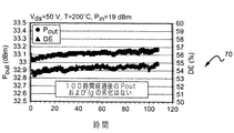
図4は、図2に示して上述したHEMT10と同様な、幅246μmのデバイスの動作を示すグラフ70である。デバイスは、ドレインバイアス50V、ベース電極温度200℃、連続出力電力8.3W/mmの100時間動作の後で、何も劣化を示さない。
FIG. 4 is a
図5は、2つのデバイスの動作を示すグラフ80であり、一方は低いフッ素ドーズ量を有し、もう一方は高いドーズ量を有する。どちらのデバイスも高温高電界ストレス試験を行い、高フッ素デバイスの方が低ドーズデバイスと比較して、より低いゲート漏れ電流を示した。これらの結果は、フッ素イオンのレベルが全体的な電界を低減して、それによりデバイス動作が改善されるという事実をサポートしている。
FIG. 5 is a
いくつかの半導体材料では、高い温度、または高い電界のもとでは、負イオンが、半導体材料の中でマイグレーションを起こす(migrate)、または、材料から散逸(dissipate)することがある。高温下でのマイグレーション/散逸(dissipation)を減少させるため、負イオンプロファイルを有する半導体デバイスは、熱処理を行って、注入されたイオンを安定化させることができる。多くの異なる熱処理温度と熱処理時間とが可能であるが、適した熱処理温度の範囲は、200°から1000°である。高電界下でのマイグレーション/散逸を減少させるために、負イオンプロファイルを有する半導体デバイスには、「バーンイン(burn in)」処理として知られる、デバイスにある期間バイアスをかける処理を施すことができる。 In some semiconductor materials, under high temperatures or high electric fields, negative ions can migrate or dissipate from the semiconductor material. In order to reduce migration / dissipation at high temperatures, a semiconductor device having a negative ion profile can be heat treated to stabilize implanted ions. Many different heat treatment temperatures and heat treatment times are possible, but a suitable heat treatment temperature range is 200 ° to 1000 °. In order to reduce migration / dissipation under high electric fields, semiconductor devices having a negative ion profile can be subjected to a process of biasing the device for a period of time, known as a “burn in” process.
図6は、本発明による半導体デバイスを製造するための、特に、III族窒化物HEMTを製造するための、本発明による方法90の一実施形態である。方法90は、一連のステップとして示されているが、本発明によれば、方法の中で、異なるステップが異なる順序で行われてもよいことが理解されるだろう。
FIG. 6 is one embodiment of a
ステップ92において、基板が設けられる。基板は、多くの異なる材料によって作られたものでよいが、図1に示した基板12のために列挙され、上記で詳しく説明した任意の材料が適した材料である。ステップ94において、MOCVD、HVPE、または、MBE等による公知の半導体のいずれかを用いて、基板の上にエピタキシャル層を成長させる。HEMTについては、エピタキシャル層は、少なくともバッファとバリア層とを含み、2つの層の間のヘテロ界面の中に2DEGを有する、III族窒化物層であることが望ましい。
In
ステップ96において、負イオンがエピタキシャル層の中に導入され、負イオンは浸透して負イオン領域を形成することができる。負イオンの導入には多くの異なる方法を用いることができるが、上述したように、好ましい方法は、リアクティブイオンエッチング(RIE)か、誘導結合プラズマエッチング(ICP)処理を用いた、フッ素ベースのドライエッチングである。上述したように、エッチング処理には種々の材料を用いることができ、エッチング処理により、エピタキシャル層は本質的に無損傷でなければならない。負イオン領域は、HEMTの完成品の動作時電界を打ち消す位置に形成されるべきである。
In
負イオン領域が、ある特定の深さまたは濃度プロファイルを有する実施形態に対しては、さらに付加的な負イオン導入のステップを実行することができる。当技術分野において公知のステップを用いた公知のマスキング方法を用いることができる。ステップ98において、ソース電極(コンタクト)とドレイン電極(コンタクト)は、バリア層とオーミック接触を作るように形成され、ゲート24が、バリア層の上でソース電極とドレイン電極との間に形成される。それぞれは、上述した材料によって作ることができ、公知の処理を用いて形成される。他の実施形態においては、ソースコンタクトおよびドレインコンタクトは、そのどちらか、またはいずれも、負イオン領域の形成の前に形成することができる。ゲートは、負イオン領域を形成した後に、形成することができる。
For embodiments where the negative ion region has a certain depth or concentration profile, additional negative ion introduction steps can be performed. Any known masking method using steps known in the art can be used. In
本発明による方法は、付加的なデバイス処理のステップ100を含むことができると理解されるだろう。たとえば、上述したように、負イオン領域を安定化させるための、熱処理またはバーンインのステップが含まれてもよい。上記で説明し、図2および図3に示されているフィールドプレートデバイスを形成するために、デバイスの上に1つまたはそれ以上のフィールドプレートを形成するための付加的なステップが、さらに実行されてもよい。
It will be appreciated that the method according to the invention may include an additional
本発明が、いくつかの好ましい構成を参照して詳しく説明されたが、他の形態も可能である。負イオン領域は、本発明による多くの異なるデバイスの中で用いること、多くの異なる形状をもつこと、および、多くの異なる位置に置かれることが可能である。従って、本発明の趣旨と範囲は、上述した形態に限定されるべきではない。 Although the invention has been described in detail with reference to certain preferred configurations, other forms are possible. The negative ion region can be used in many different devices according to the present invention, can have many different shapes, and can be placed in many different locations. Therefore, the spirit and scope of the present invention should not be limited to the above-described embodiments.
Claims (12)
前記バッファ層の上のバリア層と、
前記バッファ層と前記バリア層との界面における2次元電子ガス(2DEG)と、
ゲート、ソースコンタクトおよびドレインコンタクトと、
前記バリア層の中の負イオン領域と
を備え、
前記ソースコンタクトと前記ドレインコンタクトの間に前記ゲートがあり、
前記負イオン領域は、主として前記ゲートの下方において存在するとともに、前記ゲートの端を超えて存在するように、前記バッファ層の中に広がっていることを特徴とする高電子移動度トランジスタ(HEMT)。 A buffer layer,
A barrier layer on the buffer layer;
A two-dimensional electron gas (2DEG) at the interface between the buffer layer and the barrier layer;
A gate, a source contact and a drain contact;
A negative ion region in the barrier layer,
The gate is between the source contact and the drain contact;
The high ion mobility transistor (HEMT) is characterized in that the negative ion region exists mainly below the gate and extends beyond the edge of the gate so as to exist in the buffer layer. .
前記負イオン領域は、フッ素イオンを備えることを特徴とする請求項1に記載のHEMT。 The buffer layer and the barrier layer are made of a III-nitride material;
The HEMT according to claim 1, wherein the negative ion region includes fluorine ions.
動作時電(E)界がかかる複数の活性半導体層であって、バッファ層の上のバリア層を含む複数の活性半導体層と、
少なくとも前記バリア層の中に存在する負イオン領域であって、主としてゲートの下方において存在するとともに、前記ゲートの端を超えて存在する負イオン領域と
を備えることを特徴とする半導体デバイス。 A semiconductor-based device,
A plurality of active semiconductor layers to which an operating electric field (E) is applied, and a plurality of active semiconductor layers including a barrier layer on the buffer layer ;
A negative ions area present in at least the barrier layer, with predominantly present below the gate, a semiconductor device characterized by comprising a negative ion region present beyond the end of the gate.
前記バッファ層の上の、III族窒化物ベースのバリア層と、
前記バッファ層と前記バリア層とのヘテロ界面における2次元電子ガス(2DEG)と、
前記バリア層の上のソースコンタクトおよびドレインコンタクトと、
前記ソースコンタクトと前記ドレインコンタクトとの間の前記バリア層の上のゲートと、
前記バリア層の下に配置されており、前記バリア層の中に広がっており、かつ前記ゲートの端から前記ドレインへ広がっている、HEMTの中のフッ素負イオン領域と
を備えることを特徴とする高電子移動度トランジスタ(HEMT)。 A III-nitride based buffer layer;
A III-nitride based barrier layer on the buffer layer;
A two-dimensional electron gas (2DEG) at the heterointerface between the buffer layer and the barrier layer;
A source contact and a drain contact on the barrier layer;
A gate over the barrier layer between the source contact and the drain contact;
A fluorine negative ion region in the HEMT, disposed under the barrier layer, extending into the barrier layer, and extending from an end of the gate to the drain. High electron mobility transistor (HEMT).
基板を設けるステップと、
前記基板の上に、バッファ層とバリア層とを含むエピタキシャル層を成長させるステップと、
前記エピタキシャル層の中に負イオンを導入し、前記バッファ層及び前記バリア層の中に負イオン領域を形成するステップと、
前記バリア層上及び前記負イオン領域の少なくとも一部分の上にゲートを形成するステップであって、前記負イオン領域が、少なくとも部分的に、前記ゲートの下方において及び前記ゲートの端を超えて存在するステップと
を備えることを特徴とする方法。 A method of manufacturing a semiconductor device, comprising:
Providing a substrate;
Growing an epitaxial layer including a buffer layer and a barrier layer on the substrate;
Introducing negative ions into the epitaxial layer to form negative ion regions in the buffer layer and the barrier layer ;
Forming a gate over the barrier layer and over at least a portion of the negative ion region, the negative ion region being at least partially below the gate and beyond the edge of the gate. A method comprising the steps of:
前記負イオンは、フッ素イオンを備えることを特徴とする請求項8に記載の方法。 The epitaxial layer is made of a group III nitride material;
The method of claim 8, wherein the negative ions comprise fluorine ions.
Applications Claiming Priority (3)
| Application Number | Priority Date | Filing Date | Title |
|---|---|---|---|
| US71505705P | 2005-09-07 | 2005-09-07 | |
| US60/715,057 | 2005-09-07 | ||
| PCT/US2006/026405 WO2008027027A2 (en) | 2005-09-07 | 2006-07-07 | Transistor with fluorine treatment |
Publications (2)
| Publication Number | Publication Date |
|---|---|
| JP2009507396A JP2009507396A (en) | 2009-02-19 |
| JP5501618B2 true JP5501618B2 (en) | 2014-05-28 |
Family
ID=39136403
Family Applications (1)
| Application Number | Title | Priority Date | Filing Date |
|---|---|---|---|
| JP2008532215A Active JP5501618B2 (en) | 2005-09-07 | 2006-07-07 | High electron transfer transistor (HEMT), semiconductor device and manufacturing method thereof |
Country Status (5)
| Country | Link |
|---|---|
| US (3) | US7638818B2 (en) |
| EP (3) | EP2312634B1 (en) |
| JP (1) | JP5501618B2 (en) |
| TW (1) | TW200715570A (en) |
| WO (1) | WO2008027027A2 (en) |
Cited By (1)
| Publication number | Priority date | Publication date | Assignee | Title |
|---|---|---|---|---|
| WO2022120072A1 (en) * | 2020-12-02 | 2022-06-09 | Analog Devices, Inc. | Compound semiconductor devices with a conductive component to control electrical characteristics |
Families Citing this family (168)
| Publication number | Priority date | Publication date | Assignee | Title |
|---|---|---|---|---|
| WO2003032397A2 (en) | 2001-07-24 | 2003-04-17 | Cree, Inc. | INSULTING GATE AlGaN/GaN HEMT |
| US7417266B1 (en) | 2004-06-10 | 2008-08-26 | Qspeed Semiconductor Inc. | MOSFET having a JFET embedded as a body diode |
| US7863648B2 (en) * | 2005-06-10 | 2011-01-04 | Nec Corporation | Field effect transistor |
| US8183595B2 (en) * | 2005-07-29 | 2012-05-22 | International Rectifier Corporation | Normally off III-nitride semiconductor device having a programmable gate |
| JP5501618B2 (en) | 2005-09-07 | 2014-05-28 | クリー インコーポレイテッド | High electron transfer transistor (HEMT), semiconductor device and manufacturing method thereof |
| US8114717B2 (en) * | 2005-11-15 | 2012-02-14 | The Regents Of The University Of California | Methods to shape the electric field in electron devices, passivate dislocations and point defects, and enhance the luminescence efficiency of optical devices |
| US7932539B2 (en) * | 2005-11-29 | 2011-04-26 | The Hong Kong University Of Science And Technology | Enhancement-mode III-N devices, circuits, and methods |
| US7972915B2 (en) * | 2005-11-29 | 2011-07-05 | The Hong Kong University Of Science And Technology | Monolithic integration of enhancement- and depletion-mode AlGaN/GaN HFETs |
| US8044432B2 (en) * | 2005-11-29 | 2011-10-25 | The Hong Kong University Of Science And Technology | Low density drain HEMTs |
| JP5307973B2 (en) * | 2006-02-24 | 2013-10-02 | セミコンダクター・コンポーネンツ・インダストリーズ・リミテッド・ライアビリティ・カンパニー | Semiconductor device |
| JP4989085B2 (en) * | 2006-02-24 | 2012-08-01 | オンセミコンダクター・トレーディング・リミテッド | Semiconductor device and manufacturing method thereof |
| JP5065616B2 (en) * | 2006-04-21 | 2012-11-07 | 株式会社東芝 | Nitride semiconductor device |
| US7692263B2 (en) | 2006-11-21 | 2010-04-06 | Cree, Inc. | High voltage GaN transistors |
| EP2135286B1 (en) * | 2007-02-22 | 2015-09-23 | Forschungsverbund Berlin E.V. | Semiconductor component with field plate structure and method for producing the same |
| US9147644B2 (en) * | 2008-02-26 | 2015-09-29 | International Rectifier Corporation | Semiconductor device and passive component integration in a semiconductor package |
| US8786072B2 (en) * | 2007-02-27 | 2014-07-22 | International Rectifier Corporation | Semiconductor package |
| US20080203433A1 (en) * | 2007-02-27 | 2008-08-28 | Sanken Electric Co., Ltd. | High electron mobility transistor and method of forming the same |
| US7939853B2 (en) * | 2007-03-20 | 2011-05-10 | Power Integrations, Inc. | Termination and contact structures for a high voltage GaN-based heterojunction transistor |
| JP4691060B2 (en) * | 2007-03-23 | 2011-06-01 | 古河電気工業株式会社 | GaN-based semiconductor devices |
| US8212290B2 (en) † | 2007-03-23 | 2012-07-03 | Cree, Inc. | High temperature performance capable gallium nitride transistor |
| JP2008277604A (en) * | 2007-05-01 | 2008-11-13 | Oki Electric Ind Co Ltd | Field-effect transistor |
| JP5306341B2 (en) * | 2007-07-04 | 2013-10-02 | コーニンクレッカ フィリップス エヌ ヴェ | Method for forming a patterned layer on a substrate |
| US8461626B2 (en) * | 2007-07-09 | 2013-06-11 | Freescale Semiconductor, Inc. | Hetero-structure field effect transistor, integrated circuit including a hetero-structure field effect transistor and method for manufacturing a hetero-structure field effect transistor |
| US8502323B2 (en) * | 2007-08-03 | 2013-08-06 | The Hong Kong University Of Science And Technology | Reliable normally-off III-nitride active device structures, and related methods and systems |
| WO2009038809A1 (en) * | 2007-09-20 | 2009-03-26 | International Rectifier Corporation | Enhancement mode iii-nitride semiconductor device with reduced electric field between the gate and the drain |
| FR2924271B1 (en) * | 2007-11-27 | 2010-09-03 | Picogiga Internat | CONTROLLED ELECTRIC FIELD ELECTRONIC DEVICE |
| JP5671100B2 (en) * | 2008-02-13 | 2015-02-18 | 株式会社東芝 | Semiconductor device |
| JP5416399B2 (en) * | 2008-02-13 | 2014-02-12 | 株式会社東芝 | Semiconductor device |
| US8497527B2 (en) * | 2008-03-12 | 2013-07-30 | Sensor Electronic Technology, Inc. | Device having active region with lower electron concentration |
| US8076699B2 (en) * | 2008-04-02 | 2011-12-13 | The Hong Kong Univ. Of Science And Technology | Integrated HEMT and lateral field-effect rectifier combinations, methods, and systems |
| US8519438B2 (en) | 2008-04-23 | 2013-08-27 | Transphorm Inc. | Enhancement mode III-N HEMTs |
| US8871024B2 (en) * | 2008-06-05 | 2014-10-28 | Soraa, Inc. | High pressure apparatus and method for nitride crystal growth |
| US9157167B1 (en) | 2008-06-05 | 2015-10-13 | Soraa, Inc. | High pressure apparatus and method for nitride crystal growth |
| US8097081B2 (en) | 2008-06-05 | 2012-01-17 | Soraa, Inc. | High pressure apparatus and method for nitride crystal growth |
| US20090301388A1 (en) * | 2008-06-05 | 2009-12-10 | Soraa Inc. | Capsule for high pressure processing and method of use for supercritical fluids |
| WO2011044554A1 (en) | 2009-10-09 | 2011-04-14 | Soraa, Inc. | Method for synthesis of high quality large area bulk gallium based crystals |
| US7985986B2 (en) * | 2008-07-31 | 2011-07-26 | Cree, Inc. | Normally-off semiconductor devices |
| US8979999B2 (en) | 2008-08-07 | 2015-03-17 | Soraa, Inc. | Process for large-scale ammonothermal manufacturing of gallium nitride boules |
| US8430958B2 (en) * | 2008-08-07 | 2013-04-30 | Soraa, Inc. | Apparatus and method for seed crystal utilization in large-scale manufacturing of gallium nitride |
| US10036099B2 (en) | 2008-08-07 | 2018-07-31 | Slt Technologies, Inc. | Process for large-scale ammonothermal manufacturing of gallium nitride boules |
| US8021481B2 (en) | 2008-08-07 | 2011-09-20 | Soraa, Inc. | Process and apparatus for large-scale manufacturing of bulk monocrystalline gallium-containing nitride |
| US7976630B2 (en) | 2008-09-11 | 2011-07-12 | Soraa, Inc. | Large-area seed for ammonothermal growth of bulk gallium nitride and method of manufacture |
| US8289065B2 (en) * | 2008-09-23 | 2012-10-16 | Transphorm Inc. | Inductive load power switching circuits |
| US8354679B1 (en) | 2008-10-02 | 2013-01-15 | Soraa, Inc. | Microcavity light emitting diode method of manufacture |
| US20100295088A1 (en) * | 2008-10-02 | 2010-11-25 | Soraa, Inc. | Textured-surface light emitting diode and method of manufacture |
| US20100084687A1 (en) * | 2008-10-03 | 2010-04-08 | The Hong Kong University Of Science And Technology | Aluminum gallium nitride/gallium nitride high electron mobility transistors |
| US8455894B1 (en) | 2008-10-17 | 2013-06-04 | Soraa, Inc. | Photonic-crystal light emitting diode and method of manufacture |
| US7898004B2 (en) | 2008-12-10 | 2011-03-01 | Transphorm Inc. | Semiconductor heterostructure diodes |
| US8987156B2 (en) | 2008-12-12 | 2015-03-24 | Soraa, Inc. | Polycrystalline group III metal nitride with getter and method of making |
| US8461071B2 (en) * | 2008-12-12 | 2013-06-11 | Soraa, Inc. | Polycrystalline group III metal nitride with getter and method of making |
| US8878230B2 (en) * | 2010-03-11 | 2014-11-04 | Soraa, Inc. | Semi-insulating group III metal nitride and method of manufacture |
| US9543392B1 (en) | 2008-12-12 | 2017-01-10 | Soraa, Inc. | Transparent group III metal nitride and method of manufacture |
| USRE47114E1 (en) | 2008-12-12 | 2018-11-06 | Slt Technologies, Inc. | Polycrystalline group III metal nitride with getter and method of making |
| US20110100291A1 (en) * | 2009-01-29 | 2011-05-05 | Soraa, Inc. | Plant and method for large-scale ammonothermal manufacturing of gallium nitride boules |
| JP2010186943A (en) * | 2009-02-13 | 2010-08-26 | Sharp Corp | Nitride semiconductor device |
| US8247886B1 (en) | 2009-03-09 | 2012-08-21 | Soraa, Inc. | Polarization direction of optical devices using selected spatial configurations |
| US8299473B1 (en) | 2009-04-07 | 2012-10-30 | Soraa, Inc. | Polarized white light devices using non-polar or semipolar gallium containing materials and transparent phosphors |
| US8008977B2 (en) * | 2009-04-14 | 2011-08-30 | Triquint Semiconductor, Inc. | Field-plated transistor including feedback resistor |
| US8754496B2 (en) * | 2009-04-14 | 2014-06-17 | Triquint Semiconductor, Inc. | Field effect transistor having a plurality of field plates |
| WO2010122628A1 (en) * | 2009-04-20 | 2010-10-28 | 富士通株式会社 | Compound semiconductor device and method for manufacturing the same |
| US8742459B2 (en) | 2009-05-14 | 2014-06-03 | Transphorm Inc. | High voltage III-nitride semiconductor devices |
| US8791499B1 (en) | 2009-05-27 | 2014-07-29 | Soraa, Inc. | GaN containing optical devices and method with ESD stability |
| US8728884B1 (en) | 2009-07-28 | 2014-05-20 | Hrl Laboratories, Llc | Enhancement mode normally-off gallium nitride heterostructure field effect transistor |
| US9000466B1 (en) | 2010-08-23 | 2015-04-07 | Soraa, Inc. | Methods and devices for light extraction from a group III-nitride volumetric LED using surface and sidewall roughening |
| US8390000B2 (en) | 2009-08-28 | 2013-03-05 | Transphorm Inc. | Semiconductor devices with field plates |
| US9293644B2 (en) | 2009-09-18 | 2016-03-22 | Soraa, Inc. | Power light emitting diode and method with uniform current density operation |
| US9583678B2 (en) | 2009-09-18 | 2017-02-28 | Soraa, Inc. | High-performance LED fabrication |
| CN102630349B (en) | 2009-09-18 | 2017-06-13 | 天空公司 | Method power led and using current density operation |
| US8933644B2 (en) | 2009-09-18 | 2015-01-13 | Soraa, Inc. | LED lamps with improved quality of light |
| KR20110032845A (en) * | 2009-09-24 | 2011-03-30 | 삼성전자주식회사 | Power electronic device and method of manufacturing the same |
| US8435347B2 (en) | 2009-09-29 | 2013-05-07 | Soraa, Inc. | High pressure apparatus with stackable rings |
| JP5037594B2 (en) * | 2009-12-08 | 2012-09-26 | シャープ株式会社 | Field effect transistor |
| US8389977B2 (en) | 2009-12-10 | 2013-03-05 | Transphorm Inc. | Reverse side engineered III-nitride devices |
| US8740413B1 (en) | 2010-02-03 | 2014-06-03 | Soraa, Inc. | System and method for providing color light sources in proximity to predetermined wavelength conversion structures |
| US8905588B2 (en) | 2010-02-03 | 2014-12-09 | Sorra, Inc. | System and method for providing color light sources in proximity to predetermined wavelength conversion structures |
| US20110186874A1 (en) * | 2010-02-03 | 2011-08-04 | Soraa, Inc. | White Light Apparatus and Method |
| US10147850B1 (en) | 2010-02-03 | 2018-12-04 | Soraa, Inc. | System and method for providing color light sources in proximity to predetermined wavelength conversion structures |
| US9450143B2 (en) | 2010-06-18 | 2016-09-20 | Soraa, Inc. | Gallium and nitrogen containing triangular or diamond-shaped configuration for optical devices |
| US9564320B2 (en) | 2010-06-18 | 2017-02-07 | Soraa, Inc. | Large area nitride crystal and method for making it |
| US20120007102A1 (en) * | 2010-07-08 | 2012-01-12 | Soraa, Inc. | High Voltage Device and Method for Optical Devices |
| JP5655424B2 (en) * | 2010-08-09 | 2015-01-21 | サンケン電気株式会社 | Compound semiconductor device |
| US8729559B2 (en) | 2010-10-13 | 2014-05-20 | Soraa, Inc. | Method of making bulk InGaN substrates and devices thereon |
| TWI421947B (en) * | 2010-11-12 | 2014-01-01 | Univ Nat Chiao Tung | A method for fabricating a gan thin film transistor |
| JP5707903B2 (en) * | 2010-12-02 | 2015-04-30 | 富士通株式会社 | Compound semiconductor device and manufacturing method thereof |
| JP5786323B2 (en) * | 2010-12-03 | 2015-09-30 | 富士通株式会社 | Method for manufacturing compound semiconductor device |
| US8742460B2 (en) | 2010-12-15 | 2014-06-03 | Transphorm Inc. | Transistors with isolation regions |
| US8786053B2 (en) | 2011-01-24 | 2014-07-22 | Soraa, Inc. | Gallium-nitride-on-handle substrate materials and devices and method of manufacture |
| US8643062B2 (en) | 2011-02-02 | 2014-02-04 | Transphorm Inc. | III-N device structures and methods |
| JP5857415B2 (en) * | 2011-02-24 | 2016-02-10 | 富士通株式会社 | Manufacturing method of semiconductor device |
| US8772842B2 (en) | 2011-03-04 | 2014-07-08 | Transphorm, Inc. | Semiconductor diodes with low reverse bias currents |
| US8716141B2 (en) | 2011-03-04 | 2014-05-06 | Transphorm Inc. | Electrode configurations for semiconductor devices |
| US9631620B2 (en) * | 2011-03-11 | 2017-04-25 | Johnson Controls Technology Company | Stationary volume ratio adjustment mechanism |
| CN102184943A (en) * | 2011-04-18 | 2011-09-14 | 电子科技大学 | Enhanced AlGaN/GaN HEMT (High Electron Mobility Transistor) device and manufacturing method thereof |
| US8492185B1 (en) | 2011-07-14 | 2013-07-23 | Soraa, Inc. | Large area nonpolar or semipolar gallium and nitrogen containing substrate and resulting devices |
| US8686431B2 (en) | 2011-08-22 | 2014-04-01 | Soraa, Inc. | Gallium and nitrogen containing trilateral configuration for optical devices |
| US8901604B2 (en) | 2011-09-06 | 2014-12-02 | Transphorm Inc. | Semiconductor devices with guard rings |
| US9257547B2 (en) | 2011-09-13 | 2016-02-09 | Transphorm Inc. | III-N device structures having a non-insulating substrate |
| JP5782947B2 (en) * | 2011-09-15 | 2015-09-24 | 富士通株式会社 | Semiconductor device and manufacturing method thereof, power supply device, and high-frequency amplifier |
| JP5765171B2 (en) * | 2011-09-29 | 2015-08-19 | 富士通株式会社 | Method for manufacturing compound semiconductor device |
| US8598937B2 (en) | 2011-10-07 | 2013-12-03 | Transphorm Inc. | High power semiconductor electronic components with increased reliability |
| US9694158B2 (en) | 2011-10-21 | 2017-07-04 | Ahmad Mohamad Slim | Torque for incrementally advancing a catheter during right heart catheterization |
| US10029955B1 (en) | 2011-10-24 | 2018-07-24 | Slt Technologies, Inc. | Capsule for high pressure, high temperature processing of materials and methods of use |
| US20130105817A1 (en) | 2011-10-26 | 2013-05-02 | Triquint Semiconductor, Inc. | High electron mobility transistor structure and method |
| US8912025B2 (en) | 2011-11-23 | 2014-12-16 | Soraa, Inc. | Method for manufacture of bright GaN LEDs using a selective removal process |
| US8633094B2 (en) | 2011-12-01 | 2014-01-21 | Power Integrations, Inc. | GaN high voltage HFET with passivation plus gate dielectric multilayer structure |
| US8940620B2 (en) | 2011-12-15 | 2015-01-27 | Power Integrations, Inc. | Composite wafer for fabrication of semiconductor devices |
| US8482104B2 (en) | 2012-01-09 | 2013-07-09 | Soraa, Inc. | Method for growth of indium-containing nitride films |
| KR101869045B1 (en) * | 2012-01-11 | 2018-06-19 | 삼성전자 주식회사 | High electron mobility transistor and method of manufacturing the same |
| US9165766B2 (en) | 2012-02-03 | 2015-10-20 | Transphorm Inc. | Buffer layer structures suited for III-nitride devices with foreign substrates |
| EP2823515A4 (en) | 2012-03-06 | 2015-08-19 | Soraa Inc | Light emitting diodes with low refractive index material layers to reduce light guiding effects |
| JP5701805B2 (en) * | 2012-03-28 | 2015-04-15 | 株式会社東芝 | Manufacturing method of nitride semiconductor Schottky diode |
| JP5995309B2 (en) * | 2012-03-28 | 2016-09-21 | 住友電工デバイス・イノベーション株式会社 | Semiconductor device and manufacturing method thereof |
| JP5715588B2 (en) * | 2012-03-28 | 2015-05-07 | 株式会社東芝 | Semiconductor device and manufacturing method thereof |
| US9093366B2 (en) | 2012-04-09 | 2015-07-28 | Transphorm Inc. | N-polar III-nitride transistors |
| US20130328061A1 (en) * | 2012-06-07 | 2013-12-12 | Hrl Laboratories, Llc. | Normally-off gallium nitride transistor with insulating gate and method of making the same |
| US9184275B2 (en) | 2012-06-27 | 2015-11-10 | Transphorm Inc. | Semiconductor devices with integrated hole collectors |
| US8975664B2 (en) * | 2012-06-27 | 2015-03-10 | Triquint Semiconductor, Inc. | Group III-nitride transistor using a regrown structure |
| US8971368B1 (en) | 2012-08-16 | 2015-03-03 | Soraa Laser Diode, Inc. | Laser devices having a gallium and nitrogen containing semipolar surface orientation |
| US9236443B2 (en) | 2012-09-11 | 2016-01-12 | University Of Florida Research Foundation, Incorporated | High electron mobility transistors having improved reliability |
| US20140077266A1 (en) * | 2012-09-14 | 2014-03-20 | Power Integrations, Inc. | Heterostructure Transistor with Multiple Gate Dielectric Layers |
| JP5899093B2 (en) * | 2012-09-18 | 2016-04-06 | 三菱電機株式会社 | Manufacturing method of semiconductor device |
| US9099490B2 (en) * | 2012-09-28 | 2015-08-04 | Intel Corporation | Self-aligned structures and methods for asymmetric GaN transistors and enhancement mode operation |
| US9978904B2 (en) | 2012-10-16 | 2018-05-22 | Soraa, Inc. | Indium gallium nitride light emitting devices |
| US8802471B1 (en) | 2012-12-21 | 2014-08-12 | Soraa, Inc. | Contacts for an n-type gallium and nitrogen substrate for optical devices |
| US9171730B2 (en) | 2013-02-15 | 2015-10-27 | Transphorm Inc. | Electrodes for semiconductor devices and methods of forming the same |
| US8928037B2 (en) | 2013-02-28 | 2015-01-06 | Power Integrations, Inc. | Heterostructure power transistor with AlSiN passivation layer |
| US9087718B2 (en) | 2013-03-13 | 2015-07-21 | Transphorm Inc. | Enhancement-mode III-nitride devices |
| US9245992B2 (en) | 2013-03-15 | 2016-01-26 | Transphorm Inc. | Carbon doping semiconductor devices |
| JP6179158B2 (en) | 2013-03-27 | 2017-08-16 | 三菱電機株式会社 | Transistor manufacturing method and amplifier manufacturing method |
| US9443737B2 (en) * | 2013-04-03 | 2016-09-13 | Texas Instruments Incorporated | Method of forming metal contacts in the barrier layer of a group III-N HEMT |
| JP6111821B2 (en) * | 2013-04-25 | 2017-04-12 | 三菱電機株式会社 | Field effect transistor |
| WO2014190069A1 (en) | 2013-05-21 | 2014-11-27 | Massachusetts Institute Of Technology | Enhancement-mode transistors with increased threshold voltage |
| US9231094B2 (en) | 2013-05-21 | 2016-01-05 | Globalfoundries Inc. | Elemental semiconductor material contact for high electron mobility transistor |
| US9276077B2 (en) | 2013-05-21 | 2016-03-01 | Globalfoundries Inc. | Contact metallurgy for self-aligned high electron mobility transistor |
| US8994033B2 (en) | 2013-07-09 | 2015-03-31 | Soraa, Inc. | Contacts for an n-type gallium and nitrogen substrate for optical devices |
| WO2015009514A1 (en) | 2013-07-19 | 2015-01-22 | Transphorm Inc. | Iii-nitride transistor including a p-type depleting layer |
| JP6299117B2 (en) | 2013-08-30 | 2018-03-28 | 三菱電機株式会社 | Nitride semiconductor device manufacturing method and burn-in apparatus |
| KR102100928B1 (en) * | 2013-10-17 | 2020-05-15 | 삼성전자주식회사 | High electron mobility transistor |
| US9419189B1 (en) | 2013-11-04 | 2016-08-16 | Soraa, Inc. | Small LED source with high brightness and high efficiency |
| KR102163725B1 (en) * | 2013-12-03 | 2020-10-08 | 삼성전자주식회사 | Semiconductor device and method of manufacturing the same |
| US9437724B2 (en) * | 2014-04-21 | 2016-09-06 | Panasonic Intellectual Property Management Co., Ltd. | Semiconductor device and method of manufacturing the semiconductor device |
| US20150372096A1 (en) * | 2014-06-20 | 2015-12-24 | Ishiang Shih | High Electron Mobility Transistors and Integrated Circuits with Improved Feature Uniformity and Reduced defects for Microwave and Millimetre Wave Applications |
| US9318593B2 (en) | 2014-07-21 | 2016-04-19 | Transphorm Inc. | Forming enhancement mode III-nitride devices |
| CN104201202B (en) * | 2014-09-17 | 2017-01-25 | 电子科技大学 | Gallium-nitride-based heterostructure field effect transistor with composite barrier layers |
| CN104282735A (en) * | 2014-09-17 | 2015-01-14 | 电子科技大学 | Field effect transistor with anion injection passivation layer |
| JP6292104B2 (en) * | 2014-11-17 | 2018-03-14 | 三菱電機株式会社 | Manufacturing method of nitride semiconductor device |
| US9536967B2 (en) | 2014-12-16 | 2017-01-03 | Transphorm Inc. | Recessed ohmic contacts in a III-N device |
| US9536966B2 (en) | 2014-12-16 | 2017-01-03 | Transphorm Inc. | Gate structures for III-N devices |
| US9553155B2 (en) * | 2015-02-04 | 2017-01-24 | Infineon Technologies Austria Ag | Semiconductor device and method |
| TWI626742B (en) | 2015-06-18 | 2018-06-11 | 台達電子工業股份有限公司 | Semiconductor device |
| JP2017092083A (en) | 2015-11-02 | 2017-05-25 | 富士通株式会社 | Compound semiconductor device and method of manufacturing the same |
| ITUB20155862A1 (en) * | 2015-11-24 | 2017-05-24 | St Microelectronics Srl | NORMALLY OFF TYPE TRANSISTOR WITH REDUCED RESISTANCE IN THE STATE ON AND RELATIVE MANUFACTURING METHOD |
| JP6888013B2 (en) | 2016-01-15 | 2021-06-16 | トランスフォーム テクノロジー,インコーポレーテッド | Enhancement Mode Group III Nitride Devices with AL (1-x) Si (x) O-Gate Insulators |
| TWI813243B (en) | 2016-05-31 | 2023-08-21 | 美商創世舫科技有限公司 | Iii-nitride devices including a graded depleting layer |
| JP2018026431A (en) | 2016-08-09 | 2018-02-15 | 株式会社東芝 | Nitride semiconductor device |
| JP6885710B2 (en) * | 2016-11-16 | 2021-06-16 | 株式会社アドバンテスト | Compound semiconductor device and its manufacturing method |
| US10174438B2 (en) | 2017-03-30 | 2019-01-08 | Slt Technologies, Inc. | Apparatus for high pressure reaction |
| TWI736600B (en) | 2017-03-31 | 2021-08-21 | 聯穎光電股份有限公司 | High electron mobility transistor |
| TWI722166B (en) * | 2017-04-10 | 2021-03-21 | 聯穎光電股份有限公司 | High electron mobility transistor |
| TWI618244B (en) * | 2017-06-06 | 2018-03-11 | Huang Zhi Shu | N-face III family/nitride epitaxial structure and active element and polarity inversion manufacturing method thereof |
| TWI649873B (en) | 2017-07-26 | 2019-02-01 | 財團法人工業技術研究院 | Iii-nitride based semiconductor structure |
| CN109659361B (en) | 2017-10-12 | 2022-03-04 | 电力集成公司 | Gate stack for heterojunction devices |
| TWI661555B (en) * | 2017-12-28 | 2019-06-01 | 新唐科技股份有限公司 | Enhancement mode hemt device |
| CN111092118B (en) * | 2018-10-23 | 2023-03-24 | 世界先进积体电路股份有限公司 | Semiconductor device and method for manufacturing the same |
| CN112599586B (en) * | 2020-11-24 | 2022-11-29 | 上海工程技术大学 | High-reliability gallium nitride-based power device and preparation method thereof |
| CN116529891A (en) * | 2020-12-15 | 2023-08-01 | 华为技术有限公司 | High electron mobility transistor, manufacturing method thereof, chip and electronic equipment |
| EP4213215A1 (en) * | 2022-01-12 | 2023-07-19 | Nexperia B.V. | Multi-finger high-electron mobility transistor |
| CN115588616B (en) * | 2022-12-12 | 2023-03-28 | 江苏长晶科技股份有限公司 | Method and device for manufacturing enhanced gallium nitride high electron mobility transistor |
Family Cites Families (91)
| Publication number | Priority date | Publication date | Assignee | Title |
|---|---|---|---|---|
| JPS51129173A (en) | 1974-02-01 | 1976-11-10 | Chisso Corp | Semi conductor with high voltage proof schottky electrode and it's man uacturing method. |
| JPS5539636A (en) | 1978-09-13 | 1980-03-19 | Nec Corp | Composite semiconductor |
| JPS62136881A (en) | 1985-12-11 | 1987-06-19 | Fujitsu Ltd | Semiconductor device |
| US4866005A (en) | 1987-10-26 | 1989-09-12 | North Carolina State University | Sublimation of silicon carbide to produce large, device quality single crystals of silicon carbide |
| DE3823347A1 (en) | 1988-07-09 | 1990-01-11 | Semikron Elektronik Gmbh | Power semiconductor element |
| JP2697111B2 (en) | 1989-04-06 | 1998-01-14 | 三菱化学株式会社 | 4-Alkoxypyrazoles and insecticides and acaricides containing the same as an active ingredient |
| US4946547A (en) | 1989-10-13 | 1990-08-07 | Cree Research, Inc. | Method of preparing silicon carbide surfaces for crystal growth |
| US5200022A (en) | 1990-10-03 | 1993-04-06 | Cree Research, Inc. | Method of improving mechanically prepared substrate surfaces of alpha silicon carbide for deposition of beta silicon carbide thereon and resulting product |
| US5128729A (en) * | 1990-11-13 | 1992-07-07 | Motorola, Inc. | Complex opto-isolator with improved stand-off voltage stability |
| US5290393A (en) | 1991-01-31 | 1994-03-01 | Nichia Kagaku Kogyo K.K. | Crystal growth method for gallium nitride-based compound semiconductor |
| EP0576566B1 (en) | 1991-03-18 | 1999-05-26 | Trustees Of Boston University | A method for the preparation and doping of highly insulating monocrystalline gallium nitride thin films |
| US5192987A (en) | 1991-05-17 | 1993-03-09 | Apa Optics, Inc. | High electron mobility transistor with GaN/Alx Ga1-x N heterojunctions |
| US5488237A (en) * | 1992-02-14 | 1996-01-30 | Sumitomo Electric Industries, Ltd. | Semiconductor device with delta-doped layer in channel region |
| JPH05326890A (en) * | 1992-05-07 | 1993-12-10 | Nec Corp | Output buffer circuit |
| US5393993A (en) | 1993-12-13 | 1995-02-28 | Cree Research, Inc. | Buffer structure between silicon carbide and gallium nitride and resulting semiconductor devices |
| JPH07283140A (en) | 1994-04-05 | 1995-10-27 | Nippon Telegr & Teleph Corp <Ntt> | Active atom feeding control method |
| JPH07326737A (en) * | 1994-05-31 | 1995-12-12 | Nippon Steel Corp | Impedance line, filter element, delay element and semiconductor device |
| US5523589A (en) | 1994-09-20 | 1996-06-04 | Cree Research, Inc. | Vertical geometry light emitting diode with group III nitride active layer and extended lifetime |
| GB2296373B (en) | 1994-12-14 | 1997-09-10 | Toshiba Cambridge Res Center | Semiconductor device |
| JPH08264760A (en) * | 1995-03-23 | 1996-10-11 | Mitsubishi Electric Corp | Hetero junction field-effect transistor and its manufacture |
| US5670798A (en) | 1995-03-29 | 1997-09-23 | North Carolina State University | Integrated heterostructures of Group III-V nitride semiconductor materials including epitaxial ohmic contact non-nitride buffer layer and methods of fabricating same |
| US5739554A (en) | 1995-05-08 | 1998-04-14 | Cree Research, Inc. | Double heterojunction light emitting diode with gallium nitride active layer |
| JPH09246527A (en) * | 1996-03-08 | 1997-09-19 | Toshiba Corp | Semiconductor device |
| JP3449116B2 (en) | 1996-05-16 | 2003-09-22 | ソニー株式会社 | Semiconductor device |
| JP3376211B2 (en) | 1996-05-29 | 2003-02-10 | 株式会社東芝 | Semiconductor device, method of manufacturing semiconductor substrate, and method of manufacturing semiconductor device |
| US5920105A (en) | 1996-09-19 | 1999-07-06 | Fujitsu Limited | Compound semiconductor field effect transistor having an amorphous gas gate insulation layer |
| US5930656A (en) | 1996-10-21 | 1999-07-27 | Kabushiki Kaisha Toshiba | Method of fabricating a compound semiconductor device |
| JPH10173036A (en) * | 1996-12-11 | 1998-06-26 | Nec Corp | Semiconductor device and method of realizing high-resistance semiconductor |
| JPH10189565A (en) | 1996-12-26 | 1998-07-21 | Tokyo Electron Ltd | Wafer board |
| JPH10326890A (en) * | 1997-03-21 | 1998-12-08 | Matsushita Electric Ind Co Ltd | Semiconductor device and its manufacture |
| JPH10335637A (en) | 1997-05-30 | 1998-12-18 | Sony Corp | Hetero-junction field effect transistor |
| US6316820B1 (en) | 1997-07-25 | 2001-11-13 | Hughes Electronics Corporation | Passivation layer and process for semiconductor devices |
| JP3161516B2 (en) * | 1997-10-03 | 2001-04-25 | 日本電気株式会社 | Method for manufacturing semiconductor device |
| JP3439111B2 (en) | 1998-03-09 | 2003-08-25 | 古河電気工業株式会社 | High mobility transistor |
| JPH11261051A (en) | 1998-03-09 | 1999-09-24 | Nippon Telegr & Teleph Corp <Ntt> | Semiconductor device |
| US6316793B1 (en) | 1998-06-12 | 2001-11-13 | Cree, Inc. | Nitride based transistors on semi-insulating silicon carbide substrates |
| JP2000068498A (en) | 1998-08-21 | 2000-03-03 | Nippon Telegr & Teleph Corp <Ntt> | Insulating nitride film and semiconductor device using the same |
| JP3209270B2 (en) | 1999-01-29 | 2001-09-17 | 日本電気株式会社 | Heterojunction field effect transistor |
| JP3159198B2 (en) * | 1999-02-19 | 2001-04-23 | 住友電気工業株式会社 | Field effect transistor |
| JP4224737B2 (en) | 1999-03-04 | 2009-02-18 | ソニー株式会社 | Semiconductor element |
| JP2000266117A (en) | 1999-03-15 | 2000-09-26 | Kosuke Nagaya | Rotary magnetic damper |
| JP3710339B2 (en) | 1999-08-31 | 2005-10-26 | シャープ株式会社 | GaN compound semiconductor light emitting device manufacturing method |
| JP2001085670A (en) | 1999-09-14 | 2001-03-30 | Nec Corp | Field effect type transistor and its manufacturing method |
| JP3414678B2 (en) | 1999-09-29 | 2003-06-09 | 三容真空工業株式会社 | Sputtering method and apparatus |
| US6414340B1 (en) * | 1999-11-04 | 2002-07-02 | Raytheon Company | Field effect transistor and method for making the same |
| US6586781B2 (en) * | 2000-02-04 | 2003-07-01 | Cree Lighting Company | Group III nitride based FETs and HEMTs with reduced trapping and method for producing the same |
| JP3944341B2 (en) * | 2000-03-28 | 2007-07-11 | 株式会社東芝 | Manufacturing method of oxide epitaxial strained lattice film |
| JP3708810B2 (en) | 2000-09-01 | 2005-10-19 | シャープ株式会社 | Nitride III-V compound semiconductor device |
| US6452221B1 (en) * | 2000-09-21 | 2002-09-17 | Trw Inc. | Enhancement mode device |
| US6690042B2 (en) * | 2000-09-27 | 2004-02-10 | Sensor Electronic Technology, Inc. | Metal oxide semiconductor heterostructure field effect transistor |
| US6548333B2 (en) * | 2000-12-01 | 2003-04-15 | Cree, Inc. | Aluminum gallium nitride/gallium nitride high electron mobility transistors having a gate contact on a gallium nitride based cap segment |
| US6849882B2 (en) | 2001-05-11 | 2005-02-01 | Cree Inc. | Group-III nitride based high electron mobility transistor (HEMT) with barrier/spacer layer |
| US20020173062A1 (en) | 2001-05-17 | 2002-11-21 | Lung-Chien Chen | Method for manufacturing GaN-based LED |
| US6794719B2 (en) | 2001-06-28 | 2004-09-21 | Koninklijke Philips Electronics N.V. | HV-SOI LDMOS device with integrated diode to improve reliability and avalanche ruggedness |
| WO2003032397A2 (en) | 2001-07-24 | 2003-04-17 | Cree, Inc. | INSULTING GATE AlGaN/GaN HEMT |
| WO2003015174A2 (en) * | 2001-08-07 | 2003-02-20 | Jan Kuzmik | High electron mobility devices |
| US6833564B2 (en) | 2001-11-02 | 2004-12-21 | Lumileds Lighting U.S., Llc | Indium gallium nitride separate confinement heterostructure light emitting devices |
| JP2003209124A (en) | 2001-11-06 | 2003-07-25 | Sony Corp | Method of manufacturing field-effect semiconductor device, and field-effect semiconductor device |
| US7030428B2 (en) * | 2001-12-03 | 2006-04-18 | Cree, Inc. | Strain balanced nitride heterojunction transistors |
| JP3705431B2 (en) * | 2002-03-28 | 2005-10-12 | ユーディナデバイス株式会社 | Semiconductor device and manufacturing method thereof |
| JP2004055788A (en) * | 2002-07-19 | 2004-02-19 | Sony Corp | Semiconductor device |
| US20040021152A1 (en) * | 2002-08-05 | 2004-02-05 | Chanh Nguyen | Ga/A1GaN Heterostructure Field Effect Transistor with dielectric recessed gate |
| US8089097B2 (en) * | 2002-12-27 | 2012-01-03 | Momentive Performance Materials Inc. | Homoepitaxial gallium-nitride-based electronic devices and method for producing same |
| US6933544B2 (en) | 2003-01-29 | 2005-08-23 | Kabushiki Kaisha Toshiba | Power semiconductor device |
| CN100388509C (en) * | 2003-01-29 | 2008-05-14 | 株式会社东芝 | Power semiconductor device |
| US7078743B2 (en) | 2003-05-15 | 2006-07-18 | Matsushita Electric Industrial Co., Ltd. | Field effect transistor semiconductor device |
| US7501669B2 (en) * | 2003-09-09 | 2009-03-10 | Cree, Inc. | Wide bandgap transistor devices with field plates |
| JP2005086171A (en) | 2003-09-11 | 2005-03-31 | Fujitsu Ltd | Semiconductor device and method of fabricating same |
| US7052942B1 (en) * | 2003-09-19 | 2006-05-30 | Rf Micro Devices, Inc. | Surface passivation of GaN devices in epitaxial growth chamber |
| JP4417677B2 (en) | 2003-09-19 | 2010-02-17 | 株式会社東芝 | Power semiconductor device |
| US7071498B2 (en) | 2003-12-17 | 2006-07-04 | Nitronex Corporation | Gallium nitride material devices including an electrode-defining layer and methods of forming the same |
| US20050133816A1 (en) * | 2003-12-19 | 2005-06-23 | Zhaoyang Fan | III-nitride quantum-well field effect transistors |
| US7045404B2 (en) * | 2004-01-16 | 2006-05-16 | Cree, Inc. | Nitride-based transistors with a protective layer and a low-damage recess and methods of fabrication thereof |
| US7170111B2 (en) * | 2004-02-05 | 2007-01-30 | Cree, Inc. | Nitride heterojunction transistors having charge-transfer induced energy barriers and methods of fabricating the same |
| GB2412009B (en) | 2004-03-11 | 2006-01-25 | Toshiba Research Europ Limited | A semiconductor device and method of its manufacture |
| US7354532B2 (en) * | 2004-04-13 | 2008-04-08 | E.I. Du Pont De Nemours And Company | Compositions of electrically conductive polymers and non-polymeric fluorinated organic acids |
| US7573078B2 (en) * | 2004-05-11 | 2009-08-11 | Cree, Inc. | Wide bandgap transistors with multiple field plates |
| US7550783B2 (en) * | 2004-05-11 | 2009-06-23 | Cree, Inc. | Wide bandgap HEMTs with source connected field plates |
| JP2005340417A (en) * | 2004-05-26 | 2005-12-08 | Mitsubishi Electric Corp | Hetero junction field effect semiconductor device |
| JP4682541B2 (en) | 2004-06-15 | 2011-05-11 | 豊田合成株式会社 | Semiconductor crystal growth method |
| WO2006083383A2 (en) * | 2004-12-01 | 2006-08-10 | Bae Systems Information And Electronic Systems Integration, Inc. | Low temperature grown insulated gate phemt device |
| US7161194B2 (en) * | 2004-12-06 | 2007-01-09 | Cree, Inc. | High power density and/or linearity transistors |
| US11791385B2 (en) | 2005-03-11 | 2023-10-17 | Wolfspeed, Inc. | Wide bandgap transistors with gate-source field plates |
| US7253455B2 (en) * | 2005-04-05 | 2007-08-07 | Freescale Semiconductor, Inc. | pHEMT with barrier optimized for low temperature operation |
| US20060226442A1 (en) * | 2005-04-07 | 2006-10-12 | An-Ping Zhang | GaN-based high electron mobility transistor and method for making the same |
| WO2006132419A1 (en) | 2005-06-10 | 2006-12-14 | Nec Corporation | Field effect transistor |
| US7863648B2 (en) | 2005-06-10 | 2011-01-04 | Nec Corporation | Field effect transistor |
| US20070018198A1 (en) * | 2005-07-20 | 2007-01-25 | Brandes George R | High electron mobility electronic device structures comprising native substrates and methods for making the same |
| JP5501618B2 (en) | 2005-09-07 | 2014-05-28 | クリー インコーポレイテッド | High electron transfer transistor (HEMT), semiconductor device and manufacturing method thereof |
| US7585329B2 (en) * | 2006-11-28 | 2009-09-08 | Depuy Products, Inc. | Modular proximal body trial |
| US8176696B2 (en) * | 2007-10-24 | 2012-05-15 | Leblang Dennis William | Building construction for forming columns and beams within a wall mold |
-
2006
- 2006-07-07 JP JP2008532215A patent/JP5501618B2/en active Active
- 2006-07-07 EP EP11153385.7A patent/EP2312634B1/en active Active
- 2006-07-07 WO PCT/US2006/026405 patent/WO2008027027A2/en active Search and Examination
- 2006-07-07 TW TW095124990A patent/TW200715570A/en unknown
- 2006-07-07 EP EP06851411.6A patent/EP1938385B1/en active Active
- 2006-07-07 US US11/482,330 patent/US7638818B2/en active Active
- 2006-07-07 EP EP11153386.5A patent/EP2312635B1/en active Active
-
2009
- 2009-10-20 US US12/581,977 patent/US7955918B2/en active Active
-
2011
- 2011-05-20 US US13/112,285 patent/US8669589B2/en active Active
Cited By (1)
| Publication number | Priority date | Publication date | Assignee | Title |
|---|---|---|---|---|
| WO2022120072A1 (en) * | 2020-12-02 | 2022-06-09 | Analog Devices, Inc. | Compound semiconductor devices with a conductive component to control electrical characteristics |
Also Published As
| Publication number | Publication date |
|---|---|
| EP1938385A2 (en) | 2008-07-02 |
| US7955918B2 (en) | 2011-06-07 |
| TW200715570A (en) | 2007-04-16 |
| US8669589B2 (en) | 2014-03-11 |
| EP2312634A3 (en) | 2011-05-25 |
| US20070114569A1 (en) | 2007-05-24 |
| EP2312635A3 (en) | 2011-05-25 |
| WO2008027027A3 (en) | 2008-05-15 |
| WO2008027027A2 (en) | 2008-03-06 |
| US20110220966A1 (en) | 2011-09-15 |
| EP2312635B1 (en) | 2020-04-01 |
| JP2009507396A (en) | 2009-02-19 |
| EP2312634B1 (en) | 2019-12-25 |
| EP1938385B1 (en) | 2014-12-03 |
| EP2312634A2 (en) | 2011-04-20 |
| EP2312635A2 (en) | 2011-04-20 |
| US20100041188A1 (en) | 2010-02-18 |
| US7638818B2 (en) | 2009-12-29 |
Similar Documents
| Publication | Publication Date | Title |
|---|---|---|
| JP5501618B2 (en) | High electron transfer transistor (HEMT), semiconductor device and manufacturing method thereof | |
| US7501669B2 (en) | Wide bandgap transistor devices with field plates | |
| US9240473B2 (en) | High temperature performance capable gallium nitride transistor | |
| US7592211B2 (en) | Methods of fabricating transistors including supported gate electrodes | |
| KR101124937B1 (en) | Cap layers and/or passivation layers for nitride-based transistors, transistor structures and methods of fabricating same | |
| JP2009283915A (en) | Semiconductor device including shallow ion-implanted region and method for manufacturing the same | |
| JP2007535138A (en) | Nitride heterojunction transistor having charge transfer induced energy barrier and method of manufacturing the same | |
| US20100038680A1 (en) | Iii-nitride semiconductor field effect transistor | |
| JP2007537580A (en) | Field effect transistor with enhanced insulator structure | |
| Chini et al. | Power and linearity characteristics of GaN MISFETs on sapphire substrate | |
| JP5509544B2 (en) | Semiconductor device and manufacturing method thereof | |
| Liu et al. | Bias stress measurements on high performance AlGaN/GaN HFET devices |
Legal Events
| Date | Code | Title | Description |
|---|---|---|---|
| RD02 | Notification of acceptance of power of attorney |
Free format text: JAPANESE INTERMEDIATE CODE: A7422 Effective date: 20100928 |
|
| RD04 | Notification of resignation of power of attorney |
Free format text: JAPANESE INTERMEDIATE CODE: A7424 Effective date: 20101012 |
|
| A977 | Report on retrieval |
Free format text: JAPANESE INTERMEDIATE CODE: A971007 Effective date: 20120224 |
|
| A131 | Notification of reasons for refusal |
Free format text: JAPANESE INTERMEDIATE CODE: A131 Effective date: 20120228 |
|
| A601 | Written request for extension of time |
Free format text: JAPANESE INTERMEDIATE CODE: A601 Effective date: 20120528 |
|
| A602 | Written permission of extension of time |
Free format text: JAPANESE INTERMEDIATE CODE: A602 Effective date: 20120604 |
|
| A601 | Written request for extension of time |
Free format text: JAPANESE INTERMEDIATE CODE: A601 Effective date: 20120628 |
|
| A602 | Written permission of extension of time |
Free format text: JAPANESE INTERMEDIATE CODE: A602 Effective date: 20120705 |
|
| A601 | Written request for extension of time |
Free format text: JAPANESE INTERMEDIATE CODE: A601 Effective date: 20120727 |
|
| A602 | Written permission of extension of time |
Free format text: JAPANESE INTERMEDIATE CODE: A602 Effective date: 20120803 |
|
| A521 | Request for written amendment filed |
Free format text: JAPANESE INTERMEDIATE CODE: A523 Effective date: 20120828 |
|
| RD02 | Notification of acceptance of power of attorney |
Free format text: JAPANESE INTERMEDIATE CODE: A7422 Effective date: 20121001 |
|
| RD04 | Notification of resignation of power of attorney |
Free format text: JAPANESE INTERMEDIATE CODE: A7424 Effective date: 20121022 |
|
| A131 | Notification of reasons for refusal |
Free format text: JAPANESE INTERMEDIATE CODE: A131 Effective date: 20130122 |
|
| A521 | Request for written amendment filed |
Free format text: JAPANESE INTERMEDIATE CODE: A523 Effective date: 20130422 |
|
| A02 | Decision of refusal |
Free format text: JAPANESE INTERMEDIATE CODE: A02 Effective date: 20130723 |
|
| A521 | Request for written amendment filed |
Free format text: JAPANESE INTERMEDIATE CODE: A523 Effective date: 20131125 |
|
| A911 | Transfer to examiner for re-examination before appeal (zenchi) |
Free format text: JAPANESE INTERMEDIATE CODE: A911 Effective date: 20140110 |
|
| TRDD | Decision of grant or rejection written | ||
| A01 | Written decision to grant a patent or to grant a registration (utility model) |
Free format text: JAPANESE INTERMEDIATE CODE: A01 Effective date: 20140212 |
|
| A61 | First payment of annual fees (during grant procedure) |
Free format text: JAPANESE INTERMEDIATE CODE: A61 Effective date: 20140312 |
|
| R150 | Certificate of patent or registration of utility model |
Ref document number: 5501618 Country of ref document: JP Free format text: JAPANESE INTERMEDIATE CODE: R150 |
|
| R250 | Receipt of annual fees |
Free format text: JAPANESE INTERMEDIATE CODE: R250 |
|
| R250 | Receipt of annual fees |
Free format text: JAPANESE INTERMEDIATE CODE: R250 |
|
| R250 | Receipt of annual fees |
Free format text: JAPANESE INTERMEDIATE CODE: R250 |
|
| R250 | Receipt of annual fees |
Free format text: JAPANESE INTERMEDIATE CODE: R250 |
|
| R250 | Receipt of annual fees |
Free format text: JAPANESE INTERMEDIATE CODE: R250 |
|
| R250 | Receipt of annual fees |
Free format text: JAPANESE INTERMEDIATE CODE: R250 |
|
| R250 | Receipt of annual fees |
Free format text: JAPANESE INTERMEDIATE CODE: R250 |
|
| R250 | Receipt of annual fees |
Free format text: JAPANESE INTERMEDIATE CODE: R250 |