WO2025142137A1 - 積層セラミックコンデンサ - Google Patents
積層セラミックコンデンサ Download PDFInfo
- Publication number
- WO2025142137A1 WO2025142137A1 PCT/JP2024/039381 JP2024039381W WO2025142137A1 WO 2025142137 A1 WO2025142137 A1 WO 2025142137A1 JP 2024039381 W JP2024039381 W JP 2024039381W WO 2025142137 A1 WO2025142137 A1 WO 2025142137A1
- Authority
- WO
- WIPO (PCT)
- Prior art keywords
- outer layer
- layer portion
- end surface
- region
- gap region
- Prior art date
- Legal status (The legal status is an assumption and is not a legal conclusion. Google has not performed a legal analysis and makes no representation as to the accuracy of the status listed.)
- Pending
Links
Images



Classifications
-
- H—ELECTRICITY
- H01—ELECTRIC ELEMENTS
- H01G—CAPACITORS; CAPACITORS, RECTIFIERS, DETECTORS, SWITCHING DEVICES, LIGHT-SENSITIVE OR TEMPERATURE-SENSITIVE DEVICES OF THE ELECTROLYTIC TYPE
- H01G4/00—Fixed capacitors; Processes of their manufacture
- H01G4/30—Stacked capacitors
Definitions
- the present invention relates to a multilayer ceramic capacitor.
- Multilayer ceramic capacitors generally have an inner layer in which internal electrodes and dielectric layers are alternately stacked. Outer layers are arranged on both sides of the inner layer in the stacking direction, and gaps that do not contribute to capacitance formation are provided on the outer periphery of the active layer that contributes to capacitance formation in the inner layer in a direction perpendicular to the stacking direction. These outer layers and gaps contribute to reliability, such as moisture resistance.
- the objective of the present invention is to provide a multilayer ceramic capacitor that can be made smaller and thinner, and that has improved moisture resistance.
- the present invention provides a multilayer ceramic capacitor comprising: a laminate having a first main surface and a second main surface that face each other in a stacking direction, two end surfaces that face each other in a vertical direction that intersects with the stacking direction, and two side surfaces that face each other in a horizontal direction that intersects with the stacking direction and the vertical direction; and two end surface external electrodes that are respectively disposed on the two end surfaces of the laminate, the laminate comprising an inner layer portion and an outer layer portion that is disposed so as to sandwich the inner layer portion in the stacking direction, the inner layer portion including a plurality of end surface exposed internal electrodes and a plurality of internal dielectric layers, the outer layer portion including a first outer layer portion located on the first main surface side and a second outer layer portion located on the second main surface side, the outer layer portion being disposed so as to wrap around to a gap region between the end surface exposed internal electrodes and the side surfaces, and the amount of wraparound into the gap region of the first outer layer portion being greater than
- the present invention provides a laminate having a first main surface and a second main surface that face each other in a stacking direction, two end surfaces that face each other in a vertical direction that intersects with the stacking direction, and two side surfaces that face each other in a horizontal direction that intersects with the stacking direction and the vertical direction, two end surface external electrodes that are respectively arranged on the two end surfaces of the laminate, and two side surface external electrodes that are respectively arranged on the two side surfaces of the laminate, the laminate comprising an inner layer portion and an outer layer portion that is arranged to sandwich the inner layer portion in the stacking direction, the outer layer portion including a first outer layer portion located on the first main surface side and a second outer layer portion located on the second main surface side, the inner layer portion including a plurality of end surface exposed internal electrodes, a plurality of side surface exposed internal electrodes, and a plurality of internal dielectric layers, the end surface exposed internal electrodes being connected to the side surface exposed internal electrodes and the
- the laminated ceramic capacitor has
- the present invention provides a multilayer ceramic capacitor that can be made smaller and thinner, and has improved moisture resistance.
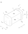
- FIG. 1 is a schematic perspective view of a multilayer ceramic capacitor.
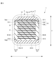
- 2 is a cross-sectional view taken along line II-II in FIG. 1.
- 3 is a cross-sectional view taken along line III-III in FIG. 1.
- FIG. 4 is an enlarged view of a region Q enclosed by a dotted square in FIG. 3 . This is the formula for calculating skewness.
- FIG. 1 is a schematic perspective view of a multilayer ceramic capacitor 100.
- 7 is a cross-sectional view taken along line VV in FIG. 6.
- 7 is a cross-sectional view taken along line VI-VI in FIG. 6.
- 7 is a cross-sectional view taken along line VII-VII in FIG. 6.
- 1 is a view of an inner layer portion 11 of a multilayer ceramic capacitor 100 as viewed from the first main surface A1 side, with the positions of an end surface exposed inner electrode 16 and a side surface exposed inner electrode 17 indicated by dotted lines.
- the multilayer ceramic capacitor 1 according to the first embodiment is a two-terminal multilayer ceramic capacitor.
- Fig. 1 is a schematic perspective view of the multilayer ceramic capacitor 1.
- Fig. 2 is a cross-sectional view taken along line II-II in Fig. 1.
- Fig. 3 is a cross-sectional view taken along line III-III in Fig. 1.
- the multilayer ceramic capacitor 1 has a substantially rectangular parallelepiped shape and includes a laminate 2 and a pair of end surface external electrodes 3 provided on both ends of the laminate 2.
- the laminate 2 includes an inner layer portion 11 in which a plurality of inner dielectric layers 14 and a plurality of end surface exposed internal electrodes 15 are laminated, and an outer layer portion 12.
- the direction in which the internal dielectric layers 14 and the end surface exposed internal electrodes 15 are stacked is referred to as the stacking direction T, as a term used to describe the orientation of the multilayer ceramic capacitor 1.
- the direction that intersects with the stacking direction T and in which the pair of end surface external electrodes 3 are arranged is referred to as the vertical direction L.
- the direction that intersects with both the vertical direction L and the stacking direction T is referred to as the horizontal direction W. Note that in the embodiment, the horizontal direction W is perpendicular to both the vertical direction L and the stacking direction T.
- a pair of outer peripheral surfaces facing each other in the stacking direction T will be referred to as the first main surface A1 and the second main surface A2, and when it is not necessary to distinguish between the first main surface A1 and the second main surface A2, they will be collectively referred to as the main surface A.
- a pair of outer peripheral surfaces facing each other in the horizontal direction W of the laminate 2 will be referred to as the first side surface B1 and the second side surface B2, and when it is not necessary to distinguish between the first side surface B1 and the second side surface B2, they will be collectively referred to as the side surface B.
- first end surface C1 and the second end surface C2 A pair of outer peripheral surfaces facing each other in the vertical direction L of the laminate 2 will be referred to as the first end surface C1 and the second end surface C2, and when it is not necessary to distinguish between the first end surface C1 and the second end surface C2, they will be collectively referred to as the end surface C.
- both or either of the first and second principal surfaces A1 and A2 be flat. If the principal surface A is flat, the stress received from the nozzle when picking up the multilayer ceramic capacitor 1 can be dispersed by the flat principal surface A, improving the strength of the multilayer ceramic capacitor 1 during mounting. However, this is not limited to this, and both the first and second principal surfaces A1 and A2 of the laminate 2 may be roughened.
- the portion where two of the first main surface A1, second main surface A2, first end surface C1, second end surface C2, first side surface B1, and second side surface B2 intersect is called a ridge portion, and the portion where three of the surfaces intersect is called a corner portion. It is preferable that the ridge portions and corner portions are rounded, as this helps prevent chipping and cracking. When the ridge portions and corner portions are rounded, the main surface may be flat on the surfaces excluding the corners and ridge portions.
- the inner layer portion 11 includes an end surface exposed internal electrode 15 and an inner dielectric layer 14 laminated alternately with the end surface exposed internal electrodes 15.
- the thickness of the end surface exposed internal electrodes 15 and the inner electrode 15 is preferably 0.25 ⁇ m or more and 0.6 ⁇ m or less.
- the end surface exposed internal electrode 15 includes a first end surface exposed internal electrode 15A having one end exposed on the first end surface C1 and a second end surface exposed internal electrode 15B having one end exposed on the second end surface C2.
- the first end surface exposed internal electrode 15A and the second end surface exposed internal electrode 15B are alternately stacked.
- the components of the end surface exposed internal electrode 15 can be, but are not limited to, suitable conductive materials such as metals such as Ni, Cu, Ag, Pd, and Au, and alloys containing at least one of these metals, such as Ag-Pd alloys. Furthermore, when the end surface exposed internal electrode 15 contains Sn, it is possible to reduce electric field concentration at the interface between the end surface exposed internal electrode 15 and the internal dielectric layer 14, leading to improved high temperature load reliability. In this case, even if Sn is contained in only one of the end surface exposed internal electrodes 15, either the first end surface exposed internal electrode 15A or the second end surface exposed internal electrode 15B, it can be sufficiently effective.
- the first end surface exposed internal electrode 15A has a first opposing portion 15Aa facing the second end surface exposed internal electrode 15B, and a first lead portion 15Ab drawn from the first opposing portion 15Aa onto the first end surface C1.
- the second end surface exposed internal electrode 15B has a second opposing portion 15Ba facing the first end surface exposed internal electrode 15A, and a second lead portion 15Bb drawn from the second opposing portion 15Ba onto the second end surface C2.
- the first opposing portion 15Aa and the second opposing portion 15Ba face each other, and a capacitance is formed between the first opposing portion 15Aa and the second opposing portion 15Ba. This allows the multilayer ceramic capacitor 1 to exhibit the characteristics of a capacitor.
- first opposing portion 15Aa and the second opposing portion 15Ba they will be collectively referred to as opposing portion 15a.
- first pull-out portion 15Ab and the second pull-out portion 15Bb they will be collectively referred to as pull-out portion 15b.
- the internal dielectric layer 14 contains barium titanate as a main component and Si as a sub-component.
- the thickness of the internal dielectric layer 14 in the stacking direction T is 0.45 ⁇ m or less.
- the internal dielectric layer 14 constituting the inner layer portion 11 of the multilayer ceramic capacitor 1 contains ceramic grains.
- the ceramic grain diameter D50 of the internal dielectric layer 14 is preferably 0.15 ⁇ m or less. This allows the number of ceramic grains contained in the internal dielectric layer 14 to be increased, increasing the number of interfaces between the ceramic grains and improving high-temperature reliability.
- the region between the end surface exposed internal electrode 15 and the side surface B in the inner layer portion 11 is defined as the gap region D1.
- the region between the first end surface exposed internal electrode 15A and the second end surface C2, and the region between the second end surface exposed internal electrode 15B and the first end surface C1, i.e., the region in the inner layer portion 11 where the pull-out portion 15b exists in the stacking direction T are defined as the pull-out region D2.
- the Si content of the internal dielectric layer 14 located in the gap region D1 and near the center of the stacking direction T is preferably 0.2 at% (atomic percent) or more and 5.0 at% or less.
- the Si content in the dielectric ceramic in the gap region D1 is less than 0.2 at%, sintering is difficult to proceed.
- the Si content in the dielectric ceramic in the gap region D1 is 0.2 at% or more, so the sinterability of the internal dielectric layer 14 can be improved. This reduces the possibility of moisture penetrating from the first side B1 and second side B2, which are not covered by the end face external electrode 3, and reaching the end face exposed internal electrode 15, thereby improving moisture resistance.
- the Si content in the dielectric ceramic in the gap region D1 is greater than 5.0 at%, the capacitance reduction due to the decrease in dielectric constant becomes significant, which is not preferable.
- the Si content in the dielectric ceramic in the gap region D1 is 5.0 at% or less, so the problem of capacitance reduction due to the decrease in dielectric constant is unlikely to occur.
- the Si content of the internal dielectric layer 14 located near the center of the stacking direction T in the gap region D1 is set to 0.2 at% or more and 5.0 at% or less, but this is not limited thereto. As long as the Si content of the internal dielectric layer 14 located near the center of the stacking direction T in at least the gap region D1 is 0.2 at% or more and 5.0 at% or less, the possibility of moisture penetrating from the first side surface B1 and the second side surface B2 that are not covered by the end face external electrode 3 and reaching the end face exposed internal electrode 15 can be reduced.
- the Si content can be measured as follows. For example, in the case of gap region D1, in the cross section near the center in the vertical direction L shown in Figure 3, a region of ⁇ 1 ⁇ m located 5 ⁇ m outward in the horizontal direction W (toward side B) from the end of end-face exposed internal electrode 15 at a position approximately halfway in the stacking direction T is defined as P.
- the Si content is calculated from the X-ray intensity spectrum detected by a WDX (wavelength dispersive X-ray fluorescence analyzer) within this region P.
- the laminate 2 has an inner layer portion 11 and two outer layer portions 12 arranged to sandwich the inner layer portion 11 in the stacking direction T.
- the outer layer portion 12 on the first main surface A1 side is referred to as a first outer layer portion 12a
- the outer layer portion 12 on the second main surface A2 side is referred to as a second outer layer portion 12b.
- the first outer layer portion 12a and the second outer layer portion 12b are each formed from an insulating material.
- the first outer layer portion 12a and the second outer layer portion 12b are arranged by being pressed so as to wrap around the gap region D1 and the lead-out region D2.
- FIG. 4 is an enlarged view of the area Q enclosed by a dotted line in FIG. 3.
- Both the outer layer 12 and the gap area D1 contain voids q.
- the porosity of the outer layer 12 is lower than that of the gap area D1.
- the porosity is the ratio of the area of voids q per unit cross-sectional area. The porosity is measured by binarizing the voids q and other areas in an observation image with an observation field of view of 10 ⁇ m square.
- the outer layer portions 12 are laminated on both sides of the gap region D1 in the lamination direction T. Therefore, even after firing in the manufacturing process of the multilayer ceramic capacitor, some kind of interface exists between the gap region D1 and the outer layer portions 12.
- the interface has a weaker bonding strength than other portions, and in particular, when the multilayer ceramic capacitor is miniaturized, in the case of a multilayer ceramic capacitor with a conventional structure, the dimension of the gap region D1 in the lateral direction W becomes smaller, so that moisture easily penetrates through this interface to the internal electrode 15.
- the outer layer 12 is pressed and positioned so that it wraps around the gap region D1, so that the interface between the gap region D1 and the outer layer 12 is compressed. This reduces the possibility that moisture from the outside will penetrate through the interface and reach the internal electrode 15, improving moisture resistance.
- the thickness of the internal dielectric layer 14 in the stacking direction T is 0.45 ⁇ m or less.
- the overall capacitance is improved.
- the outer layer 12 is pressed and positioned so that it wraps around the gap region D1. Therefore, even in the step portion, the interface between the outer layer 12 and the gap region D1 is strongly pressed. This further reduces the possibility that moisture from the outside will penetrate the interface and reach the internal electrode 15, improving moisture resistance.
- the outer layer 12 is arranged so that it wraps around the gap region D1, so that the interface between the outer layer 12 and the gap region D1 is curved rather than linear, and the distance of the interface is longer than if the outer layer 12 did not wrap around. This also reduces the possibility that moisture from the outside will penetrate the interface and reach the internal electrode 15, improving moisture resistance.
- the wraparound amount D11 of the first outer layer portion 12a into the gap region D1 is larger than the wraparound amount D12 of the second outer layer portion 12b into the gap region D1.
- the wraparound amount D12 of the second outer layer portion 12b be 90% or less of the wraparound amount D11 of the first outer layer portion 12a.
- the wraparound amount D12 of one of the outer layer parts 12 on the main surface side (the second outer layer part 12b in this embodiment), which is the side on which the board is mounted, is made too large, it is difficult to maintain flatness during mounting, which is not preferable.
- the outer layer 12 on the other main surface side that is not the board mounting side there is no problem with mounting even if the wraparound amount D11 is increased, and the moisture resistance is improved as the wraparound amount D11 is larger.
- the amount of current flowing into the pull-out region D2 of the outer layer 12, D21 and D22 is smaller than the amount of current flowing into the gap region D1, D11 and D12, so that the current path from the mounting land to the pull-out region D2 can be prevented from becoming too long. Therefore, the moisture resistance reliability can be improved without significantly increasing the ESL (equivalent series inductance).
- FIG. 6 is a schematic perspective view of the multilayer ceramic capacitor 100.
- FIG. 7 is a cross-sectional view taken along line V-V in FIG. 6.
- FIG. 8 is a cross-sectional view taken along line VI-VI in FIG. 6.
- FIG. 9 is a cross-sectional view taken along line VII-VII in FIG. 6.
- the multilayer ceramic capacitor 100 has a generally rectangular parallelepiped shape and is provided with a pair of end surface external electrodes 3 provided at both ends of the laminate 2, as well as a side surface external electrode 4.
- the inner layer portion 11 includes an end surface exposed inner electrode 16 and a side surface exposed inner electrode 17.
- Fig. 10 is a view of the inner layer portion 11 of the multilayer ceramic capacitor 100 viewed from the first main surface A1 side, and the positions of the end surface exposed inner electrodes 16 (16a, 16b) and the side surface exposed inner electrodes 17 (17a, 17b) are indicated by dotted lines.
- the end surface exposed internal electrode 16 extends between both end surfaces C in the longitudinal direction L of the laminate 2 and is spaced a fixed distance from both side surfaces B in the transverse direction W.
- the end surface exposed internal electrode 16 has an end surface facing portion 16a located in the center between both end surfaces C and an end surface drawn portion 16b extending from the end surface facing portion 16a to both end surfaces C.
- the end surface drawn portions 16b extend to both end surfaces C, respectively, are exposed at the end surfaces C of the laminate 2, and are connected to the end surface external electrodes 3 provided on both end surfaces in the longitudinal direction L of the laminate 2.
- the dimension of the end surface facing portion 16a in the horizontal direction W of the end surface exposed internal electrode 16 is smaller than the dimension of the end surface drawn portion 16b in the horizontal direction.
- the end surface drawn portion 16b may have a tapered shape so that the width (dimension in the vertical direction L) gradually decreases from the connection point with the end surface facing portion 16a.
- the side exposed internal electrode 17 extends between both side surfaces B in the horizontal direction W of the laminate 2 and is spaced apart from both end surfaces C in the vertical direction L.
- the side exposed internal electrode 17 has a side facing portion 17a located in the center between both side surfaces B, and a side drawn-out portion 17b extending from the side facing portion 17a to both side surfaces B.
- the dimension in the vertical direction L of the side drawn-out portion 17b is smaller than the dimension in the vertical direction L of the side facing portion 17a.
- the side drawn-out portion 17b extends to both side surfaces B, is exposed at the side surface B of the laminate 2, and is connected to the side external electrodes 4 provided on both side surfaces in the horizontal direction W of the laminate 2.
- End surface external electrode 3 End surface external electrodes 3 are disposed on both end surfaces C of the laminate 2. End surface drawn portions 16b of end surface exposed internal electrodes 16 are connected to the end surface external electrodes 3. The end surface external electrodes 3 cover not only the end surfaces C but also parts of the main surfaces A and side surfaces B on the end surface C side.
- Side surface external electrodes 4 are disposed on both side surfaces B of the laminate 2. Side surface drawn portions 17b of side surface exposed internal electrodes 17 are connected to the side surface external electrodes 4. The side surface external electrodes 4 cover not only the side surface B but also a portion of the main surface A on the side surface B side.
- the region of the inner layer 11 where the end surface drawn-out portion 16b is laminated is defined as the end surface drawn-out region E1.
- the region where the side surface drawn-out portion 17b is laminated is defined as the side surface drawn-out region E2.
- the region between the end surface exposed internal electrode 16 and the side surface B, other than the side surface drawn-out region E2, is defined as the three-terminal gap region E3.
- the outer layer 12 is arranged so as to wrap around the three-terminal gap region E3, the end face pull-out region E1, and the side face pull-out region E2.
- wraparound amount E31 of the first outer layer 12a into the three-terminal gap region E3 shown in FIG. 9 is greater than the wraparound amount E11 of the first outer layer 12a into the end face pull-out region E1 shown in FIG. 7 or the wraparound amount E21 into the side face pull-out region E2 shown in FIG. 8.
- the amount E32 of the second outer layer 12b wrapping around the three-terminal gap region E3 shown in FIG. 9 is greater than the amount E12 of the second outer layer 12b wrapping around the end face pull-out region E1 shown in FIG. 7, or the amount E22 of the second outer layer 12b wrapping around the side face pull-out region E2 shown in FIG. 8.
- the multilayer ceramic capacitor 100 of the second embodiment can achieve the following effects in the same way as the first embodiment.
- the outer layer 12 is pressed so as to wrap around the three-terminal gap region E3, the end face pull-out region E1, and the side face pull-out region E2, so that the interfaces between the three-terminal gap region E3, the end face pull-out region E1, and the side face pull-out region E2 and the outer layer 12 are compressed. This reduces the possibility that moisture from the outside will penetrate the interfaces and reach the internal electrodes 16 and 17, improving moisture resistance.
- the wraparound amount of the first outer layer 12a is greater than the wraparound amount of the second outer layer 12b, so that flatness is maintained during mounting while moisture resistance is improved to the maximum.
- the end surface exposed internal electrode is an opposing portion facing the adjacent end surface exposed internal electrode in the lamination direction; a lead portion led from the facing portion to one of the two end faces,
- the outer layer portion is The pull-out area is arranged so as to wrap around the pull-out area,
- the amount of the first outer layer portion wrapping around the gap region is The multilayer ceramic capacitor according to any one of ⁇ 1> to ⁇ 4>, wherein the amount of wrapping around the first outer layer portion into the lead region is larger than the amount of wrapping around the first outer layer portion into the lead region.
- a laminate having a first main surface and a second main surface opposed to each other in a stacking direction, two end surfaces opposed to each other in a vertical direction intersecting the stacking direction, and two side surfaces opposed to each other in a horizontal direction intersecting the stacking direction and the vertical direction;
- Two end surface external electrodes are disposed on the two end surfaces of the laminate, respectively;
- two side surface external electrodes respectively disposed on the two side surfaces of the laminate;
- the laminate comprises: The inner layer and and outer layer portions arranged to sandwich the inner layer portion in the stacking direction, The outer layer portion is A first outer layer portion located on the first main surface side; A second outer layer portion located on the second main surface side,
- the inner layer portion is A plurality of end surface exposed internal electrodes; A plurality of side exposed internal electrodes; a plurality of inner dielectric layers;
- the end surface exposed internal electrodes are an end face facing portion facing the side surface exposed internal electrode in the lamination direction; an end surface drawn-out portion drawn from the end surface facing portion to the end surface of
- the outer layer portion is The end surface extraction region and the side surface extraction region are arranged so as to wrap around the end surface extraction region and the side surface extraction region,
- the amount of wraparound of the outer layer portion into the three-terminal gap region is The multilayer ceramic capacitor according to ⁇ 6>, wherein the amount of wrapping around the outer layer portion is larger than the amount of wrapping around the end surface drawn-out region or the side surface drawn-out region.
- the ceramic grain diameter D50 of the internal dielectric layer is 0.15 ⁇ m or less.
- the thickness of the internal dielectric layer in the lamination direction is 0.45 ⁇ m or less.
- the porosity of the outer layer portion is lower than the porosity of the gap region or the three-terminal gap region, ⁇ 1>.
Landscapes
- Engineering & Computer Science (AREA)
- Power Engineering (AREA)
- Manufacturing & Machinery (AREA)
- Microelectronics & Electronic Packaging (AREA)
- Fixed Capacitors And Capacitor Manufacturing Machines (AREA)
- Ceramic Capacitors (AREA)
Abstract
小型化及び薄層化が可能で、且つ、耐湿性の向上が可能な積層セラミックコンデンサを提供する。本発明の積層セラミックコンデンサ1は、積層体2の2つの端面Cにそれぞれ配置された2つの端面外部電極3と、を具備し、積層体2は、内層部11と、内層部11を積層方向に挟み込むように配置された外層部12と、を備え、内層部11は、複数の端面露出内部電極15と、複数の内部誘電体層14と、を含み、外層部12は、第1主面A1側に位置する第1外層部12aと、第2主面A2側に位置する第2外層部12bと、を含み、外層部12は、端面露出内部電極15と側面との間のギャップ領域D1まで回り込むように配置され、第1外層部12aのギャップ領域D1への回り込み量は、第2外層部12bのギャップ領域D1への回り込み量よりも大きい。
Description
本発明は、積層セラミックコンデンサに関する。
積層セラミックコンデンサは、一般的に内部電極と誘電体層とが交互に積層された内層部を有する。内層部における積層方向の両側には外層部が配置され、内層部における容量形成に寄与する有効層の、積層方向と直交する方向の外周部には、容量形成に寄与しないギャップ部が設けられている。これらの外層部やギャップ部は、耐湿性などの信頼性に寄与している。
また、近年、積層セラミックコンデンサも小型化及び薄層化が求められている一方、大容量化も求められている。内層部は容量に寄与するために小型化には限界がある。なので、全体的に小型化及び薄層化を図るためには、外層部やギャップ部のさらなる薄層化が図られる。
しかし、外層部やギャップ部が薄層化されると信頼性が低下する可能性がある。このため、外層部の外側をカバーするように絶縁層を配置している従来技術がある(特許文献1参照)。
しかし、上記従来技術のように、外層部の外側をカバーするように絶縁層を配置する場合、さらなる絶縁層配置工程が必要となり、また、絶縁層の分だけ積層体が厚くなる。
本発明は、小型化及び薄層化が可能で、且つ、耐湿性の向上が可能な、積層セラミックコンデンサを提供することを目的とする。
上記課題を解決するために本発明は、積層方向に相対する第1主面及び第2主面と、前記積層方向と交差する縦方向に相対する2つの端面と、前記積層方向及び前記縦方向と交差する横方向に相対する2つの側面とを有する積層体と、前記積層体の2つの前記端面にそれぞれ配置された2つの端面外部電極と、を具備し、前記積層体は、内層部と、前記内層部を前記積層方向に挟み込むように配置された外層部と、を備え、前記内層部は、複数の端面露出内部電極と、複数の内部誘電体層と、を含み、前記外層部は、前記第1主面側に位置する第1外層部と、前記第2主面側に位置する第2外層部と、を含み、前記外層部は、前記端面露出内部電極と前記側面との間のギャップ領域まで回り込むように配置され、前記第1外層部の前記ギャップ領域への回り込み量は、前記第2外層部の前記ギャップ領域への回り込み量よりも大きい、積層セラミックコンデンサを提供する。
さらに、上記課題を解決するために本発明は、積層方向に相対する第1主面及び第2主面と、前記積層方向と交差する縦方向に相対する2つの端面と、前記積層方向及び前記縦方向と交差する横方向に相対する2つの側面とを有する積層体と、前記積層体の2つの前記端面にそれぞれ配置された2つの端面外部電極と、前記積層体の2つの前記側面にそれぞれ配置された2つの側面外部電極と、を具備し、前記積層体は、内層部と、前記内層部を前記積層方向に挟み込むように配置された外層部と、備え、前記外層部は、前記第1主面側に位置する第1外層部と、前記第2主面側に位置する第2外層部と、を含み、前記内層部は、複数の端面露出内部電極と、複数の側面露出内部電極と、複数の内部誘電体層と、を含み、前記端面露出内部電極は、前記側面露出内部電極と前記積層方向に対向する端面対向部と、前記端面対向部から前記積層体の前記端面に引き出される端面引出部と、を有し、前記側面露出内部電極は、前記端面露出内部電極と前記積層方向に対向する側面対向部と、前記側面対向部から積層体の前記側面に引き出される側面引出部と、を有し、前記内層部において、前記積層方向に、前記端面引出部が重なる領域を端面引出領域、前記側面引出部が重なる領域を側面引出領域、前記端面露出内部電極と前記側面との間の領域であり、且つ前記側面引出領域と重ならない領域を三端子ギャップ領域としたときに、前記外層部は、前記三端子ギャップ領域まで回り込むように配置され、前記三端子ギャップ領域における、前記第1外層部の回り込み量は、前記第2外層部の回り込み量よりも大きい、積層セラミックコンデンサを提供する。
本発明によれば、小型化及び薄層化が可能で、且つ、耐湿性の向上が可能な、積層セラミックコンデンサを提供することができる。
(第1実施形態)
以下、本発明の第1実施形態にかかる積層セラミックコンデンサ1について説明する。第1実施形態にかかる積層セラミックコンデンサ1は、二端子型積層セラミックコンデンサである。図1は、積層セラミックコンデンサ1の概略斜視図である。図2は、図1のII-II線に沿った断面図である。図3は、図1のIII-III線に沿った断面図である。
以下、本発明の第1実施形態にかかる積層セラミックコンデンサ1について説明する。第1実施形態にかかる積層セラミックコンデンサ1は、二端子型積層セラミックコンデンサである。図1は、積層セラミックコンデンサ1の概略斜視図である。図2は、図1のII-II線に沿った断面図である。図3は、図1のIII-III線に沿った断面図である。
(積層セラミックコンデンサ1)
積層セラミックコンデンサ1は、略直方体形状で、積層体2と、積層体2の両端に設けられた一対の端面外部電極3とを備える。積層体2は、複数の内部誘電体層14と複数の端面露出内部電極15とが積層された内層部11と、外層部12とを含む。
積層セラミックコンデンサ1は、略直方体形状で、積層体2と、積層体2の両端に設けられた一対の端面外部電極3とを備える。積層体2は、複数の内部誘電体層14と複数の端面露出内部電極15とが積層された内層部11と、外層部12とを含む。
以下の説明において、積層セラミックコンデンサ1の向きを表わす用語として、内部誘電体層14と端面露出内部電極15とが積層されている方向を積層方向Tとする。積層方向Tと交差するとともに一対の端面外部電極3が配置されている方向を縦方向Lとする。縦方向L及び積層方向Tのいずれにも交差する方向を横方向Wとする。なお、実施形態においては、横方向Wは縦方向L及び積層方向Tのいずれにも直交している。
(積層体2)
また、以下の説明において、図2に示す積層体2の6つの外周面のうち、積層方向Tに相対する一対の外周面を第1主面A1と第2主面A2とし、第1主面A1と第2主面A2とを特に区別して説明する必要のない場合、まとめて主面Aとして説明する。積層体2の横方向Wに相対する一対の外周面を第1側面B1と第2側面B2とし、第1側面B1と第2側面B2とを特に区別して説明する必要のない場合、まとめて側面Bとして説明する。積層体2の縦方向Lに相対する一対の外周面を第1端面C1と第2端面C2とし、第1端面C1と第2端面C2とを特に区別して説明する必要のない場合、まとめて端面Cとして説明する。
また、以下の説明において、図2に示す積層体2の6つの外周面のうち、積層方向Tに相対する一対の外周面を第1主面A1と第2主面A2とし、第1主面A1と第2主面A2とを特に区別して説明する必要のない場合、まとめて主面Aとして説明する。積層体2の横方向Wに相対する一対の外周面を第1側面B1と第2側面B2とし、第1側面B1と第2側面B2とを特に区別して説明する必要のない場合、まとめて側面Bとして説明する。積層体2の縦方向Lに相対する一対の外周面を第1端面C1と第2端面C2とし、第1端面C1と第2端面C2とを特に区別して説明する必要のない場合、まとめて端面Cとして説明する。
第1主面A1及び第2主面A2の両主面A、もしくは、一方の主面Aは平坦であることが好ましい。平坦であると積層セラミックコンデンサ1をピックアップする際、ノズルから受ける応力を平らな主面Aで分散させることができるため、実装時において積層セラミックコンデンサ1の強度を向上させることができる。ただし、これに限定されず、積層体2の第1主面A1及び第2主面A2の両主面Aは粗されていてもよい。
第1主面A1、第2主面A2、第1端面C1、第2端面C2、第1側面B1、第2側面B2のうち二面が交わる部分を稜線部、三面が交わる部分を角部と呼ぶ。稜線部及び角部にはRが付けられていることが好ましく、Rが付いていることによってかけ割れを防止することができる。稜線部及び角部にRがつけられている時、角部と稜線部とを除く面において主面が平坦であってもよい。
(内層部11)
内層部11は、端面露出内部電極15と、端面露出内部電極15と交互に積層された内部誘電体層14とを含む。端面露出内部電極15及び端面露出内部電極15の内部電極15の厚みは、0.25μm以上0.6μm以下が好ましい。
内層部11は、端面露出内部電極15と、端面露出内部電極15と交互に積層された内部誘電体層14とを含む。端面露出内部電極15及び端面露出内部電極15の内部電極15の厚みは、0.25μm以上0.6μm以下が好ましい。
(端面露出内部電極15)
端面露出内部電極15は、第1端面C1上に一端が露出された第1端面露出内部電極15Aと、第2端面C2上に一端が露出された第2端面露出内部電極15Bと、を備える。第1端面露出内部電極15Aと第2端面露出内部電極15Bとは、交互に積層されている。
端面露出内部電極15は、第1端面C1上に一端が露出された第1端面露出内部電極15Aと、第2端面C2上に一端が露出された第2端面露出内部電極15Bと、を備える。第1端面露出内部電極15Aと第2端面露出内部電極15Bとは、交互に積層されている。
端面露出内部電極15の成分として、例えば、Ni、Cu、Ag、Pd、Auなどの金属や、Ag-Pd合金等の、それらの金属の少なくとも一種を含む合金などの適宜の導電材料により構成することができるが、これに限定されない。また、端面露出内部電極15がSnを含むと、端面露出内部電極15と内部誘電体層14との界面への電界集中を緩和でき、高温負荷信頼性向上に繋がる。このとき、Snは、第1端面露出内部電極15A及び第2端面露出内部電極15Bのいずれか片方の端面露出内部電極15のみに含まれていても十分に効果を発揮することができる。
第1端面露出内部電極15Aは、第2端面露出内部電極15Bと対向している第1対向部15Aaと、第1対向部15Aaから第1端面C1上に引き出される第1引出部15Abとを有している。第2端面露出内部電極15Bは、第1端面露出内部電極15Aと対向している第2対向部15Baと、第2対向部15Baから第2端面C2上に引き出される第2引出部15Bbとを有している。
第1対向部15Aaと第2対向部15Baとは互いに対向し、第1対向部15Aaと第2対向部15Baとの間に容量が形成される。これにより、積層セラミックコンデンサ1にコンデンサの特性が発現する。
なお、第1対向部15Aaと第2対向部15Baとを特に区別して説明する必要のない場合、まとめて対向部15aとして説明する。また、第1引出部15Abと第2引出部15Bbとを特に区別して説明する必要のない場合、まとめて引出部15bとして説明する。
(内部誘電体層14)
内部誘電体層14は、主成分としてのチタン酸バリウムと、副成分としてのSiとを含む。また、内部誘電体層14の積層方向Tの厚みは、0.45μm以下である。
内部誘電体層14は、主成分としてのチタン酸バリウムと、副成分としてのSiとを含む。また、内部誘電体層14の積層方向Tの厚みは、0.45μm以下である。
(セラミックグレイン)
積層セラミックコンデンサ1の内層部11を構成する内部誘電体層14はセラミックグレインを含む。内部誘電体層14のセラミックグレイン径D50は、0.15μm以下であることが好ましい。これにより、内部誘電体層14に含まれるセラミックグレインの個数を多くすることができるため、セラミックグレイン同士の界面が増え、高温信頼性が向上する。
積層セラミックコンデンサ1の内層部11を構成する内部誘電体層14はセラミックグレインを含む。内部誘電体層14のセラミックグレイン径D50は、0.15μm以下であることが好ましい。これにより、内部誘電体層14に含まれるセラミックグレインの個数を多くすることができるため、セラミックグレイン同士の界面が増え、高温信頼性が向上する。
ここで、図3に示すように内層部11における、端面露出内部電極15と側面Bとの間の領域をギャップ領域D1とする。また、図2に示すように、第1端面露出内部電極15Aと第2端面C2との間の領域、及び、第2端面露出内部電極15Bと第1端面C1との間の領域、すなわち、内層部11における積層方向Tに引出部15bが存在する領域を引出領域D2とする。
本実施形態において、ギャップ領域D1内、且つ、積層方向Tの中央付近に位置している内部誘電体層14のSiの含有量は、0.2at%(アトミックパーセント)以上5.0at%以下であることが好ましい。
ギャップ領域D1における誘電体セラミック中のSiの含有率が0.2at%より少ない場合、焼結が進みにくい。しかし、本願においては、ギャップ領域D1における誘電体セラミック中のSiの含有率が、0.2at%以上であるので、内部誘電体層14の焼結性を高めることができる。これによって、特に端面外部電極3により覆われていない第1側面B1及び第2側面B2から水分が侵入して端面露出内部電極15に到達する可能性を低下させることができるため、耐湿性が向上する。
また、ギャップ領域D1における誘電体セラミック中のSiの含有率が5.0at%より多い場合、誘電率低下に伴う静電容量低下が顕著となるので好ましくない。しかし、本願においては、ギャップ領域D1における誘電体セラミック中のSiの含有率が5.0at%以下であるので、誘電率低下による静電容量低下の問題が生じにくい。
なお、実施形態においては、ギャップ領域D1において積層方向Tの中央付近に位置している内部誘電体層14のSiの含有量は、0.2at%以上5.0at%以下としたが、これに限定されず、少なくともギャップ領域D1において積層方向Tの中央付近に位置している内部誘電体層14のSiの含有量は、0.2at%以上5.0at%以下であれば、端面外部電極3により覆われていない第1側面B1及び第2側面B2から水分が侵入して端面露出内部電極15に到達する可能性を低下させることができる。
Siの含有量は、下記のように測定することができる。例えばギャップ領域D1の場合、図3で示す縦方向Lの中央付近の断面において、積層方向Tの約1/2の位置での、端面露出内部電極15の端部から横方向Wの外側(側面B側)に向かって5μmの位置におけるφ1μmの領域をPとする。この領域P内においてWDX(波長分散型蛍光X線分析装置)によって検出されたX線強度スペクトルからSiの含有量を算出する。
(外層部12)
積層体2は、内層部11と、内層部11を積層方向Tに挟み込むように配置された2つの外層部12を有している。2つの外層部12のうち第1主面A1側の外層部12を第1外層部12a、第2主面A2側の外層部12を第2外層部12bとする。第1外層部12a、第2外層部12bとは、それぞれ絶縁性の材料によって形成される。
積層体2は、内層部11と、内層部11を積層方向Tに挟み込むように配置された2つの外層部12を有している。2つの外層部12のうち第1主面A1側の外層部12を第1外層部12a、第2主面A2側の外層部12を第2外層部12bとする。第1外層部12a、第2外層部12bとは、それぞれ絶縁性の材料によって形成される。
(外層部12の回り込み)
実施形態の積層セラミックコンデンサ1において、第1外層部12a及び第2外層部12bは、ギャップ領域D1、及び、引出領域D2に回り込むように押圧されて配置されている。
実施形態の積層セラミックコンデンサ1において、第1外層部12a及び第2外層部12bは、ギャップ領域D1、及び、引出領域D2に回り込むように押圧されて配置されている。
図4は、図3における点線で四角く囲んだ領域Qの拡大図である。外層部12及びギャップ領域D1は、共に空隙qを含む。外層部12における空隙率は、ギャップ領域D1の空隙率よりも低い。空隙率は、単位断面積あたりの空隙qの面積の割合である。空隙率の測定方法は、観察視野10μm角においての観察像において、空隙qとその他とを二値化することによって算出する。
(回り込みの効果)
外層部12はギャップ領域D1の積層方向Tの両側に積層されたものである。ゆえに、積層セラミックコンデンサの製造工程において焼成された後においても、ギャップ領域D1と外層部12との間にはなんらかの界面が存在する。界面は、他の部分よりも結合強度が弱く、特に、積層セラミックコンデンサが小型化されると、従来構造の積層セラミックコンデンサの場合、ギャップ領域D1の横方向Wの寸法が小さくなるので、この界面を介して水分が内部電極15まで侵入しやすくなる。
外層部12はギャップ領域D1の積層方向Tの両側に積層されたものである。ゆえに、積層セラミックコンデンサの製造工程において焼成された後においても、ギャップ領域D1と外層部12との間にはなんらかの界面が存在する。界面は、他の部分よりも結合強度が弱く、特に、積層セラミックコンデンサが小型化されると、従来構造の積層セラミックコンデンサの場合、ギャップ領域D1の横方向Wの寸法が小さくなるので、この界面を介して水分が内部電極15まで侵入しやすくなる。
しかし、実施形態の積層セラミックコンデンサ1においては、外層部12が、ギャップ領域D1まで回り込むように押圧されて配置されているので、ギャップ領域D1と外層部12との間の界面が圧着される。したがって、外部からの水分が、界面を伝わって、内部電極15まで進入する可能性が低くなり、耐湿性が向上する。
また、図3に示すように、ギャップ領域D1は、内部電極15が配置されていない。ゆえに内部電極15と内部誘電体層14とが積層されている中央の対応領域と比べて、内部電極15の分だけ積層方向Tの厚みが薄くなる。そうすると、ギャップ領域D1と、対応領域との間で段差が形成される。
実施形態において内部誘電体層14の積層方向Tの厚みは、0.45μm以下である。このように内部誘電体層14の1層当たりの厚みが薄いと、全体としての静電容量が向上する。
しかし、内部誘電体層14が内部電極15に対して相対的に薄くなると、対向部の積層方向T全体の厚みにおける内部電極15の占める割合が大きくなる。そうすると、内部電極15の有無により生じる段差の、積層体2全体としての積層方向Tの厚みに対する影響が大きくなるこのため、後述の積層シートの積層方向Tへのプレス時において、段差部での、内部誘電体層14と外層部12との間の密着が不十分となりやすい。
しかし、実施形態の積層セラミックコンデンサ1においては、外層部12が、ギャップ領域D1まで回り込むように押圧されて配置されている。ゆえに、段差部においても外層部12とギャップ領域D1との間の界面が強く圧着される。したがって、外部からの水分が、界面を伝わって、内部電極15まで進入する可能性がさらに低くなり、耐湿性が向上する。
また、外層部12が、ギャップ領域D1まで回り込むように配置され、外層部12とギャップ領域D1との界面が直線的ではなく湾曲し、且つ回り込まない場合と比べて界面に距離が長くなる。これによっても、外部からの水分が、界面を伝わって、内部電極15まで進入する可能性が低くなり、耐湿性が向上する。
(第1外層部12aと第2外層部12bとの回り込み量の差)
また、実施形態において、第1外層部12aのギャップ領域D1への回り込み量D11、第2外層部12bのギャップ領域D1への回り込み量D12よりも大きい。例えば、第1外層部12aの回り込み量D11に対して、第2外層部12bの回り込み量D12を90%以下となるようにすることが好ましい。
また、実施形態において、第1外層部12aのギャップ領域D1への回り込み量D11、第2外層部12bのギャップ領域D1への回り込み量D12よりも大きい。例えば、第1外層部12aの回り込み量D11に対して、第2外層部12bの回り込み量D12を90%以下となるようにすることが好ましい。
なお、外層部12のギャップ領域D1への回り込み量D11は、大きいほうが耐湿性は向上することができる。しかし、基板実装側である一方の主面側外層部12(実施形態では第2外層部12b)の回り込み量D12をあまり大きくすると、実装時に平坦性が保ちにくいので好ましくない。
しかし、基板実装側ではない他方の主面側外層部12(実施形態では第1外層部12a)は、回り込み量D11を大きくしても実装に問題はなく、回り込み量D11が大きいほうが耐湿性は向上する。
ゆえに、本実施形態の積層セラミックコンデンサ1においては、第1外層部12aの回り込み量D11を第2外層部12bの回り込み量D12よりもよりも大きくする。これにより、実装時に平坦性を保ちつつ、耐湿性を最大限向上させることができる。
(ギャップ領域D1と引出領域D2との回り込み量の差)
そして、図3に示す第1外層部12aのギャップ領域D1への回り込み量D11は、図2に示す引出領域である引出領域D2への回り込み量D21よりも大きい。また、図3に示す第2外層部12bのギャップ領域D1への回り込み量D12は、図2に示す引出領域D2への回り込み量D22よりも大きい。
そして、図3に示す第1外層部12aのギャップ領域D1への回り込み量D11は、図2に示す引出領域である引出領域D2への回り込み量D21よりも大きい。また、図3に示す第2外層部12bのギャップ領域D1への回り込み量D12は、図2に示す引出領域D2への回り込み量D22よりも大きい。
実施形態によると、外層部12の引出領域D2への回り込み量D21,D22が、ギャップ領域D1への回り込み量D11,D12より小さいので、実装ランドから引出領域D2への電流経路が長くなりすぎることを防止することができる。ゆえに、ESL(等価直列インダクタンス)をそれほど大きくすることなく、耐湿信頼性を向上させることができる。
(回り込み量の定義)
なお、各外層部12のギャップ領域D1への回り込み量D11,D12は、下記のように定義される。まず、図3に示す断面において、最も第1主面A1側の内部電極15の最表面から横方向Wに平行な直線TW1と、最も第2主面A2側の内部電極15の最表面から横方向Wに平行な直線TW2と、である互いに平行な2本の直線を引く。
そして、それらの直線TW1及び直線TW2と直交する、内部電極15の横方向Wの端部を通る直線と、積層体2の横方向Wの端部を通る直線と、である互いに平行な2本の直線を引く。これらの4本の直線で囲まれた領域内において、ギャップ領域D1の内部に入り込んでいる第1外層部12aの面積が、第1外層部12aのギャップ領域D1への回り込み量D11である。
同様に、ギャップ領域D1の内部に位置する第2外層部12bの面積が、第2外層部12bのギャップ領域D1への回り込み量D12である。
なお、各外層部12のギャップ領域D1への回り込み量D11,D12は、下記のように定義される。まず、図3に示す断面において、最も第1主面A1側の内部電極15の最表面から横方向Wに平行な直線TW1と、最も第2主面A2側の内部電極15の最表面から横方向Wに平行な直線TW2と、である互いに平行な2本の直線を引く。
そして、それらの直線TW1及び直線TW2と直交する、内部電極15の横方向Wの端部を通る直線と、積層体2の横方向Wの端部を通る直線と、である互いに平行な2本の直線を引く。これらの4本の直線で囲まれた領域内において、ギャップ領域D1の内部に入り込んでいる第1外層部12aの面積が、第1外層部12aのギャップ領域D1への回り込み量D11である。
同様に、ギャップ領域D1の内部に位置する第2外層部12bの面積が、第2外層部12bのギャップ領域D1への回り込み量D12である。
また、各外層部12の引出領域D2への回り込み量D21,D22は、下記のように定義される。まず、図2に示す断面において、最も第1主面A1側の内部電極15の最表面から縦方向Lに平行な直線TL1と、最も第2主面A2側の内部電極15の最表面から縦方向Lに平行な直線TL2と、である互いに平行な2本の直線を引く。
そして、それらの直線TL1及び直線TW2と直交する、内部電極15の縦方向Lの端部を通る直線と、積層体2の縦方向Lの端部を通る直線と、である互いに平行な2本の直線を引く。これらの4本の直線で囲まれた領域内において、引出領域D2の内部に入り込んでいる第1外層部12aの面積が、第1外層部12aの引出領域D2への回り込み量D21である。
同様に、引出領域D2の内部に入り込んでいる第2外層部12bの面積が、第2外層部12bの引出領域D2への回り込み量D22である。
そして、それらの直線TL1及び直線TW2と直交する、内部電極15の縦方向Lの端部を通る直線と、積層体2の縦方向Lの端部を通る直線と、である互いに平行な2本の直線を引く。これらの4本の直線で囲まれた領域内において、引出領域D2の内部に入り込んでいる第1外層部12aの面積が、第1外層部12aの引出領域D2への回り込み量D21である。
同様に、引出領域D2の内部に入り込んでいる第2外層部12bの面積が、第2外層部12bの引出領域D2への回り込み量D22である。
(回り込み量の検出)
なお、外層部12と内部誘電体層14との境界は、例えば、FE-WDX(電界放出型電子マイクロアナライザ)などで観察することにより、検出することができる。例えば、ギャップ領域D1に位置する内部誘電体層14に含まれるSiの量と、外層部12に含まれるSiとの量とが異なると、FE-WDXなどでSiの偏析によって境界を検出することができる。また、外層部12と内部誘電体層14との間の空隙率の差によっても、外層部12と内部誘電体層14との境界を検出することができる。
なお、外層部12と内部誘電体層14との境界は、例えば、FE-WDX(電界放出型電子マイクロアナライザ)などで観察することにより、検出することができる。例えば、ギャップ領域D1に位置する内部誘電体層14に含まれるSiの量と、外層部12に含まれるSiとの量とが異なると、FE-WDXなどでSiの偏析によって境界を検出することができる。また、外層部12と内部誘電体層14との間の空隙率の差によっても、外層部12と内部誘電体層14との境界を検出することができる。
実施形態において外層部12は、主成分としてのチタン酸バリウムと、副成分としてのSi及びMnを含む。
(歪度)
実施形態において、外層部12及びギャップ領域D1内の内部誘電体層14に含まれるSiの歪度は、0以上0.5以下であることが好ましい。これによって、高温信頼性に悪影響を与えることなく、耐湿性を向上させることができる。外層部12、第1側面B1及び第2側面B2からの水分が侵入して端面露出内部電極15に到達する可能性を低下させることができるため、耐湿性が向上する。
実施形態において、外層部12及びギャップ領域D1内の内部誘電体層14に含まれるSiの歪度は、0以上0.5以下であることが好ましい。これによって、高温信頼性に悪影響を与えることなく、耐湿性を向上させることができる。外層部12、第1側面B1及び第2側面B2からの水分が侵入して端面露出内部電極15に到達する可能性を低下させることができるため、耐湿性が向上する。
(歪度の定義)
なお、Siの歪度は、下記の方法によって算出した。
まず、積層セラミックコンデンサ1を図3に示す位置まで断面研磨し、WDXで各マスでのSiの検出強度を測定した。より具体的には、観察視野5μm角を、38×38マスに分割したときの、それぞれのマスでのX線強度スペクトルからSiの含有量を測定した。その後、Siの歪度を算出するために、図5で示す計算式を用いた。図5で示す計算式は、自動計算させることも可能である。図5で示す計算式は、分布が正規分布からどれだけ歪んでいるかを表す計算式で、左右対称性を示す指標である。なお、計算式中、サンプリングサイズn、各データxi(i:1,2,3・・・,n)の平均値をx、標準偏差をsとする。
なお、Siの歪度は、下記の方法によって算出した。
まず、積層セラミックコンデンサ1を図3に示す位置まで断面研磨し、WDXで各マスでのSiの検出強度を測定した。より具体的には、観察視野5μm角を、38×38マスに分割したときの、それぞれのマスでのX線強度スペクトルからSiの含有量を測定した。その後、Siの歪度を算出するために、図5で示す計算式を用いた。図5で示す計算式は、自動計算させることも可能である。図5で示す計算式は、分布が正規分布からどれだけ歪んでいるかを表す計算式で、左右対称性を示す指標である。なお、計算式中、サンプリングサイズn、各データxi(i:1,2,3・・・,n)の平均値をx、標準偏差をsとする。
(外層部12の歪度)
さらに、ギャップ領域D1内の内部誘電体層14に含まれるSiの歪度は、外層部12に含まれるSiの歪度よりも大きい。すなわち、ギャップ領域D1内の内部誘電体層14に含まれるSiの粒径は、外層部12に含まれるSiの粒径よりもばらつきが大きい。換言すると、外層部12に含まれるSiの粒径は、ギャップ領域D1内の内部誘電体層14に含まれるSiの粒径よりも均一である。さらに換言すると、ギャップ領域D1内の内部誘電体層14に含まれるSiは、外層部12に含まれるSiよりも顕著な偏析が存在する。
さらに、ギャップ領域D1内の内部誘電体層14に含まれるSiの歪度は、外層部12に含まれるSiの歪度よりも大きい。すなわち、ギャップ領域D1内の内部誘電体層14に含まれるSiの粒径は、外層部12に含まれるSiの粒径よりもばらつきが大きい。換言すると、外層部12に含まれるSiの粒径は、ギャップ領域D1内の内部誘電体層14に含まれるSiの粒径よりも均一である。さらに換言すると、ギャップ領域D1内の内部誘電体層14に含まれるSiは、外層部12に含まれるSiよりも顕著な偏析が存在する。
そして、ギャップ領域D1内の内部誘電体層14に含まれるSiの歪度は、外層部12に含まれるSiの歪度よりも0.5%以上大きくすることが好ましい。
Siの歪度が大きいほうが、耐湿性が向上するので、内部誘電体層14の耐湿性を向上させることができる。
Siの歪度が大きいほうが、耐湿性が向上するので、内部誘電体層14の耐湿性を向上させることができる。
(Mn含有量)
さらに、実施形態において、外層部12に含まれるMnの含有量は、ギャップ領域D1内、且つ、積層方向Tの中央付近に位置している内部誘電体層14のMnの含有量よりも多い。これにより、外層部12の高温信頼性をより向上させることができる。
外層部12に含まれるMnの含有量を多くすることにより、外層部の緻密性を向上して、耐湿信頼性を向上させることができる。
なお、Mnで外層のみ耐湿信頼性を高めることによりギャップ領域D1の空隙率が相対的に高くなり、耐湿性が低くなるため、ギャップ領域D1はSiの偏析により耐湿信頼性を高めている。
さらに、実施形態において、外層部12に含まれるMnの含有量は、ギャップ領域D1内、且つ、積層方向Tの中央付近に位置している内部誘電体層14のMnの含有量よりも多い。これにより、外層部12の高温信頼性をより向上させることができる。
外層部12に含まれるMnの含有量を多くすることにより、外層部の緻密性を向上して、耐湿信頼性を向上させることができる。
なお、Mnで外層のみ耐湿信頼性を高めることによりギャップ領域D1の空隙率が相対的に高くなり、耐湿性が低くなるため、ギャップ領域D1はSiの偏析により耐湿信頼性を高めている。
(端面外部電極3)
端面外部電極3は、第1端面外部電極3Aと第2端面外部電極3Bとを備える。第1端面外部電極3Aは、第1端面露出内部電極15Aに接続され、第1端面C1上に配置されている。第1端面外部電極3Aは、主面及び側面Bの一部に延びる折返部も備える。第2端面外部電極3Bは、第2端面露出内部電極15Bに接続され、第2端面C2上に配置されている。第2端面外部電極3Bは、主面及び側面Bの一部に延びる折返部も備える。以下、第1端面外部電極3Aと第2端面外部電極3Bとを特に区別して説明する必要のない場合、まとめて端面外部電極3として説明する。
端面外部電極3は、第1端面外部電極3Aと第2端面外部電極3Bとを備える。第1端面外部電極3Aは、第1端面露出内部電極15Aに接続され、第1端面C1上に配置されている。第1端面外部電極3Aは、主面及び側面Bの一部に延びる折返部も備える。第2端面外部電極3Bは、第2端面露出内部電極15Bに接続され、第2端面C2上に配置されている。第2端面外部電極3Bは、主面及び側面Bの一部に延びる折返部も備える。以下、第1端面外部電極3Aと第2端面外部電極3Bとを特に区別して説明する必要のない場合、まとめて端面外部電極3として説明する。
端面外部電極3は、下地電極層31と、下地電極層31上に配置されためっき層32とを含む。下地電極層31は、例えば金属及びガラス成分を含む。金属は、例えば、銅、ニッケル、銀、パラジウム、銀-パラジウム合金、金などから選ばれる少なくとも1つを含み、実施形態では銅である。ガラス成分は、例えば、ホウ素及びケイ素を含む。めっき層32は、下地電極層31の上に配置されたNi(ニッケル)めっき層と、Niめっき層の上に配置されたSn(錫)めっき層とを含んでもよい。
(積層セラミックコンデンサ1の製造方法)
(Siの歪度の調整方法)
外層部12中とギャップ領域D1中のSiの歪度は、外層部用誘電体ペースト及び内部誘電体層用の誘電体ペーストに含ませるSiを含む粒子、例えばガラス粒子の粒径に差を設けることによって異ならせることができる。
(Siの歪度の調整方法)
外層部12中とギャップ領域D1中のSiの歪度は、外層部用誘電体ペースト及び内部誘電体層用の誘電体ペーストに含ませるSiを含む粒子、例えばガラス粒子の粒径に差を設けることによって異ならせることができる。
具体的には、外部誘電体層用の誘電体ペーストに基準とするガラス粒子を0.005μm以上0.5μm以下とした時に、それよりも粒径が1.0μm程度大きいガラス粒子を0.01Vol%以上40Vol%以下内部誘電体層用の誘電体ペーストに混合させる。一方、外層部用誘電体ペースト中のガラス粒子は、粒径を0.005μm以上0.5μm以下として含有させる。
そして、内部誘電体層用の誘電体ペーストを用いて作製された誘電体シート上に、内部電極用の導電性ペーストを、例えば所定のパターンで印刷することにより、誘電体シート上に内部電極パターンを形成する。内部電極パターンの形成方法としては、スクリーン印刷又はグラビア印刷等を用いることができる。
次に、外層部用誘電体ペーストを用いて作製された、第2外層部用誘電体シートを所定枚数積層する。その上に、内部電極パターンが印刷された内層部用の誘電体シートを順次積層する。さらにその上に、外層部用誘電体ペーストを用いて作製された、第1外層部用誘電体シートを所定枚数積層する。これにより、積層シートが作製される。
次に、静水圧プレス等の手段により、積層シートを積層方向Tにプレスし、積層ブロックを作製する。
この静水圧プレスの際、例えば、互いに隣接する積層体2の間に配置される部分が、他の部分より厚いラバーを、積層シートを積層方向Tに挟み込むように配置し、プレスを行うことで、外層部12をギャップ領域D1や引出領域D2に回り込ませることができる。
そして、静水圧プレスの際、第1主面A1側と第2主面A2側とで硬度、厚みが異なるラバーを用いてプレスを行うことで、第1外層部12aの回り込み量が第2外層部12bの回り込み量より多くなるようにすることができる。例えば、第2主面A2側のラバーを固くすると、第2主面A2側に近い各領域を十分に押すことができなくなるため、流動量を制御する事が出来る。
なお、積層工程にて複数層積層したのち仮プレスを行い、第2主面A2側に近い領域を固くすることによって流動量を変化させることもできる。
外層部12をギャップ領域D1や引出領域D2に回り込ませ、またその際に第1外層部12aの回り込み量が第2外層部12bの回り込み量より多くなるようにする方法は、上記説明した方法に限定されず、他の方法でもよい。
なお、積層工程にて複数層積層したのち仮プレスを行い、第2主面A2側に近い領域を固くすることによって流動量を変化させることもできる。
外層部12をギャップ領域D1や引出領域D2に回り込ませ、またその際に第1外層部12aの回り込み量が第2外層部12bの回り込み量より多くなるようにする方法は、上記説明した方法に限定されず、他の方法でもよい。
次に、積層ブロックを所定のサイズにカットし、積層チップを切り出す。
そして、積層チップを焼成し、積層体2を作製する。焼成温度は、誘電体や端面露出内部電極15の材料にもよるが、900℃以上1400℃以下であることが好ましい。
次いで、ディップ法を用いて、積層体2の第1端面C1を下地電極層31用の電極材料である導電性ペーストに浸漬することによって、第1端面C1に下地電極層31用の導電性ペーストを塗布する。同様に、積層体2の第2端面C2を下地電極層31用の電極材料である導電性ペーストに浸漬することによって、第2端面C2に下地電極層31用の導電性ペーストを塗布する。その後、これらの導電性ペーストを焼成することにより、焼成層である下地電極層31が形成される。焼成温度は、600℃以上900℃以下であることが好ましい。
その後、下地電極層31の表面にめっき層32を形成して端面外部電極3を形成する。以上の工程により、本実施形態の積層セラミックコンデンサ1が得られる。
(第2実施形態)
次に、本発明の第2実施形態にかかる積層セラミックコンデンサ100について説明する。第2実施形態にかかる積層セラミックコンデンサ100は三端子型の積層セラミックコンデンサ100である。以下、第2実施形態の積層セラミックコンデンサ100において、第1実施形態の積層セラミックコンデンサ1と共通部分については共通の符号を付し、説明は省略する。
次に、本発明の第2実施形態にかかる積層セラミックコンデンサ100について説明する。第2実施形態にかかる積層セラミックコンデンサ100は三端子型の積層セラミックコンデンサ100である。以下、第2実施形態の積層セラミックコンデンサ100において、第1実施形態の積層セラミックコンデンサ1と共通部分については共通の符号を付し、説明は省略する。
図6は、積層セラミックコンデンサ100の概略斜視図である。図7は、図6のV-V線に沿った断面図である。図8は、図6のVI-VI線に沿った断面図である。図9は、図6のVII-VII線に沿った断面図である。
積層セラミックコンデンサ100は、略直方体形状で、積層体2の両端に設けられた一対の端面外部電極3のほかに、側面外部電極4を備える。
(内層部11)
内層部11は、端面露出内部電極16と、側面露出内部電極17とを含む。図10は、積層セラミックコンデンサ100の内層部11を第1主面A1側から見た図であり、端面露出内部電極16(16a、16b)と、側面露出内部電極17(17a、17b)との位置を点線で示す。
内層部11は、端面露出内部電極16と、側面露出内部電極17とを含む。図10は、積層セラミックコンデンサ100の内層部11を第1主面A1側から見た図であり、端面露出内部電極16(16a、16b)と、側面露出内部電極17(17a、17b)との位置を点線で示す。
端面露出内部電極16は、積層体2の縦方向Lの両端面Cの間を延び、横方向Wの両側面Bからは一定の距離、離間している。端面露出内部電極16は、両端面Cの間の中央部に位置する端面対向部16aと、端面対向部16aから両側の端面Cに延びる端面引出部16bとを有する。端面引出部16bは、両側の端面Cにそれぞれ延びて積層体2の端面Cに露出し、積層体2の縦方向Lの両端面に設けられた端面外部電極3に接続されている。
また、端面露出内部電極16は、端面対向部16aの横方向Wの寸法が、端面引出部16bの横方向の寸法よりも小さくなっている。また、端面引出部16bは、端面対向部16aとの接続箇所から徐々に幅(縦方向Lの寸法)が小さくなるように、テーパーが付いているような形状であっても良い。
また、端面露出内部電極16は、端面対向部16aの横方向Wの寸法が、端面引出部16bの横方向の寸法よりも小さくなっている。また、端面引出部16bは、端面対向部16aとの接続箇所から徐々に幅(縦方向Lの寸法)が小さくなるように、テーパーが付いているような形状であっても良い。
側面露出内部電極17は、積層体2の横方向Wの両側面Bの間を延びて、縦方向Lの両端面Cから離間している。側面露出内部電極17は、両側面B間の中央に位置する側面対向部17aと、側面対向部17aから両側の側面Bにそれぞれ延びる側面引出部17bとを有する。これに限定されないが、側面引出部17bの縦方向Lの寸法は、側面対向部17aの縦方向Lの寸法より小さい。側面引出部17bは、両側の側面Bにそれぞれ延びて積層体2の側面Bに露出し、積層体2の横方向Wの両側面に設けられた側面外部電極4に接続されている。
図6、7、8に戻り、端面露出内部電極16の端面対向部16aと側面露出内部電極17の側面対向部17aとは互いに対向し、端面対向部16aと側面対向部17aとの間に容量が形成される。これにより、積層セラミックコンデンサ100にコンデンサの特性が発現する。
(端面外部電極3)
積層体2の両端面Cには端面外部電極3が配置されている。端面外部電極3には端面露出内部電極16の端面引出部16bが接続されている。端面外部電極3は、端面Cだけでなく、主面A及び側面Bの端面C側の一部も覆っている。
積層体2の両端面Cには端面外部電極3が配置されている。端面外部電極3には端面露出内部電極16の端面引出部16bが接続されている。端面外部電極3は、端面Cだけでなく、主面A及び側面Bの端面C側の一部も覆っている。
(側面外部電極4)
積層体2の両側面Bには側面外部電極4が配置されている。側面外部電極4には側面露出内部電極17の側面引出部17bが接続されている。側面外部電極4は、側面Bだけでなく、主面Aの側面B側の一部も覆っている。
積層体2の両側面Bには側面外部電極4が配置されている。側面外部電極4には側面露出内部電極17の側面引出部17bが接続されている。側面外部電極4は、側面Bだけでなく、主面Aの側面B側の一部も覆っている。
ここで、図10に示すように、内層部11における、端面引出部16bが積層されている領域を端面引出領域E1とする。側面引出部17bが積層されている領域を側面引出領域E2とする。端面露出内部電極16と側面Bとの間であって、側面引出領域E2以外の領域を三端子ギャップ領域E3とする。
本実施形態によると、外層部12は、三端子ギャップ領域E3、端面引出領域E1及び側面引出領域E2にまで回り込むように配置されている。
そして、図9に示すように、三端子ギャップ領域E3における、第1外層部12aの回り込み量E31は、第2外層部12bの回り込み量E32よりも大きい。また、図7に示すように、端面引出領域E1における、第1外層部12aの回り込み量E11は、第2外層部12bの回り込み量E12よりも大きい。さらに、図8に示すように、側面引出領域E2における、第1外層部12aの回り込み量E21は、第2外層部12bの回り込み量E22よりも大きい。
また、図9に示す、第1外層部12aの、三端子ギャップ領域E3への回り込み量E31は、図7に示す第1外層部12aの、端面引出領域E1への回り込み量E11、又は、図8に示す側面引出領域E2への回り込み量E21よりも大きい。
そして、図9に示す、第2外層部12bの、三端子ギャップ領域E3への回り込み量E32は、図7に示す第2外層部12bの、端面引出領域E1への回り込み量E12、又は、図8に示す側面引出領域E2への回り込み量E22よりも大きい。
以上、第2実施形態の積層セラミックコンデンサ100においても、第1実施形態と同様に以下の効果を得ることができる。
すなわち、外層部12が、三端子ギャップ領域E3、端面引出領域E1及び側面引出領域E2まで回り込むように押圧されているので、三端子ギャップ領域E3、端面引出領域E1及び側面引出領域E2と外層部12との間の界面が圧着される。したがって、外部からの水分が、界面を伝わって、内部電極16,17まで進入する可能性が低くなり、耐湿性が向上する。
さらに、第1外層部12aの回り込み量を第2外層部12bの回り込み量よりも大きくしているので、実装時に平坦性を保ちつつ、耐湿性を最大限向上させることができる。
また、外層部12の端面引出領域E1及び側面引出領域E2への回り込み量が、三端子ギャップ領域E3への回り込み量より小さいので、実装ランドから端面引出領域E1及び側面引出領域E2への電流経路が長くなりすぎることを防止することができる。ゆえに、ESL(等価直列インダクタンス)をそれほど大きくすることなく、耐湿信頼性を向上させることができる。
以上、本発明の実施形態について説明したが、本発明は前述した実施形態に限定されることなく、以下のような種々の変更及び変形が可能である。
<1>積層方向に相対する第1主面及び第2主面と、前記積層方向と交差する縦方向に相対する2つの端面と、前記積層方向及び前記縦方向と交差する横方向に相対する2つの側面とを有する積層体と、
前記積層体の2つの前記端面にそれぞれ配置された2つの端面外部電極と、を具備し、
前記積層体は、
内層部と、
前記内層部を前記積層方向に挟み込むように配置された外層部と、を備え、
前記内層部は、
複数の端面露出内部電極と、
複数の内部誘電体層と、を含み、
前記外層部は、
前記第1主面側に位置する第1外層部と、
前記第2主面側に位置する第2外層部と、を含み、
前記外層部は、前記端面露出内部電極と前記側面との間のギャップ領域まで回り込むように配置され、
前記第1外層部の前記ギャップ領域への回り込み量は、
前記第2外層部の前記ギャップ領域への回り込み量よりも大きい、積層セラミックコンデンサ。
前記積層体の2つの前記端面にそれぞれ配置された2つの端面外部電極と、を具備し、
前記積層体は、
内層部と、
前記内層部を前記積層方向に挟み込むように配置された外層部と、を備え、
前記内層部は、
複数の端面露出内部電極と、
複数の内部誘電体層と、を含み、
前記外層部は、
前記第1主面側に位置する第1外層部と、
前記第2主面側に位置する第2外層部と、を含み、
前記外層部は、前記端面露出内部電極と前記側面との間のギャップ領域まで回り込むように配置され、
前記第1外層部の前記ギャップ領域への回り込み量は、
前記第2外層部の前記ギャップ領域への回り込み量よりも大きい、積層セラミックコンデンサ。
<2>前記第2外層部の前記ギャップ領域への回り込み量は、
前記第1外層部の前記ギャップ領域への回り込み量の90%以下である、<1>に記載の積層セラミックコンデンサ。
前記第1外層部の前記ギャップ領域への回り込み量の90%以下である、<1>に記載の積層セラミックコンデンサ。
<3>前記ギャップ領域の前記積層方向の中央付近内のSiの含有量は、0.2at%以上5.0at%以下である、<1>又は<2>に記載の積層セラミックコンデンサ。
<4>前記外層部のMnの含有量は、前記ギャップ領域の前記積層方向の中央付近内のMnの含有量よりも多い、<1>から<3>のいずれかに記載の積層セラミックコンデンサ。
<5>前記端面露出内部電極は、
隣接する前記端面露出内部電極と前記積層方向に対向する対向部と、
前記対向部から2つの前記端面のうちの一方に引き出される引出部と、を有し、
前記積層体において、前記積層方向に前記引出部が存在する領域を引出領域、としたときに、
前記外層部は、
前記引出領域まで回り込むように配置され、
前記第1外層部の前記ギャップ領域への回り込み量は、
前記第1外層部の前記引出領域への回り込み量よりも大きい、<1>から<4>のいずれかに記載の積層セラミックコンデンサ。
隣接する前記端面露出内部電極と前記積層方向に対向する対向部と、
前記対向部から2つの前記端面のうちの一方に引き出される引出部と、を有し、
前記積層体において、前記積層方向に前記引出部が存在する領域を引出領域、としたときに、
前記外層部は、
前記引出領域まで回り込むように配置され、
前記第1外層部の前記ギャップ領域への回り込み量は、
前記第1外層部の前記引出領域への回り込み量よりも大きい、<1>から<4>のいずれかに記載の積層セラミックコンデンサ。
<6>積層方向に相対する第1主面及び第2主面と、前記積層方向と交差する縦方向に相対する2つの端面と、前記積層方向及び前記縦方向と交差する横方向に相対する2つの側面とを有する積層体と、
前記積層体の2つの前記端面にそれぞれ配置された2つの端面外部電極と、
前記積層体の2つの前記側面にそれぞれ配置された2つの側面外部電極と、を具備し、
前記積層体は、
内層部と、
前記内層部を前記積層方向に挟み込むように配置された外層部と、備え、
前記外層部は、
前記第1主面側に位置する第1外層部と、
前記第2主面側に位置する第2外層部と、を含み、
前記内層部は、
複数の端面露出内部電極と、
複数の側面露出内部電極と、
複数の内部誘電体層と、を含み、
前記端面露出内部電極は、
前記側面露出内部電極と前記積層方向に対向する端面対向部と、
前記端面対向部から前記積層体の前記端面に引き出される端面引出部と、を有し、
前記側面露出内部電極は、
前記端面露出内部電極と前記積層方向に対向する側面対向部と、
前記側面対向部から積層体の前記側面に引き出される側面引出部と、を有し、
前記内層部において、前記積層方向に、
前記端面引出部が重なる領域を端面引出領域、
前記側面引出部が重なる領域を側面引出領域、
前記端面露出内部電極と前記側面との間の領域であり、且つ前記側面引出領域と重ならない領域を三端子ギャップ領域としたときに、
前記外層部は、前記三端子ギャップ領域まで回り込むように配置され、
前記三端子ギャップ領域における、
前記第1外層部の回り込み量は、
前記第2外層部の回り込み量よりも大きい、積層セラミックコンデンサ。
前記積層体の2つの前記端面にそれぞれ配置された2つの端面外部電極と、
前記積層体の2つの前記側面にそれぞれ配置された2つの側面外部電極と、を具備し、
前記積層体は、
内層部と、
前記内層部を前記積層方向に挟み込むように配置された外層部と、備え、
前記外層部は、
前記第1主面側に位置する第1外層部と、
前記第2主面側に位置する第2外層部と、を含み、
前記内層部は、
複数の端面露出内部電極と、
複数の側面露出内部電極と、
複数の内部誘電体層と、を含み、
前記端面露出内部電極は、
前記側面露出内部電極と前記積層方向に対向する端面対向部と、
前記端面対向部から前記積層体の前記端面に引き出される端面引出部と、を有し、
前記側面露出内部電極は、
前記端面露出内部電極と前記積層方向に対向する側面対向部と、
前記側面対向部から積層体の前記側面に引き出される側面引出部と、を有し、
前記内層部において、前記積層方向に、
前記端面引出部が重なる領域を端面引出領域、
前記側面引出部が重なる領域を側面引出領域、
前記端面露出内部電極と前記側面との間の領域であり、且つ前記側面引出領域と重ならない領域を三端子ギャップ領域としたときに、
前記外層部は、前記三端子ギャップ領域まで回り込むように配置され、
前記三端子ギャップ領域における、
前記第1外層部の回り込み量は、
前記第2外層部の回り込み量よりも大きい、積層セラミックコンデンサ。
<7>前記外層部は、
前記端面引出領域及び前記側面引出領域まで回り込むように配置され、
前記外層部の、前記三端子ギャップ領域への回り込み量は、
前記外層部の、端面引出領域又は前記側面引出領域への回り込み量よりも大きい、<6>に記載の積層セラミックコンデンサ。
前記端面引出領域及び前記側面引出領域まで回り込むように配置され、
前記外層部の、前記三端子ギャップ領域への回り込み量は、
前記外層部の、端面引出領域又は前記側面引出領域への回り込み量よりも大きい、<6>に記載の積層セラミックコンデンサ。
<8>前記内部誘電体層のセラミックグレイン径D50は、0.15μm以下である、
<1>から<7>のいずれかに記載の積層セラミックコンデンサ。
<1>から<7>のいずれかに記載の積層セラミックコンデンサ。
<9>前記内部誘電体層の積層方向の厚みは、0.45μm以下である、
<1>から<8>のいずれかに記載の積層セラミックコンデンサ。
<1>から<8>のいずれかに記載の積層セラミックコンデンサ。
<10>前記外層部の空隙率は、前記ギャップ領域又は前記三端子ギャップ領域の空隙率よりも低い、
<1>から<9>のいずれかに記載の積層セラミックコンデンサ。
<1>から<9>のいずれかに記載の積層セラミックコンデンサ。
D1 ギャップ領域
D2 引出領域
E1 端面引出領域
E2 側面引出領域
E3 三端子ギャップ領域
1 積層セラミックコンデンサ
2 積層体
3 端面外部電極
3A 第1端面外部電極
3B 第2端面外部電極
4 側面外部電極
11 内層部
12 外層部
12a 第1外層部
12b 第2外層部
14 内部誘電体層
15 端面露出内部電極
15A 第1端面露出内部電極
15B 第2端面露出内部電極
16 端面露出内部電極
17 側面露出内部電極
D2 引出領域
E1 端面引出領域
E2 側面引出領域
E3 三端子ギャップ領域
1 積層セラミックコンデンサ
2 積層体
3 端面外部電極
3A 第1端面外部電極
3B 第2端面外部電極
4 側面外部電極
11 内層部
12 外層部
12a 第1外層部
12b 第2外層部
14 内部誘電体層
15 端面露出内部電極
15A 第1端面露出内部電極
15B 第2端面露出内部電極
16 端面露出内部電極
17 側面露出内部電極
Claims (10)
- 積層方向に相対する第1主面及び第2主面と、前記積層方向と交差する縦方向に相対する2つの端面と、前記積層方向及び前記縦方向と交差する横方向に相対する2つの側面とを有する積層体と、
前記積層体の2つの前記端面にそれぞれ配置された2つの端面外部電極と、を具備し、
前記積層体は、
内層部と、
前記内層部を前記積層方向に挟み込むように配置された外層部と、を備え、
前記内層部は、
複数の端面露出内部電極と、
複数の内部誘電体層と、を含み、
前記外層部は、
前記第1主面側に位置する第1外層部と、
前記第2主面側に位置する第2外層部と、を含み、
前記外層部は、前記端面露出内部電極と前記側面との間のギャップ領域まで回り込むように配置され、
前記第1外層部の前記ギャップ領域への回り込み量は、
前記第2外層部の前記ギャップ領域への回り込み量よりも大きい、積層セラミックコンデンサ。 - 前記第2外層部の前記ギャップ領域への回り込み量は、
前記第1外層部の前記ギャップ領域への回り込み量の90%以下である、
請求項1に記載の積層セラミックコンデンサ。 - 前記ギャップ領域の前記積層方向の中央付近内のSiの含有量は、0.2at%以上5.0at%以下である、
請求項1又は請求項2に記載の積層セラミックコンデンサ。 - 前記外層部のMnの含有量は、前記ギャップ領域の前記積層方向の中央付近内のMnの含有量よりも多い、
請求項1から請求項3のいずれか1項に記載の積層セラミックコンデンサ。 - 前記端面露出内部電極は、
隣接する前記端面露出内部電極と前記積層方向に対向する対向部と、
前記対向部から2つの前記端面のうちの一方に引き出される引出部と、を有し、
前記積層体において、前記積層方向に前記引出部が存在する領域を引出領域、としたときに、
前記外層部は、
前記引出領域まで回り込むように配置され、
前記第1外層部の前記ギャップ領域への回り込み量は、
前記第1外層部の前記引出領域への回り込み量よりも大きい、
請求項1から請求項4のいずれか1項に記載の積層セラミックコンデンサ。 - 積層方向に相対する第1主面及び第2主面と、前記積層方向と交差する縦方向に相対する2つの端面と、前記積層方向及び前記縦方向と交差する横方向に相対する2つの側面とを有する積層体と、
前記積層体の2つの前記端面にそれぞれ配置された2つの端面外部電極と、
前記積層体の2つの前記側面にそれぞれ配置された2つの側面外部電極と、を具備し、
前記積層体は、
内層部と、
前記内層部を前記積層方向に挟み込むように配置された外層部と、備え、
前記外層部は、
前記第1主面側に位置する第1外層部と、
前記第2主面側に位置する第2外層部と、を含み、
前記内層部は、
複数の端面露出内部電極と、
複数の側面露出内部電極と、
複数の内部誘電体層と、を含み、
前記端面露出内部電極は、
前記側面露出内部電極と前記積層方向に対向する端面対向部と、
前記端面対向部から前記積層体の前記端面に引き出される端面引出部と、を有し、
前記側面露出内部電極は、
前記端面露出内部電極と前記積層方向に対向する側面対向部と、
前記側面対向部から積層体の前記側面に引き出される側面引出部と、を有し、
前記内層部において、前記積層方向に、
前記端面引出部が重なる領域を端面引出領域、
前記側面引出部が重なる領域を側面引出領域、
前記端面露出内部電極と前記側面との間の領域であり、且つ前記側面引出領域と重ならない領域を三端子ギャップ領域としたときに、
前記外層部は、前記三端子ギャップ領域まで回り込むように配置され、
前記三端子ギャップ領域における、
前記第1外層部の回り込み量は、
前記第2外層部の回り込み量よりも大きい、
積層セラミックコンデンサ。 - 前記外層部は、
前記端面引出領域及び前記側面引出領域まで回り込むように配置され、
前記外層部の、前記三端子ギャップ領域への回り込み量は、
前記外層部の、前記端面引出領域又は前記側面引出領域への回り込み量よりも大きい、
請求項6に記載の積層セラミックコンデンサ。 - 前記内部誘電体層のセラミックグレイン径D50は、0.15μm以下である、
請求項1から請求項7のいずれか1項に記載の積層セラミックコンデンサ。 - 前記内部誘電体層の積層方向の厚みは、0.45μm以下である、
請求項1から請求項8のいずれか1項に記載の積層セラミックコンデンサ。 - 前記外層部の空隙率は、前記ギャップ領域又は前記三端子ギャップ領域の空隙率よりも低い、
請求項1から請求項9のいずれか1項に記載の積層セラミックコンデンサ。
Priority Applications (1)
| Application Number | Priority Date | Filing Date | Title |
|---|---|---|---|
| CN202480066544.XA CN122055801A (zh) | 2023-12-26 | 2024-11-06 | 层叠陶瓷电容器 |
Applications Claiming Priority (2)
| Application Number | Priority Date | Filing Date | Title |
|---|---|---|---|
| JP2023219584 | 2023-12-26 | ||
| JP2023-219584 | 2023-12-26 |
Publications (1)
| Publication Number | Publication Date |
|---|---|
| WO2025142137A1 true WO2025142137A1 (ja) | 2025-07-03 |
Family
ID=96218906
Family Applications (1)
| Application Number | Title | Priority Date | Filing Date |
|---|---|---|---|
| PCT/JP2024/039381 Pending WO2025142137A1 (ja) | 2023-12-26 | 2024-11-06 | 積層セラミックコンデンサ |
Country Status (2)
| Country | Link |
|---|---|
| CN (1) | CN122055801A (ja) |
| WO (1) | WO2025142137A1 (ja) |
Citations (5)
| Publication number | Priority date | Publication date | Assignee | Title |
|---|---|---|---|---|
| JP2014027077A (ja) * | 2012-07-26 | 2014-02-06 | Murata Mfg Co Ltd | 積層セラミック電子部品およびその製造方法 |
| JP2015026837A (ja) * | 2013-10-30 | 2015-02-05 | 株式会社村田製作所 | 積層セラミック電子部品の製造方法及び積層セラミック電子部品 |
| WO2015040869A1 (ja) * | 2013-09-18 | 2015-03-26 | 株式会社村田製作所 | 積層セラミックコンデンサおよびその製造方法 |
| JP2017011172A (ja) * | 2015-06-24 | 2017-01-12 | 太陽誘電株式会社 | 積層セラミックコンデンサ及びその製造方法 |
| JP2017152623A (ja) * | 2016-02-26 | 2017-08-31 | 太陽誘電株式会社 | 積層セラミックコンデンサ |
-
2024
- 2024-11-06 WO PCT/JP2024/039381 patent/WO2025142137A1/ja active Pending
- 2024-11-06 CN CN202480066544.XA patent/CN122055801A/zh active Pending
Patent Citations (5)
| Publication number | Priority date | Publication date | Assignee | Title |
|---|---|---|---|---|
| JP2014027077A (ja) * | 2012-07-26 | 2014-02-06 | Murata Mfg Co Ltd | 積層セラミック電子部品およびその製造方法 |
| WO2015040869A1 (ja) * | 2013-09-18 | 2015-03-26 | 株式会社村田製作所 | 積層セラミックコンデンサおよびその製造方法 |
| JP2015026837A (ja) * | 2013-10-30 | 2015-02-05 | 株式会社村田製作所 | 積層セラミック電子部品の製造方法及び積層セラミック電子部品 |
| JP2017011172A (ja) * | 2015-06-24 | 2017-01-12 | 太陽誘電株式会社 | 積層セラミックコンデンサ及びその製造方法 |
| JP2017152623A (ja) * | 2016-02-26 | 2017-08-31 | 太陽誘電株式会社 | 積層セラミックコンデンサ |
Also Published As
| Publication number | Publication date |
|---|---|
| CN122055801A (zh) | 2026-05-15 |
Similar Documents
| Publication | Publication Date | Title |
|---|---|---|
| KR101788097B1 (ko) | 적층 세라믹 콘덴서, 이것을 포함하는 적층 세라믹 콘덴서 시리즈, 및 적층 세라믹 콘덴서의 실장체 | |
| JP7655713B2 (ja) | 積層セラミックコンデンサ | |
| KR20190011219A (ko) | 적층 세라믹 콘덴서 | |
| JP2022014533A (ja) | 電子部品 | |
| KR101397835B1 (ko) | 적층 세라믹 전자부품 및 이의 제조방법 | |
| JP7670193B2 (ja) | 積層セラミックコンデンサおよび積層セラミックコンデンサの実装構造 | |
| US11501920B2 (en) | Multilayer ceramic electronic component | |
| JP7702261B2 (ja) | セラミック電子部品、回路基板およびセラミック電子部品の製造方法 | |
| JP2022014536A (ja) | 電子部品 | |
| JP2022014532A (ja) | 電子部品及び電子部品の製造方法 | |
| KR102871469B1 (ko) | 적층 세라믹 콘덴서 | |
| JP2022014535A (ja) | 電子部品 | |
| JP2022014534A (ja) | 電子部品 | |
| JP2023167525A (ja) | 積層セラミック電子部品 | |
| KR102870830B1 (ko) | 적층 세라믹 전자부품 | |
| CN216015096U (zh) | 层叠陶瓷电容器 | |
| JP2024022341A (ja) | 積層セラミックコンデンサおよび積層セラミックコンデンサの実装構造 | |
| CN118613887A (zh) | 层叠陶瓷电容器 | |
| WO2025142136A1 (ja) | 積層セラミックコンデンサ | |
| CN216928301U (zh) | 层叠陶瓷电容器 | |
| CN216773071U (zh) | 层叠陶瓷电容器 | |
| CN122055801A (zh) | 层叠陶瓷电容器 | |
| JP7653799B2 (ja) | セラミック電子部品、回路基板およびセラミック電子部品の製造方法 | |
| WO2025115249A1 (ja) | 積層セラミックコンデンサ | |
| WO2025203234A1 (ja) | 積層セラミックコンデンサ |
Legal Events
| Date | Code | Title | Description |
|---|---|---|---|
| 121 | Ep: the epo has been informed by wipo that ep was designated in this application |
Ref document number: 24912030 Country of ref document: EP Kind code of ref document: A1 |