WO2025120727A1 - 非同期回路の制御回路および非同期回路 - Google Patents
非同期回路の制御回路および非同期回路 Download PDFInfo
- Publication number
- WO2025120727A1 WO2025120727A1 PCT/JP2023/043450 JP2023043450W WO2025120727A1 WO 2025120727 A1 WO2025120727 A1 WO 2025120727A1 JP 2023043450 W JP2023043450 W JP 2023043450W WO 2025120727 A1 WO2025120727 A1 WO 2025120727A1
- Authority
- WO
- WIPO (PCT)
- Prior art keywords
- circuit
- clock
- signal
- asynchronous
- outputs
- Prior art date
- Legal status (The legal status is an assumption and is not a legal conclusion. Google has not performed a legal analysis and makes no representation as to the accuracy of the status listed.)
- Pending
Links
Images






Classifications
-
- G—PHYSICS
- G06—COMPUTING OR CALCULATING; COUNTING
- G06F—ELECTRIC DIGITAL DATA PROCESSING
- G06F9/00—Arrangements for program control, e.g. control units
- G06F9/06—Arrangements for program control, e.g. control units using stored programs, i.e. using an internal store of processing equipment to receive or retain programs
- G06F9/30—Arrangements for executing machine instructions, e.g. instruction decode
- G06F9/38—Concurrent instruction execution, e.g. pipeline or look ahead
-
- H—ELECTRICITY
- H04—ELECTRIC COMMUNICATION TECHNIQUE
- H04L—TRANSMISSION OF DIGITAL INFORMATION, e.g. TELEGRAPHIC COMMUNICATION
- H04L7/00—Arrangements for synchronising receiver with transmitter
Definitions
- This disclosure relates to a control circuit for an asynchronous circuit and an asynchronous circuit.
- synchronous design There are two circuit design techniques: synchronous design and asynchronous design.
- asynchronous design the wiring delay is automatically adjusted so that there are no violations of the register's setup time, hold time, recovery time, and removal time.
- the advantage of adopting an asynchronous design is that it does not consume dynamic power during standby.
- This feature can be a key technology depending on the application or use, and is attracting attention in fields such as NoC (Network on Chip) that are based on handshake-type communication.
- Patent Document 1 one disclosed in Patent Document 1 is known as a control circuit for an asynchronous circuit.
- the control circuit for an asynchronous circuit disclosed in Patent Document 1 is a control circuit 1i for an asynchronous circuit in which each of a plurality of circuit blocks 4i, each of which is composed of an arithmetic circuit 2i and a control circuit 1i, executes a predetermined operation by exchanging handshake signals (ini, outi, etc.) with the other circuit blocks.
- the control circuit 1i has an input terminal (ini terminal) for inputting a handshake signal from the previous stage, an output terminal (outi terminal) for outputting a handshake signal to the next stage, an operation execution control signal terminal (muxi terminal) for the arithmetic circuit, and a latch signal terminal (lati terminal) for latching the result of the operation execution of the arithmetic circuit.
- Each arithmetic circuit 2i operates in an execution mode in which an operation is executed and in a standby mode in which no operation is executed, under the control of the control circuit 1i, and in the standby mode.
- the control circuit 1i detects that the input terminal (ini terminal) signal from the previous stage has transitioned from "1" to "0", sets the signal state of the operation execution control signal terminal (muxi terminal) to "1" to execute the operation of the operation circuit, and further sets the signal state of the output terminal (outi terminal) and latch signal terminal (lati terminal) to "1".
- the signal state of the latch signal terminal (lati terminal) is transitioned to "0" to hold the operation execution result, and further transitions the signal state of the operation execution control signal terminal (muxi terminal) and output terminal (outi terminal) to "0".
- the object of this disclosure is to provide an asynchronous circuit suitable for large-scale circuits, and a control circuit for the asynchronous circuit.
- the control circuit of the asynchronous circuit disclosed herein includes a clock generation circuit that outputs a clock with an expandable pulse width.
- the clock generation circuit includes a delay adjustment circuit that delays the input clock by a delay amount and outputs the clock, and a logic circuit that outputs a signal that represents the result of a logical operation between the output of the delay adjustment circuit, the request signal, and the acknowledgement signal as a clock.
- the clock is supplied to a register.
- the control circuit of the asynchronous circuit disclosed herein includes a clock generation circuit that outputs a clock with an expandable pulse width.
- the clock generation circuit includes a first delay adjustment circuit that delays an input clock by a first delay amount and outputs the clock, and a logic circuit.
- the control circuit of the asynchronous circuit further includes a second delay adjustment circuit that delays a request signal by a second delay amount and outputs the request signal, a counter that counts the number of clocks, a comparator that activates an acknowledgement signal when the counter value is equal to a predetermined value, and a third delay adjustment circuit that delays the acknowledgement signal by a third delay amount and outputs the acknowledgement signal.
- the logic circuit outputs a signal representing the result of a logical operation between the output of the first delay adjustment circuit, the output of the second delay adjustment circuit, and the output of the third delay adjustment circuit as a clock.
- the clock is supplied to a register.
- asynchronous circuits and control circuits for asynchronous circuits disclosed herein can be adapted to large-scale circuits.
- FIG. 1 illustrates an asynchronous circuit according to a reference example.
- 2 is a conceptual diagram of a clock generating circuit 220 included in a control circuit of the asynchronous circuit according to the first embodiment.
- FIG. 3 is a transition diagram of signals in the circuit of FIG. 2 .
- 1 is a diagram illustrating an asynchronous circuit according to a first embodiment; 1 is a diagram showing a clock clk and transitions of data in registers included in each of register groups RG1, RG2, and RG3.
- FIG. 11 is a conceptual diagram of a control circuit 200 of an asynchronous circuit according to a second embodiment.
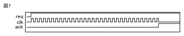
- FIG. 7 is a transition diagram of signals in the circuit of FIG. 6.
- FIG. 13 illustrates an asynchronous circuit according to a second embodiment.
- FIG. 13 is a diagram for explaining an operation of comparing a value of a binary counter with a predetermined value "7.”
- FIG. 11 is a diagram for explaining an operation of comparing a value of a Gray code counter with a predetermined value "7.”
- FIG. 11 is a diagram for explaining delay adjustment by a second delay adjustment circuit 212.
- FIG. 13 is a diagram for explaining an example of a case where there is no delay adjustment by the third delay adjustment circuit 213.
- FIG. 11 is a diagram for explaining delay adjustment by a third delay adjustment circuit 213.
- FIG. FIG. 13 is a diagram illustrating an asynchronous circuit according to a third embodiment.
- FIG. 1 is a diagram for explaining data capture in a conventional SPI communication interface.
- FIG. 1 is a diagram for explaining data capture in a conventional SPI communication interface.
- FIG. 13 is a diagram for explaining data capture in an interface 302 according to the third embodiment.
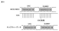
- FIG. 13 is a diagram for explaining CRC processing in the interface 302 of the third embodiment.
- 13 is a diagram showing the format of data transmitted from the master through the MOSI signal line.
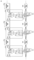
- FIG. 1 is a diagram showing an asynchronous circuit according to a reference example.
- the propagation delay between register groups RG1, RG2, ... is managed using CL (ClickElement) 1, CL2, ....
- CL ClickElement
- the skew adjustment includes the propagation delay (max, min) of the clock path, the propagation delay (max, min) of the data path, the setup time of register groups RG1, RG2, ..., and the hold time of RG1, RG2, .... It is necessary to satisfy the timing requirements of all the joining data, and the delay adjustment is performed by inserting delay adjustment circuits DL1, DL2, ... between CL1, CL2, ..., etc.
- This method is not a problem for pipeline processing where data flows in a fixed direction, but when a value from a later stage of the pipeline is used in a previous stage, or when processing results from other CLs (ClickElements) are merged, delay adjustments become more complex and design becomes more difficult.
- FIG. 2 is a conceptual diagram of a clock generating circuit 220 included in the control circuit of the asynchronous circuit according to the first embodiment.
- the clock generating circuit 220 outputs a clock clk with an expandable pulse width.
- the clock generating circuit 220 includes a control unit 201 and an oscillator 202.
- the control unit 201 receives a request signal req and an acknowledgment signal ack from the outside.
- the control unit 201 sets the drive signal that drives the oscillator 202 to a high level only when the request signal req is activated (high level) and the acknowledgment signal ack is inactivated (low level).
- the oscillator 202 outputs the clock clk to the outside only when the drive signal from the control unit 201 is at a high level.
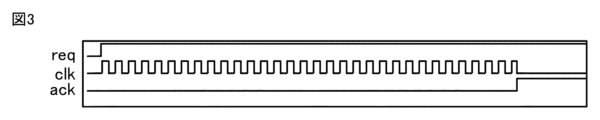
- FIG. 3 is a transition diagram of signals in the circuit of FIG.
- control unit 201 sets the drive signal to high level.
- the oscillator 202 outputs a clock clk.
- the control unit 201 sets the drive signal to low level.
- the oscillator 202 stops outputting the clock clk. After the acknowledgement signal ack goes high level, all signals in the asynchronous circuit are inactivated, so no dynamic power consumption occurs. All signals include data signals, control signals (including reset signals, enable signals, select signals, etc.), address signals, data bus signals, and interrupt signals.
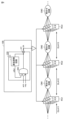
- FIG. 4 illustrates an asynchronous circuit according to the first embodiment.
- the asynchronous circuit includes register groups RG1, RG2, . . . , combinational circuits CM1, CM2, .
- the clock clk is used to control the flow of data within the digital circuit and ensure data stability and timing.
- the clock clk is supplied to the register groups RG1, RG2, ...
- Each of the register groups RG1, RG2, ... has at least one register.
- Data is read from and written to the register groups RG1, RG2, ... in synchronization with the rising or falling edge of the clock clk (or a specific clock cycle).
- the clock clk prevents data inconsistencies and conflicts and ensures signal timing.
- the clock clk propagates the data in the register groups RG1, RG2, ... to the combinational circuits CM1, CM2, .... This ensures signal synchronization and reliability, and allows accurate data processing.
- Combinational circuits CM1, CM2, ... are a type of digital circuit that immediately generates an output signal from an input signal.
- the operation of combinational circuits CM1, CM2, ... does not depend on timing information such as the clock (clk), because they apply a specific logic function to the input and generate an output.
- the combinational circuits CM1, CM2, . . . carry out the following processes.
- Combinational circuits CM1, CM2, ... apply a pre-designed logic function to the input signals. This function generates an output for each input combination.
- Logic functions are constructed using basic logic gates (AND, OR, NOT, etc.) to calculate the output according to the combination conditions.
- the combinational circuits CM1, CM2, ... generate output signals calculated based on logic functions. These output signals are supplied to other components in the digital circuit or to external devices depending on the purpose of the combinational circuits.
- Combinational circuits CM1, CM2, ... are composed of logic gates, decoders, encoders, multiplexers, arithmetic logic units (ALUs), etc. These circuits are important in data processing and control, and are fundamental elements of logic design and digital circuits.
- the asynchronous circuit of the first embodiment includes a control circuit 100 instead of CL1, CL2, ... and delay adjustment circuits DL1, DL2, ... included in the asynchronous circuit of the reference example.
- the control circuit 100 of the asynchronous circuit in FIG. 4 includes a clock generation circuit 220 that outputs a clock clk with an expandable pulse width.
- the clock generation circuit 220 includes a delay adjustment circuit 101 and an AND circuit 205.
- the AND circuit 205 and the delay adjustment circuit 101 in FIG. 4 are circuits that embody the control unit 201 and the oscillator 202 in FIG. 2.
- the delay adjustment circuit 101 outputs a delayed clock clkd, which is the clock clk output from the AND circuit 205 delayed by a delay amount d.
- the AND circuit 205 outputs the logical product of the request signal req, the inverted signal of the acknowledgement signal ack, and the inverted signal of the delayed clock clkd as the clock clk.
- the clock clk output from the clock generation circuit 220 is supplied to the register groups RG1, RG2, ....
- the register groups RG1, RG2, ... output the data they hold to the subsequent combinational circuits CM1, CM2, ... at the timing of the rising edge of the clock clk.
- CTS Lock Tree Synthesis
- a clock signal is generated for use within a digital circuit. This clock signal must be synchronized with all parts of the digital circuit.
- Minimizing delays Minimizing delays in the clock signal within the circuit and designing it to meet timing requirements, thereby ensuring accurate processing of data signals.
- Logic Synthesis is the first step in digital design. It involves generating a gate-level logic circuit from a logic description (usually written in an HDL language). Designers translate the design from a high-level synthesis language into a set of concrete gates and flip-flops, and evaluate the quality and performance of the design at this stage.
- Post-synthesis layout generation generates the placement and connection information of actual transistors and wiring based on the synthesized logic circuit. At this stage, the physical shape and size of the circuit are determined.
- (D) Clock Tree Design Design the clock tree. This involves planning the propagation path of the clock signal from the source of the clock signal (usually a clock generator) to each part and designing a method to distribute the clock signal evenly.
- Timing Analysis and Optimization Once the clock tree design and wiring routing are complete, timing analysis such as Static Timing Analysis (STA) is performed and optimization is performed if necessary to ensure that the timing requirements of the clock signal are met.
- STA Static Timing Analysis
- delay Adjustment In the reference example, a plurality of delay adjustment circuits are required, whereas in this embodiment, delay adjustment can be performed with only one delay adjustment circuit.
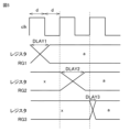
- Figure 5 shows the clock clk and the transition of data in the registers in each of the register groups RG1, RG2, and RG3.
- the data delays DLAY1, DLAY2, and DLAY3 are the processing times of the combinational circuits CM0 (not shown), CM1, and CM2.
- One cycle of clk is generated by the signal circulating twice through the closed loop formed by the delay adjustment circuit 101 and the AND circuit 205.
- the high level period and low level period of clk are the delay amount d of the delay adjustment circuit 101.
- the delay amount d of the delay adjustment is adjusted to match the maximum data delay DMAX among the data delays DLAY1, DLAY2, ... based on the STA results (satisfying the setup constraints and hold constraints).
- DMAX DLAY2.
- the number of places where delay adjustment specific to asynchronous design is performed can be reduced (to one place), so that the power consumption of the asynchronous circuit can be reduced.
- the asynchronous circuit and the control circuit for the asynchronous circuit according to this embodiment are suitable for large-scale circuits.
- Embodiment 2 In pipeline processing, the number of cycles from the occurrence of a request (activation of a request signal req) to the completion of processing is often known. In such a case, it is possible to generate an acknowledgement signal ack inside the control circuit of the asynchronous control circuit.
- the control circuit of the asynchronous circuit of this embodiment has a function of generating an acknowledgement signal ack.
- FIG. 6 is a conceptual diagram of a control circuit 200 of an asynchronous circuit according to the second embodiment.
- the control circuit 200 of the asynchronous circuit includes a clock generating circuit 220 that outputs a clock clk having an expandable pulse width, a counter 203, and a comparator 204.
- the clock generating circuit 220 includes a control unit 201 and an oscillator 202.
- the control unit 201 receives a request signal req from the outside and receives an acknowledgment signal ack from the comparator 204.
- the control unit 201 sets the drive signal that drives the oscillator 202 to a high level only when the request signal req is activated (high level) and the acknowledgment signal ack is inactivated (low level).
- the oscillator 202 outputs the clock clk to the counter 203 and to the outside only when the drive signal from the control unit 201 is at a high level.
- the counter 203 counts the number of pulses of the clock clk output from the oscillator 202.
- the counter 203 outputs the number of pulses of the clock clk as a counter value.
- the counter 203 receives a request signal req.
- the counter 203 resets the counter value to 0 when the request signal req rises to a high level.
- the comparator 204 compares the counter value (the number of pulses of the clock clk) output from the counter 203 with a predetermined number of times, and outputs an acknowledgement signal ack based on the comparison result to the outside and the control unit 201.
- the comparator 204 sets the acknowledgement signal ack to inactive (low level) when the counter value is less than a predetermined number, and sets the acknowledgement signal ack to active (high level) when the counter value is equal to the predetermined number.
- FIG. 7 is a transition diagram of signals in the circuit of FIG.
- control unit 201 sets the drive signal to a high level, and the counter 203 resets the count value to "0".
- the oscillator 202 outputs a clock clk.
- the counter 203 counts the number of pulses of the clock clk and outputs the number of pulses of the clock clk as a counter value.
- the comparator 204 sets the acknowledgement signal ack to a high level when the counter value is equal to a predetermined number of times.
- the control unit 201 stops outputting the clock clk. After the acknowledgement signal ack becomes a high level, all signals in the asynchronous circuit are inactivated, so no dynamic power consumption is generated.
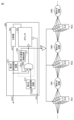
- FIG. 8 shows an asynchronous circuit according to a second embodiment.
- the asynchronous circuit according to the second embodiment includes a control circuit 200 instead of the control circuit 100 according to the first embodiment.
- the control circuit 200 of the asynchronous circuit includes a clock generation circuit 220 that outputs a clock clk with an expandable pulse width, a counter 203, a comparator 204, a second delay adjustment circuit 212, and a third delay adjustment circuit 213.
- the clock generation circuit 220 includes a first delay adjustment circuit 211 and an AND circuit 205.
- the AND circuit 205 and the first delay adjustment circuit 211 in FIG. 8 are circuits that embody the control unit 201 and oscillator 202 in FIG. 6.
- the AND circuit outputs the logical product of the delayed request signal reqd, the inverted signal of the delayed acknowledgement signal ackd, and the inverted signal of the delayed clock clkd as the clock clk.
- the clock clk output from the clock generation circuit 220 is supplied to the register groups RG1, RG2, ....
- the counter 203 counts the number of pulses of the clock clk output from the clock generating circuit 220.
- the counter 203 outputs the number of pulses of the clock clk as a counter value.
- the counter 203 is configured as a Gray code counter.
- the request signal req is input to the reset terminal of the counter 203.
- the counter 203 resets the counter value to 0 in response to the request signal req rising to a high level.
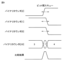
- FIG. 9 is a diagram for explaining the operation of comparing the value of a binary counter with a predetermined value "7".
- a binary counter When a binary counter is used, glitches may occur due to skew between bits. For this reason, restrictions are imposed, such as limiting the value given to the comparator 204 to a power of 2.
- FIG. 10 is a diagram for explaining the operation of comparing the value of the Gray code counter with a predetermined value of "7."
- the first delay adjustment circuit 211 delays the clock clk output from the AND circuit 205 by a first delay amount d1 and inputs the delayed clock clk to the AND circuit 205.
- the first delay adjustment circuit 211 is similar to the delay adjustment circuit of the first embodiment. Therefore, the first delay amount d1 is the same as the delay amount d described in the first embodiment.
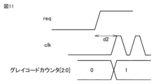
- FIG. 11 is a diagram for explaining the delay adjustment by the second delay adjustment circuit 212.
- the second delay adjustment circuit 212 outputs a delayed request signal reqd, which is obtained by delaying the request signal req by a second delay amount d2, to the clock generation circuit 220.
- the second delay amount d2 is set to be equal to or greater than the removal time of the counter 203.
- the clock generation circuit 220 starts outputting the clock clk.
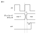
- FIG. 12 is a diagram for explaining an example of a case where there is no delay adjustment by the third delay adjustment circuit 213.
- FIG. 12 is a diagram for explaining an example of a case where there is no delay adjustment by the third delay adjustment circuit 213.
- the clock generation circuit 220 stops generating the clock clk and sets the clock clk to low level. This shortens the pulse width of the clock clk, and part of the clock clk is missing.
- FIG. 13 is a diagram for explaining the delay adjustment by the third delay adjustment circuit 213.
- the third delay adjustment circuit 213 outputs a delayed acknowledgement signal ackd, which is obtained by delaying the acknowledgement signal ack output from the comparator 204 by a third delay amount d3, to the outside and to the clock generation circuit 2220.
- the clock generation circuit 220 stops generating the clock clk and sets the clock clk to a low level. In order to prevent any dropout of the clock clk (to guarantee a minimum pulse width), the following conditions must be satisfied between the first delay amount d1, the third delay amount d3, and the processing time dA by the counter 203 and the comparator 204.
- the number of places where delay adjustment specific to asynchronous design is performed can be reduced (to three places), so that the power consumption of the asynchronous circuit can be reduced.
- the asynchronous circuit and the control circuit for the asynchronous circuit according to this embodiment are suitable for large-scale circuits.
- Embodiment 3. 14 is a diagram showing an asynchronous circuit according to embodiment 3.
- the asynchronous circuit is a slave that communicates with an external master.
- the asynchronous circuit includes a control circuit 200, an interface 302, a register 303, a buffer 304, an AD converter 305, and a sensor 306.
- the control circuit 200 is similar to the control circuit 200 of the second embodiment.
- the control circuit 200 is configured to supply a clock clk to the AD converter 305 and the buffer 304, receive a request signal req from the register 303, and output a delayed acknowledgement signal ackd to the register 303.
- Serial Peripheral Interface 302 is a Serial Peripheral Interface (SPI) that communicates with an external master.
- SPI Serial Peripheral Interface
- the register 303 is connected to the interface 302.
- the register 303 outputs a request signal req to the control circuit 200, and receives a delayed acknowledgement signal ackd output from the control circuit 200.
- the register 303 outputs a start instruction signal to the AD converter 305.
- the sensor 306 outputs analog data representing the detection result to the AD converter 305 .
- the AD converter 305 converts analog data from the sensor 306 into digital data and outputs the digital data to the buffer 304 .
- the buffer 304 stores the digital data output from the AD converter 305 when the clock clk is supplied.
- the interface 302 causes the register 303 to output a signal instructing the AD converter 305 to start, and also causes the register 303 to output an activated request signal req.
- the AD converter 305 and buffer 304 do not operate because they are not being supplied with clk.
- control circuit 200 When the control circuit 200 receives an activated request signal req, it starts supplying the clock clk to the AD converter 305 and the buffer 304.
- the AD converter 305 and buffer 304 start operating as they receive the clock clk, and the AD converter 305 converts the analog data from the sensor 306 into digital data and outputs it to the buffer 304.
- the control circuit 200 activates the acknowledgement signal ack and stops the supply of the clock clk.
- the AD converter 305 and buffer 304 stop operating because they are not supplied with the clock clk.
- Interface 302 reads the state of the delayed acknowledgement signal ackd stored in register 303 at any timing according to an instruction signal included in the data received by SPI communication from the master. When register 303 receives an activated delayed acknowledgement signal ackd, interface 302 reads data from buffer 304.
- the interface 302 It is desirable for the interface 302 to minimize dynamic power consumption during standby, so by selecting the SPI protocol, which stops the clock, further reductions in power consumption during standby can be expected.
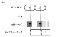
- Figure 15 is a diagram to explain data capture in a conventional SPI communication interface.
- the interface receives the edge of the serial clock SCK synchronously with the internal clock clk.
- the interface captures the data on the MOSI (Master Out Slav In) signal line at the edge of the next pulse of the internal clock clk that has been received synchronously.
- MOSI Master Out Slav In
- the internal clock clk must be constantly running, which is not suitable for power saving.
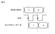
- FIG. 16 is a diagram for explaining data capture in the interface 302 of embodiment 3.
- Interface 302 simultaneously receives data from the MOSI signal line and the serial clock SCK from the clock signal line.
- Interface 302 captures data on the MOSI signal line at the edge of the serial clock SCK.
- the internal clock clk does not need to be constantly running, which can reduce power consumption.
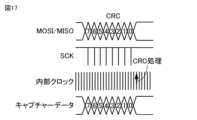
- Figure 17 is a diagram to explain CRC (Cyclic Redundancy Check) processing in a conventional SPI communication interface.
- CRC Cyclic Redundancy Check
- the interface After completing reception of data from the MOSI signal line, the interface executes CRC processing of the capture data using the internal clock clk, and outputs the processing result to register 303.
- the interface 302 uses the serial clock SCK instead of the internal clock clk, but in SPI communication, the serial clock SCK is not supplied after data transmission and reception is completed. This causes a problem in that a clock cannot be obtained for CRC processing of the capture data.
- FIG. 18 is a diagram for explaining CRC processing in the interface 302 of the third embodiment.
- FIG. 19 is a diagram showing the format of data transmitted from the master through the MOSI signal line.
- the master After transmitting one byte of CRC data, the master transmits one byte of dummy data via the MOSI signal line and the serial clock SCK via the clock signal line.
- the interface 302 simultaneously receives the one byte of dummy data from the MOSI signal line and the serial clock SCK from the clock signal line.
- the interface 302 performs CRC processing on the captured data based on the serial clock SCK and outputs the processing result to the register 303.
Landscapes
- Engineering & Computer Science (AREA)
- Software Systems (AREA)
- Theoretical Computer Science (AREA)
- Computer Networks & Wireless Communication (AREA)
- Signal Processing (AREA)
- Physics & Mathematics (AREA)
- General Engineering & Computer Science (AREA)
- General Physics & Mathematics (AREA)
- Logic Circuits (AREA)
Priority Applications (3)
| Application Number | Priority Date | Filing Date | Title |
|---|---|---|---|
| PCT/JP2023/043450 WO2025120727A1 (ja) | 2023-12-05 | 2023-12-05 | 非同期回路の制御回路および非同期回路 |
| JP2025561705A JPWO2025120961A1 (cg-RX-API-DMAC7.html) | 2023-12-05 | 2024-09-20 | |
| PCT/JP2024/033630 WO2025120961A1 (ja) | 2023-12-05 | 2024-09-20 | 非同期回路の制御回路、非同期回路および非同期回路の設計方法 |
Applications Claiming Priority (1)
| Application Number | Priority Date | Filing Date | Title |
|---|---|---|---|
| PCT/JP2023/043450 WO2025120727A1 (ja) | 2023-12-05 | 2023-12-05 | 非同期回路の制御回路および非同期回路 |
Publications (1)
| Publication Number | Publication Date |
|---|---|
| WO2025120727A1 true WO2025120727A1 (ja) | 2025-06-12 |
Family
ID=95979600
Family Applications (2)
| Application Number | Title | Priority Date | Filing Date |
|---|---|---|---|
| PCT/JP2023/043450 Pending WO2025120727A1 (ja) | 2023-12-05 | 2023-12-05 | 非同期回路の制御回路および非同期回路 |
| PCT/JP2024/033630 Pending WO2025120961A1 (ja) | 2023-12-05 | 2024-09-20 | 非同期回路の制御回路、非同期回路および非同期回路の設計方法 |
Family Applications After (1)
| Application Number | Title | Priority Date | Filing Date |
|---|---|---|---|
| PCT/JP2024/033630 Pending WO2025120961A1 (ja) | 2023-12-05 | 2024-09-20 | 非同期回路の制御回路、非同期回路および非同期回路の設計方法 |
Country Status (2)
| Country | Link |
|---|---|
| JP (1) | JPWO2025120961A1 (cg-RX-API-DMAC7.html) |
| WO (2) | WO2025120727A1 (cg-RX-API-DMAC7.html) |
Citations (2)
| Publication number | Priority date | Publication date | Assignee | Title |
|---|---|---|---|---|
| JP2003058271A (ja) * | 2001-08-15 | 2003-02-28 | Fujitsu Ltd | 半導体装置及びクロック制御方法 |
| US20060161797A1 (en) * | 2003-01-24 | 2006-07-20 | Eckhard Grass | Asynchronous wrapper for a globally asynchronous, locally synchronous (gals) circuit |
Family Cites Families (1)
| Publication number | Priority date | Publication date | Assignee | Title |
|---|---|---|---|---|
| JP5533119B2 (ja) * | 2010-03-25 | 2014-06-25 | 富士通株式会社 | レイアウト設計装置、レイアウト設計方法、及びレイアウト設計プログラム |
-
2023
- 2023-12-05 WO PCT/JP2023/043450 patent/WO2025120727A1/ja active Pending
-
2024
- 2024-09-20 JP JP2025561705A patent/JPWO2025120961A1/ja active Pending
- 2024-09-20 WO PCT/JP2024/033630 patent/WO2025120961A1/ja active Pending
Patent Citations (2)
| Publication number | Priority date | Publication date | Assignee | Title |
|---|---|---|---|---|
| JP2003058271A (ja) * | 2001-08-15 | 2003-02-28 | Fujitsu Ltd | 半導体装置及びクロック制御方法 |
| US20060161797A1 (en) * | 2003-01-24 | 2006-07-20 | Eckhard Grass | Asynchronous wrapper for a globally asynchronous, locally synchronous (gals) circuit |
Also Published As
| Publication number | Publication date |
|---|---|
| WO2025120961A1 (ja) | 2025-06-12 |
| JPWO2025120961A1 (cg-RX-API-DMAC7.html) | 2025-06-12 |
Similar Documents
| Publication | Publication Date | Title |
|---|---|---|
| Bormann et al. | Asnchronous Wrapper for Heterogeneous Systems. | |
| Mullins et al. | Demystifying data-driven and pausible clocking schemes | |
| US20090115469A1 (en) | Variability-Aware Scheme for Asynchronous Circuit Initialization | |
| US10084434B2 (en) | Relative timed clock gating cell | |
| US5306962A (en) | Qualified non-overlapping clock generator to provide control lines with non-overlapping clock timing | |
| US7500205B2 (en) | Skew reduction for generated clocks | |
| WO2023279341A1 (zh) | 用于设计异步电路的方法和电子设备 | |
| Pontes et al. | SCAFFI: An intrachip FPGA asynchronous interface based on hard macros | |
| JP5120785B2 (ja) | 非同期式論理回路の論理回路設計装置、論理回路設計方法および論理回路設計プログラム | |
| JP3488224B2 (ja) | 遷移信号制御装置とそれを用いたdmaコントローラ及び遷移信号制御プロセッサ | |
| JP2579237B2 (ja) | フロースルーラッチ回路を有する状態素子回路、該状態素子回路を有するvlsi回路、及びラッチをマスタースレーブフリップフロップの機能的代替物として作動する方法 | |
| JPH10134091A (ja) | 論理エミュレーションの最適化回路生成法 | |
| JP2000341093A (ja) | 低消費電力ディジタル論理回路 | |
| WO2024243770A1 (zh) | 异步电路、其实现方法、芯片、介质、产品及电子设备 | |
| JP2002524790A (ja) | 同期多相クロック分配システム | |
| WO2025120961A1 (ja) | 非同期回路の制御回路、非同期回路および非同期回路の設計方法 | |
| JPH10133768A (ja) | クロックシステム、半導体装置、半導体装置のテスト方法、及びcad装置 | |
| CN117648894A (zh) | 一种轻量级异步控制器电路及时序控制方法 | |
| CN117313592A (zh) | 一种频率自适应的异步电路及其约束方法 | |
| US7380153B2 (en) | Micropipeline stage controller and control scheme | |
| US5828872A (en) | Implementation of high speed synchronous state machines with short setup and hold time signals | |
| Agiwal et al. | An architecture and a wrapper synthesis approach for multi-clock latency-insensitive systems | |
| Singh et al. | Generalized latency-insensitive systems for gals architectures | |
| JP2004326222A (ja) | データ処理システム | |
| JP2000353939A (ja) | クロック信号同期式フリップフロップ回路 |
Legal Events
| Date | Code | Title | Description |
|---|---|---|---|
| 121 | Ep: the epo has been informed by wipo that ep was designated in this application |
Ref document number: 23960742 Country of ref document: EP Kind code of ref document: A1 |
|
| NENP | Non-entry into the national phase |
Ref country code: DE |