WO2025115604A1 - 固体電解コンデンサの製造方法 - Google Patents
固体電解コンデンサの製造方法 Download PDFInfo
- Publication number
- WO2025115604A1 WO2025115604A1 PCT/JP2024/040243 JP2024040243W WO2025115604A1 WO 2025115604 A1 WO2025115604 A1 WO 2025115604A1 JP 2024040243 W JP2024040243 W JP 2024040243W WO 2025115604 A1 WO2025115604 A1 WO 2025115604A1
- Authority
- WO
- WIPO (PCT)
- Prior art keywords
- region
- layer
- water
- electrolytic capacitor
- masking
- Prior art date
- Legal status (The legal status is an assumption and is not a legal conclusion. Google has not performed a legal analysis and makes no representation as to the accuracy of the status listed.)
- Pending
Links
Images









Classifications
-
- H—ELECTRICITY
- H01—ELECTRIC ELEMENTS
- H01G—CAPACITORS; CAPACITORS, RECTIFIERS, DETECTORS, SWITCHING DEVICES, LIGHT-SENSITIVE OR TEMPERATURE-SENSITIVE DEVICES OF THE ELECTROLYTIC TYPE
- H01G9/00—Electrolytic capacitors, rectifiers, detectors, switching devices, light-sensitive or temperature-sensitive devices; Processes of their manufacture
Definitions
- the present invention relates to a method for manufacturing a solid electrolytic capacitor.
- Patent Document 1 discloses a method for producing a solid electrolytic capacitor element by forming a dielectric layer made of an oxide film on the roughened surface of a valve metal substrate, forming a resist layer to separate the anode and cathode sections, and sequentially forming a solid electrolyte layer and a current collecting layer made of a carbon paste layer and a silver paste layer on the dielectric layer excluding the anode section.
- a method for forming a solid electrolyte layer a method using a raw material solution containing a material for forming the solid electrolyte layer is known. Specifically, a method of applying a polymerization solution containing a monomer that will become a solid electrolyte layer by chemical polymerization reaction to form a polymerized film of a conductive polymer on the surface of a dielectric layer, or a method of depositing polymer particles in which a polymerizable monomer is previously polymerized on the surface of a dielectric layer to form a film of a conductive polymer is known.
- the solid electrolytic capacitor element described in Patent Document 1 has a configuration in which an anode portion (hereinafter referred to as an anode terminal region in this specification) and a cathode portion (hereinafter referred to as a cathode formation region in this specification) of a valve metal substrate are separated by providing a resist layer (hereinafter referred to as a masking member in this specification).
- a masking member in this specification, for example, when the raw material liquid is applied to the cathode formation region, the raw material liquid is applied to the surface of the masking member so as to contact the end of the masking member on the cathode formation region side in order to maximize the width of the cathode formation region.
- This raw material liquid tends to wet and spread on the surface of the masking member, and may reach the anode terminal region side beyond the masking member. If the raw material liquid reaches the valve action metal base on the anode terminal region side, there is a risk of LC failure (leakage current failure).
- the present invention has been made to solve the above problems, and aims to provide a method for manufacturing a solid electrolytic capacitor that can prevent the occurrence of LC defects in a method for manufacturing a solid electrolytic capacitor that uses a method of providing a masking member to form a solid electrolyte layer in the cathode formation region.
- the method for manufacturing a solid electrolytic capacitor of the present invention is a method for manufacturing a solid electrolytic capacitor having a solid electrolytic capacitor element having a valve metal substrate having an anode terminal region and a cathode formation region, a dielectric layer formed on the valve metal substrate, a solid electrolyte layer formed on the dielectric layer, and a current collecting layer formed on the solid electrolyte layer, and includes the steps of: forming a masking region made of a masking material on the valve metal substrate to separate the anode terminal region from the cathode formation region and insulate the valve metal substrate from a counter electrode; providing a water-repellent layer on at least a part of the anode side masking region located on the anode terminal region side of the cathode side masking region, without providing a water-repellent layer on the surface of the masking region, which is a predetermined region including the end on the cathode formation region side; and applying a raw material liquid containing a material for forming the
- the present invention provides a method for manufacturing a solid electrolytic capacitor that can prevent the occurrence of LC defects in a method for manufacturing a solid electrolytic capacitor that uses a method of forming a solid electrolyte layer in a cathode formation region by providing a masking member.
- FIG. 1 is a cross-sectional view illustrating a schematic example of a solid electrolytic capacitor element.
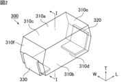
- FIG. 2 is a perspective view that illustrates a schematic diagram of an example of a solid electrolytic capacitor including the solid electrolytic capacitor element shown in FIG.
- FIG. 3 is a cross-sectional view of the solid electrolytic capacitor shown in FIG. 2 taken along line II.
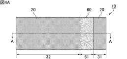
- FIG. 4A is a plan view showing a schematic example of a valve metal substrate on which a dielectric layer and a masking region are formed.
- FIG. 4B is a cross-sectional view taken along line AA of FIG. 4A.
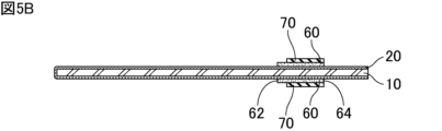
- FIG. 5A is a plan view that illustrates an example of an element provided with a water-repellent layer.
- FIG. 5A is a plan view that illustrates an example of an element provided with a water-repellent layer.
- FIG. 5B is a cross-sectional view taken along line BB in FIG. 5A.
- FIG. 6 is a cross-sectional view showing a schematic example of an element in which a solid electrolyte layer is formed.
- FIG. 7 is a cross-sectional view showing a schematic example of an element on which a conductive layer is formed.
- FIG. 8 is a cross-sectional view illustrating a schematic diagram of another example of an element provided with a water-repellent layer.
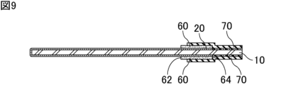
- FIG. 9 is a cross-sectional view that illustrates a schematic diagram of another example of an element provided with a water-repellent layer.
- FIG. 10 is a cross-sectional view that shows a schematic example of a state in which a solid electrolyte layer and a current collecting layer are formed on the element shown in FIG. 9 and the water-repellent layer is peeled off.
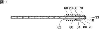
- FIG. 11 is a cross-sectional view that illustrates an example of an element provided with an acrylic resin layer and a water-repellent layer.
- FIG. 12 is a cross-sectional view that shows a schematic example of a state in which a solid electrolyte layer and a current collecting layer are formed on the element shown in FIG. 11, and the acrylic resin layer and the water-repellent layer are peeled off.
- FIG. 13 is a cross-sectional view that illustrates another example of an element provided with an acrylic resin layer and a water-repellent layer.
- the method for producing the solid electrolytic capacitor of the present invention will now be described. First, an example of the configuration of a solid electrolytic capacitor that is an object to be manufactured by the manufacturing method of a solid electrolytic capacitor of the present invention and the configuration of a solid electrolytic capacitor element that constitutes the solid electrolytic capacitor will be described. Note that the object to be manufactured by the manufacturing method of a solid electrolytic capacitor of the present invention is not limited to the solid electrolytic capacitor and solid electrolytic capacitor element described below.
- present invention is not limited to the configurations below, and can be modified as appropriate within the scope of the present invention. Note that the present invention also includes a combination of two or more of the individual desirable configurations described below.
- FIG. 1 is a cross-sectional view illustrating a schematic example of a solid electrolytic capacitor element.
- the solid electrolytic capacitor element 1 shown in FIG. 1 has a valve metal base 10, a dielectric layer 20 formed on the valve metal base 10, a solid electrolyte layer 40 formed on the dielectric layer 20, and a current collecting layer 50 formed on the solid electrolyte layer 40.
- a masking region 61 made of a masking member 60 is provided on the dielectric layer 20 to separate the anode terminal region 31 and the cathode formation region 32 and to insulate the valve metal substrate 10 from the counter electrode. 1 , three regions are indicated by double-headed arrows: anode terminal region 31, masking region 61, and cathode formation region 32. With masking region 61 as the boundary, the side of anode end 33 where solid electrolyte layer 40 is not provided is defined as anode terminal region 31, and the side of cathode end 34 where solid electrolyte layer 40 is provided is defined as cathode formation region 32.
- the valve metal substrate 10 is made of a valve metal such as an elemental metal such as aluminum, tantalum, niobium, titanium, or zirconium, or an alloy containing these metals.
- the main surface of the valve metal base 10 is preferably porous having pores. By making the main surface of the valve metal base 10 porous, the surface area of the valve metal base 10 is increased. Note that the valve metal base 10 is not limited to a case where both the front and back surfaces are porous, and only one of the front and back surfaces of the valve metal base 10 may be porous.
- the dielectric layer 20 is preferably made of an oxide film provided on the surface of the valve metal substrate.
- the dielectric layer 20 is preferably made of an oxide of aluminum.
- the oxide of aluminum is formed by anodizing the surface of the valve metal substrate 10, as described below.
- a masking region 61 made of a masking member 60 is provided on the valve metal substrate 10.
- the masking member 60 is preferably provided so as to fill a plurality of pores (recesses) of the porous valve metal substrate 10.
- the masking member 60 is formed by applying a masking material such as a composition containing an insulating resin.
- insulating resins include polyphenylsulfone (PPS), polyethersulfone (PES), cyanate ester resin, fluororesin (tetrafluoroethylene, tetrafluoroethylene-perfluoroalkylvinylether copolymer, etc.), a composition consisting of soluble polyimidesiloxane and epoxy resin, polyimide resin, polyamideimide resin, and derivatives or precursors thereof.
- the solid electrolyte layer 40 is provided on the dielectric layer 20 in the cathode formation region 32.
- the solid electrolyte layer 40 is preferably provided so as to fill multiple pores (recesses) of the porous valve metal substrate 10.
- Materials for forming the solid electrolyte layer 40 include conductive polymers such as polypyrroles, polythiophenes, and polyanilines. Among these, polythiophenes are preferred, and poly(3,4-ethylenedioxythiophene), also known as PEDOT, is particularly preferred.
- the conductive polymers may also contain dopants such as polystyrene sulfonate (PSS).
- the solid electrolyte layer 40 is formed by applying a raw material liquid containing a material for forming the solid electrolyte layer 40 so as to cover the cathode formation region partitioned by the masking member 60 .
- the raw material liquid includes a liquid containing a polymerizable monomer, a dispersion of polymer particles in which a polymerizable monomer has been polymerized in advance, and the like. That is, a film of a conductive polymer such as PEDOT-PSS may be formed by using a liquid containing polymerizable monomers such as PEDOT and PSS and polymerizing the monomers on the surface of the dielectric layer 20. Alternatively, a film of a conductive polymer may be formed by depositing polymer fine particles such as PEDOT-PSS in which polymerizable monomers such as PEDOT and PSS have been polymerized in advance on the surface of the dielectric layer 20.
- FIG. 1 shows a carbon layer 51 and a metal layer 52 as the current collecting layer 50.
- the carbon layer 51 can be formed by applying a carbon paste
- the metal layer 52 can be formed by applying a conductive paste such as a silver paste.
- FIG. 2 is a perspective view showing a schematic example of a solid electrolytic capacitor having the solid electrolytic capacitor element shown in FIG. 1.
- FIG. 3 is a cross-sectional view of the solid electrolytic capacitor shown in FIG. 2 taken along line I-I.
- the solid electrolytic capacitor 300 has a generally rectangular parallelepiped outer shape.
- the solid electrolytic capacitor 300 includes an outer casing 310, a first external electrode 320, a second external electrode 330, and a capacitor element assembly 340 including a plurality of solid electrolytic capacitor elements 1.
- the exterior body 310 has a generally rectangular parallelepiped shape. Inside the exterior body 310, a capacitor element assembly 340 including a plurality of solid electrolytic capacitor elements 1 is provided inside the exterior body 310.
- the exterior body 310 has a first main surface 310a and a second main surface 310b that face each other in the height direction T, a first side surface 310c and a second side surface 310d that face each other in the width direction W, and a first end surface 310e and a second end surface 310f that face each other in the length direction L. Note that one solid electrolytic capacitor element 1 may be provided inside the exterior body 310.
- the capacitor element assembly 340 includes a plurality of solid electrolytic capacitor elements 1 (solid electrolytic capacitor element 1a, solid electrolytic capacitor element 1b, solid electrolytic capacitor element 1c, solid electrolytic capacitor element 1d) and a conductive member 319.
- the number of solid electrolytic capacitor elements constituting the capacitor element assembly 340 is four, but the number of solid electrolytic capacitor elements constituting the capacitor element assembly is not particularly limited.
- the multiple solid electrolytic capacitor elements 1 are stacked.
- the multiple solid electrolytic capacitor elements 1 are stacked so that the dimension in the stacking direction on the second end face 310f side is larger than the dimension in the stacking direction on the first end face 310e side.
- the multiple solid electrolytic capacitor elements 1 are arranged so that they spread in the thickness direction from the first end face side toward the second end face side when viewed from the side.
- Each valve metal substrate in the plurality of solid electrolytic capacitor elements 1 is connected to the first external electrode 320 at its anode terminal region. It is preferable that the valve metal substrate is joined by resistance welding at the anode terminal region, and it is preferable that the valve metal substrate is joined to the first external electrode at the anode terminal region by resistance welding.
- the conductive layers of the multiple solid electrolytic capacitor elements 1 are electrically and physically connected by conductive members 319 , which are electrically and physically connected to a second external electrode 330 .
- the conductive member 319 is preferably an electrode paste mainly composed of nickel, silver, or copper, for example. Note that, even if the conductive member 319 is not used, if a conductivity equal to or higher than a desired conductivity is obtained between the solid electrolytic capacitor elements 1, between the solid electrolytic capacitor elements 1b and 1c and the second external electrode 330, etc., the conductive member 319 can be omitted.
- the first external electrode 320 and the second external electrode 330 are preferably formed from a metal material that is easy to bend and has high conductivity.
- the first external electrode 320 and the second external electrode 330 are formed from a material cut out from a metal plate, for example. Note that the first external electrode 320 and the second external electrode 330 may be made of the same material or different materials.
- the exterior body 310 is mainly made of resin and may contain a filler.
- resins include epoxy resin, phenol resin, polyimide resin, silicone resin, polyamide resin, and liquid crystal polymer.
- the resin may be in either solid or liquid form. It is preferred that the corners are rounded by barrel polishing after resin sealing.
- preferred fillers include silica particles, alumina particles, and metal particles. The maximum diameter of the filler is preferably 30 ⁇ m or more and 40 ⁇ m or less. It is more preferred that the material contains silica particles in addition to solid epoxy resin and phenol resin.
- the method for manufacturing a solid electrolytic capacitor of the present invention involves a step of forming a masking region made of a masking material on a valve metal substrate to separate an anode terminal region and a cathode formation region and to insulate the valve metal substrate from a counter electrode.
- FIG. 4A is a plan view showing an example of a valve metal substrate on which a dielectric layer and a masking region are formed
- FIG. 4B is a cross-sectional view taken along line AA of FIG. 4A.
- the valve metal substrate 10 may be a chemically-formed foil having an oxide of aluminum formed thereon as the dielectric layer 20.
- a masking region 61 made of a masking member 60 is provided on the valve metal substrate 10, the masking region 61 is formed on the dielectric layer 20.
- a metal foil not provided with the dielectric layer 20 may be used as the valve metal base 10
- a masking region 61 made of a masking member 60 may be provided on the metal foil, and anodization may be performed to form an oxide film that will become the dielectric layer 20 on the surface of the valve metal base 10.
- the dielectric layer 20 does not exist directly below the masking member 60.
- the method for manufacturing a solid electrolytic capacitor of the present invention includes a step of forming a masking region made of a masking material on a valve metal substrate, whether the masking region is provided on the dielectric layer of a valve metal substrate on which a dielectric layer is provided, or on a valve metal substrate on which no dielectric layer is provided.
- a dielectric layer may or may not be present directly below the masking material.
- the masking area can be formed by applying a solution containing a resin that will become the masking material, and the solution can be applied by methods such as screen printing, roller transfer, dispenser application, inkjet printing, etc.
- the masking region 61 is preferably provided in a strip shape along the lateral direction of the valve metal substrate as shown in FIG. 4A.
- the positions of the anode terminal region 31 and the cathode formation region 32 are determined with the masking region 61 as the boundary.
- the position of the masking region 61 is determined at a position where the area of the cathode formation region 32 is large.
- a water-repellent layer is not provided in the cathode side masking area, which is a predetermined area on the surface of the masking area that includes the end on the cathode formation area side, and a process is performed in which a water-repellent layer is provided in at least a portion of the anode side masking area that is located closer to the anode terminal area than the cathode side masking area.
- FIG. 5A is a plan view that illustrates an example of an element provided with a water-repellent layer
- FIG. 5B is a cross-sectional view taken along line BB of FIG. 5A.
- the water-repellent layer is provided on a part of the surface of the masking region.
- the water-repellent layer 70 is not provided on a cathode-side masking region 63, which is a predetermined region of the surface of the masking region 61 that includes an end 62 on the cathode formation region side, but the water-repellent layer 70 is provided on at least a part of an anode-side masking region 65 located closer to the anode terminal region 31 than the cathode-side masking region 63.
- the water-repellent layer can be formed by applying a solution containing a water-repellent agent. After providing a protective layer on a specific area of the surface of the masking area, including the end on the cathode formation area side, so that the water-repellent agent does not come into contact with the specific area, the solution containing the water-repellent agent is applied to the surface of the masking area.
- the solution can be applied by, for example, screen printing, roller transfer, dispenser application, inkjet printing, or other methods.
- the viscosity of the solution containing the water-repellent agent is preferably higher than the viscosity of the solution containing the resin that will become the masking member.
- the viscosity of the solution containing the resin that will become the masking member is 5 to 15 Pa ⁇ s
- the viscosity of the solution containing the water-repellent agent is preferably 50 to 100 Pa ⁇ s, and more preferably 60 to 90 Pa ⁇ s.
- the water repellent materials such as epoxy resins, polyester resins, silicone, etc. can be used, and it is preferable that the water repellent contains silicone.
- the silicone it is preferable to use a modified silicone in which an appropriate substituent has been introduced to improve water repellency.
- a polymerization liquid containing a monomer that will become a solid electrolyte layer by a chemical polymerization reaction is applied from the cathode formation area to the cathode side masking area of the masking area to form a solid electrolyte layer.
- FIG. 6 is a cross-sectional view showing an example of a device having a solid electrolyte layer formed thereon, the position of which corresponds to the position of FIG. 5B. 6 shows that the solid electrolyte layer 40 is formed on the entire dielectric layer 20 in the cathode formation region 32, and the dielectric layer 20 is not exposed in the cathode formation region 32. The solid electrolyte layer 40 is also formed in the cathode side masking region 63. The solid electrolyte layer 40 is not formed in the anode side masking region 65 and the anode terminal region 31.
- a polymerization liquid containing a monomer that will become the solid electrolyte layer through a chemical polymerization reaction is used.
- the polymerization liquid preferably contains a monomer and a solvent for forming a solid electrolyte layer by a chemical polymerization reaction.
- the conductive polymer constituting the solid electrolyte layer include conductive polymers such as polypyrroles, polythiophenes, polyanilines, etc. Among these, polythiophenes are preferred, and poly(3,4-ethylenedioxythiophene), known as PEDOT, is particularly preferred.
- the monomer contained in the polymerization liquid is preferably a monomer that becomes the above-mentioned conductive polymer by chemical polymerization reaction, and examples of such monomers include pyrrole, thiophene, aniline, etc. Among these, 3,4-ethylenedioxythiophene is more preferable.
- the solvent contained in the polymerization liquid may be an aqueous solvent or an alcohol solvent, and is preferably an alcohol solvent.
- the polymerization liquid may contain an oxidizing agent that acts as a polymerization initiator to polymerize the monomers.
- oxidizing agents include ammonium persulfate, iron p-toluenesulfonate (PTSA), etc.
- the polymerization liquid is applied from the cathode formation region to the cathode-side masking region of the masking region. Specifically, the polymerization liquid is applied so as to straddle the end of the surface of the masking region on the cathode formation region side. In this way, the solid electrolyte layer is reliably formed on the dielectric layer in the cathode formation region.
- the polymerization liquid that has spread from the cathode-side masking region toward the anode terminal region of the masking region is repelled by the water-repellent layer and does not spread to the anode-side masking region, so that the polymerization liquid is prevented from reaching the anode terminal region, thereby preventing LC defects.
- the presence of the cathode side masking area, where no water-repellent layer is provided ensures that a solid electrolyte layer is formed on the dielectric layer in the cathode formation area, and the provision of a water-repellent layer adjacent to the cathode side masking area prevents the polymerization liquid from reaching the anode terminal area.
- the cathode side masking region In order to more reliably form a solid electrolyte layer on the dielectric layer in the cathode formation region, it is preferable to make the cathode side masking region, where no water-repellent layer is provided, wider. On the other hand, in order to more reliably prevent the polymerization solution from reaching the anode terminal region, it is preferable to form the water-repellent layer over a wide area. Thus, for example, it is preferable to make the width of the cathode side masking region 10% or more and less than 100%, assuming that the width of the masking region along the longitudinal direction of the valve metal substrate is 100%.
- drying may be performed as necessary.
- the temperature during drying may be 25°C or higher and 100°C or lower.
- natural drying may be used instead of forced drying using an oven or the like.
- the material may also be left in a semi-dried state.
- FIG. 7 is a cross-sectional view showing a schematic example of an element on which a conductive layer is formed.
- FIG. 7 shows a state in which a current collecting layer 50 (a carbon layer 51 and a metal layer 52 ) is provided on a solid electrolyte layer 40 .
- a carbon paste and a conductive paste are applied onto the solid electrolyte layer to form a carbon layer and a metal layer in predetermined regions, thereby forming a conductive layer.
- the water-repellent layer is preferably peeled off and removed after the formation of the solid electrolyte layer or the conductive layer.
- the method for peeling off the water-repellent layer is not particularly limited, and the water-repellent layer can be physically peeled off.
- a plurality of solid electrolytic capacitor elements are stacked, and the anode terminal area of the valve metal base is joined by a method such as resistance welding, and further joined to a lead frame which serves as a first external electrode.
- the conductive layer on the cathode side is electrically and physically connected by a conductive member, and is also joined to a lead frame that serves as a second external electrode. Then, a capacitor element assembly including a plurality of solid electrolytic capacitor elements is sealed in an exterior body with the first external electrode and the second external electrode extending from the exterior body, thereby obtaining a solid electrolytic capacitor.
- a water-repellent layer is provided in a part of the anode side masking area, and a region of the anode side masking area that is located further toward the anode terminal area than the region where the water-repellent layer is provided is defined as a region of the anode side masking area where the water-repellent layer is not provided.
- FIG. 8 is a cross-sectional view showing a schematic diagram of another example of an element provided with a water-repellent layer, the position of which corresponds to the position of FIG. 5B.
- the water-repellent layer 70 is not provided in a region including the end portion 64 on the anode terminal region side of the surface of the masking region 61. In other words, the water-repellent layer 70 is not provided in a part of the anode side masking region 65.
- the masking region 61 is divided into three regions from the end 62 on the cathode formation region side of the masking region toward the end 64 on the anode terminal region side. That is, it can be said to be divided into a cathode side masking region 63 where the water-repellent layer 70 is not provided, an anode side masking region 65 where the water-repellent layer 70 is provided, and an anode side masking region 65 where the water-repellent layer 70 is not provided, a region 65b.
- the presence of the cathode-side masking region where no water-repellent layer is provided ensures that a solid electrolyte layer is formed on the dielectric layer in the cathode formation region, and the provision of a water-repellent layer adjacent to the cathode-side masking region prevents the polymerization solution from reaching the anode terminal region.
- the method for manufacturing the solid electrolytic capacitor of this embodiment can be carried out by adjusting the area to which the solution containing the water repellent is applied.
- a water-repellent layer is provided on the valve metal substrate in the anode terminal region.
- the step of providing a water-repellent layer on the valve metal substrate includes both the step of providing a water-repellent layer on the dielectric layer of a valve metal substrate having a dielectric layer, and the step of providing a water-repellent layer on a valve metal substrate not having a dielectric layer.
- FIG. 9 is a cross-sectional view showing a schematic diagram of another example of an element provided with a water-repellent layer, the position of which corresponds to the position of FIG. 5B.
- the water-repellent layer 70 is provided continuously from the masking region 61 to the anode terminal region 31. In the anode terminal region 31, the water-repellent layer 70 penetrates into the pores of the valve metal base 10.
- the state in which the water-repellent layer 70 penetrates into the pores of the valve metal base 10 is shown by overlapping the hatching of the water-repellent layer 70 and the hatching of the dielectric layer 20.
- the water-repellent layer is provided over a wide area including the anode terminal area, when the polymerization liquid is applied widely from the cathode formation area to the entire masking area, even if the polymerization liquid comes into contact with the anode terminal area, the solid electrolyte layer is not formed in the anode terminal area, which increases the tolerance for setting conditions for the manufacturing process.
- the water-repellent layer When providing a water-repellent layer in the anode terminal area, the water-repellent layer may be provided over the entire anode terminal area, or it may be provided over only a portion of the anode terminal area. When providing a water-repellent layer over only a portion of the anode terminal area, the water-repellent layer is provided only in a specified area that continues from the masking area. And, no water-repellent layer is provided in the area of the anode terminal area on the anode end side.
- an insulating material such as a water-repellent layer in the anode terminal area can impede resistance welding, but the area where there is no water-repellent layer and the valve metal substrate is exposed is suitable for resistance welding, so this area can be used to perform resistance welding and produce a solid electrolytic capacitor.
- resistance welding of an exposed area of a valve action metal base includes resistance welding of a portion of the valve action metal base where a dielectric layer is provided, and resistance welding of a portion where no dielectric layer is provided. Because the thickness of the dielectric layer is thin, the presence or absence of a dielectric layer has little effect on the workability of resistance welding.
- FIG. 10 is a cross-sectional view that shows a schematic example of a state in which a solid electrolyte layer and a current collecting layer are formed on the element shown in FIG. 9 and the water-repellent layer is peeled off.
- the water-repellent layer 70 When the water-repellent layer 70 is formed on the anode terminal region 31, the water-repellent layer 70 penetrates into the pores of the valve metal base 10 that constitutes the anode terminal region 31.
- the water-repellent layer 70 is peeled off from the surface of the valve metal base 10, parts of the water-repellent layer 70 remain in the pores.
- the state in which parts of the water-repellent layer 70 remain in the pores is shown by overlapping the hatching of the water-repellent layer 70 and the hatching of the dielectric layer 20. Therefore, for solid electrolytic capacitors manufactured by providing a water-repellent layer in the anode terminal region, it is possible to confirm that the solid electrolytic capacitor was manufactured using a water-repellent layer by detecting elements (e.g., Si) derived from the water-repellent agent that constitutes the water-repellent layer through an analytical method such as elemental analysis of the area near the surface of the anode terminal region.
- elements e.g., Si
- the water-repellent layer formed in the masking area does not remain after the water-repellent layer is peeled off, so it is difficult to confirm that a solid electrolytic capacitor was manufactured using a water-repellent layer from a solid electrolytic capacitor manufactured with the water-repellent layer only in the masking area.
- an acrylic resin layer is provided on the valve metal substrate, and a water-repellent layer is also provided on the acrylic resin layer.
- the step of providing an acrylic resin layer on a valve metal base includes both the case where an acrylic resin layer is provided on a dielectric layer of a valve metal base provided with a dielectric layer, and the case where an acrylic resin layer is provided on a valve metal base not provided with a dielectric layer.
- FIG. 11 is a cross-sectional view showing an example of an element provided with an acrylic resin layer and a water-repellent layer, the position of which corresponds to the position of FIG. 5B. 11 , an acrylic resin layer 80 is provided in a part of the anode terminal region 31.
- the water-repellent layer 70 is provided continuously from the masking region 61 onto the acrylic resin layer 80 and over a region of the anode terminal region 31 on the anode end 33 side relative to the acrylic resin layer 80.
- the position where the water-repellent layer is provided is the same as in the third embodiment, so the tolerance for setting the manufacturing process conditions can be increased, just like in the third embodiment.
- FIG. 12 is a cross-sectional view that shows a schematic example of a state in which a solid electrolyte layer and a current collecting layer are formed on the element shown in FIG. 11, and the acrylic resin layer and the water-repellent layer are peeled off.
- the acrylic resin does not penetrate into the pores of the valve metal base constituting the anode terminal region. Therefore, in the area where the acrylic resin layer is peeled off, the acrylic resin layer and the water-repellent layer do not remain in the pores, and the valve metal base is exposed.
- the acrylic resin layer may be provided over the entire anode terminal region.
- 13 is a cross-sectional view showing a schematic diagram of another example of an element provided with an acrylic resin layer and a water-repellent layer, the position of which corresponds to the position of FIG. 5B. 13, an acrylic resin layer 80 is provided over the entire anode terminal region 31.
- the water-repellent layer 70 is provided continuously from the masking region 61 onto the acrylic resin layer 80. After the acrylic resin layer and the water-repellent layer are peeled off, the solid electrolytic capacitor element has a structure as shown in FIG.
- the anode terminal area is an area in which the valve metal substrate is exposed as a whole, and therefore a large area suitable for resistance welding can be obtained. This area can be used to perform resistance welding to produce a solid electrolytic capacitor.
- the present disclosure (1) is a method for manufacturing a solid electrolytic capacitor having a solid electrolytic capacitor element including a valve metal substrate having an anode terminal region and a cathode formation region, a dielectric layer formed on the valve metal substrate, a solid electrolyte layer formed on the dielectric layer, and a current collecting layer formed on the solid electrolyte layer, the method comprising the steps of: forming a masking region made of a masking material on the valve metal substrate to separate the anode terminal region from the cathode formation region and insulate the valve metal substrate from a counter electrode; providing a water-repellent layer on at least a part of the anode side masking region located on the anode terminal region side of the cathode side masking region, without providing a water-repellent layer on the surface of the masking region, which is a predetermined region including the end on the cathode formation region side; and applying a raw material liquid containing a material for forming the solid electrolyte layer from the
- the present disclosure (2) is a method for manufacturing a solid electrolytic capacitor as described in the present disclosure (1), which includes a step of peeling off the water-repellent layer provided on the surface of the masking region after applying the raw material liquid.
- the present disclosure (3) is a method for manufacturing a solid electrolytic capacitor according to the present disclosure (1) or (2), in which the water-repellent layer is provided on a part of the anode-side masking region, and a region of the anode-side masking region that is located further toward the anode terminal region than the region where the water-repellent layer is provided is defined as a region of the anode-side masking region where the water-repellent layer is not provided.
- the present disclosure (4) is a method for manufacturing a solid electrolytic capacitor according to the present disclosure (1) or (2), further comprising providing the water-repellent layer on the valve metal substrate in the anode terminal region.
- the present disclosure (6) is a method for manufacturing a solid electrolytic capacitor according to the present disclosure (1) or (2), further comprising providing an acrylic resin layer on the valve metal substrate in the anode terminal region, and providing the water-repellent layer on the acrylic resin layer.
- the present disclosure (8) is a method for producing a solid electrolytic capacitor according to the present disclosure (6) or (7), which includes a step of peeling off the acrylic resin layer and the water-repellent layer provided on the acrylic resin layer after applying the raw material liquid.
- the present disclosure (9) is a method for manufacturing a solid electrolytic capacitor according to the present disclosure (8), which includes a step of welding a plurality of the solid electrolytic capacitor elements by resistance welding the surface of the valve metal base exposed by peeling off the acrylic resin layer.
Landscapes
- Engineering & Computer Science (AREA)
- Power Engineering (AREA)
- Microelectronics & Electronic Packaging (AREA)
- Fixed Capacitors And Capacitor Manufacturing Machines (AREA)
Abstract
陽極端子領域31と陰極形成領域32とを有する弁作用金属基体10と、弁作用金属基体10上に形成された誘電体層20と、誘電体層20上に形成された固体電解質層40と、固体電解質層40上に形成された集電層50とを有する固体電解コンデンサ素子1を備える固体電解コンデンサ300の製造方法であって、弁作用金属基体10上に、陽極端子領域31と陰極形成領域32とを区画し、弁作用金属基体10を対極と絶縁するための、マスキング部材60からなるマスキング領域61を形成する工程と、マスキング領域61の表面において、陰極形成領域側の端部を含む所定領域である陰極側マスキング領域63には撥水層70を設けず、陰極側マスキング領域63よりも陽極端子領域31側に位置する陽極側マスキング領域65の少なくとも一部に、撥水層70を設ける工程と、固体電解質層40を形成する材料を含有する原料液を、陰極形成領域32からマスキング領域61の陰極側マスキング領域63にわたって付与して固体電解質層40を形成する工程と、を行う、固体電解コンデンサ300の製造方法。
Description
本発明は、固体電解コンデンサの製造方法に関する。
特許文献1には、粗面化された弁作用金属基体の表面に酸化皮膜からなる誘電体層を形成した後、陽極部と陰極部を分断するためにレジスト層を形成し、陽極部を除いた誘電体層上に固体電解質層と、カーボンペースト層及び銀ペースト層からなる集電層とを順次形成する等の方法により固体電解コンデンサ素子を作製する方法が開示されている。
固体電解質層を形成するための方法として、前記固体電解質層を形成する材料を含有する原料液を使用する方法が知られている。具体的には、化学重合反応により固体電解質層となるモノマーを含有する重合液を付与し、誘電体層の表面に導電性高分子の重合膜を形成する方法、または重合性モノマーが予め重合されたポリマー微粒子を誘電体層の表面に堆積させて、導電性高分子の膜を形成する方法等が知られている。
ここで、特許文献1に記載の固体電解コンデンサ素子の構成は、レジスト層(以下、本明細書ではマスキング部材という)を設けることにより弁作用金属基体の陽極部(以下、本明細書では陽極端子領域という)と陰極部(以下、本明細書では陰極形成領域という)を分離した構成である。
このようなマスキング部材を設けた構成において、例えば陰極形成領域に原料液を付与する場合、陰極形成領域を最大限に広くとるためにマスキング部材の陰極形成領域側の端部に接触するように、マスキング部材の表面にまで原料液を付与する。この原料液はマスキング部材の表面に濡れ広がりやすく、マスキング部材を超えて陽極端子領域側にまで到達することがある。そして、陽極端子領域側の弁作用金属基体にまで原料液が到達すると、LC不良(漏れ電流不良)を生じるおそれがあった。
ここで、特許文献1に記載の固体電解コンデンサ素子の構成は、レジスト層(以下、本明細書ではマスキング部材という)を設けることにより弁作用金属基体の陽極部(以下、本明細書では陽極端子領域という)と陰極部(以下、本明細書では陰極形成領域という)を分離した構成である。
このようなマスキング部材を設けた構成において、例えば陰極形成領域に原料液を付与する場合、陰極形成領域を最大限に広くとるためにマスキング部材の陰極形成領域側の端部に接触するように、マスキング部材の表面にまで原料液を付与する。この原料液はマスキング部材の表面に濡れ広がりやすく、マスキング部材を超えて陽極端子領域側にまで到達することがある。そして、陽極端子領域側の弁作用金属基体にまで原料液が到達すると、LC不良(漏れ電流不良)を生じるおそれがあった。
本発明は、上記の問題を解決するためになされたものであり、マスキング部材を設けて陰極形成領域に固体電解質層を形成する方法を用いる固体電解コンデンサの製造方法において、LC不良の発生を防止できる固体電解コンデンサの製造方法を提供することを目的とする。
本発明の固体電解コンデンサの製造方法は、陽極端子領域と陰極形成領域とを有する弁作用金属基体と、前記弁作用金属基体上に形成された誘電体層と、前記誘電体層上に形成された固体電解質層と、前記固体電解質層上に形成された集電層とを有する固体電解コンデンサ素子を備える固体電解コンデンサの製造方法であって、前記弁作用金属基体上に、前記陽極端子領域と前記陰極形成領域とを区画し、前記弁作用金属基体を対極と絶縁するための、マスキング部材からなるマスキング領域を形成する工程と、前記マスキング領域の表面において、前記陰極形成領域側の端部を含む所定領域である陰極側マスキング領域には撥水層を設けず、前記陰極側マスキング領域よりも前記陽極端子領域側に位置する陽極側マスキング領域の少なくとも一部に、撥水層を設ける工程と、前記固体電解質層を形成する材料を含有する原料液を、前記陰極形成領域から前記マスキング領域の前記陰極側マスキング領域にわたって付与して前記固体電解質層を形成する工程と、を行う、固体電解コンデンサの製造方法である。
本発明によれば、マスキング部材を設けて陰極形成領域に固体電解質層を形成する方法を用いる固体電解コンデンサの製造方法において、LC不良の発生を防止できる固体電解コンデンサの製造方法を提供することができる。
以下、本発明の固体電解コンデンサの製造方法について説明する。
はじめに、本発明の固体電解コンデンサの製造方法において製造する対象物である固体電解コンデンサの構成と、固体電解コンデンサを構成する固体電解コンデンサ素子の構成の例について説明する。なお、本発明の固体電解コンデンサの製造方法において製造する対象物は、下記に説明する固体電解コンデンサ及び固体電解コンデンサ素子に限定されるものではない。
はじめに、本発明の固体電解コンデンサの製造方法において製造する対象物である固体電解コンデンサの構成と、固体電解コンデンサを構成する固体電解コンデンサ素子の構成の例について説明する。なお、本発明の固体電解コンデンサの製造方法において製造する対象物は、下記に説明する固体電解コンデンサ及び固体電解コンデンサ素子に限定されるものではない。
また、本発明は、以下の構成に限定されるものではなく、本発明の要旨を変更しない範囲において適宜変更して適用することができる。なお、以下において記載する個々の望ましい構成を2つ以上組み合わせたものもまた本発明である。
図1は、固体電解コンデンサ素子の一例を模式的に示す断面図である。
図1に示す固体電解コンデンサ素子1は、弁作用金属基体10と、弁作用金属基体10上に形成された誘電体層20と、誘電体層20上に形成された固体電解質層40と、固体電解質層40上に形成された集電層50とを有する。
図1に示す固体電解コンデンサ素子1は、弁作用金属基体10と、弁作用金属基体10上に形成された誘電体層20と、誘電体層20上に形成された固体電解質層40と、固体電解質層40上に形成された集電層50とを有する。
固体電解コンデンサ素子1には、誘電体層20上に、陽極端子領域31と陰極形成領域32とを区画し、弁作用金属基体10を対極と絶縁するための、マスキング部材60からなるマスキング領域61が設けられている。
図1には、陽極端子領域31、マスキング領域61、陰極形成領域32の3つの領域をそれぞれ両矢印の範囲で示している。マスキング領域61を境界として、固体電解質層40が設けられない陽極末端33の側を陽極端子領域31とし、固体電解質層40が設けられる陰極末端34の側を陰極形成領域32とする。
図1には、陽極端子領域31、マスキング領域61、陰極形成領域32の3つの領域をそれぞれ両矢印の範囲で示している。マスキング領域61を境界として、固体電解質層40が設けられない陽極末端33の側を陽極端子領域31とし、固体電解質層40が設けられる陰極末端34の側を陰極形成領域32とする。
弁作用金属基体10は、例えば、アルミニウム、タンタル、ニオブ、チタン、ジルコニウム等の金属単体、又は、これらの金属を含む合金等の弁作用金属によって構成されている。
弁作用金属基体10の主面は、細孔を有する多孔質状になっていることが好ましい。弁作用金属基体10の主面が多孔質状になっていることにより、弁作用金属基体10の表面積が大きくなっている。なお、弁作用金属基体10の表面及び裏面の両方が多孔質状である場合に限られず、弁作用金属基体10の表面及び裏面の一方のみが多孔質状であってもよい。
弁作用金属基体10の主面は、細孔を有する多孔質状になっていることが好ましい。弁作用金属基体10の主面が多孔質状になっていることにより、弁作用金属基体10の表面積が大きくなっている。なお、弁作用金属基体10の表面及び裏面の両方が多孔質状である場合に限られず、弁作用金属基体10の表面及び裏面の一方のみが多孔質状であってもよい。
誘電体層20は、上記弁作用金属基体の表面に設けられた酸化被膜によって構成されていることが好ましい。例えば、誘電体層20は、アルミニウムの酸化物で構成されていることが好ましい。アルミニウムの酸化物は、後述するように、弁作用金属基体10の表面が陽極酸化処理されることにより形成される。
マスキング部材60からなるマスキング領域61が弁作用金属基体10上に設けられている。マスキング部材60は、多孔質状になっている弁作用金属基体10の複数の細孔(凹部)を充填するように設けられていることが好ましい。
マスキング部材60は、例えば、絶縁性樹脂を含む組成物などのマスク材を塗布して形成される。絶縁性樹脂としては、例えば、ポリフェニルスルホン(PPS)、ポリエーテルスルホン(PES)、シアン酸エステル樹脂、フッ素樹脂(テトラフルオロエチレン、テトラフルオロエチレン・パーフルオロアルキルビニルエーテル共重合体など)、可溶性ポリイミドシロキサンとエポキシ樹脂からなる組成物、ポリイミド樹脂、ポリアミドイミド樹脂、及び、それらの誘導体又は前駆体等が挙げられる。
固体電解質層40は、陰極形成領域32において誘電体層20上に設けられている。固体電解質層40は、多孔質状になっている弁作用金属基体10の複数の細孔(凹部)を充填するように設けられていることが好ましい。
固体電解質層40を構成する材料としては、例えば、ポリピロール類、ポリチオフェン類、ポリアニリン類等の導電性高分子等が用いられる。これらの中では、ポリチオフェン類が好ましく、PEDOTと呼ばれるポリ(3,4-エチレンジオキシチオフェン)が特に好ましい。また、上記導電性高分子は、ポリスチレンスルホン酸(PSS)等のドーパントを含んでいてもよい。
固体電解質層40は、固体電解質層40を形成する材料を含有する原料液を、マスキング部材60によって区画された陰極形成領域が被覆されるように付与することにより形成される。
ここで、原料液とは、重合性モノマーの含有液、または重合性モノマーが予め重合されたポリマー微粒子の分散液等を含む。
すなわち、例えばPEDOT及びPSS等の重合性モノマーの含有液を用い、誘電体層20の表面で重合させて、PEDOT-PSS等の導電性高分子の膜を形成するようにしてもよい。または、例えばPEDOT及びPSS等の重合性モノマーが予め重合されたPEDOT-PSS等のポリマー微粒子を誘電体層20の表面に堆積させて、導電性高分子の膜を形成するようにしてもよい。
ここで、原料液とは、重合性モノマーの含有液、または重合性モノマーが予め重合されたポリマー微粒子の分散液等を含む。
すなわち、例えばPEDOT及びPSS等の重合性モノマーの含有液を用い、誘電体層20の表面で重合させて、PEDOT-PSS等の導電性高分子の膜を形成するようにしてもよい。または、例えばPEDOT及びPSS等の重合性モノマーが予め重合されたPEDOT-PSS等のポリマー微粒子を誘電体層20の表面に堆積させて、導電性高分子の膜を形成するようにしてもよい。
図1には集電層50としてのカーボン層51及び金属層52を示している。カーボン層51はカーボンペーストの付与により形成することができ、金属層52は銀ペースト等の導電性ペーストの付与により形成することができる。
図2は、図1に示す固体電解コンデンサ素子を備える固体電解コンデンサの一例を模式的に示す斜視図である。図3は、図2に示す固体電解コンデンサのI-I線断面図である。
図2及び図3に示すように、固体電解コンデンサ300は、略直方体状の外形を有している。固体電解コンデンサ300は、外装体310と、第1外部電極320と、第2外部電極330と、複数の固体電解コンデンサ素子1を含むコンデンサ素子集合体340と、を備える。
外装体310は、略直方体状の外形を有している。外装体310の内部には、複数の固体電解コンデンサ素子1を含むコンデンサ素子集合体340が設けられている。外装体310は、高さ方向Tにおいて相対する第1主面310a及び第2主面310b、幅方向Wにおいて相対する第1側面310c及び第2側面310d、並びに、長さ方向Lにおいて相対する第1端面310e及び第2端面310fを有している。なお、外装体310の内部には、1つの固体電解コンデンサ素子1が設けられていてもよい。
コンデンサ素子集合体340は、複数の固体電解コンデンサ素子1(固体電解コンデンサ素子1a、固体電解コンデンサ素子1b、固体電解コンデンサ素子1c、固体電解コンデンサ素子1d)、および、導通部材319を備える。なお、図3に示す形態では、コンデンサ素子集合体340を構成する固体電解コンデンサ素子の個数は4個であるが、コンデンサ素子集合体を構成する固体電解コンデンサ素子の個数は、特に限定されない。
複数の固体電解コンデンサ素子1は、積層されている。この際、複数の固体電解コンデンサ素子1は、第2端面310f側の積層方向の寸法が第1端面310e側の積層方向の寸法よりも大きくなるように積層される。すなわち、複数の固体電解コンデンサ素子1は、側面視して第1端面側から第2端面側に向かって厚み方向に広がるように配置される。
複数の固体電解コンデンサ素子1におけるそれぞれの弁作用金属基体はその陽極端子領域で第1外部電極320に接続される。弁作用金属基体が陽極端子領域で抵抗溶接により接合されていることが好ましく、弁作用金属基体が陽極端子領域で第1外部電極と抵抗溶接により接合されていることが好ましい。
複数の固体電解コンデンサ素子1の導電層は、導通部材319によって電気的物理的に接続され、これらは、第2外部電極330に電気的物理的に接続される。
導通部材319は、例えばニッケル、銀又は銅を主成分とする電極ペーストであることが好ましい。なお、導通部材319を用いなくても、複数の固体電解コンデンサ素子1の間、固体電解コンデンサ素子1b、1cと第2外部電極330との間等で、所望の導電率以上の導電性が得られれば、導通部材319を省略することも可能である。
導通部材319は、例えばニッケル、銀又は銅を主成分とする電極ペーストであることが好ましい。なお、導通部材319を用いなくても、複数の固体電解コンデンサ素子1の間、固体電解コンデンサ素子1b、1cと第2外部電極330との間等で、所望の導電率以上の導電性が得られれば、導通部材319を省略することも可能である。
第1外部電極320及び第2外部電極330は、折り曲げ加工が容易で高い導電性を有する金属材料で形成されていることが好ましい。第1外部電極320及び第2外部電極330は、例えば金属製の板材から切り出された材料で形成されている。なお、第1外部電極320及び第2外部電極330は同一材料であっても良いし、異なる材料であってもよい。
外装体310は、樹脂が主体であり、フィラーを含んでいてもよい。樹脂としては、例えば、エポキシ樹脂、フェノール樹脂、ポリイミド樹脂、シリコーン樹脂、ポリアミド樹脂、液晶ポリマー等が好ましい。樹脂の形態は、固形樹脂、液状樹脂いずれも使用可能である。樹脂封止後のバレル研磨により、角部に丸みが付けられていることが好ましい。フィラーとしては、例えば、シリカ粒子、アルミナ粒子、金属粒子等が好ましい。フィラーの最大径は、例えば30μm以上、40μm以下が望ましい。固形エポキシ樹脂とフェノール樹脂に、シリカ粒子を含む材料であることがより好ましい。
(第1実施形態)
以下に、上記に説明したような固体電解コンデンサ素子を備える固体電解コンデンサを製造する場合を例にして、本発明の固体電解コンデンサの製造方法の実施形態の一例を説明する。
以下に、上記に説明したような固体電解コンデンサ素子を備える固体電解コンデンサを製造する場合を例にして、本発明の固体電解コンデンサの製造方法の実施形態の一例を説明する。
本発明の固体電解コンデンサの製造方法では、弁作用金属基体上に、陽極端子領域と陰極形成領域とを区画し、弁作用金属基体を対極と絶縁するための、マスキング部材からなるマスキング領域を形成する工程を行う。
図4Aは、誘電体層及びマスキング領域が形成された弁作用金属基体の一例を模式的に示す平面図であり、図4Bは、図4AのA-A線断面図である。
弁作用金属基体10としては、誘電体層20としてのアルミニウムの酸化物が形成されている化成箔を用いることができる。この弁作用金属基体10上にマスキング部材60からなるマスキング領域61を設ける場合、マスキング領域61は誘電体層20上に形成される。
また、弁作用金属基体10として誘電体層20が設けられていない金属箔を用い、金属箔上にマスキング部材60からなるマスキング領域61を設けて、陽極酸化処理を行うことにより、弁作用金属基体10の表面に誘電体層20となる酸化被膜を形成してもよい。この場合、マスキング部材60の直下には誘電体層20が存在しない。
弁作用金属基体10としては、誘電体層20としてのアルミニウムの酸化物が形成されている化成箔を用いることができる。この弁作用金属基体10上にマスキング部材60からなるマスキング領域61を設ける場合、マスキング領域61は誘電体層20上に形成される。
また、弁作用金属基体10として誘電体層20が設けられていない金属箔を用い、金属箔上にマスキング部材60からなるマスキング領域61を設けて、陽極酸化処理を行うことにより、弁作用金属基体10の表面に誘電体層20となる酸化被膜を形成してもよい。この場合、マスキング部材60の直下には誘電体層20が存在しない。
本発明の固体電解コンデンサの製造方法では、誘電体層が設けられている弁作用金属基体の誘電体層上にマスキング領域を設ける場合も、誘電体層が設けられていない弁作用金属基体にマスキング領域を設ける場合も、弁作用金属基体上にマスキング部材からなるマスキング領域を形成する工程に含まれる。また、製造される固体電解コンデンサ素子において、マスキング部材の直下には誘電体層が存在していてもよく、存在していなくてもよい。
マスキング領域の形成は、マスキング部材となる樹脂を含む溶液の塗布により行うことができ、溶液の塗布は、例えば、スクリーン印刷、ローラー転写、ディスペンサ塗布、インクジェット印刷等の方法により行うことができる。
マスキング領域61は図4Aに示すように弁作用金属基体の短手方向に沿って帯状に設けることが好ましい。
マスキング領域61を境界として、陽極端子領域31と陰極形成領域32の位置が定まる。通常は、コンデンサの容量を大きくするために、陰極形成領域32の面積が大きくなる位置にマスキング領域61の位置を定める。
マスキング領域61を境界として、陽極端子領域31と陰極形成領域32の位置が定まる。通常は、コンデンサの容量を大きくするために、陰極形成領域32の面積が大きくなる位置にマスキング領域61の位置を定める。
本発明の固体電解コンデンサの製造方法では、マスキング領域の表面において、陰極形成領域側の端部を含む所定領域である陰極側マスキング領域には撥水層を設けず、陰極側マスキング領域よりも陽極端子領域側に位置する陽極側マスキング領域の少なくとも一部に、撥水層を設ける工程を行う。
図5Aは、撥水層が設けられた素子の一例を模式的に示す平面図であり、図5Bは、図5AのB-B線断面図である。
撥水層を設ける工程では、マスキング領域の表面の一部に撥水層を設ける。マスキング領域61の表面のうち、陰極形成領域側の端部62を含む所定領域である陰極側マスキング領域63には撥水層70を設けず、陰極側マスキング領域63よりも陽極端子領域31側に位置する陽極側マスキング領域65の少なくとも一部に撥水層70を設ける。
撥水層を設ける工程では、マスキング領域の表面の一部に撥水層を設ける。マスキング領域61の表面のうち、陰極形成領域側の端部62を含む所定領域である陰極側マスキング領域63には撥水層70を設けず、陰極側マスキング領域63よりも陽極端子領域31側に位置する陽極側マスキング領域65の少なくとも一部に撥水層70を設ける。
マスキング領域の表面において陰極形成領域側の端部を含まない領域に撥水層を設けることによって、撥水層が設けられた領域と撥水層が設けられていない領域が区画される。その結果、陰極形成領域側の端部を含み撥水層が設けられていない領域が、陰極側マスキング領域として定まる。そして、陰極側マスキング領域よりも陽極端子領域側の領域が陽極側マスキング領域として定まる。陽極側マスキング領域において陰極側マスキング領域と隣接する領域は、撥水層が設けられた領域となる。
撥水層70は図5Aに示すように弁作用金属基体の短手方向に沿って帯状に設けることが好ましい。
また、図5A及び図5Bに示す形態では、撥水層70はマスキング領域61の表面のうち、陽極端子領域側の端部64を含む領域に設けられている。すなわち、陽極側マスキング領域65の全体に撥水層70が設けられている。
また、図5A及び図5Bに示す形態では、撥水層70はマスキング領域61の表面のうち、陽極端子領域側の端部64を含む領域に設けられている。すなわち、陽極側マスキング領域65の全体に撥水層70が設けられている。
撥水層の形成は、撥水剤を含む溶液の塗布により行うことができ、マスキング領域の表面のうち陰極形成領域側の端部を含む所定領域に撥水剤が触れないように当該所定領域に保護層を設けたのちに、マスキング領域の表面に撥水剤を含む溶液を塗布する。溶液の塗布は、例えば、スクリーン印刷、ローラー転写、ディスペンサ塗布、インクジェット印刷等の方法により行うことができる。また、撥水剤を含む溶液の粘度は、マスキング部材となる樹脂を含む溶液の粘度より高いことが好ましい。例えば、マスキング部材となる樹脂を含む溶液の粘度が5~15Pa・sである場合、撥水剤を含む溶液の粘度は、50~100Pa・sであることが好ましく、60~90Pa・sであることがさらに好ましい。
撥水剤としては、エポキシ系樹脂、ポリエステル系樹脂、シリコーン等の材料を用いることができ、シリコーンを含有することが好ましい。
シリコーンとしては、適宜の置換基が導入され、撥水性が改善された変性シリコーンを用いることが好ましい。
シリコーンとしては、適宜の置換基が導入され、撥水性が改善された変性シリコーンを用いることが好ましい。
本発明の固体電解コンデンサの製造方法の第1実施形態では、化学重合反応により固体電解質層となるモノマーを含有する重合液を、陰極形成領域からマスキング領域の陰極側マスキング領域にわたって付与して固体電解質層を形成する工程を行う。
図6は、固体電解質層が形成された素子の一例を模式的に示す断面図である。断面図の位置は図5Bの位置に対応している。
図6には、固体電解質層40が陰極形成領域32の誘電体層20の全体に形成されており、陰極形成領域32において誘電体層20が露出していないことを示している。また、固体電解質層40は陰極側マスキング領域63にも形成されている。固体電解質層40は陽極側マスキング領域65及び陽極端子領域31には形成されていない。
図6には、固体電解質層40が陰極形成領域32の誘電体層20の全体に形成されており、陰極形成領域32において誘電体層20が露出していないことを示している。また、固体電解質層40は陰極側マスキング領域63にも形成されている。固体電解質層40は陽極側マスキング領域65及び陽極端子領域31には形成されていない。
固体電解質層を形成する工程では、化学重合反応により固体電解質層となるモノマーを含有する重合液を使用する。
重合液は、化学重合反応により固体電解質層となるためのモノマー及び溶媒を含有することが好ましい。
固体電解質層を構成する導電性高分子としては、例えば、ポリピロール類、ポリチオフェン類、ポリアニリン類等の導電性高分子等が挙げられる。これらの中では、ポリチオフェン類が好ましく、PEDOTと呼ばれるポリ(3,4-エチレンジオキシチオフェン)が特に好ましい。
そのため、重合液に含まれるモノマーは、化学重合反応により上記の導電性高分子となるモノマーであることが好ましく、ピロール、チオフェン、アニリン等が挙げられる。これらのなかでは、3,4-エチレンジオキシチオフェンであることがより好ましい。
重合液に含まれる溶媒としては、水系溶媒又はアルコール系溶媒等が挙げられ、アルコール系溶媒であることが好ましい。
重合液は、化学重合反応により固体電解質層となるためのモノマー及び溶媒を含有することが好ましい。
固体電解質層を構成する導電性高分子としては、例えば、ポリピロール類、ポリチオフェン類、ポリアニリン類等の導電性高分子等が挙げられる。これらの中では、ポリチオフェン類が好ましく、PEDOTと呼ばれるポリ(3,4-エチレンジオキシチオフェン)が特に好ましい。
そのため、重合液に含まれるモノマーは、化学重合反応により上記の導電性高分子となるモノマーであることが好ましく、ピロール、チオフェン、アニリン等が挙げられる。これらのなかでは、3,4-エチレンジオキシチオフェンであることがより好ましい。
重合液に含まれる溶媒としては、水系溶媒又はアルコール系溶媒等が挙げられ、アルコール系溶媒であることが好ましい。
重合液はさらにドーパントを含んでいてもよい。ドーパントとしてはポリスチレンスルホン酸(PSS)、アントラキノンスルホン酸(AQS)塩などの芳香族スルホン酸及びその塩等が挙げられる。
重合液は、上記モノマーを重合させる重合開始剤として作用する酸化剤を含有していてもよい。酸化剤としては、過硫酸アンモニウム、p-トルエンスルホン酸(PTSA)鉄等が挙げられる。
固体電解質層を形成する工程では、重合液を、陰極形成領域からマスキング領域の陰極側マスキング領域にわたって付与する。具体的には、マスキング領域の表面のうち、陰極形成領域側の端部を跨ぐように重合液を付与する。
このようにすると、陰極形成領域の誘電体層上に確実に固体電解質層が形成される。
そして、マスキング領域の陰極側マスキング領域から陽極端子領域に向けて濡れ広がった重合液は、撥水層によってはじかれて、陽極側マスキング領域にまでは濡れ広がらない。そのため、陽極端子領域にまで重合液が到達することが防止されるので、LC不良が生じることが防止される。
このようにすると、陰極形成領域の誘電体層上に確実に固体電解質層が形成される。
そして、マスキング領域の陰極側マスキング領域から陽極端子領域に向けて濡れ広がった重合液は、撥水層によってはじかれて、陽極側マスキング領域にまでは濡れ広がらない。そのため、陽極端子領域にまで重合液が到達することが防止されるので、LC不良が生じることが防止される。
上記に説明した通り、撥水層が設けられていない陰極側マスキング領域が存在することで陰極形成領域の誘電体層上に確実に固体電解質層が形成され、陰極側マスキング領域に隣接して撥水層が設けられていることで陽極端子領域にまで重合液が到達することが防止される。
陰極形成領域の誘電体層上により確実に固体電解質層を形成させるためには、撥水層が設けられていない陰極側マスキング領域を広くとることが好ましい。一方で、陽極端子領域にまで重合液が到達することをより確実に防止するには、撥水層を広い領域に形成することが好ましい。それで、例えば、弁作用金属基体の長手方向に沿ったマスキング領域の幅を100%として、陰極側マスキング領域の幅を10%以上、100%未満とすることが好ましい。
重合液を付与したのちに、必要に応じて乾燥を行ってもよい。乾燥を行う場合の温度は25℃以上、100℃以下とすることができる。また、オーブンなどによる強制乾燥でなく、自然乾燥でもよい。また、半乾燥の状態でもよい。
続いて、固体電解質層上に導電層を形成する工程を行う。
図7は、導電層が形成された素子の一例を模式的に示す断面図である。
図7には、固体電解質層40上に集電層50(カーボン層51及び金属層52)を設けた状態を示している。
この工程では、固体電解質層上にカーボンペースト及び導電性ペーストを付与することにより、カーボン層及び金属層を所定の領域に形成し、導電層を形成する。
図7は、導電層が形成された素子の一例を模式的に示す断面図である。
図7には、固体電解質層40上に集電層50(カーボン層51及び金属層52)を設けた状態を示している。
この工程では、固体電解質層上にカーボンペースト及び導電性ペーストを付与することにより、カーボン層及び金属層を所定の領域に形成し、導電層を形成する。
続いて、撥水層を剥離する工程を行う。
撥水層は、固体電解質層の形成後、又は、導電層の形成後に剥離して除去することが好ましい。撥水層を剥離する方法は特に限定されず、物理的に剥離することができる。
撥水層を剥離することで、図1に示すような構成の固体電解コンデンサ素子が得られる。
撥水層は、固体電解質層の形成後、又は、導電層の形成後に剥離して除去することが好ましい。撥水層を剥離する方法は特に限定されず、物理的に剥離することができる。
撥水層を剥離することで、図1に示すような構成の固体電解コンデンサ素子が得られる。
複数の固体電解コンデンサ素子を重ねて、弁作用金属基体の陽極端子領域を抵抗溶接等の方法により接合する。さらに、第1外部電極となるリードフレームにも接合する。
陰極側の導電層を導通部材によって電気的物理的に接続する。さらに、第2外部電極となるリードフレームにも接合する。
そして、複数の固体電解コンデンサ素子を含むコンデンサ素子集合体を、外装体で封止して、外装体から第1外部電極及び第2外部電極が引き出されるようにすることにより、固体電解コンデンサを得ることができる。
陰極側の導電層を導通部材によって電気的物理的に接続する。さらに、第2外部電極となるリードフレームにも接合する。
そして、複数の固体電解コンデンサ素子を含むコンデンサ素子集合体を、外装体で封止して、外装体から第1外部電極及び第2外部電極が引き出されるようにすることにより、固体電解コンデンサを得ることができる。
(第2実施形態)
以下に、本発明の固体電解コンデンサの製造方法の実施形態の別の一例を説明する。
本実施形態では、陽極側マスキング領域の一部に撥水層を設けるようにして、陽極側マスキング領域であって撥水層が設けられる領域よりもさらに陽極端子領域側に位置する領域を、陽極側マスキング領域であって撥水層が設けられない領域とする。
以下に、本発明の固体電解コンデンサの製造方法の実施形態の別の一例を説明する。
本実施形態では、陽極側マスキング領域の一部に撥水層を設けるようにして、陽極側マスキング領域であって撥水層が設けられる領域よりもさらに陽極端子領域側に位置する領域を、陽極側マスキング領域であって撥水層が設けられない領域とする。
図8は、撥水層が設けられた素子の別の一例を模式的に示す断面図である。断面図の位置は図5Bの位置に対応している。
図8に示す形態では、撥水層70はマスキング領域61の表面のうち、陽極端子領域側の端部64を含む領域には設けられていない。すなわち、陽極側マスキング領域65の一部に撥水層70が設けられていない。
図8に示す形態では、撥水層70はマスキング領域61の表面のうち、陽極端子領域側の端部64を含む領域には設けられていない。すなわち、陽極側マスキング領域65の一部に撥水層70が設けられていない。
図8に示す形態では、マスキング領域61は、マスキング領域の陰極形成領域側の端部62から陽極端子領域側の端部64に向かって、3つの領域に区切られている。すなわち、撥水層70が設けられていない陰極側マスキング領域63と、陽極側マスキング領域65であって撥水層70が設けられている領域65aと、陽極側マスキング領域65であって撥水層70が設けられていない領域65bに区切られているといえる。
本実施形態であっても、撥水層が設けられていない陰極側マスキング領域が存在することで陰極形成領域の誘電体層上に確実に固体電解質層が形成され、陰極側マスキング領域に隣接して撥水層が設けられていることで陽極端子領域にまで重合液が到達することが防止される。
撥水剤を含む溶液を塗布する領域を調整することで、本実施形態の固体電解コンデンサの製造方法を実施することができる。
撥水剤を含む溶液を塗布する領域を調整することで、本実施形態の固体電解コンデンサの製造方法を実施することができる。
(第3実施形態)
以下に、本発明の固体電解コンデンサの製造方法の実施形態の別の一例を説明する。
本実施形態では、陽極端子領域において、弁作用金属基体上に撥水層を設ける。本実施形態では、誘電体層が設けられている弁作用金属基体の誘電体層上に撥水層を設ける場合も、誘電体層が設けられていない弁作用金属基体上に撥水層を設ける場合も、弁作用金属基体上に撥水層を設ける工程に含まれる。
以下に、本発明の固体電解コンデンサの製造方法の実施形態の別の一例を説明する。
本実施形態では、陽極端子領域において、弁作用金属基体上に撥水層を設ける。本実施形態では、誘電体層が設けられている弁作用金属基体の誘電体層上に撥水層を設ける場合も、誘電体層が設けられていない弁作用金属基体上に撥水層を設ける場合も、弁作用金属基体上に撥水層を設ける工程に含まれる。
図9は、撥水層が設けられた素子の別の一例を模式的に示す断面図である。断面図の位置は図5Bの位置に対応している。
図9に示す形態では、撥水層70はマスキング領域61から陽極端子領域31にわたって連続して設けられている。また、陽極端子領域31において、撥水層70は弁作用金属基体10が有する細孔の中に入り込んでいる。図9及び他の図面において、撥水層70は弁作用金属基体10が有する細孔の中に入り込んでいる状態を、撥水層70のハッチングと誘電体層20のハッチングを重ねることにより示している。
陽極端子領域を含む広い範囲に撥水層が設けられていると、重合液を付与する際に陰極形成領域からマスキング領域の全体にかけて広く重合液を付与した際に、仮に陽極端子領域にまで重合液が触れたとしても、固体電解質層が陽極端子領域には形成されない。そのため、製造工程の条件設定の許容度を高めることができる。
図9に示す形態では、撥水層70はマスキング領域61から陽極端子領域31にわたって連続して設けられている。また、陽極端子領域31において、撥水層70は弁作用金属基体10が有する細孔の中に入り込んでいる。図9及び他の図面において、撥水層70は弁作用金属基体10が有する細孔の中に入り込んでいる状態を、撥水層70のハッチングと誘電体層20のハッチングを重ねることにより示している。
陽極端子領域を含む広い範囲に撥水層が設けられていると、重合液を付与する際に陰極形成領域からマスキング領域の全体にかけて広く重合液を付与した際に、仮に陽極端子領域にまで重合液が触れたとしても、固体電解質層が陽極端子領域には形成されない。そのため、製造工程の条件設定の許容度を高めることができる。
陽極端子領域に撥水層を設ける場合、陽極端子領域の全体に撥水層を設けてもよく、陽極端子領域の一部に撥水層を設けてもよい。陽極端子領域の一部に撥水層を設ける場合は、撥水層はマスキング領域から連続する所定の領域だけに設けるようにする。そして、陽極端子領域の陽極末端側の領域には撥水層を設けないようにする。
陽極端子領域に撥水層のような絶縁材が存在すると抵抗溶接を阻害することがあるが、撥水層が設けられておらず弁作用金属基体が露出した領域は、抵抗溶接に適した領域となるので、この領域を使用して抵抗溶接を行い、固体電解コンデンサを製造することができる。
なお、本明細書において、弁作用金属基体が露出した領域に対して抵抗溶接を行う場合は、弁作用金属基体に誘電体層が設けられている部分に対して抵抗溶接を行う場合も、誘電体層が設けられていない部分に対して抵抗溶接を行う場合も包含する。誘電体層の厚さは薄いので誘電体層が存在していても存在していなくても抵抗溶接の作業性に与える影響は少ない。
本実施形態では、重合液を付与した後、陽極端子領域に設けた撥水層を剥離する工程を行うことが好ましい。
図10は、図9に示す形態の素子に対して固体電解質層及び集電層を形成し、撥水層を剥離した状態の一例を模式的に示す断面図である。
陽極端子領域31に撥水層70を形成すると、陽極端子領域31を構成する弁作用金属基体10が有する細孔の中に撥水層70が入り込む。そして撥水層70を弁作用金属基体10の表面から剥離すると撥水層70の一部が細孔の中に残る。撥水層70の一部が細孔の中に残った状態を、撥水層70のハッチングと誘電体層20のハッチングを重ねることにより示している。
そのため、撥水層を陽極端子領域に設けて製造した固体電解コンデンサについては、陽極端子領域の表面近傍の元素分析等の分析方法により、撥水層を構成する撥水剤に由来する元素(例えばSi)を検出することで、撥水層を使用して固体電解コンデンサを製造したことを確認することができる。
図10は、図9に示す形態の素子に対して固体電解質層及び集電層を形成し、撥水層を剥離した状態の一例を模式的に示す断面図である。
陽極端子領域31に撥水層70を形成すると、陽極端子領域31を構成する弁作用金属基体10が有する細孔の中に撥水層70が入り込む。そして撥水層70を弁作用金属基体10の表面から剥離すると撥水層70の一部が細孔の中に残る。撥水層70の一部が細孔の中に残った状態を、撥水層70のハッチングと誘電体層20のハッチングを重ねることにより示している。
そのため、撥水層を陽極端子領域に設けて製造した固体電解コンデンサについては、陽極端子領域の表面近傍の元素分析等の分析方法により、撥水層を構成する撥水剤に由来する元素(例えばSi)を検出することで、撥水層を使用して固体電解コンデンサを製造したことを確認することができる。
一方、マスキング領域に形成した撥水層は撥水層の剥離後に残らないので、撥水層をマスキング領域にのみ設けて製造した固体電解コンデンサからは撥水層を使用して固体電解コンデンサを製造したことを確認することは難しい。
(第4実施形態)
以下に、本発明の固体電解コンデンサの製造方法の実施形態の別の一例を説明する。
本実施形態では、陽極端子領域において、弁作用金属基体上にアクリル樹脂層を設け、アクリル樹脂層の上にも撥水層を設ける。
本実施形態では、誘電体層が設けられている弁作用金属基体の誘電体層上にアクリル樹脂層を設ける場合も、誘電体層が設けられていない弁作用金属基体上にアクリル樹脂層を設ける場合も、弁作用金属基体上にアクリル樹脂層を設ける工程に含まれる。
以下に、本発明の固体電解コンデンサの製造方法の実施形態の別の一例を説明する。
本実施形態では、陽極端子領域において、弁作用金属基体上にアクリル樹脂層を設け、アクリル樹脂層の上にも撥水層を設ける。
本実施形態では、誘電体層が設けられている弁作用金属基体の誘電体層上にアクリル樹脂層を設ける場合も、誘電体層が設けられていない弁作用金属基体上にアクリル樹脂層を設ける場合も、弁作用金属基体上にアクリル樹脂層を設ける工程に含まれる。
図11は、アクリル樹脂層及び撥水層が設けられた素子の一例を模式的に示す断面図である。断面図の位置は図5Bの位置に対応している。
図11に示す形態では、陽極端子領域31の一部にアクリル樹脂層80が設けられている。撥水層70はマスキング領域61からアクリル樹脂層80の上と、陽極端子領域31のアクリル樹脂層80よりも陽極末端33側の領域にわたって連続的に設けられている。
図11に示す形態では、陽極端子領域31の一部にアクリル樹脂層80が設けられている。撥水層70はマスキング領域61からアクリル樹脂層80の上と、陽極端子領域31のアクリル樹脂層80よりも陽極末端33側の領域にわたって連続的に設けられている。
撥水層が設けられた位置は第3実施形態と同じであるので、第3実施形態と同様に製造工程の条件設定の許容度を高めることができる。
本実施形態では、重合液を付与した後、アクリル樹脂層及びアクリル樹脂層の上に設けた撥水層を剥離する工程を行うことが好ましい。そして、アクリル樹脂層を剥離することにより露出した弁作用金属基体の表面を抵抗溶接することにより複数の固体電解コンデンサ素子を溶接する工程を行うことが好ましい。
図12は、図11に示す形態の素子に対して固体電解質層及び集電層を形成し、アクリル樹脂層及び撥水層を剥離した状態の一例を模式的に示す断面図である。
アクリル樹脂は陽極端子領域を構成する弁作用金属基体が有する細孔の中に入り込まない。そのため、アクリル樹脂層を剥離した箇所ではアクリル樹脂層及び撥水層は細孔に残らず、弁作用金属基体が露出する。一方、アクリル樹脂層が設けられておらず陽極端子領域に撥水層が設けられた領域では、撥水層を剥離した後に撥水層の一部が細孔の中に残る。
撥水層やアクリル樹脂層等の絶縁材が細孔に残っていると抵抗溶接を阻害することがあるが、弁作用金属基体が露出した領域は、抵抗溶接に適した領域となるので、アクリル樹脂層を剥離することにより弁作用金属基体が露出した領域を使用して抵抗溶接を行い、固体電解コンデンサを製造することができる。抵抗溶接を行う弁作用金属基体の表面には誘電体層が設けられていてもよく、設けられていなくてもよい。
アクリル樹脂は陽極端子領域を構成する弁作用金属基体が有する細孔の中に入り込まない。そのため、アクリル樹脂層を剥離した箇所ではアクリル樹脂層及び撥水層は細孔に残らず、弁作用金属基体が露出する。一方、アクリル樹脂層が設けられておらず陽極端子領域に撥水層が設けられた領域では、撥水層を剥離した後に撥水層の一部が細孔の中に残る。
撥水層やアクリル樹脂層等の絶縁材が細孔に残っていると抵抗溶接を阻害することがあるが、弁作用金属基体が露出した領域は、抵抗溶接に適した領域となるので、アクリル樹脂層を剥離することにより弁作用金属基体が露出した領域を使用して抵抗溶接を行い、固体電解コンデンサを製造することができる。抵抗溶接を行う弁作用金属基体の表面には誘電体層が設けられていてもよく、設けられていなくてもよい。
また、撥水層の一部が細孔の中に残っていると、固体電解コンデンサから撥水層を使用して製造したことを確認することができる。
また、本実施形態では、アクリル樹脂層を、陽極端子領域の全体に設けてもよい。
図13は、アクリル樹脂層及び撥水層が設けられた素子の別の一例を模式的に示す断面図である。断面図の位置は図5Bの位置に対応している。
図13に示す形態では、陽極端子領域31の全体にアクリル樹脂層80が設けられている。撥水層70はマスキング領域61からアクリル樹脂層80の上にわたって連続して設けられている。
アクリル樹脂層及び撥水層を剥離したのちの固体電解コンデンサ素子は、図1に示すような構成の固体電解コンデンサ素子となる。
アクリル樹脂層及び撥水層を剥離したのちの陽極端子領域は、全体として弁作用金属基体が露出した領域となるので、抵抗溶接に適した領域が広く、この領域を使用して抵抗溶接を行い、固体電解コンデンサを製造することができる。
図13は、アクリル樹脂層及び撥水層が設けられた素子の別の一例を模式的に示す断面図である。断面図の位置は図5Bの位置に対応している。
図13に示す形態では、陽極端子領域31の全体にアクリル樹脂層80が設けられている。撥水層70はマスキング領域61からアクリル樹脂層80の上にわたって連続して設けられている。
アクリル樹脂層及び撥水層を剥離したのちの固体電解コンデンサ素子は、図1に示すような構成の固体電解コンデンサ素子となる。
アクリル樹脂層及び撥水層を剥離したのちの陽極端子領域は、全体として弁作用金属基体が露出した領域となるので、抵抗溶接に適した領域が広く、この領域を使用して抵抗溶接を行い、固体電解コンデンサを製造することができる。
本明細書には、以下の内容が開示されている。
本開示(1)は、陽極端子領域と陰極形成領域とを有する弁作用金属基体と、前記弁作用金属基体上に形成された誘電体層と、前記誘電体層上に形成された固体電解質層と、前記固体電解質層上に形成された集電層とを有する固体電解コンデンサ素子を備える固体電解コンデンサの製造方法であって、前記弁作用金属基体上に、前記陽極端子領域と前記陰極形成領域とを区画し、前記弁作用金属基体を対極と絶縁するための、マスキング部材からなるマスキング領域を形成する工程と、前記マスキング領域の表面において、前記陰極形成領域側の端部を含む所定領域である陰極側マスキング領域には撥水層を設けず、前記陰極側マスキング領域よりも前記陽極端子領域側に位置する陽極側マスキング領域の少なくとも一部に、撥水層を設ける工程と、前記固体電解質層を形成する材料を含有する原料液を、前記陰極形成領域から前記マスキング領域の前記陰極側マスキング領域にわたって付与して前記固体電解質層を形成する工程と、を行う、固体電解コンデンサの製造方法である。
本開示(2)は、前記原料液を付与した後、前記マスキング領域の表面に設けた前記撥水層を剥離する工程を行う本開示(1)に記載の固体電解コンデンサの製造方法である。
本開示(3)は、前記陽極側マスキング領域の一部に前記撥水層を設けるようにして、前記陽極側マスキング領域であって前記撥水層が設けられる領域よりもさらに前記陽極端子領域側に位置する領域を、前記陽極側マスキング領域であって前記撥水層が設けられない領域とする、本開示(1)又は(2)に記載の固体電解コンデンサの製造方法である。
本開示(4)は、さらに、前記陽極端子領域において、前記弁作用金属基体上に前記撥水層を設ける本開示(1)又は(2)に記載の固体電解コンデンサの製造方法である。
本開示(5)は、前記原料液を付与した後、前記陽極端子領域に設けた前記撥水層を剥離する工程を行う本開示(4)に記載の固体電解コンデンサの製造方法である。
本開示(6)は、さらに、前記陽極端子領域において、前記弁作用金属基体上にアクリル樹脂層を設け、前記アクリル樹脂層の上にも前記撥水層を設ける本開示(1)又は(2)に記載の固体電解コンデンサの製造方法である。
本開示(7)は、前記アクリル樹脂層を、前記陽極端子領域の全体に設ける本開示(6)に記載の固体電解コンデンサの製造方法である。
本開示(8)は、前記原料液を付与した後、前記アクリル樹脂層及び前記アクリル樹脂層の上に設けた前記撥水層を剥離する工程を行う本開示(6)又は(7)に記載の固体電解コンデンサの製造方法である。
本開示(9)は、前記アクリル樹脂層を剥離することにより露出した前記弁作用金属基体の表面を抵抗溶接することにより複数の前記固体電解コンデンサ素子を溶接する工程を行う、本開示(8)に記載の固体電解コンデンサの製造方法である。
1、1a、1b、1c、1d 固体電解コンデンサ素子
10 弁作用金属基体
20 誘電体層
31 陽極端子領域
32 陰極形成領域
33 陽極末端
34 陰極末端
40 固体電解質層
50 集電層
51 カーボン層
52 金属層
60 マスキング部材
61 マスキング領域
62 マスキング領域の表面の陰極形成領域側の端部
63 陰極側マスキング領域
64 マスキング領域の表面の陽極端子領域側の端部
65 陽極側マスキング領域
65a 陽極側マスキング領域であって撥水層が設けられている領域
65b 陽極側マスキング領域であって撥水層が設けられていない領域
70 撥水層
80 アクリル樹脂層
300 固体電解コンデンサ
310 外装体
310a 第1主面
310b 第2主面
310c 第1側面
310d 第2側面
310e 第1端面
310f 第2端面
319 導通部材
320 第1外部電極
330 第2外部電極
340 コンデンサ素子集合体
10 弁作用金属基体
20 誘電体層
31 陽極端子領域
32 陰極形成領域
33 陽極末端
34 陰極末端
40 固体電解質層
50 集電層
51 カーボン層
52 金属層
60 マスキング部材
61 マスキング領域
62 マスキング領域の表面の陰極形成領域側の端部
63 陰極側マスキング領域
64 マスキング領域の表面の陽極端子領域側の端部
65 陽極側マスキング領域
65a 陽極側マスキング領域であって撥水層が設けられている領域
65b 陽極側マスキング領域であって撥水層が設けられていない領域
70 撥水層
80 アクリル樹脂層
300 固体電解コンデンサ
310 外装体
310a 第1主面
310b 第2主面
310c 第1側面
310d 第2側面
310e 第1端面
310f 第2端面
319 導通部材
320 第1外部電極
330 第2外部電極
340 コンデンサ素子集合体
Claims (9)
- 陽極端子領域と陰極形成領域とを有する弁作用金属基体と、前記弁作用金属基体上に形成された誘電体層と、前記誘電体層上に形成された固体電解質層と、前記固体電解質層上に形成された集電層とを有する固体電解コンデンサ素子を備える固体電解コンデンサの製造方法であって、
前記弁作用金属基体上に、前記陽極端子領域と前記陰極形成領域とを区画し、前記弁作用金属基体を対極と絶縁するための、マスキング部材からなるマスキング領域を形成する工程と、
前記マスキング領域の表面において、前記陰極形成領域側の端部を含む所定領域である陰極側マスキング領域には撥水層を設けず、前記陰極側マスキング領域よりも前記陽極端子領域側に位置する陽極側マスキング領域の少なくとも一部に、撥水層を設ける工程と、
前記固体電解質層を形成する材料を含有する原料液を、前記陰極形成領域から前記マスキング領域の前記陰極側マスキング領域にわたって付与して前記固体電解質層を形成する工程と、を行う、固体電解コンデンサの製造方法。 - 前記原料液を付与した後、前記マスキング領域の表面に設けた前記撥水層を剥離する工程を行う請求項1に記載の固体電解コンデンサの製造方法。
- 前記陽極側マスキング領域の一部に前記撥水層を設けるようにして、前記陽極側マスキング領域であって前記撥水層が設けられる領域よりもさらに前記陽極端子領域側に位置する領域を、前記陽極側マスキング領域であって前記撥水層が設けられない領域とする、請求項1又は2に記載の固体電解コンデンサの製造方法。
- さらに、前記陽極端子領域において、前記弁作用金属基体上に前記撥水層を設ける請求項1又は2に記載の固体電解コンデンサの製造方法。
- 前記原料液を付与した後、前記陽極端子領域に設けた前記撥水層を剥離する工程を行う請求項4に記載の固体電解コンデンサの製造方法。
- さらに、前記陽極端子領域において、前記弁作用金属基体上にアクリル樹脂層を設け、前記アクリル樹脂層の上にも前記撥水層を設ける請求項1又は2に記載の固体電解コンデンサの製造方法。
- 前記アクリル樹脂層を、前記陽極端子領域の全体に設ける請求項6に記載の固体電解コンデンサの製造方法。
- 前記原料液を付与した後、前記アクリル樹脂層及び前記アクリル樹脂層の上に設けた前記撥水層を剥離する工程を行う請求項6又は7に記載の固体電解コンデンサの製造方法。
- 前記アクリル樹脂層を剥離することにより露出した前記弁作用金属基体の表面を抵抗溶接することにより複数の前記固体電解コンデンサ素子を溶接する工程を行う、請求項8に記載の固体電解コンデンサの製造方法。
Applications Claiming Priority (2)
| Application Number | Priority Date | Filing Date | Title |
|---|---|---|---|
| JP2023200831 | 2023-11-28 | ||
| JP2023-200831 | 2023-11-28 |
Publications (1)
| Publication Number | Publication Date |
|---|---|
| WO2025115604A1 true WO2025115604A1 (ja) | 2025-06-05 |
Family
ID=95896462
Family Applications (1)
| Application Number | Title | Priority Date | Filing Date |
|---|---|---|---|
| PCT/JP2024/040243 Pending WO2025115604A1 (ja) | 2023-11-28 | 2024-11-13 | 固体電解コンデンサの製造方法 |
Country Status (1)
| Country | Link |
|---|---|
| WO (1) | WO2025115604A1 (ja) |
Citations (3)
| Publication number | Priority date | Publication date | Assignee | Title |
|---|---|---|---|---|
| JPH0645206A (ja) * | 1992-07-21 | 1994-02-18 | Elna Co Ltd | 固体電解コンデンサの製造方法 |
| JP2005064091A (ja) * | 2003-08-08 | 2005-03-10 | Japan Carlit Co Ltd:The | 固体電解コンデンサの製造方法 |
| JP2006156681A (ja) * | 2004-11-29 | 2006-06-15 | Tdk Corp | 固体電解コンデンサ |
-
2024
- 2024-11-13 WO PCT/JP2024/040243 patent/WO2025115604A1/ja active Pending
Patent Citations (3)
| Publication number | Priority date | Publication date | Assignee | Title |
|---|---|---|---|---|
| JPH0645206A (ja) * | 1992-07-21 | 1994-02-18 | Elna Co Ltd | 固体電解コンデンサの製造方法 |
| JP2005064091A (ja) * | 2003-08-08 | 2005-03-10 | Japan Carlit Co Ltd:The | 固体電解コンデンサの製造方法 |
| JP2006156681A (ja) * | 2004-11-29 | 2006-06-15 | Tdk Corp | 固体電解コンデンサ |
Similar Documents
| Publication | Publication Date | Title |
|---|---|---|
| CN109478466B (zh) | 电解电容器及其制造方法 | |
| CN109791844B (zh) | 固体电解电容器 | |
| JP7607224B2 (ja) | 電解コンデンサ | |
| CN110634679B (zh) | 电解电容器 | |
| JP4524873B2 (ja) | 積層型固体電解コンデンサ | |
| WO1999065044A1 (en) | Sheet capacitor element and laminated solid electrolytic capacitor | |
| CN111724994B (zh) | 固体电解电容器 | |
| JP2018032768A (ja) | 固体電解コンデンサ素子、固体電解コンデンサ、固体電解コンデンサ素子の製造方法、及び、固体電解コンデンサの製造方法 | |
| JP7473537B2 (ja) | 固体電解コンデンサ | |
| JP3519315B2 (ja) | 単板コンデンサ素子及び積層型固体電解コンデンサ | |
| US10304635B2 (en) | Solid electrolytic capacitor having a directly bonded cathode layer | |
| JP6729179B2 (ja) | 固体電解コンデンサ素子、固体電解コンデンサ、固体電解コンデンサ素子の製造方法、及び、固体電解コンデンサの製造方法 | |
| US10991516B2 (en) | Solid electrolytic capacitor | |
| CN115621048A (zh) | 固体电解电容器及制造固体电解电容器的方法 | |
| JP4868054B2 (ja) | 積層型固体電解コンデンサ | |
| JP2004186684A (ja) | 固体電解コンデンサ及びその製造方法 | |
| JP7697593B2 (ja) | 固体電解コンデンサ及びコンデンサアレイ | |
| TWI283877B (en) | Solid electrolytic capacitor and method for producing the same | |
| JP4802640B2 (ja) | 固体電解コンデンサの製造方法 | |
| JP3551118B2 (ja) | コンデンサ及びその製造方法 | |
| JP4668140B2 (ja) | 固体電解コンデンサの製造方法 | |
| WO2025263232A1 (ja) | 固体電解コンデンサ素子及び固体電解コンデンサ | |
| JP2025123533A (ja) | 固体電解コンデンサの製造方法 | |
| JP2025186770A (ja) | 固体電解コンデンサ素子、固体電解コンデンサおよび固体電解コンデンサの製造方法 | |
| TWI602206B (zh) | 電容結構 |
Legal Events
| Date | Code | Title | Description |
|---|---|---|---|
| 121 | Ep: the epo has been informed by wipo that ep was designated in this application |
Ref document number: 24897291 Country of ref document: EP Kind code of ref document: A1 |