WO2025115258A1 - Al接続材 - Google Patents
Al接続材 Download PDFInfo
- Publication number
- WO2025115258A1 WO2025115258A1 PCT/JP2024/020314 JP2024020314W WO2025115258A1 WO 2025115258 A1 WO2025115258 A1 WO 2025115258A1 JP 2024020314 W JP2024020314 W JP 2024020314W WO 2025115258 A1 WO2025115258 A1 WO 2025115258A1
- Authority
- WO
- WIPO (PCT)
- Prior art keywords
- less
- phase
- connecting material
- crystal orientation
- ratio
- Prior art date
- Legal status (The legal status is an assumption and is not a legal conclusion. Google has not performed a legal analysis and makes no representation as to the accuracy of the status listed.)
- Pending
Links
Classifications
-
- C—CHEMISTRY; METALLURGY
- C22—METALLURGY; FERROUS OR NON-FERROUS ALLOYS; TREATMENT OF ALLOYS OR NON-FERROUS METALS
- C22C—ALLOYS
- C22C1/00—Making non-ferrous alloys
- C22C1/02—Making non-ferrous alloys by melting
- C22C1/026—Alloys based on aluminium
-
- C—CHEMISTRY; METALLURGY
- C22—METALLURGY; FERROUS OR NON-FERROUS ALLOYS; TREATMENT OF ALLOYS OR NON-FERROUS METALS
- C22C—ALLOYS
- C22C21/00—Alloys based on aluminium
- C22C21/02—Alloys based on aluminium with silicon as the next major constituent
-
- C—CHEMISTRY; METALLURGY
- C22—METALLURGY; FERROUS OR NON-FERROUS ALLOYS; TREATMENT OF ALLOYS OR NON-FERROUS METALS
- C22F—CHANGING THE PHYSICAL STRUCTURE OF NON-FERROUS METALS AND NON-FERROUS ALLOYS
- C22F1/00—Changing the physical structure of non-ferrous metals or alloys by heat treatment or by hot or cold working
- C22F1/04—Changing the physical structure of non-ferrous metals or alloys by heat treatment or by hot or cold working of aluminium or alloys based thereon
- C22F1/043—Changing the physical structure of non-ferrous metals or alloys by heat treatment or by hot or cold working of aluminium or alloys based thereon of alloys with silicon as the next major constituent
-
- H—ELECTRICITY
- H10—SEMICONDUCTOR DEVICES; ELECTRIC SOLID-STATE DEVICES NOT OTHERWISE PROVIDED FOR
- H10W—GENERIC PACKAGES, INTERCONNECTIONS, CONNECTORS OR OTHER CONSTRUCTIONAL DETAILS OF DEVICES COVERED BY CLASS H10
- H10W72/00—Interconnections or connectors in packages
- H10W72/50—Bond wires
-
- G—PHYSICS
- G01—MEASURING; TESTING
- G01N—INVESTIGATING OR ANALYSING MATERIALS BY DETERMINING THEIR CHEMICAL OR PHYSICAL PROPERTIES
- G01N2223/00—Investigating materials by wave or particle radiation
- G01N2223/60—Specific applications or type of materials
- G01N2223/611—Specific applications or type of materials patterned objects; electronic devices
-
- G—PHYSICS
- G01—MEASURING; TESTING
- G01N—INVESTIGATING OR ANALYSING MATERIALS BY DETERMINING THEIR CHEMICAL OR PHYSICAL PROPERTIES
- G01N23/00—Investigating or analysing materials by the use of wave or particle radiation, e.g. X-rays or neutrons, not covered by groups G01N3/00 – G01N17/00, G01N21/00 or G01N22/00
- G01N23/22—Investigating or analysing materials by the use of wave or particle radiation, e.g. X-rays or neutrons, not covered by groups G01N3/00 – G01N17/00, G01N21/00 or G01N22/00 by measuring secondary emission from the material
- G01N23/225—Investigating or analysing materials by the use of wave or particle radiation, e.g. X-rays or neutrons, not covered by groups G01N3/00 – G01N17/00, G01N21/00 or G01N22/00 by measuring secondary emission from the material using electron or ion
- G01N23/2251—Investigating or analysing materials by the use of wave or particle radiation, e.g. X-rays or neutrons, not covered by groups G01N3/00 – G01N17/00, G01N21/00 or G01N22/00 by measuring secondary emission from the material using electron or ion using incident electron beams, e.g. scanning electron microscopy [SEM]
- G01N23/2252—Measuring emitted X-rays, e.g. electron probe microanalysis [EPMA]
-
- H—ELECTRICITY
- H10—SEMICONDUCTOR DEVICES; ELECTRIC SOLID-STATE DEVICES NOT OTHERWISE PROVIDED FOR
- H10W—GENERIC PACKAGES, INTERCONNECTIONS, CONNECTORS OR OTHER CONSTRUCTIONAL DETAILS OF DEVICES COVERED BY CLASS H10
- H10W72/00—Interconnections or connectors in packages
- H10W72/01—Manufacture or treatment
- H10W72/015—Manufacture or treatment of bond wires
-
- H—ELECTRICITY
- H10—SEMICONDUCTOR DEVICES; ELECTRIC SOLID-STATE DEVICES NOT OTHERWISE PROVIDED FOR
- H10W—GENERIC PACKAGES, INTERCONNECTIONS, CONNECTORS OR OTHER CONSTRUCTIONAL DETAILS OF DEVICES COVERED BY CLASS H10
- H10W72/00—Interconnections or connectors in packages
- H10W72/01—Manufacture or treatment
- H10W72/015—Manufacture or treatment of bond wires
- H10W72/01551—Changing the shapes of bond wires
-
- H—ELECTRICITY
- H10—SEMICONDUCTOR DEVICES; ELECTRIC SOLID-STATE DEVICES NOT OTHERWISE PROVIDED FOR
- H10W—GENERIC PACKAGES, INTERCONNECTIONS, CONNECTORS OR OTHER CONSTRUCTIONAL DETAILS OF DEVICES COVERED BY CLASS H10
- H10W72/00—Interconnections or connectors in packages
- H10W72/50—Bond wires
- H10W72/521—Structures or relative sizes of bond wires
-
- H—ELECTRICITY
- H10—SEMICONDUCTOR DEVICES; ELECTRIC SOLID-STATE DEVICES NOT OTHERWISE PROVIDED FOR
- H10W—GENERIC PACKAGES, INTERCONNECTIONS, CONNECTORS OR OTHER CONSTRUCTIONAL DETAILS OF DEVICES COVERED BY CLASS H10
- H10W72/00—Interconnections or connectors in packages
- H10W72/50—Bond wires
- H10W72/551—Materials of bond wires
- H10W72/552—Materials of bond wires comprising metals or metalloids, e.g. silver
- H10W72/5524—Materials of bond wires comprising metals or metalloids, e.g. silver comprising aluminium [Al]
Definitions
- the present invention relates to an Al connecting material.
- Al bonding wires and Al bonding ribbons are used in semiconductor devices.
- the wire diameter of Al bonding wire is mainly in the range of 100 ⁇ m to 600 ⁇ m
- Al bonding ribbons mainly have widths in the range of 100 ⁇ m to 3000 ⁇ m and thicknesses in the range of 50 ⁇ m to 600 ⁇ m.
- Al connection materials are collectively referred to as Al connection materials.
- silicon Si
- Al-Si alloys or Al-Cu alloys are often used as the material for the electrodes formed on the semiconductor chip.
- Power semiconductor devices that use Al connecting material are often used in high-power equipment such as air conditioners and solar power generation systems, and as semiconductor devices for vehicles.
- Wedge joining is a method in which ultrasonic vibrations and load are applied to the Al connecting material via a metal tool, destroying the surface oxide film on the Al connecting material and electrode material to expose new surfaces and perform solid-state diffusion bonding.
- This joining method is characterized by the fact that it connects the connecting material in a solid state without melting it, and is a joining technique that differs from welding techniques that melt the connecting material.
- Next-generation power semiconductor devices are required to operate stably for a long period of time compared to general-purpose power semiconductor devices.
- Power semiconductor devices operate by repeatedly turning current on and off.
- the temperature of the first junction rises.
- the current supply is stopped, the temperature of the first junction drops.
- the first junction repeatedly rises and falls in temperature during operation of the power semiconductor.
- the first junction is repeatedly subjected to thermal stress caused by the difference in thermal expansion between the Al connecting material and the semiconductor chip.
- a connecting material made only of high-purity Al is used, the Al connecting material breaks down in a relatively short time due to thermal stress, making it difficult to satisfy the performance required for next-generation power semiconductor devices. Therefore, next-generation power semiconductors are required to improve the junction life (hereinafter also referred to as "temperature cycle reliability") associated with the rise and fall of temperature of the first junction.
- an Al bonding wire In response to the demand for temperature cycle reliability, an Al bonding wire has been proposed that focuses on improving mechanical strength. As a method for improving the mechanical properties of Al bonding wire, a method of adding specific elements to Al has been proposed.
- Patent Document 1 discloses a bonding wire made of an Al alloy containing at least magnesium (Mg) and silicon (Si) and having a total content of Mg and Si of 0.03% by mass to 0.3% by mass. This patent document discloses that the decrease in the bonding strength of the 1st bonding part in a cold-temperature cycle test in the temperature range of 70°C to 120°C is delayed due to the effect of increasing the strength by solid solution strengthening of Mg and Si and the effect of suppressing crack growth by precipitated magnesium silicide (Mg 2 Si).
- Patent Document 2 discloses a bonding wire made of an alloy containing 0.01-0.2 mass% iron (Fe), 1-20 mass ppm silicon (Si), and the remainder being Al with a purity of 99.997 mass% or more, with the amount of Fe in solid solution being 0.01-0.06%, the amount of Fe precipitated being 7 times or less the amount of Fe in solid solution, and a fine structure with an average crystal grain size of 6-12 ⁇ m.
- This patent document discloses that by uniformly dispersing intermetallic compound particles of Fe and Al in Al to improve the mechanical strength of the matrix and further by refining the recrystallized grains, it is possible to suppress a decrease in the bonding strength of the first bonding part in a thermal shock test in the temperature range of -50°C to 200°C.
- Patent Document 3 discloses a bonding wire made by melting an Al-Si alloy containing 0.1 to 5 mass% silicon (Si) with the remainder being Al and impurities, then ejecting and quenching the melted Al-Si alloy to form it into a fine wire. This patent document discloses that mechanical strength is improved by quenching the molten Al-Si alloy to finely and uniformly disperse the Si.
- JP 2014-131010 A JP 2014-129578 A Japanese Patent Application Publication No. 59-57440
- next-generation power semiconductor devices are required to be able to withstand longer periods of use than general-purpose power semiconductor devices.
- the temperature of the first joint When a power semiconductor device is in operation, the temperature of the first joint repeatedly rises and falls.
- the Al connection material has a larger linear expansion coefficient than the semiconductor chip, thermal stress occurs at the first joint due to the difference in linear expansion coefficient between the two, and the Al connection material may eventually be fatigued.
- a temperature cycle test is one of the tests for accelerating evaluation of the life (temperature cycle reliability) of the first joint as the temperature rises and falls.
- the Al connection material used in next-generation power semiconductors is required to exhibit excellent temperature cycle reliability in a temperature cycle test.
- TCT temperature cycle testing
- the rate of temperature change is, for example, about 10°C/min in conventional TCT, whereas in high-speed TCT, the temperature changes at a high speed of, for example, about 200°C/min.
- first bonding strength sufficient bonding strength of the first bonding part
- the objective of the present invention is to provide an Al connecting material that has excellent temperature cycle reliability and good 1st bonding strength.
- an Al connecting material containing 4.0% by mass or more and 12.0% by mass or less of Si has a specific range of specific electrical resistivity Ra, and when the crystal orientation of the Al phase in an L cross section (a cross section in the direction of the central axis including the central axis) of the Al connecting material is measured, the total orientation ratio of the ⁇ 110> crystal orientation and the ⁇ 111> crystal orientation, which have an angular difference of 15° or less with respect to the central axis, falls within a specific range, which can solve the above problem.
- the inventors have conducted further research and have completed the present invention.
- the present invention includes the following.
- the specific electric resistance Ra is 2.6 ⁇ 10 ⁇ 8 ⁇ m or more and 3.6 ⁇ 10 ⁇ 8 ⁇ m or less
- An Al connection material wherein, when the crystal orientation of the Al phase in an L-section (a section in the central axis direction including the central axis) of the Al connection material is measured, the total orientation ratio of the ⁇ 110> crystal orientation and the ⁇ 111> crystal orientation, which have an angular difference of 15° or less with respect to the central axis, is 20% or more and 70% or less, and when the total orientation ratio is 25% or less, the orientation ratio of the ⁇ 110> crystal orientation, which has an angular difference of 15° or less with respect to the central axis, is 5% or more.
- ⁇ 2> The Al connecting material according to ⁇ 1>, wherein the ratio of the ⁇ 110> crystal orientation, which has an angle difference of 15° or less with respect to the central axis direction, in the crystal orientation of the Al phase in the L cross section is 5% or more and 50% or less.
- ⁇ 4> The Al connecting material according to any one of ⁇ 1> to ⁇ 3>, wherein the average ratio (c/d) of the short side length c to the long side length d of the Al phase in the L cross section is 0.2 to 0.7.
- ⁇ 5> The Al connecting material according to any one of ⁇ 1> to ⁇ 4>, further containing at least one of Sr, Na, Ca, and B in a total amount of 5 ppm by mass to 800 ppm by mass.
- ⁇ 6> The Al connecting material according to any one of ⁇ 1> to ⁇ 5>, further containing at least one of Fe, Mg, P, and Ti in a total amount of 5 ppm by mass to 500 ppm by mass.
- ⁇ 7> The Al connecting material according to any one of ⁇ 1> to ⁇ 6>, wherein the total concentration of other elements in the Al connecting material is 0.5 mass% or less.
- the present invention provides an Al connection material that has excellent temperature cycle reliability and good first bonding strength.
- FIG. 1 is a schematic diagram for explaining a measurement surface (inspection surface) when measuring the crystal orientation and shape (shape ratio (c/d)) of the Al phase and the Si phase of an Al connecting material.
- the measurement surface is a cross section (L cross section) in the central axis direction including the central axis of the Al connecting material.
- FIG. 2 is a schematic diagram for explaining the short side length (c) and long side length (d) of the Al phase in the L cross section.
- FIG. 3 is a schematic diagram for explaining a hollow defect in the first joint portion.
- FIG. 4 shows an example of an internal crack in an Al connecting material observed with a soft X-ray transmission device.
- the Al connecting material of the present invention is an Al connecting material containing 4.0 mass% or more and 12.0 mass% or less of Si,
- the specific electric resistance Ra is 2.6 ⁇ 10 ⁇ 8 ⁇ m or more and 3.6 ⁇ 10 ⁇ 8 ⁇ m or less,
- the total orientation ratio of the ⁇ 110> crystal orientation and the ⁇ 111> crystal orientation which have an angular difference of 15° or less with respect to the central axis, is 20% or more and 70% or less, and when the total orientation ratio is 25% or less, the orientation ratio of the ⁇ 110> crystal orientation, which has an angular difference of 15° or less with respect to the central axis, is 5% or more.
- Such an Al connecting material of the present invention significantly contributes to achieving the temperature cycle reliability required for next-generation power semiconductor devices and good 1st joint strength.
- the Al connecting material of the present invention contains 4.0% by mass or more and 12.0% by mass or less of Si, and is composed of an Al phase in which Si is dissolved in Al, and a Si phase formed by crystallization or precipitation of Si.
- the Al phase may contain other additive elements in addition to Si.
- the Si phase is a general term for Si crystallized matter and Si precipitates, and Si crystallized matter is formed from the molten liquid during solidification and is coarse with a size of about 1 to 20 ⁇ m, whereas Si precipitates are formed from the solid state and are small with a size of about 0.1 to several ⁇ m.
- the L-section of the Al connecting material i.e., the section in the central axis direction including the central axis of the Al connecting material, is as described below in the section "Method of measuring the orientation ratio of the crystal orientations of the Al phase and the Si phase" with reference to Figure 1.
- Si concentration is in the range of 4.0% by mass or more and 12.0% by mass or less, Si crystals tend to be generated in a particulate form. As described above, such Si crystals grow relatively large, which contributes to the suppression of linear expansion and the improvement of properties such as temperature cycle reliability.
- the high concentration of Si in the material hardens the Al connection material, which may result in insufficient deformation during joining or an unstable deformation direction, resulting in a decrease in the joining strength.
- the inventors have discovered that in order to improve the initial bonding strength while suppressing damage to the semiconductor chip when ultrasonic vibration and load are applied (hereinafter also referred to simply as “during bonding"), it is effective to simultaneously control (i) the amount of Si and fine precipitates in the solid solution state in the Al phase, and (ii) the orientation of a specific crystal orientation of the Al phase.
- the specific electrical resistance of the Al-Si alloy obtained by electrical measurement can be managed as an index of the amount of solid solution of Si in the Al phase, and the amount and distribution of fine precipitates. Furthermore, it has been found that controlling this specific electrical resistance is effective in changing the material structure of the Al connection material and improving the bondability.
- reducing the specific electrical resistance is related to a decrease in the amount of solid solution of Si or an increase in the amount of fine precipitates, and contributes to the effect of reducing damage to semiconductor chips during bonding.
- increasing the specific electrical resistance is related to an increase in the amount of solid solution of Si or a decrease in the amount of fine precipitates.
- the effect of coarsened Si crystallization on the specific electrical resistance is much smaller than that of solid solution Si, and is at a level that can be almost ignored.
- adjusting the material structure of the Al connecting material using the specific electrical resistance of the Al-Si alloy as an index leads to controlling the solid-solution Si and fine Si precipitates, and is effective in suppressing damage to the semiconductor chip during bonding while improving the bonding strength.
- the conductivity (the inverse of the electrical resistance) has been adjusted, but this was from the perspective of electrical properties to make it easier to pass electricity.
- the optimization of the specific electrical resistance of the Al-Si alloy in the present invention is characterized in that it is set as an index for controlling the material structure of solid solution and fine precipitates, rather than for the purpose of adjusting the electrical properties.
- controlling the texture of the crystal grains of the Al phase is effective in promoting sufficient deformation during bonding.
- the total orientation ratio of the ⁇ 110> crystal orientation and the ⁇ 111> crystal orientation of the Al phase is in the range of 20% to 70% (however, when the total orientation ratio is 25% or less, the orientation ratio of the ⁇ 110> crystal orientation with an angle difference of 15° or less with respect to the central axis direction is 5% or more), it is considered that the effect of promoting deformation of the entire Al connection material and increasing the bonding strength can be obtained.
- the orientation ratio of the ⁇ 110> crystal orientation and the ⁇ 111> crystal orientation it is considered that the effect of destroying the oxide film present at the bonding interface during bonding and exposing the new surface to promote metal bonding is enhanced. It is considered that the orientation of the ⁇ 110> crystal orientation mainly controls the deformation of the Al connection material parallel to the ultrasonic vibration, and the orientation of the ⁇ 111> crystal orientation mainly controls the deformation perpendicular to the ultrasonic vibration (the width direction of the Al connection material).
- the Al connecting material of the present invention can provide excellent temperature cycle reliability and good first bond strength as described above, as a result of appropriately controlling the factors that contribute to improving temperature cycle reliability and first bond strength.
- Si concentration is in the range of 4.0 mass% or more and 12.0 mass% or less, which helps to reduce the thermal distortion of the joint and improve the temperature cycle characteristics. If it is less than 4.0 mass%, the improvement effect is small, and if it exceeds 12.0 mass%, the initial joint strength is reduced due to hardening, and damage to the semiconductor chip becomes a problem.
- the concentration of Si in the Al connecting material of the present invention is 4.0 mass% or more, preferably 4.5 mass% or more, more preferably 4.6 mass% or more, 4.8 mass% or more, 5.0 mass% or more, 5.2 mass% or more, 5.4 mass% or more, or 5.5 mass% or more.
- the hardness of the Al connecting material is excessive, damage to the semiconductor chip is likely to occur during 1st joining under the joining conditions of ultrasonic vibration and load that are generally used.
- the Si concentration in the Al connecting material of the present invention is 12.0 mass% or less, preferably 11.5 mass% or less or 11.0 mass% or less, and more preferably 10.8 mass% or less, 10.6 mass% or less, 10.5 mass% or less, 10.4 mass% or less, 10.2 mass% or less, or 10.0 mass% or less.
- an ICP (Inductively Coupled Plasma) emission spectrometer or an ICP mass spectrometer can be used. If elements derived from atmospheric contaminants such as oxygen or carbon are adsorbed on the surface of the Al connecting material, it is effective to wash the material with an acid or alkali depending on the adsorbed substance before analysis.
- ICP Inductively Coupled Plasma
- the specific electric resistance of the Al connecting material is 2.6 ⁇ 10-8 ⁇ m or more, preferably 2.7 ⁇ 10-8 ⁇ m or more, and more preferably 2.8 ⁇ 10-8 ⁇ m or more.
- the upper limit of the specific electric resistance is 3.6 ⁇ 10-8 ⁇ m or less, preferably 3.5 ⁇ 10-8 ⁇ m or less, and more preferably 3.4 ⁇ 10-8 ⁇ m or less.
- the specific electrical resistance of the Al connecting material can be measured by a DC four-terminal measurement method.
- a Hioki DM7275 resistance meter can be used to measure the electrical resistance of the sample at room temperature with a sample length of 200 mm and a measurement current range of 0.02 to 0.1 mA. Five measurements are taken, and the electrical resistance value R of each sample is calculated as the arithmetic average. If the electrical resistance value is R, the length of the sample is L, and the cross-sectional area of the sample is S, then the specific electrical resistance value M of the Al connecting material can be calculated as R x (S/L).
- the total of the orientation ratios of the ⁇ 110> crystal orientation and the ⁇ 111> crystal orientation, which have an angle difference of 15° or less with respect to the central axis (hereinafter also referred to as the "total ratio of ⁇ 110> + ⁇ 111> of the Al phase") is 20% or more, preferably 22% or more, 24% or more, 25% or more, or more than 25%, more preferably 26% or more or 28% or more, even more preferably 30% or more, and even more preferably 35% or more, 40% or more, 42% or more, 44% or more, or 45% or more.
- the upper limit of the total ratio of ⁇ 110>+ ⁇ 111> of the Al phase is 70% or less, preferably 65% or less, more preferably 60% or less, and even more preferably 58% or less, 56% or less, or 55% or less.
- the orientation ratio of the ⁇ 110> crystal orientation with an angle difference of 15° or less with respect to the central axis direction is in the range of 5% to 50%.
- the crystal orientation of the Al phase by satisfying the above condition that the total ratio of ⁇ 110> + ⁇ 111> of the Al phase is in the range of 20% to 70%, and by having the ⁇ 110> ratio of the Al phase be in the range of 5% to 50%, a high effect of suppressing hollowing out of the 1st joint and improving the 1st joint strength can be obtained.
- the reason why the above effect is obtained when the ⁇ 110> ratio of the Al phase is in this range is presumed to be as follows. That is, when the ⁇ 110> ratio of the Al phase is in this range, it is believed that the deformation of the Al connecting material in the ultrasonic vibration direction can be promoted, and thus the 1st joint strength can be further improved.
- the ⁇ 110> ratio of the Al phase is more preferably 10% or more, even more preferably 12% or more, 14% or more, or 15% or more.
- the upper limit of the ⁇ 110> ratio of the Al phase is more preferably 45% or less, even more preferably 40% or less, 38% or less, 36% or less, or 35% or less.
- a method of combining information on the Al concentration and Si concentration obtained by SEM-EDS with information on the crystal orientation obtained by electron backscatter diffraction (EBSD) can be used.
- the concentration measurement of Al and Si using EDS and the crystal orientation analysis using EBSD are performed simultaneously. Then, the Al phase and the Si phase are separated and extracted from the measurement results of the EDS using the analysis software attached to the device.
- the Chi Scan function is a function of the analysis software OIM Data Collection or OIM Analysis (both made by TSL Solutions) attached to the FE-SEM device.
- the orientation ratio of the ⁇ 110> crystal orientation and the ⁇ 111> crystal orientation of the Al phase and the total of them can be calculated by using the analysis software attached to the device.
- a partial ratio is used, which is calculated as a population of areas of only crystal orientations that can be identified based on a certain reliability within the measurement area.
- the area ratios of the ⁇ 110> crystal orientation and the ⁇ 111> crystal orientation are defined as the orientation ratio of the ⁇ 110> crystal orientation and the orientation ratio of the ⁇ 111> crystal orientation, respectively. Therefore, in one embodiment, the orientation ratio of the crystal orientation of the Al phase in the L cross section of the Al connecting material of the present invention is calculated by the following steps (1) to (3).
- the Chi Scan function Al and Si are separated and extracted. Specifically, by setting the tolerance equivalent to the Si threshold from the Si EDS measurement results, Al and Si can be separated and identified.
- the crystal orientation can be analyzed using the crystal information of Al and Si from the material file. (3) For the region identified as the Al phase, the crystal orientation is analyzed, and the orientation ratio of the ⁇ 110> crystal orientation and the orientation ratio of the ⁇ 111> crystal orientation of the Al phase are calculated.
- the Tolerance (%) setting can be selected in the range of 20-40%, and in standard analysis of the L-section of an Al connector, it is preferable to compare at approximately 30%.
- the procedure for adjusting this Tolerance It is desirable to select or confirm the Tolerance value so that the shape and size of the Si phase extracted and identified by the Chi Scan function are equivalent to those identified from the EDS map, which displays the Si element concentration in EDS analysis in two dimensions.
- the orientation ratio of the ⁇ 110> crystal orientation and the orientation ratio of the ⁇ 111> crystal orientation of the Al phase in the L cross section were determined as the average of the orientation ratio values obtained by measuring three or more locations.
- the measurement area of the crystal orientation by the EBSD method is a length in the central axis direction of the Al connection material of 300 ⁇ m or more and less than 800 ⁇ m, and it is desirable that the entire Al connection material is included in the direction perpendicular to the central axis of the Al connection material, but if the size is large and it is difficult to measure the entire Al connection material, it may be adjusted to a range of less than 600 ⁇ m.
- the total of the orientation ratios of the ⁇ 111> crystal orientation and the ⁇ 110> crystal orientation, which have an angle difference of 15° or less with respect to the central axis direction (hereinafter also referred to as the "total ratio of ⁇ 111> + ⁇ 110> of the Si phase") is preferably in the range of 20% to 70%.
- the strength maintenance rate that suppresses the decrease in the bonding strength is improved, or the number of tests until the occurrence of a defect that reduces the bonding strength is extended, thereby achieving better temperature cycle reliability even in high-speed TCT.
- the total ratio of ⁇ 111> + ⁇ 110> of the Si phase is more preferably 25% or more, even more preferably 26% or more, 28% or more, or 30% or more.
- the total ratio of ⁇ 111> + ⁇ 110> of the Si phase is more preferably 65% or less, even more preferably 60% or less, 58% or less, 56% or less, 55% or less, 54% or less, 52% or less, or 50% or less.
- a method of combining information on the Al concentration and Si concentration obtained by SEM-EDS and information on the crystal orientation obtained by EBSD can be used, as in the measurement of the orientation ratio of the crystal orientation of the Al phase.
- the detailed procedure may be the same as that described above in relation to the measurement of the orientation ratio of the crystal orientation of the Al phase, that is, for the region identified as the Si phase, the orientation ratio of the ⁇ 111> crystal orientation and the ⁇ 110> crystal orientation of the Si phase and their total can be calculated by using the analysis software attached to the device.
- the orientation ratio of the crystal orientation of the Si phase in the L cross section of the Al connecting material of the present invention is calculated by the following procedures (1) to (3).
- (1) In a measurement area in which the L-section of an Al connecting material is used as an inspection surface, concentration measurement of Al and Si is performed using EDS, and crystal orientation analysis is performed using EBSD at the same time.
- (2) Using the Chi Scan function, Al and Si are separated and analyzed. Specifically, by setting a tolerance equivalent to the Si threshold from the Si EDS measurement results, Al and Si can be separated and identified.
- the crystal orientation is analyzed using the crystal information of Al and Si from the material file. (3) For the region identified as the Si phase, the crystal orientation is analyzed, and the orientation ratio of the ⁇ 111> crystal orientation and the orientation ratio of the ⁇ 110> crystal orientation of the Si phase are calculated.
- the orientation ratio of the ⁇ 111> crystal orientation and the orientation ratio of the ⁇ 110> crystal orientation of the Si phase in the L cross section were determined as the arithmetic average of the orientation ratio values obtained by measuring three or more locations.
- the tolerance setting range in the above step (2), the method of obtaining the sample for measurement, and the measurement area of the crystal orientation by the EBSD method are as described above for the measurement of the orientation ratio of the crystal orientation of the Al phase.
- the joint shape of the Al connecting material can be evaluated by the indentation width (joint width) in the direction perpendicular to the central axis of the Al connecting material at the indentation of the fractured part when a shear strength test of the joint is performed. Reducing and stabilizing the variation in this joint width contributes to improving the temperature cycle reliability. In this regard, there is a concern that the variation in the joint width increases in Al connecting materials strengthened by adding Si, etc., compared to conventional Al connecting materials due to their high deformation resistance and instability in the deformation direction.
- FIG. 2 is a schematic diagram showing the Al phase in the L cross section of the Al connection material, and the central axis direction of the Al connection material corresponds to the horizontal direction (left-right direction) of FIG. 2, and the direction perpendicular to the central axis corresponds to the vertical direction (up-down direction) of FIG. 2, respectively.
- the above “short side length c" corresponds to the dimension indicated by the symbol c in FIG. 2.
- the above "long side length d" corresponds to the dimension indicated by the symbol d in FIG. 2.
- Al phase shape ratio (c/d) the ratio (c/d) of the short side length c to the long side length d of the Al phase in the L cross section.
- Al phase shape ratio (c/d) The numerical value of the Al phase shape ratio (c/d) can be found using the Grain Shape Aspect Ratio in the analysis software provided with the device.
- the reason why the variation in joint width during joining can be reduced by controlling the average value of the shape ratio (c/d) of the Al phase in the Al connecting material of the present invention is presumed to be as follows.
- the Al phase is long, such as columnar or fibrous, the deformation of the Al connecting material becomes non-uniform when ultrasonic vibration and load are applied, causing the joint width to vary.
- optimizing the shape ratio (c/d) of the Al phase has the effect of uniforming the directionality of deformation, friction, and joining, stabilizing the joint width.
- the Al connecting material is manufactured by processing such as extrusion and wire drawing
- the Al phase basically tends to be flattened in the central axis direction of the Al connecting material, that is, the Al phase tends to be arranged so that the direction of its long side length d is the central axis direction of the Al connecting material or a direction close to it, and as described above, the complex deformation in the direction parallel/perpendicular to the ultrasonic vibration is controlled by optimizing the crystal orientation of the Al phase, so it is considered that the desired effect can be achieved by managing the shape ratio (c/d) of the Al phase without specifying the direction.
- the average value of the shape ratio (c/d) of the Al phase in the L cross section is within the above-mentioned suitable range, and it is not necessary for the shape ratio (c/d) of all Al phases to be in the range of 0.2 to 0.7.
- it may contain an Al phase with a shape ratio (c/d) of less than 0.2, or it may contain an Al phase with a shape ratio (c/d) of more than 0.7.
- the average value of the shape ratio (c/d) of the Al phase in the L cross section of the Al connecting material of the present invention is more preferably 0.25 or more, and the upper limit is more preferably 0.65 or less.
- a method for measuring the shape ratio (c/d) of the Al phase in the L cross section of the Al connecting material will be described.
- a method can be used in which the information on the Al concentration and Si concentration obtained by SEM-EDS and the information on the crystal orientation obtained by EBSD are combined.
- the detailed procedure may be the same as that described above in relation to the measurement of the orientation ratio of the crystal orientation, that is, the crystal orientation can be analyzed by using the analysis software attached to the device for the area specified as the Al phase. If the orientation difference between the measurement points is 15° or more, it is determined to be a grain boundary and the shape ratio (c/d) is calculated.
- the average value of the shape ratio (c/d) of each Al phase is defined as the average value of the shape ratio (c/d) of the Al phase.
- the average value of the shape ratio (c/d) of the Al phase in the L cross section of the Al connecting material of the present invention is calculated by the following procedures (1) to (3). (1) The L-section of the Al connecting material is used as the inspection surface, and the Al and Si concentrations are measured using EDS and the crystal orientation is measured using EBSD at the same time.
- Al and Si are separated and extracted. Specifically, by setting the tolerance equivalent to the Si threshold from the Si EDS measurement results, Al and Si can be separated and identified.
- the crystal orientation can be analyzed using the crystal information of Al and Si from the material file.
- the crystal orientation is analyzed, and if the orientation difference between the measurement points is 15° or more, it is determined to be a grain boundary, and the shape ratio (c/d) of each crystal grain is obtained, and the shape ratio (c/d) of each crystal grain is averaged to calculate the average value of the shape ratio (c/d) of the Al phase.
- the average value of the shape ratio (c/d) of the Al phase is the numerical value of the grain shape aspect ratio (hereinafter referred to as "grain shape aspect ratio") of the analysis software. This numerical value is obtained by averaging the grain shape aspect ratio of each crystal grain.
- the ratio (c/d) of the short side length (c) (grain shape minor axis) and the long side length (d) (grain shape major axis) of one crystal grain is obtained.
- the average value obtained by the area average which can be selected in the software attached to the device, is used.
- the average value obtained by the area average it is possible to accurately measure and judge whether the conditions related to the average value of the shape ratio (c/d) of the Al phase, which is suitable for reducing the variation in the bonding width during bonding, are met.
- the ratio of each particle area to the total particle area is multiplied by each particle area value to calculate the average, and the software automatically calculates it.
- the Tolerance setting range in step (2) above and the measurement area of the crystal orientation using the EBSD method are as described above for the measurement of the orientation ratio of the crystal orientation of the Al phase.
- the Al connecting material of the present invention may further contain at least one of Sr, Na, Ca, and B (hereinafter also referred to as the "first element group") in a total amount of 5 ppm by mass or more and 800 ppm by mass or less.
- the Si content is 4.0 mass% or more and 12.0 mass% or less
- the occurrence of internal cracks during processing can be suppressed by further containing at least one of Sr, Na, Ca, and B in a total amount of 5 mass ppm or more and 800 mass ppm or less.
- the Si crystals are refined and uniformly dispersed within the Al connecting material, which is thought to suppress the occurrence of crack starting points.
- adjusting the amount of Si solid solution in the Al phase by controlling the specific electrical resistance is thought to have the effect of mitigating processing distortion of the Al phase and suppressing the growth of cracks.
- the total concentration of the first element group in the Al connecting material of the present invention is more preferably 20 mass ppm or more, even more preferably 30 mass ppm or more, 40 mass ppm or more, or 50 mass ppm or more, and the upper limit is preferably 750 mass ppm or less, more preferably 740 mass ppm or less, 720 mass ppm or less, or 700 mass ppm or less, from the viewpoint of easily achieving good 1st bonding strength while suppressing damage to the semiconductor chip.
- the Al connecting material of the present invention may further contain at least one of Fe, Mg, P and Ti (hereinafter also referred to as the "second element group") in a total amount of 5 ppm by mass or more and 500 ppm by mass or less.
- the total concentration of the second element group in the Al connecting material of the present invention is more preferably 10 mass ppm or more, even more preferably 20 mass ppm or more, 30 mass ppm or more, 40 mass ppm or more, or 50 mass ppm or more, and the upper limit is preferably 450 mass ppm or less, more preferably 440 mass ppm or less, 420 mass ppm or less, or 400 mass ppm or less, from the viewpoint of easily achieving good 1st bonding strength while suppressing damage to the semiconductor chip.
- Al When manufacturing the Al connector of the present invention, it is preferable to use Al with a purity of 4N (Al: 99.99% by mass or more) as the aluminum raw material, and it is even more preferable to use Al with a purity of 5N or more (Al: 99.999% by mass or more) with a low impurity content.
- the Al connecting material of the present invention may further contain elements other than Al, Si, the first element group, and the second element group (hereinafter also referred to as "other elements"), as long as the effects of the present invention are not impaired.
- the total concentration of the other elements in the Al connecting material is not particularly limited, as long as the effects of the present invention are not impaired.
- the total concentration of the other elements may be, for example, 0.5 mass% or less, 0.4 mass% or less, 0.3 mass% or less, 0.2 mass% or less, 0.15 mass% or less, 0.1 mass% or less, 0.08 mass% or less, 0.06 mass% or less, 0.05 mass% or less, 0.04 mass% or less, 0.03 mass% or less, 0.025 mass% or less, 0.02 mass% or less, 0.018 mass% or less, 0.016 mass% or less, 0.015 mass% or less, 0.014 mass% or less, 0.012 mass% or less, or 0.01 mass% or less.
- the lower limit of the total concentration of the other elements is not particularly limited and may be 0 mass%.
- the balance of the Al connection material of the present invention is composed of Al and other elements. Therefore, in a preferred embodiment, the Al connection material of the present invention is composed of Al, Si, and other elements. In another preferred embodiment, the Al connection material of the present invention is composed of Al, Si, one or more of the first element group, and other elements. In yet another preferred embodiment, the Al connection material of the present invention is composed of Al, Si, one or more of the second element group, and other elements. In yet another preferred embodiment, the Al connection material of the present invention is composed of Al, Si, one or more of the first element group, one or more of the second element group, and other elements.
- the remainder of the Al connecting material of the present invention consists of Al and unavoidable impurities. Therefore, in a preferred embodiment, the Al connecting material of the present invention consists of Al, Si, and unavoidable impurities. In another preferred embodiment, the Al connecting material of the present invention consists of Al, Si, one or more elements of the first element group, and unavoidable impurities. In yet another preferred embodiment, the Al connecting material of the present invention consists of Al, Si, one or more elements of the second element group, and unavoidable impurities. In yet another preferred embodiment, the Al connecting material of the present invention consists of Al, Si, one or more elements of the first element group, one or more elements of the second element group, and unavoidable impurities.
- the Al connecting material of the present invention does not have a coating that is mainly composed of a metal other than Al on the outer periphery of the Al connecting material.
- a coating that is mainly composed of a metal other than Al refers to a coating that contains 50 mass % or more of a metal other than Al.
- the Al connecting material of the present invention may be an Al bonding wire or an Al bonding ribbon.
- the Al connecting material of the present invention is an Al bonding wire
- its wire diameter is not particularly limited and may be in the range of, for example, 100 to 600 ⁇ m.
- the Al connecting material of the present invention is an Al bonding ribbon
- the dimensions (W ⁇ T) of its rectangular or approximately rectangular cross section are not particularly limited and, for example, W may be 100 to 3000 ⁇ m and T may be 50 to 600 ⁇ m.
- the Al connecting material of the present invention can provide excellent temperature cycle reliability and good 1st bonding strength. Therefore, the Al connecting material of the present invention can be suitably used as an Al connecting material for semiconductor devices, particularly as an Al connecting material for power semiconductor devices.
- the Al and alloying elements used as raw materials preferably have a high purity.
- the purity of Al is preferably 99.99% by mass or more, with the remainder being composed of inevitable impurities.
- the purity of Si, the first element group, and the second element group used as alloying elements is preferably 99.9% by mass or more, with the remainder being composed of inevitable impurities.
- the Al alloy used for the bonding wire can be produced by loading the Al raw material and the raw material of the alloying elements into a graphite or alumina crucible processed to obtain a cylindrical ingot, and melting it using an electric furnace or a high-frequency heating furnace.
- the diameter of the cylindrical ingot is preferably ⁇ 6 mm or more and less than 8 mm, taking into account the workability in the subsequent processing steps.
- the atmosphere in the furnace during melting is preferably an inert atmosphere or a reducing atmosphere to prevent excessive oxidation of Al and other elements that make up the wire.
- the maximum temperature reached by the molten metal during melting is preferably in the range of 800°C or more and less than 1050°C, taking into account the fluidity of the molten metal while making it easier to control the shape and size of the Si phase during solidification.
- cooling can be done by water cooling, furnace cooling, air cooling, etc.
- the cylindrical ingot obtained by melting is subjected to solution treatment by heating at high temperatures, and then repeatedly drawn using a die to produce wire of the desired diameter. After the drawing process, the wire is subjected to final heat treatment in an electric furnace so that it can be used as Al alloy bonding wire.
- the heat treatment conditions such as solution treatment, homogenization treatment, and final heat treatment, as well as the wire drawing conditions.
- wire drawing it is effective to use a lubricant to ensure lubrication at the contact interface between the wire and the die.
- the two-stage heat treatment it is preferable to perform a solution treatment at a high temperature, and then perform a homogenization treatment continuously during the cooling process. It is effective to perform the solution treatment at a temperature range of 400°C or higher and lower than 550°C for a period of 1 hour or higher and lower than 6 hours. It is effective to perform the homogenization treatment after the solution treatment at a temperature range of 250°C or higher and lower than 350°C for a period of 2 hours or higher and lower than 6 hours.
- the solution treatment at a high temperature promotes the solid solution of Si, and by adjusting the heat treatment time, it is possible to dissolve part of the crystallized Si phase.
- the homogenization treatment during cooling can be used to control the amount of Si that has been dissolved excessively by precipitating it to form fine Si precipitates, or to grow some of the Si crystallized phases. For example, if the solution treatment is performed at a high temperature of 500°C to increase the amount of Si dissolved, and then the homogenization treatment is performed at 300°C, the specific electrical resistivity tends to decrease.
- the specific electrical resistivity In order to further finely adjust the specific electrical resistivity, it is effective to set the temperature range of the final heat treatment to 250°C or higher but less than 350°C, and the time to 2 hours or higher but less than 24 hours.
- the temperature range of the final heat treatment By processing the ingot that has been subjected to the above two stages of heat treatment to create a state in which the Si phase is distributed almost uniformly before performing the final heat treatment, it is possible to uniformly control the concentration of Si dissolved in the Al phase. As a result, it becomes easier to control the specific electrical resistivity. For example, if the final heat treatment is performed at a low temperature for a long period of time, the specific electrical resistivity tends to decrease.
- the temperature range of the final heat treatment it is preferable to adjust the temperature range of the final heat treatment to 250°C or higher and lower than 350°C, and the time range to 2 hours or higher and lower than 24 hours.
- the amount of Si solid solution in the Al phase changes depending on the heat treatment temperature, and the recrystallization temperature changes.
- it becomes easier to control the orientation of the crystal orientation For example, by adjusting the final heat treatment to a low temperature or for a short time, the orientation ratio of the dense ⁇ 110> crystal orientation and the ⁇ 111> crystal orientation tends to increase.
- wire drawing 1 The process of drawing the wire from the wire diameter of the ingot obtained by melting to 1/5 of the wire diameter
- wire drawing 2 The process of drawing from 1/5 of the wire diameter to the final wire diameter.
- wire feed speed in wire drawing 1 10 m/min or more and less than 25 m/min
- wire feed speed in wire drawing 2 30 m/min or more and less than 50 m/min.
- wire drawing conditions it is effective to set the wire area reduction rate per die used during wire drawing to a range of 12% or more and less than 30%.
- P1 can be expressed by the following formula.
- R2 represents the diameter of the wire before processing (mm)
- R1 represents the diameter of the wire after processing (mm).
- the entire wire is significantly deformed during die processing, increasing processing strain all the way to the inside of the wire, and the Si phase is aligned along the central axis of the wire while adjusting the processing strain within the Si phase.
- Intermediate heat treatment is a heat treatment carried out in the middle of the process of processing the ingot into wire of the final wire diameter.
- the temperature range of intermediate heat treatment should be between 300°C and 450°C, and the time should be between 30 minutes and 3 hours.
- Intermediate heat treatment should be carried out effectively with a wire diameter that is 2.5 to 4.0 times the final wire diameter.
- the temperature range of the final heat treatment should be between 250°C and 350°C, and the time should be between 2 hours and 24 hours.
- the processing strain in the wire caused by the above-mentioned wire drawing is used as the driving force to promote the progress of recrystallization of the Al phase, and the shape or crystal orientation of the crystal grains can be adjusted. For example, if the final heat treatment is performed at a low temperature for a long time, the crystal grains of the Al phase will become granular, and the shape ratio (c/d) will tend to increase.
- Al bonding wire which is a wire material
- Al bonding ribbon which is a strip material.
- the temperature and time of the heat treatment can be roughly the same as those described above.
- the reduction rate of the die can be adjusted by replacing it with the rolling reduction rate.
- a semiconductor device can be manufactured by connecting electrodes on a semiconductor chip to external electrodes on a lead frame or a substrate using the Al connecting material of the present invention. As described above, wedge bonding is used for both the first bonding with the electrodes on the semiconductor chip and the second bonding with the electrodes on the lead frame or substrate.
- the semiconductor device of the present invention includes a circuit board, a semiconductor chip, and an Al connecting material for electrically connecting the circuit board and the semiconductor chip, the Al connecting material being the Al connecting material of the present invention.
- the circuit board and semiconductor chip are not particularly limited, and any known circuit board and semiconductor chip that can be used to configure a semiconductor device may be used.
- a lead frame may be used instead of a circuit board.
- the semiconductor device may be configured to include a lead frame and a semiconductor chip mounted on the lead frame, as in the semiconductor device described in JP 2020-150116 A.
- Semiconductor devices include various semiconductor devices used in electrical products (e.g., computers, mobile phones, digital cameras, televisions, air conditioners, solar power generation systems, etc.) and vehicles (e.g., motorcycles, automobiles, trains, ships, aircraft, etc.), of which power semiconductor devices are particularly suitable.
- electrical products e.g., computers, mobile phones, digital cameras, televisions, air conditioners, solar power generation systems, etc.
- vehicles e.g., motorcycles, automobiles, trains, ships, aircraft, etc.
- the method of preparing the samples will be described.
- the raw material Al had a purity of 4N (99.99% by mass or more), with the remainder consisting of inevitable impurities.
- the alloying elements Si, the first element group (Sr, Na, Ca, B), and the second element group (Fe, Mg, P, Ti) had a purity of 99.99% by mass or more, with the remainder consisting of inevitable impurities.
- the Al alloy used for the Al connecting material was produced by loading the Al raw material and the raw material of the alloying elements into an alumina crucible and melting them using a high-frequency heating furnace.
- the atmosphere in the furnace during melting was an Ar atmosphere, and the maximum temperature of the molten metal during melting was 800 to 1050°C.
- the cooling method after melting was air cooling in the air or water cooling in water.
- a cylindrical ingot with a diameter of 6 mm was obtained by melting, which was then subjected to solution treatment and homogenization treatment, followed by wire drawing using a die and intermediate heat treatment to produce an Al connection material (Al bonding wire) with a diameter of 300 ⁇ m.
- the temperature range for the solution treatment was 400°C or higher and lower than 550°C, and the treatment time was 1 hour or higher and lower than 6 hours.
- a homogenization treatment was performed continuously during cooling.
- the temperature range for the homogenization treatment was 250°C or higher and lower than 350°C, and the treatment time was 2 hours or higher and lower than 6 hours.
- the cooling method after the homogenization treatment was air cooling in the atmosphere.
- a commercially available lubricant was used during the wire drawing process, and the wire area reduction rate per die during the wire drawing process was set to 12.5% or more and less than 18.0%.
- the temperature range for the final heat treatment was set to 250°C or more and less than 350°C, and the final heat treatment time was set to 2 hours or more and less than 24 hours.
- the wire feed speed in wire drawing process 1 was 10 m/min or more and less than 25 m/min
- the wire feed speed in wire drawing process 2 was 30 m/min or more and less than 50 m/min.
- the temperature range of the intermediate heat treatment was 300°C or more and less than 450°C, and the time was 30 minutes or more and less than 3 hours. The intermediate heat treatment was performed once, with a wire diameter 2.5 to 4.0 times the final wire diameter.
- the concentration analysis of the elements contained in the Al connecting material was measured using an ICP-OES ("PS3520UVDDII” manufactured by Hitachi High-Tech Science Co., Ltd.) or an ICP-MS ("Agilent 7700x ICP-MS” manufactured by Agilent Technologies, Inc.) as an analytical device.
- ICP-OES PS3520UVDDII
- ICP-MS Alent 7700x ICP-MS
- the specific electrical resistance of the Al connector was measured using a DC four-terminal measurement method.
- a Hioki DM7275 resistance meter was used to measure the electrical resistance of the samples at room temperature with a sample length of 200 mm and a measurement current range of 0.02 to 0.1 mA. Five measurements were taken, and the electrical resistance value R of each sample was calculated as the arithmetic average. If the electrical resistance value is R, the length of the sample is L, and the cross-sectional area of the sample is S, then the specific electrical resistance value M was calculated as R x (S/L).
- the L-section (cross section in the central axis direction including the central axis) of the Al connecting material was used as the inspection surface, and the crystal orientation of the Al phase and the Si phase was measured.
- the central axis of the Al connecting material and the cross section in the central axis direction including the central axis (L-section) are as shown in FIG. 1.
- the Al connecting material is an Al bonding wire having a circular cross-sectional shape
- the Al connecting material is an Al bonding ribbon having a rectangular or approximately rectangular cross-sectional shape with a width W and a thickness T
- the central axis refers to the axis passing through the center of the width W and the center of the thickness T
- the L-section refers to a cross section in the central axis direction including the central axis and in the direction of the thickness T.
- the length in the direction perpendicular to the central axis of the L-section is 90% or more of the wire diameter of the Al connecting material (thickness T in the case of a ribbon), it can be considered as a cross section including the central axis.
- the measurements were performed using an FE-SEM (SU-70 manufactured by Hitachi High-Technologies Corporation) and analysis software, either OIM Data Collection or OIM Analysis (both manufactured by TSL Solutions). Three measurement areas were randomly selected at intervals of 50 cm or more along the central axis of the Al connection material, and measurements were performed on the three areas. The measurement area was determined so that the measurement area was 300 ⁇ m or more and less than 800 ⁇ m along the central axis of the Al connection material, and the entire Al connection material was included in the direction perpendicular to the central axis.
- the main conditions for the EDS and EBSD measurements were an acceleration voltage of 15 kV, a scan speed of 30 to 120 points/sec, a measurement magnification of 350 times, and a measurement interval in the range of 0.1 to 0.3 ⁇ m.
- the scan speed is fast, the measurement time can be shortened, but there is a concern that the measurement accuracy of the EDS will decrease. It is desirable to select an appropriate scan speed within the above range.
- the orientation ratio of the Al phase crystal orientation in the L cross section of the Al connecting material was measured by combining the information on the Al concentration and Si concentration obtained by SEM-EDS with the information on the crystal orientation obtained by EBSD.
- the measurement was carried out according to the following procedures (1) to (3).
- (1) In a measurement area in which the L-section of an Al connecting material was used as an inspection surface, the concentration of Al and Si was measured using EDS, and the crystal orientation was measured using EBSD at the same time.
- the Chi Scan function which is a function of the EBSD analysis software, Al and Si were separated and extracted. Specifically, Al and Si were separated and identified by setting a tolerance equivalent to the Si threshold value from the Si EDS measurement results.
- the crystal orientation was analyzed using the crystal information of Al and Si from the material file. Here, the tolerance condition was mainly set to 30% and adjusted as necessary.
- (3) The crystal orientation of the region identified as the Al phase was analyzed, and the orientation ratio of the ⁇ 110> crystal orientation of the Al phase and the orientation ratio of the ⁇ 111> crystal orientation were calculated.
- the orientation ratio of the crystal orientations was calculated using a partial ratio.
- the orientation ratio of the ⁇ 110> crystal orientation and the orientation ratio of the ⁇ 111> crystal orientation of the Al phase were calculated as the average values obtained for the three measurement areas by steps (1) to (3) above.
- the shape (shape ratio (c/d)) of the Al phase in the L cross section of the Al connecting material was measured using a method that combined information on the Al concentration and Si concentration obtained by SEM-EDS with information on the crystal orientation obtained by EBSD, similar to the measurement of the orientation ratio of the crystal orientation of the Al phase.
- the measurement was carried out according to the following step (3).
- the crystal orientation was analyzed, and if the orientation difference between the measurement points was 15° or more, it was determined to be a grain boundary, and the shape ratio (c/d) of each crystal grain was obtained.
- the shape ratio (c/d) of each crystal grain was averaged to calculate the average value of the shape ratio (c/d) of the Al phase.
- the average value of the shape ratio (c/d) of the Al phase was calculated using the numerical value of the Grain Shape Aspect Ratio ("Grain Shape Aspect Ratio") of the analysis software.
- the ratio (c/d) of the short side length (c) (Grain Shape Minor Axis) and the long side length (d) (Grain Shape Major Axis) of one crystal grain was automatically calculated by the software.
- the average calculation the average value obtained by the Area Average was adopted.
- the evaluation method of the Al connection material will be described.
- the wire diameter of the Al connection material (Al bonding wire) used for the evaluation was ⁇ 300 ⁇ m.
- the semiconductor chip used was made of Si, and the electrodes on the semiconductor chip were made of an alloy with a composition of Al-0.5% Cu, which was formed to a thickness of 4 ⁇ m.
- the substrate used was an Al alloy with a Ni film formed to a thickness of 5 ⁇ m.
- a commercially available wire bonder manufactured by Ultrasonic Industries Co., Ltd. was used to bond the Al connection material, and both the 1st bond and the 2nd bond were wedge bonded.
- a commercially available high-speed thermal shock tester was used to evaluate the high-speed temperature cycle test (high-speed TCT).
- high-speed TCT hot air is blown onto the sample to rapidly heat it.
- the sample to be subjected to the high-speed TCT has a structure in which a semiconductor chip is mounted on a substrate, and the electrodes on the semiconductor chip and the electrodes on the substrate are connected with an Al connecting material.
- the sample placed in the sample chamber of the high-speed thermal shock tester was repeatedly subjected to a thermal load with heating and cooling as one cycle. The minimum temperature during cooling was -50°C, and the maximum temperature during heating was 175°C.
- the heating time including the temperature rise time was 20 seconds, and the cooling time including the temperature fall time was 40 seconds.
- the sample was taken out after 10,000 cycles, and a shear strength test of the 1st joint was performed.
- the average value of the shear strength of 10 randomly selected 1st joints was used as the value of the shear strength of the 1st joint used to evaluate the high-speed temperature cycle reliability.
- the ratio (percentage) of the average shear strength after the high-speed TCT to the average shear strength before the test was taken as the strength maintenance rate. The higher the strength retention rate, the better the reliability of the joint.
- the strength retention rate is 85% or more, it is judged to be particularly excellent and is rated "4", if it is 80% or more but less than 85%, it is judged to be good and is rated "3", if it is 75% or more but less than 80%, it is judged to be good and is rated “2", if it is 70% or more but less than 75%, it is judged to need improvement and is rated "1", and if it is less than 70%, it is judged to have practical problems and is rated "0". "4", "3", and “2” are pass, and "1" and "0” are fail.
- the evaluation results are shown in the "High-speed temperature cycle reliability (10,000 times)" column in the table.
- the temperature cycle reliability requirement for next-generation power semiconductor devices corresponds to 10,000 cycles.
- the evaluation method of the 1st bond strength will be described.
- the 1st bond strength was evaluated by a shear strength test.
- the 1st bond was performed at 10 places under general bonding conditions, and the shear strength of the 1st bond was measured.
- a commercially available microshear strength tester (Nordson 4000-PLUS) was used to measure the shear strength.
- the shear rate was 200 ⁇ m/sec, and the height of the shear tool was 10 ⁇ m from the electrode surface.
- the shear strength was measured by fixing the substrate to which the Al connecting material was bonded with a jig.
- the average value of the shear strength of the 10 1st bonded parts was 1600 gf or more, it was judged to be excellent and rated as "3", if it was 1400 gf or more and less than 1600 gf, it was judged to be practically problem-free and rated as "2", if it was 1000 gf or more and less than 1400 gf, it was judged to need improvement and rated as "1”, and if it was less than 1000 gf, it was judged to be practically problematic and rated as "0".
- the evaluation results are shown in the "1st bonding strength" column in the table.
- the evaluation method of the hollow defect of the 1st joint will be described. After the shear strength test of the 1st joint described above was performed, the indentation of the fracture surface on the electrode side was observed with an optical microscope or SEM, and the part where the metal bond was not obtained in the fracture area was judged as hollow. The part where the hollow occurred is a part where the electrode is not bonded even if it is deformed, and can be distinguished from the area where the bond is metal bonded. The shear strength test was performed under the above-mentioned conditions, and the fracture surface of 10 1st joints was observed.
- the ratio of the total length (K) of the hollow area in the bonding width direction to the bonding length (J) in the direction perpendicular to the central axis of the Al connecting material (bonding width direction) was calculated as the hollow ratio (K/J) (FIG. 3).
- the hollow ratio was confirmed on the fracture surfaces of 10 places, and the maximum value was defined as the "hollow defect rate".
- the hollow defect rate was less than 5%, it was judged to be good and rated as "3", if it was 5% or more but less than 15%, it was judged to be no problem for practical use and rated as "2", if it was 15% or more but less than 25%, it was judged to need improvement and rated as "1", and if it exceeded 25%, it was judged to be an obstacle to mass production and rated as "0".
- the evaluation results are shown in the "Hollow in 1st joint" column in the table.
- the method of evaluating the internal cracks of the Al connecting material will be described.
- the manufactured Al connecting material was evaluated by observation (hereinafter referred to as X-ray observation) using a soft X-ray projection inspection device (Matsusada Precision, ⁇ B2600).
- the measurement conditions of the X-ray observation can be appropriately determined according to the wire diameter of the Al connecting material, but in the case of the Al connecting material with a wire diameter of 300 ⁇ m manufactured in this embodiment, the voltage was adjusted to 50 to 80 kV and the current to 60 to 90 ⁇ A.
- FIG. 4 shows an example of X-ray observation of an Al connecting material with a wire diameter of 300 ⁇ m, in which internal cracks are observed. If the length of the internal crack is 0.3 mm or more, it is judged to be a problematic defect and scored with a score of "2", and if it is 0.1 mm or more but less than 0.3 mm, it is judged to require attention and scored with a score of "0.5".
- the sum of the scores for the measurement points was set as the "crack index.”
- For the crack index of the entire measurement sample zero was judged to be good and rated as "3,” 0.1 to 2.0 was judged to be practically acceptable and rated as “2,” 2.0 to 5.0 was judged to require improvement and rated as "1,” and over 6.0 was judged to be difficult to use and rated as “0.”
- the evaluation results are shown in the "internal crack” column in the table.
- the surface quality of the Al connecting material was evaluated with attention to scratches and scrapes.
- Three measurement areas were randomly selected at intervals of 1 m or more in the central axis direction of the Al connecting material, and three samples of about 2 cm in length were taken from each of the three locations, for a total of nine samples.
- the surface was observed at a magnification range of 50 to 500 times with an SEM. Scratches of 50 ⁇ m or more in length and scrapes of 30 ⁇ m or more in length were judged to be defective.
- the number of scratches and scrapes was counted, and if there were zero scratches or scrapes, they were judged to be good and passed, and rated as "3," if there were two or less, they were judged to be practically acceptable, and rated as "2,” if there were three to seven scratches or scrapes, they were judged to have poor surface quality, and rated as "1,” if there were eight or more, they were judged to be difficult to use, and rated as "0.”
- the evaluation results are listed in the "Surface Quality" column in the table.
- All of the Al connecting materials of Examples No. 1 to 58 contain Si in an amount of 4.0 mass% or more and 12.0 mass% or less, have a specific electrical resistance Ra of 2.6 ⁇ 10-8 ⁇ m or more and 3.6 ⁇ 10-8 ⁇ m or less, and have an Al phase ⁇ 110> + ⁇ 111> total ratio in the L cross section of 20% or more and 70% or less (however, when the total of the orientation ratios is 25% or less, the orientation ratio of the ⁇ 110> crystal orientation with an angle difference of 15° or less with respect to the central axis direction is 5% or more). It was confirmed that they exhibit good temperature cycle reliability and good 1st bonding strength even in high-speed TCT.
- the Al connecting materials of Examples 39 to 51 and 53 to 58 which contain at least one of the second element group (Fe, Mg, P, Ti) in a total amount of 5 mass ppm to 500 mass ppm, have a smooth surface by suppressing the occurrence of scratches and chipping on the surface.
- the Al connecting materials of Comparative Examples 1 to 10 were outside the range of the present invention in terms of either the Si concentration, the specific electrical resistance, or the total ratio of the ⁇ 110> + ⁇ 111> Al phase in the L cross section (including the ⁇ 110> ratio of the Al phase when the total ratio was 25% or less), and thus either the high-speed temperature cycle reliability or the 1st bonding strength was not sufficiently obtained.
Landscapes
- Chemical & Material Sciences (AREA)
- Engineering & Computer Science (AREA)
- Materials Engineering (AREA)
- Mechanical Engineering (AREA)
- Metallurgy (AREA)
- Organic Chemistry (AREA)
- Physics & Mathematics (AREA)
- Thermal Sciences (AREA)
- Crystallography & Structural Chemistry (AREA)
- Wire Bonding (AREA)
- Conductive Materials (AREA)
- Die Bonding (AREA)
- Manufacturing & Machinery (AREA)
Abstract
優れた温度サイクル信頼性と良好な1st接合強度を満足するAl接続材を提供する。Siを4.0質量%以上12.0質量%以下含有するAl接続材であって、比電気抵抗Raが2.6×10⁻⁸Ωm以上3.6×10⁻⁸Ωm以下であり、該Al接続材のL断面(中心軸を含む中心軸方向の断面)におけるAl相の結晶方位を測定したとき、中心軸に対して角度差が15°以下である<110>結晶方位と<111>結晶方位の方位比率の総計が20%以上70%以下であり、但し該該方位比率の総計が25%以下のとき、中心軸方向に対して角度差が15°以下である<110>結晶方位の方位比率が5%以上である、Al接続材。
Description
本発明は、Al接続材に関する。
半導体装置では、半導体チップ上に形成された電極と、リードフレームや基板上の電極との間をボンディングワイヤ(線材)やボンディングリボン(条材)によって接続している。パワー半導体装置においては主にアルミニウム(Al)を材質とするボンディングワイヤやボンディングリボンが用いられている。Alボンディングワイヤの線径は主に100μm~600μmの範囲であり、Alボンディングリボンでは主に幅が100μm~3000μmの範囲、厚さが50μm~600μmの範囲である。ここで、AlボンディングワイヤやAlボンディングリボンを総称して、Al接続材ともいう。
パワー半導体装置においては、半導体チップの材料としてシリコン(Si)が、また、半導体チップ上に形成された電極の材料としてAl-Si合金やAl-Cu合金が用いられることが多い。またAl接続材を用いたパワー半導体装置は、エアコンや太陽光発電システムなどの大電力機器、車載用の半導体装置として用いられることが多い。
Al接続材の接合方法について、半導体チップ上の電極との1st接合と、リードフレームや基板上の電極との2nd接合とがあり、いずれもウェッジ接合が用いられている。ウェッジ接合とは、金属製の治具(ツール)を介してAl接続材に超音波振動と荷重を印加し、Al接続材と電極材料の表面酸化膜を破壊して新生面を露出させ、固相拡散接合を行う方法である。この接続方法は、接続材を溶融しないで固相状態で接続することが特徴であり、接続材を溶融する溶接技術とは異なる接合技術である。
次世代パワー半導体装置においては、汎用パワー半導体装置に比べて長時間にわたって安定的に動作することが要求される。パワー半導体装置は電流のオン、オフを繰り返して動作する。Al接続材を通してSi製の半導体チップに電流が供給されると1st接合部の温度は上昇する。一方、電流の供給が停止されると1st接合部の温度は低下する。このようにしてパワー半導体の動作時には1st接合部が昇温、降温を繰り返す。そうすると1st接合部にはAl接続材と半導体チップとの熱膨張差に起因する熱応力が繰り返し負荷される。高純度のAlのみからなる接続材を用いた場合、熱応力によりAl接続材が比較的短時間で破壊し、次世代パワー半導体装置に求められる性能を満足することは困難であった。したがって、次世代パワー半導体では、1st接合部の昇温、降温にともなう接合部寿命(以下、「温度サイクル信頼性」ともいう。)の向上が要求される。
温度サイクル信頼性の要求に対して、機械的強度向上に主眼をおいたAlボンディングワイヤが提案されている。Alボンディングワイヤの機械的特性を向上させる方法として、Alに特定の元素を添加する手法が提案されている。
特許文献1には、少なくともマグネシウム(Mg)及びシリコン(Si)を含有し、且つMg及びSiの含有量の合計が0.03質量%以上0.3質量%以下であるAl合金からなるボンディングワイヤが開示されている。本特許文献には、MgやSiの固溶強化による高強度化の効果や析出したマグネシウムシリサイド(Mg2Si)によるき裂進展抑制効果により、70℃から120℃の温度範囲での冷温度サイクル試験における1st接合部の接合強度の低下が遅れることが開示されている。
特許文献2には、鉄(Fe)を0.01~0.2質量%、シリコン(Si)を1~20質量ppm含有し、残部が純度99.997質量%以上のAlである合金からなり、Feの固溶量が0.01~0.06%であり、Feの析出量がFe固溶量の7倍以下であり、かつ、平均結晶粒子径が6~12μmの微細組織であることを特徴とするボンディングワイヤが開示されている。本特許文献には、FeとAlの金属間化合物粒子をAl中に均一に分散させてマトリックスの機械的強度を向上させ、さらに再結晶粒を微細化することによって、-50℃から200℃の温度範囲での熱衝撃試験における1st接合部の接合強度の低下が抑制できることが開示されている。
特許文献3には、シリコン(Si)を0.1~5質量%含み、残部がAl及び不純物からなるAl-Si合金を溶融して、これを噴出急冷して細線に成形してなるボンディングワイヤが開示されている。本特許文献には、溶融したAl-Si合金を急冷してSiを微細かつ均一に分散させることで、機械的強度が向上することが開示されている。
上述のとおり、次世代パワー半導体装置では、汎用パワー半導体装置に比べて、より長時間の使用に耐え得ることが求められる。パワー半導体装置の動作時に1st接合部の温度は昇温、降温を繰り返す。その結果、Al接続材は半導体チップよりも線膨張係数が大きいため、1st接合部において両者の線膨張係数差に起因する熱応力が発生し、最終的にAl接続材が疲労破壊する場合があった。斯かる1st接合部の昇温、降温にともなう接合部の寿命(温度サイクル信頼性)を加速評価する試験の一つに温度サイクル試験がある。次世代パワー半導体に使用するAl接続材は、温度サイクル試験において、優れた温度サイクル信頼性を呈することが求められる。しかしながら、特許文献1~3に開示されるようなSi等の添加により高強度化したAl接続材を用いた場合、次世代パワー半導体装置での使用を想定した温度サイクル試験において、Al接続材よりも強度が低いAl合金電極内において比較的速い速度でき裂が進展してしまい、良好な温度サイクル信頼性を安定的に得ることが困難となる課題があることを確認した。
従来の温度サイクル試験(以下、「TCT」ともいう。)は、市販の試験装置を用いて、簡便に試験が可能である。しかし、TCTにおける温度の変化速度は比較的遅いため、パワー半導体装置の動作時における速い温度変化速度とのずれが懸念される。そこで最近では、実使用の条件に近づけるため、温度変化速度を速めた高速温度サイクル試験(以下、「高速TCT」ともいう。)が検討されている。温度の変化速度は、従来のTCTが例えば10℃/分程度であるのに対して、高速TCTでは例えば200℃/分程度で高速に温度変化する。Al接続材の接合部の信頼性評価について、従来のTCTで評価した際に信頼性は低下しないAl接続材であっても、高速TCTで評価すると接合強度の低下、接合寿命の縮小が生じる場合がある。よって、実使用の条件に近い、より過酷な試験である高速TCTにおいても良好な接合部の信頼性を呈し、優れた温度サイクル信頼性をもたらすAl接続材が求められている。以下、高速TCTにおける温度サイクル信頼性を「高速温度サイクル信頼性」という場合がある。
また、接合を行う際にAl接続材が電極から剥離する等の接合不良が発生すると、製品の不具合や製造歩留低下に繋がるため、各接合部において良好な接合強度を得ることが求められる。この点、1st接合部では良好な接合強度を得るために超音波振動や荷重を強く印加すると半導体チップが損傷してしまうことがある。特にSi等の添加により高強度化したAl接続材を用いる場合、その硬さに起因して1st接合時に半導体チップを損傷し易く、斯かる損傷を低減させるべく超音波振動や荷重を調整すると、その変形抵抗の高さや変形方向の不安定さなどに起因して接合面積を安定的に確保できなくなるなどして十分な1st接合部の接合強度(以下、単に「1st接合強度」ともいう。)が得られない場合があった。これら1st接合部の初期接合時の問題は、ひいては温度サイクル信頼性の低下や不安定さの要因となることから、Si等の添加により高強度化したAl接続材の実用の障害となる。
本発明は、優れた温度サイクル信頼性と良好な1st接合強度を満足するAl接続材を提供することを目的とする。
本発明者らは、上記課題につき鋭意検討した結果、Siを4.0質量%以上12.0質量%以下含有するAl接続材において、比電気抵抗Raが特定範囲にあり、該Al接続材のL断面(中心軸を含む中心軸方向の断面)におけるAl相の結晶方位を測定したとき、中心軸に対して角度差が15°以下である<110>結晶方位と<111>結晶方位の方位比率の総計が特定範囲にあるAl接続材が上記課題を解決できることを見出し、斯かる知見に基づいて更に検討を重ねることによって本発明を完成した。
すなわち、本発明は以下の内容を含む。
<1>
Siを4.0質量%以上12.0質量%以下含有するAl接続材であって、
比電気抵抗Raが2.6×10⁻⁸Ωm以上3.6×10⁻⁸Ωm以下であり、
該Al接続材のL断面(中心軸を含む中心軸方向の断面)におけるAl相の結晶方位を測定したとき、中心軸に対して角度差が15°以下である<110>結晶方位と<111>結晶方位の方位比率の総計が20%以上70%以下であり、但し該方位比率の総計が25%以下のとき、中心軸方向に対して角度差が15°以下である<110>結晶方位の方位比率が5%以上である、Al接続材。
<2>
L断面におけるAl相の結晶方位について、中心軸方向に対して角度差が15°以下である<110>結晶方位の方位比率が5%以上50%以下である、<1>に記載のAl接続材。
<3>
L断面におけるSi相の結晶方位を測定したとき、中心軸方向に対して角度差が15°以下である<111>結晶方位と<110>結晶方位の方位比率の総計が20%以上70%以下である、<1>又は<2>に記載のAl接続材。
<4>
L断面におけるAl相の短辺長さcと長辺長さdの比率(c/d)の平均値が0.2以上0.7以下である、<1>~<3>のいずれかに記載のAl接続材。
<5>
さらにSr、Na、Ca、Bのいずれか一種以上を総計で5質量ppm以上800質量ppm以下含有する、<1>~<4>のいずれかに記載のAl接続材。
<6>
さらにFe、Mg、P、Tiのいずれか一種以上を総計で5質量ppm以上500質量ppm以下含有する、<1>~<5>のいずれかに記載のAl接続材。
<7>
Al接続材中のその他の元素の総計濃度が0.5質量%以下である、<1>~<6>のいずれかに記載のAl接続材。
<1>
Siを4.0質量%以上12.0質量%以下含有するAl接続材であって、
比電気抵抗Raが2.6×10⁻⁸Ωm以上3.6×10⁻⁸Ωm以下であり、
該Al接続材のL断面(中心軸を含む中心軸方向の断面)におけるAl相の結晶方位を測定したとき、中心軸に対して角度差が15°以下である<110>結晶方位と<111>結晶方位の方位比率の総計が20%以上70%以下であり、但し該方位比率の総計が25%以下のとき、中心軸方向に対して角度差が15°以下である<110>結晶方位の方位比率が5%以上である、Al接続材。
<2>
L断面におけるAl相の結晶方位について、中心軸方向に対して角度差が15°以下である<110>結晶方位の方位比率が5%以上50%以下である、<1>に記載のAl接続材。
<3>
L断面におけるSi相の結晶方位を測定したとき、中心軸方向に対して角度差が15°以下である<111>結晶方位と<110>結晶方位の方位比率の総計が20%以上70%以下である、<1>又は<2>に記載のAl接続材。
<4>
L断面におけるAl相の短辺長さcと長辺長さdの比率(c/d)の平均値が0.2以上0.7以下である、<1>~<3>のいずれかに記載のAl接続材。
<5>
さらにSr、Na、Ca、Bのいずれか一種以上を総計で5質量ppm以上800質量ppm以下含有する、<1>~<4>のいずれかに記載のAl接続材。
<6>
さらにFe、Mg、P、Tiのいずれか一種以上を総計で5質量ppm以上500質量ppm以下含有する、<1>~<5>のいずれかに記載のAl接続材。
<7>
Al接続材中のその他の元素の総計濃度が0.5質量%以下である、<1>~<6>のいずれかに記載のAl接続材。
本発明によれば、優れた温度サイクル信頼性と良好な1st接合強度を満足するAl接続材を提供することができる。
以下、本発明をその好適な実施形態に即して詳細に説明する。説明にあたり図面を参照する場合もあるが、各図面は、発明が理解できる程度に、構成要素の形状、大きさおよび配置が概略的に示されているに過ぎない。本発明は、下記実施形態及び例示物に限定されるものではなく、本発明の請求の範囲及びその均等の範囲を逸脱しない範囲において任意に変更して実施され得る。
[Al接続材]
本発明のAl接続材は、Siを4.0質量%以上12.0質量%以下含有するAl接続材であって、
比電気抵抗Raが2.6×10⁻⁸Ωm以上3.6×10⁻⁸Ωm以下であり、
該Al接続材のL断面(中心軸を含む中心軸方向の断面)におけるAl相の結晶方位を測定したとき、中心軸に対して角度差が15°以下である<110>結晶方位と<111>結晶方位の方位比率の総計が20%以上70%以下であり、但し該方位比率の総計が25%以下のとき、中心軸方向に対して角度差が15°以下である<110>結晶方位の方位比率が5%以上であることを特徴とする。
本発明のAl接続材は、Siを4.0質量%以上12.0質量%以下含有するAl接続材であって、
比電気抵抗Raが2.6×10⁻⁸Ωm以上3.6×10⁻⁸Ωm以下であり、
該Al接続材のL断面(中心軸を含む中心軸方向の断面)におけるAl相の結晶方位を測定したとき、中心軸に対して角度差が15°以下である<110>結晶方位と<111>結晶方位の方位比率の総計が20%以上70%以下であり、但し該方位比率の総計が25%以下のとき、中心軸方向に対して角度差が15°以下である<110>結晶方位の方位比率が5%以上であることを特徴とする。
先述のとおり、温度サイクル試験(TCT)において、高純度のAlのみからなる接続材を使用した場合には、該接続材の内部を比較的速い速度でき裂が進展して、良好な温度サイクル信頼性を得ることは困難であった。一方、Si等の添加により高強度化したAl接続材を使用する場合は、相対的に強度が低いAl合金電極内をき裂が進展するため、次世代パワー半導体装置に要求される温度サイクル信頼性を得ることは困難であることを確認した。すなわち実使用の条件に近い、温度変化速度を速めた高速温度サイクル試験(高速TCT)においては、従来のTCTで評価した際に信頼性は低下しないAl接続材であっても、接合強度の低下、接合寿命の縮小が生じる場合があることを確認した。さらには、Si等の添加により高強度化したAl接続材を用いる場合、1st接合時に半導体チップを損傷し易く、斯かる損傷を低減させるべく超音波振動や荷重を調整すると、十分な1st接合強度が得られない場合があった。
本発明者らは、上記課題を解決すべく鋭意検討した結果、Siを4.0質量%以上12.0質量%以下含有するAl接続材であって、比電気抵抗Raが特定範囲にあり、そのL断面におけるAl相の結晶方位を測定したとき、中心軸に対して角度差が15°以下である<110>結晶方位と<111>結晶方位の方位比率の総計が特定範囲にあるAl接続材によれば、実使用の条件に近い、より過酷な試験である高速TCTにおいても良好な接合部の信頼性を呈し、優れた温度サイクル信頼性をもたらすと共に、1st接合強度も向上させ得ることを見出した。斯かる本発明のAl接続材は、次世代パワー半導体装置で要求される温度サイクル信頼性を実現すると共に良好な1st接合強度を実現することに著しく寄与するものである。
本発明のAl接続材は、Siを4.0質量%以上12.0質量%以下含有しており、Al中にSiが固溶したAl相と、Siが晶出又は析出して形成されたSi相から構成される。ここで、Al相は、Siのほか、他の添加元素が固溶していてもよい。また、Si相はSi晶出物とSi析出物の総称であり、Si晶出物とは凝固中に溶解液から形成され、サイズが1~20μm程度で粗大であるのに対して、Si析出物とは固体状態から形成され、サイズは0.1~数μm程度で小さい。
また本発明において、Al接続材のL断面、すなわちAl接続材の中心軸を含む中心軸方向の断面とは、後記「(Al相、Si相の結晶方位の方位比率の測定方法)」欄にて図1を参照しつつ説明するとおりである。
本発明のAl接続材が優れた温度サイクル信頼性と良好な1st接合強度をもたらすことができる理由に関しては、以下のとおり推察される。
Si濃度が4.0質量%以上12.0質量%以下の範囲であれば、Si晶出物が粒子状に生成される傾向にある。斯かるSi晶出物は上記のとおり比較的大きく成長しており、線膨張の抑制、温度サイクル信頼性などの特性の改善に寄与する。その一方で、高濃度のSiを含有することでAl接続材は硬質化し、接合時の変形が不十分となったり変形方向が不安定となったりして、接合強度が低下する場合がある。これら初期接合時の問題は、ひいては温度サイクル信頼性の低下や不安定さの要因となることから、Si等の添加により高強度化したAl接続材の実用の障害となる。
本発明者らは、超音波振動および荷重を印加した際(以下、単に「接合時」ともいう。)に半導体チップの損傷を抑制しつつ初期の接合強度を向上させるには、(i)Al相内の固溶状態のSiおよび微細析出物と、(ii)Al相の特定の結晶方位の配向と、を同時に制御することが有効であることを見出した。
上記(i)に関し、Al相内に固溶されたSi原子は、格子歪みの増加、転位の固着などの作用により、接合時の変形抵抗を増加させるように作用することから、固溶状態のSi量を低減させると、Al接続材は軟質化して、その変形を促進できる。また、熱処理により固溶されたSiの一部は析出して、微細なSi析出物などを形成するが、そのサイズをサブミクロン程度の範囲で制御することで、接合時の均一変形および接合部の温度サイクル特性を改善し得る。
ここで、固溶状態のSiは直接観察することができないため、Al接続材全体の固溶量を精度よく測定することは困難である。また微細なSi析出物について、TEMなど高度解析により、その一部は観察可能ではあるものの、観察領域が限定され、粒子の分布も含めた、Al接続材内の微細なSi析出物の量、体積を正確に把握することは難しい。この点、電気測定により求められるAl-Si合金の比電気抵抗は、Al相内のSi固溶量、微細析出物量や分布の指標として管理できる。さらにこの比電気抵抗を制御することが、Al接続材の材料構造を変化させて、接合性の改善を図るにあたって有効であることを見出した。例えば比電気抵抗を低減することは、Si固溶量の低下または微細析出物量の増加と関係して、接合時の半導体チップの損傷を低減する効果に寄与する。反対に比電気抵抗を増加することは、Si固溶量の増加または微細析出物量の低減と関係している。なお、粗大化したSi晶出物が比電気抵抗に及ぼす影響は、固溶状態のSiに比べてかなり小さく、ほぼ無視できるレベルである。
したがって、Al-Si合金の比電気抵抗を指標としてAl接続材の材料構造を調整することが、固溶状態のSiや微細なSi析出物を制御することに繋がり、接合時の半導体チップの損傷を抑制しつつ接合強度の向上を達成するにあたり有効である。なお、従来のAl合金からなる接続材では導電率(電気抵抗の逆数)を調整することは行われているが、これは電気を通し易くするための電気特性の視点であった。本発明におけるAl-Si合金の比電気抵抗の適正化については、電気特性の調整が目的ではなく、固溶、微細析出の材料構造を制御するための指標として設定していることを特徴とする。材料構造を制御するに際し比電気抵抗に適正範囲があり、その範囲から外れると電気特性は良好であっても、接合時の半導体チップの損傷を抑制しつつ接合強度の向上を達成することは難しい。またSiを3質量%以下の範囲で含有するAl接続材に関しては、比電気抵抗と接合特性との関係が希薄であることを確認した。接合時の半導体チップの損傷を抑制しつつ接合強度の向上を達成するにあたり、比電気抵抗を指標として管理できるのは、Siを4.0質量%以上12.0質量%以下含有する本発明の構成において特異的に妥当することを確認している。
上記(ii)に関し、Al相の結晶粒に関する集合組織の制御が、接合時の十分な変形を促進するにあたり有効である。すなわちAl相の<110>結晶方位と<111>結晶方位の方位比率の総計が20%以上70%以下の範囲(但し該方位比率の総計が25%以下のとき、中心軸方向に対して角度差が15°以下である<110>結晶方位の方位比率が5%以上)であると、Al接続材全体の変形を促進して接合強度を高める効果が得られるものと考えられる。また<110>結晶方位と<111>結晶方位の方位比率を制御することにより、接合時に接合界面に介在する酸化膜を破壊して新生面を露出させて金属接合を促進する効果が高まるものと考えられる。<110>結晶方位の配向により超音波振動と平行方向のAl接続材の変形を主に制御し、<111>結晶方位の配向により超音波振動とは垂直方向(Al接続材の幅方向)の変形を主に制御していると考えられる。
以上のように、本発明のAl接続材は、温度サイクル信頼性と1st接合強度の向上に寄与する因子が適切に制御された結果、先述のとおり優れた温度サイクル信頼性と良好な1st接合強度をもたらすことができるものと推察される。
-Si濃度-
Si濃度は4.0質量%以上12.0質量%以下の範囲であることで、接合部の熱歪みを低減して、温度サイクル特性を向上することに役立つ。4.0質量%未満であれば改善効果が小さく、12.0質量%超であれば、硬質化による初期接合強度の低下、半導体チップの損傷などが問題となる。実使用の条件に近い、温度変化速度を速めた高速TCTにおいても良好な温度サイクル信頼性を得る観点から、本発明のAl接続材におけるSiの濃度は4.0質量%以上であり、好ましくは4.5質量%以上、より好ましくは4.6質量%以上、4.8質量%以上、5.0質量%以上、5.2質量%以上、5.4質量%以上又は5.5質量%以上である。他方、Al接続材の硬度が過大となると、一般的に用いる超音波振動、荷重の接合条件では1st接合時に半導体チップの損傷が発生し易くなる。一般的な接合条件にて1st接合する場合に良好な接合強度を得る観点から、本発明のAl接続材におけるSi濃度は12.0質量%以下であり、好ましくは11.5質量%以下又は11.0質量%以下、より好ましくは10.8質量%以下、10.6質量%以下、10.5質量%以下、10.4質量%以下、10.2質量%以下又は10.0質量%以下である。
Si濃度は4.0質量%以上12.0質量%以下の範囲であることで、接合部の熱歪みを低減して、温度サイクル特性を向上することに役立つ。4.0質量%未満であれば改善効果が小さく、12.0質量%超であれば、硬質化による初期接合強度の低下、半導体チップの損傷などが問題となる。実使用の条件に近い、温度変化速度を速めた高速TCTにおいても良好な温度サイクル信頼性を得る観点から、本発明のAl接続材におけるSiの濃度は4.0質量%以上であり、好ましくは4.5質量%以上、より好ましくは4.6質量%以上、4.8質量%以上、5.0質量%以上、5.2質量%以上、5.4質量%以上又は5.5質量%以上である。他方、Al接続材の硬度が過大となると、一般的に用いる超音波振動、荷重の接合条件では1st接合時に半導体チップの損傷が発生し易くなる。一般的な接合条件にて1st接合する場合に良好な接合強度を得る観点から、本発明のAl接続材におけるSi濃度は12.0質量%以下であり、好ましくは11.5質量%以下又は11.0質量%以下、より好ましくは10.8質量%以下、10.6質量%以下、10.5質量%以下、10.4質量%以下、10.2質量%以下又は10.0質量%以下である。
本発明のAl接続材に含まれる元素の濃度分析には、例えばICP(Inductively Coupled Plasma)発光分光分析装置やICP質量分析装置を利用することができる。Al接続材の表面に酸素や炭素等の大気中からの汚染物由来の元素が吸着している場合には、分析を行う前に吸着した物質に応じて酸やアルカリにより洗浄を行うことが有効である。
-比電気抵抗-
高速TCTにおいても良好な温度サイクル信頼性を得ると共に良好な1st接合強度を得る観点から、Al接続材の比電気抵抗は2.6×10⁻⁸Ωm以上であり、好ましくは2.7×10⁻⁸Ωm以上、より好ましくは2.8×10⁻⁸Ωm以上である。該比電気抵抗の上限は、優れた温度サイクル信頼性と良好な1st接合強度を得る観点から、3.6×10⁻⁸Ωm以下であり、好ましくは3.5×10⁻⁸Ωm以下、より好ましくは3.4×10⁻⁸Ωm以下である。
高速TCTにおいても良好な温度サイクル信頼性を得ると共に良好な1st接合強度を得る観点から、Al接続材の比電気抵抗は2.6×10⁻⁸Ωm以上であり、好ましくは2.7×10⁻⁸Ωm以上、より好ましくは2.8×10⁻⁸Ωm以上である。該比電気抵抗の上限は、優れた温度サイクル信頼性と良好な1st接合強度を得る観点から、3.6×10⁻⁸Ωm以下であり、好ましくは3.5×10⁻⁸Ωm以下、より好ましくは3.4×10⁻⁸Ωm以下である。
Al接続材の比電気抵抗は、直流4端子測定法により測定することができる。例えば、抵抗計として日置電機株式会社製DM7275を用い、試料長さ200mm、測定電流0.02~0.1mAの範囲、室温で試料の電気抵抗値を測定することができる。測定回数は5回とし、その算術平均により各試料の電気抵抗値Rを求める。その電気抵抗値をR、試料の長さをL、試料の断面積をSとすると、Al接続材の比電気抵抗値MはR×(S/L)で算出することができる。
-L断面におけるAl相の結晶方位-
高速TCTにおいても良好な温度サイクル信頼性を得ると共に良好な1st接合強度を得る観点から、Al接続材のL断面におけるAl相の結晶方位を測定したとき、中心軸に対して角度差が15°以下である<110>結晶方位と<111>結晶方位の方位比率の総計(以下、「Al相の<110>+<111>総計比率」ともいう。)は、20%以上であり、好ましくは22%以上、24%以上、25%以上又は25%超、より好ましくは26%以上又は28%以上、さらに好ましくは30%以上、さらにより好ましくは35%以上、40%以上、42%以上、44%以上又は45%以上である。該Al相の<111>+<110>総計比率が低い態様について詳しく調べたところ、該総計比率が20%以上30%未満の範囲においても、温度サイクル信頼性と1st接合強度を向上する効果が得られることを確認した。但し、該Al相の<111>+<110>総計比率が25%以下のとき、中心軸方向に対して角度差が15°以下である<110>結晶方位の方位比率が5%以上であることが重要であることを確認している。該Al相の<110>+<111>総計比率の上限は、優れた温度サイクル信頼性と良好な1st接合強度を得る観点から、70%以下であり、好ましくは65%以下、より好ましくは60%以下、さらに好ましくは58%以下、56%以下又は55%以下である。
高速TCTにおいても良好な温度サイクル信頼性を得ると共に良好な1st接合強度を得る観点から、Al接続材のL断面におけるAl相の結晶方位を測定したとき、中心軸に対して角度差が15°以下である<110>結晶方位と<111>結晶方位の方位比率の総計(以下、「Al相の<110>+<111>総計比率」ともいう。)は、20%以上であり、好ましくは22%以上、24%以上、25%以上又は25%超、より好ましくは26%以上又は28%以上、さらに好ましくは30%以上、さらにより好ましくは35%以上、40%以上、42%以上、44%以上又は45%以上である。該Al相の<111>+<110>総計比率が低い態様について詳しく調べたところ、該総計比率が20%以上30%未満の範囲においても、温度サイクル信頼性と1st接合強度を向上する効果が得られることを確認した。但し、該Al相の<111>+<110>総計比率が25%以下のとき、中心軸方向に対して角度差が15°以下である<110>結晶方位の方位比率が5%以上であることが重要であることを確認している。該Al相の<110>+<111>総計比率の上限は、優れた温度サイクル信頼性と良好な1st接合強度を得る観点から、70%以下であり、好ましくは65%以下、より好ましくは60%以下、さらに好ましくは58%以下、56%以下又は55%以下である。
よりいっそう良好な1st接合強度を得る観点、1st接合部の中抜け(Al接続材と電極との接合領域中に金属接合が不十分である箇所が形成される現象)を抑制する観点から、Al接続材のL断面におけるAl相の結晶方位を測定したとき、中心軸方向に対して角度差が15°以下である<110>結晶方位の方位比率(以下、「Al相の<110>比率」ともいう。)は、5%以上50%以下の範囲にあることが好ましい。Al相の結晶方位に関して、Al相の<110>+<111>総計比率が20%以上70%以下の範囲という上記の条件を満足したうえで、Al相の<110>比率が5%以上50%以下であることにより、1st接合部の中抜けを抑制して1st接合強度を向上する高い効果が得られる。Al相の<110>比率が斯かる範囲にある場合に上記の効果が得られる理由に関しては、次のとおり推察される。すなわち、Al相の<110>比率が斯かる範囲にあると、超音波振動方向におけるAl接続材の変形を促進することができ、ひいては1st接合強度をさらに向上させることができるものと考えられる。また、中抜けは、超音波振動方向に発生する場合が多く、上記のとおり超音波振動方向におけるAl接続材の変形を促進することにより、中抜けも抑制されるものと考えられる。該Al相の<110>比率は、よりいっそう良好な1st接合強度を得る観点、1st接合部の中抜けを抑制する観点から、より好ましくは10%以上、さらに好ましくは12%以上、14%以上又は15%以上である。また、該Al相の<110>比率の上限は、より好ましくは45%以下、さらに好ましくは40%以下、38%以下、36%以下又は35%以下である。
Al接続材のL断面におけるAl相の結晶方位の方位比率の測定には、SEM-EDSによって得られたAl濃度及びSi濃度の情報と後方散乱電子線回折法(EBSD)によって得られた結晶方位の情報を組み合わせる手法を用いることができる。詳細には、Al接続材のL断面を検査面とした測定領域において、EDSを用いたAlとSiの濃度測定と、EBSDを用いた結晶方位解析を同時に行う。続いて、装置に付属している解析ソフトを利用して、EDSの測定結果からAl相とSi相を分離・抽出する。具体的には、FE-SEM装置に付属の解析ソフトOIM Data CollectionまたはOIM Anaysis(両者ともTSLソリューション製)の機能であるChi Scan(カイスキャン)機能を利用することが好適である。そしてAl相と特定された領域について、装置に付属している解析ソフトを利用することにより、Al相の<110>結晶方位と<111>結晶方位の方位比率及びそれらの総計を算出することができる。その方位比率を算出するにあたって、測定エリア内で、ある信頼度を基準に同定できた結晶方位のみの面積を母集団として算出した部分比率(Partial Ratio)を用いる。そして<110>結晶方位と<111>結晶方位の面積割合を、それぞれ<110>結晶方位の方位比率、<111>結晶方位の方位比率とした。したがって一実施形態において、本発明のAl接続材のL断面におけるAl相の結晶方位の方位比率は、以下の(1)乃至(3)の手順により算出される。
(1)Al接続材のL断面を検査面とした測定領域において、EDSを用いたAlとSiの濃度測定と、EBSDを用いた結晶方位測定を同時に行う。
(2)Chi Scan機能を利用して、AlとSiを分離・抽出する。具体的にはSiのEDSの測定結果から、Siの閾値に相当するToleranceを設定することで、AlとSiを分離して識別できる。マテリアルファイルからAlとSiの結晶情報を用いて、結晶方位を解析することができる。
(3)Al相と特定された領域について、結晶方位を解析し、Al相の<110>結晶方位の方位比率と<111>結晶方位の方位比率を算出する。
(1)Al接続材のL断面を検査面とした測定領域において、EDSを用いたAlとSiの濃度測定と、EBSDを用いた結晶方位測定を同時に行う。
(2)Chi Scan機能を利用して、AlとSiを分離・抽出する。具体的にはSiのEDSの測定結果から、Siの閾値に相当するToleranceを設定することで、AlとSiを分離して識別できる。マテリアルファイルからAlとSiの結晶情報を用いて、結晶方位を解析することができる。
(3)Al相と特定された領域について、結晶方位を解析し、Al相の<110>結晶方位の方位比率と<111>結晶方位の方位比率を算出する。
上記(2)の手順において、Tolerance(%)の設定は20~40%の範囲で選定することができ、Al接続材のL断面の標準的な解析では、約30%で比較することが好ましい。このToleranceを調整する手順について補足説明する。EDS分析のSi元素濃度を2次元で表示するEDSマップから識別されるSi相の形状、大きさと比較して、Chi Scan機能で抽出・識別されるSi相の形状、大きさが同等であるようにToleranceの数値を選定または確認することが望ましい。
本発明において、L断面におけるAl相の<110>結晶方位の方位比率と<111>結晶方位の方位比率は、3箇所以上を測定して得られた方位比率の各値の平均値とした。測定領域の選択にあたっては、測定データの客観性を確保する観点から、測定対象のAl接続材から、測定用の試料を、該Al接続材の中心軸方向に対し50cm以上の間隔で取得し、測定に供することが好ましい。また本発明において、EBSD法による結晶方位の測定領域は、Al接続材の中心軸方向の長さが300μm以上800μm未満であり、Al接続材の中心軸と垂直な方向にはAl接続材の全体が入ることが望ましいが、サイズが大きく全体を測定することが難しい場合には600μm未満の範囲で調整してよい。
-L断面におけるSi相の結晶方位-
高速TCTにおいてよりいっそう良好な温度サイクル信頼性を得る観点から、Al接続材のL断面におけるSi相の結晶方位を測定したとき、中心軸方向に対して角度差が15°以下である<111>結晶方位と<110>結晶方位の方位比率の総計(以下、「Si相の<111>+<110>総計比率」ともいう。)は、20%以上70%以下の範囲にあることが好ましい。上述した比電気抵抗の制御とAl相の<110>+<111>総計比率の制御に加えて、Si相の<111>+<110>総計比率を斯かる範囲にすると、接合強度の低下を抑える強度維持率の向上、または接合強度が低下する不良発生までの試験回数の延長により、高速TCTにおいてもよりいっそう良好な温度サイクル信頼性を達成することができる。これは、Si相の<111>結晶方位および<110>結晶方位と、Al相の<110>結晶方位及び<111>結晶方位とが揃うことで、Si相とAl相の界面の密着性が向上して、温度変化速度が激しい高速TCTにおけるサイクル数が増加しても界面の剥離を抑える効果が発現するためと考えられる。Si相の<111>+<110>総計比率は、より好ましくは25%以上、さらに好ましくは26%以上、28%以上又は30%以上である。該Si相の<111>+<110>総計比率は、優れた温度サイクル信頼性と良好な1st接合強度を得る観点から、より好ましくは65%以下、さらに好ましくは60%以下、58%以下、56%以下、55%以下、54%以下、52%以下又は50%以下である。
高速TCTにおいてよりいっそう良好な温度サイクル信頼性を得る観点から、Al接続材のL断面におけるSi相の結晶方位を測定したとき、中心軸方向に対して角度差が15°以下である<111>結晶方位と<110>結晶方位の方位比率の総計(以下、「Si相の<111>+<110>総計比率」ともいう。)は、20%以上70%以下の範囲にあることが好ましい。上述した比電気抵抗の制御とAl相の<110>+<111>総計比率の制御に加えて、Si相の<111>+<110>総計比率を斯かる範囲にすると、接合強度の低下を抑える強度維持率の向上、または接合強度が低下する不良発生までの試験回数の延長により、高速TCTにおいてもよりいっそう良好な温度サイクル信頼性を達成することができる。これは、Si相の<111>結晶方位および<110>結晶方位と、Al相の<110>結晶方位及び<111>結晶方位とが揃うことで、Si相とAl相の界面の密着性が向上して、温度変化速度が激しい高速TCTにおけるサイクル数が増加しても界面の剥離を抑える効果が発現するためと考えられる。Si相の<111>+<110>総計比率は、より好ましくは25%以上、さらに好ましくは26%以上、28%以上又は30%以上である。該Si相の<111>+<110>総計比率は、優れた温度サイクル信頼性と良好な1st接合強度を得る観点から、より好ましくは65%以下、さらに好ましくは60%以下、58%以下、56%以下、55%以下、54%以下、52%以下又は50%以下である。
Al接続材のL断面におけるSi相の結晶方位の方位比率の測定には、Al相の結晶方位の方位比率の測定と同様、SEM-EDSによって得られたAl濃度及びSi濃度の情報とEBSDによって得られた結晶方位の情報を組み合わせる手法を用いることができる。詳細な手順はAl相の結晶方位の方位比率の測定に関連して先述したものと同様としてよく、すなわち、Si相と特定された領域について、装置に付属している解析ソフトを利用することにより、Si相の<111>結晶方位と<110>結晶方位の方位比率及びそれらの総計を算出することができる。その方位比率を算出するにあたって、測定エリア内で、ある信頼度を基準に同定できた結晶方位のみの面積を母集団として算出した部分比率(Partial Ratio)を用いる。したがって一実施形態において、本発明のAl接続材のL断面におけるSi相の結晶方位の方位比率は、以下の(1)乃至(3)の手順により算出される。
(1)Al接続材のL断面を検査面とした測定領域において、EDSを用いたAlとSiの濃度測定と、EBSDを用いた結晶方位解析を同時に行う。
(2)Chi Scan機能を利用して、AlとSiを分離して解析する。具体的にはSiのEDSの測定結果から、Siの閾値に相当するToleranceを設定することで、AlとSiを分離して識別できる。マテリアルファイルからAlとSiの結晶情報を用いて、結晶方位を解析する。
(3)Si相と特定された領域について、結晶方位を解析し、Si相の<111>結晶方位の方位比率と<110>結晶方位の方位比率を算出する。
(1)Al接続材のL断面を検査面とした測定領域において、EDSを用いたAlとSiの濃度測定と、EBSDを用いた結晶方位解析を同時に行う。
(2)Chi Scan機能を利用して、AlとSiを分離して解析する。具体的にはSiのEDSの測定結果から、Siの閾値に相当するToleranceを設定することで、AlとSiを分離して識別できる。マテリアルファイルからAlとSiの結晶情報を用いて、結晶方位を解析する。
(3)Si相と特定された領域について、結晶方位を解析し、Si相の<111>結晶方位の方位比率と<110>結晶方位の方位比率を算出する。
本発明において、L断面におけるSi相の<111>結晶方位の方位比率と<110>結晶方位の方位比率は、3箇所以上を測定して得られた方位比率の各値の算術平均値とした。上記(2)の手順におけるToleranceの設定範囲、測定用の試料の取得方法やEBSD法による結晶方位の測定領域は、Al相の結晶方位の方位比率の測定に関し先述したとおりである。
-L断面におけるAl相の形状-
超音波振動と荷重を印加してAl接続材を接合する場合、その接合形状を管理することが重要である。Al接続材の接合形状は、接合部のせん断強度試験を行った際に、破断部の圧痕において、Al接続材の中心軸と垂直方向における圧痕幅(接合幅)により評価できる。この接合幅のばらつきを低減し安定化させることは、ひいては温度サイクル信頼性の向上に寄与する。この点、Si等の添加により高強度化したAl接続材では、その変形抵抗の高さや変形方向の不安定さなどに起因して、従来のAl接続材に比し接合幅のばらつきが増えることが懸念される。
超音波振動と荷重を印加してAl接続材を接合する場合、その接合形状を管理することが重要である。Al接続材の接合形状は、接合部のせん断強度試験を行った際に、破断部の圧痕において、Al接続材の中心軸と垂直方向における圧痕幅(接合幅)により評価できる。この接合幅のばらつきを低減し安定化させることは、ひいては温度サイクル信頼性の向上に寄与する。この点、Si等の添加により高強度化したAl接続材では、その変形抵抗の高さや変形方向の不安定さなどに起因して、従来のAl接続材に比し接合幅のばらつきが増えることが懸念される。
本発明者らは、Siを4.0質量%以上12.0質量%以下含有し、その比電気抵抗が特定範囲にあり、そのL断面におけるAl相の<110>+<111>総計比率が特定範囲にあるAl接続材について検討を進める過程で、L断面におけるAl相の形状がAl接続材の接合時の接合幅のばらつきに影響を及ぼすことを見出した。詳細には、L断面におけるAl相の短辺長さcと長辺長さdの比率(c/d)の平均値が0.2以上0.7以下の範囲であることにより、接合時の接合幅のばらつきが低減することを見出した。この比率(c/d)の数値は扁平度を示す指標である。図2を参照してさらに説明する。図2は、Al接続材のL断面におけるAl相を模試的に示した図であり、Al接続材の中心軸方向が図2の水平方向(左右方向)に、また、中心軸に垂直な方向が図2の垂直方向(上下方向)にそれぞれ対応するように示している。L断面におけるAl相について、上記の「短辺長さc」は、図2において符号cで示した寸法に該当する。またL断面におけるAl相について、上記の「長辺長さd」は、図2において符号dで示した寸法に該当する。以下、L断面におけるAl相の短辺長さcと長辺長さdの比率(c/d)を、単に「Al相の形状比率(c/d)」ともいう。Al相の形状比率(c/d)の数値は、装置に付属の解析ソフトでは、Grain Shape Aspect Ratioで求めることができる。
本発明のAl接続材において、Al相の形状比率(c/d)の平均値を制御することにより接合時の接合幅のばらつきを低減させ得る理由に関しては、以下のとおり推察される。Al相が柱状、繊維状など長くなると、超音波振動および荷重を印加した際にAl接続材の変形は不均一となり、接合幅がばらつく原因となる。先述のとおり比電気抵抗を適正化し固溶、微細析出の材料構造を制御して変形が促進された状態を達成することに加えて、Al相の形状比率(c/d)を適正化することにより、変形、摩擦、接合の方向性を均一化する作用が働き、接合幅が安定化すると考えられる。Al接続材は押し出し、伸線などの加工により製造されるため、基本的にはAl相はAl接続材の中心軸方向に扁平した形状となる傾向があること、すなわち、Al相は、その長辺長さdの方向が、Al接続材の中心軸方向、あるいはそれに近い方向になるように配列する傾向にあること、また、先述のとおりAl相の結晶方位の適正化によって超音波振動に平行/垂直な方向における複合的な変形を制御していることから、方向を特に指定しない上記のAl相の形状比率(c/d)の管理で所期の効果を達成し得るものと考えられる。なお、接合時の接合幅のばらつきを低減するにあたっては、L断面におけるAl相の形状比率(c/d)の平均値が上記好適範囲にあればよく、全てのAl相について形状比率(c/d)が0.2以上0.7以下の範囲にある必要はない。例えば、形状比率(c/d)が0.2未満であるAl相を含んでいてもよいし、形状比率(c/d)が0.7超であるAl相を含んでいてもよい。
接合時の接合幅のばらつきを低減し、次世代パワー半導体装置で要求される温度サイクル信頼性をいっそう良好に実現する観点から、本発明のAl接続材のL断面におけるAl相の形状比率(c/d)の平均値は、より好ましくは0.25以上であり、その上限は、より好ましくは0.65以下である。
Al接続材のL断面におけるAl相の形状比率(c/d)を測定する方法について説明する。まず、上述した結晶方位の測定と同様に、SEM-EDSによって得られたAl濃度及びSi濃度の情報と、EBSDによって得られた結晶方位の情報を組み合わせる手法を用いることができる。詳細な手順は結晶方位の方位比率の測定に関連して先述したものと同様としてよく、すなわち、Al相と特定された領域について、装置に付属している解析ソフトを利用することにより結晶方位を解析することができる。測定点間の方位差が15°以上であれば結晶粒界と判断して形状比率(c/d)を算出する。各Al相の形状比率(c/d)の平均値をAl相の形状比率(c/d)の平均値と定義する。Al相の形状比率(c/d)を求める過程では、結晶方位が測定できない部位、あるいは測定できても方位解析の信頼度が低い部位は除外して計算した。したがって一実施形態において、本発明のAl接続材のL断面におけるAl相の形状比率(c/d)の平均値は、以下の(1)乃至(3)の手順により算出される。
(1)Al接続材のL断面を検査面とし、EDSを用いたAlとSiの濃度測定と、EBSDを用いた結晶方位測定を同時に行う。
(2)Chi Scan機能を利用して、AlとSiを分離・抽出する。具体的にはSiのEDSの測定結果から、Siの閾値に相当するToleranceを設定することで、AlとSiを分離して識別できる。マテリアルファイルからAlとSiの結晶情報を用いて、結晶方位を解析することができる。
(3)Al相と特定された領域について、結晶方位を解析し、測定点間の方位差が15°以上であれば結晶粒界と判断して各結晶粒の形状比率(c/d)を求め、各結晶粒の形状比率(c/d)を平均計算してAl相の形状比率(c/d)の平均値を算出する。ここで、Al相の形状比率(c/d)の平均値は、解析ソフトのGrain Shape Aspect Ratioの数値(以下、「粒形アスペクト比」という。)を用いる。この数値は各結晶粒の粒形アスペクト比を平均計算して平均値を求めたものである。なお、粒形アスペクト比の計算法について、結晶粒1個の短辺長さ(c)(Grain Shape Minor Axis)と長辺長さ(d)(Grain Shape Major Axis)の比率(c/d)を求めている。また、平均計算に関しては、装置付属ソフトで選択できるArea平均で求めた平均値を採用する。Area平均で求めた平均値を採用することにより、接合時の接合幅のばらつきを低減させ得るのに好適な、Al相の形状比率(c/d)の平均値に係る条件の成否を精度良く測定・判定することができる。Area平均の計算では、各粒子面積が全粒子の面積に占める割合を各粒子面積値に乗算した値の平均から算出されるもので、ソフトが自動で演算する。
(1)Al接続材のL断面を検査面とし、EDSを用いたAlとSiの濃度測定と、EBSDを用いた結晶方位測定を同時に行う。
(2)Chi Scan機能を利用して、AlとSiを分離・抽出する。具体的にはSiのEDSの測定結果から、Siの閾値に相当するToleranceを設定することで、AlとSiを分離して識別できる。マテリアルファイルからAlとSiの結晶情報を用いて、結晶方位を解析することができる。
(3)Al相と特定された領域について、結晶方位を解析し、測定点間の方位差が15°以上であれば結晶粒界と判断して各結晶粒の形状比率(c/d)を求め、各結晶粒の形状比率(c/d)を平均計算してAl相の形状比率(c/d)の平均値を算出する。ここで、Al相の形状比率(c/d)の平均値は、解析ソフトのGrain Shape Aspect Ratioの数値(以下、「粒形アスペクト比」という。)を用いる。この数値は各結晶粒の粒形アスペクト比を平均計算して平均値を求めたものである。なお、粒形アスペクト比の計算法について、結晶粒1個の短辺長さ(c)(Grain Shape Minor Axis)と長辺長さ(d)(Grain Shape Major Axis)の比率(c/d)を求めている。また、平均計算に関しては、装置付属ソフトで選択できるArea平均で求めた平均値を採用する。Area平均で求めた平均値を採用することにより、接合時の接合幅のばらつきを低減させ得るのに好適な、Al相の形状比率(c/d)の平均値に係る条件の成否を精度良く測定・判定することができる。Area平均の計算では、各粒子面積が全粒子の面積に占める割合を各粒子面積値に乗算した値の平均から算出されるもので、ソフトが自動で演算する。
L断面におけるAl相の形状比率(c/d)の平均値を測定するに際して、上記(2)の手順におけるToleranceの設定範囲、EBSD法による結晶方位の測定領域は、Al相の結晶方位の方位比率の測定に関し先述したとおりである。
なお、Al相の形状比率(c/d)を測定する手法には、上記のほか、L断面の観察画像からの二値化処理を含む幾つかの方法があるが、本発明においては、多くの測定機能が備わり1回の測定で、上記の結晶方位、Al相の形状比率(c/d)といった複数の特性を求められること、自動解析が可能であること、普及した装置・解析技術であり測定が容易であることなどの理由から、上記のとおり、SEM-EDSによって得られたAl濃度及びSi濃度の情報と、EBSDによって得られた結晶方位の情報を組み合わせる手法を用いる。
-Sr、Na、Ca、Bの添加-
本発明のAl接続材は、さらにSr、Na、Ca、Bのいずれか一種以上(以下、「第1元素群」ともいう。)を総計で5質量ppm以上800質量ppm以下含有してもよい。
本発明のAl接続材は、さらにSr、Na、Ca、Bのいずれか一種以上(以下、「第1元素群」ともいう。)を総計で5質量ppm以上800質量ppm以下含有してもよい。
Si等の添加により高強度化したAl接続材では、伸線加工時にAl接続材内にクラック(内部クラック)が発生する場合があることを見出した。これは、粗大なSi晶出物の形成、Al相の不均一な塑性変形などが原因と考えられる。内部クラックは温度サイクル信頼性の低下、大電流が印加された際の溶融破断などの不良を誘発する場合があるため、内部クラックの発生を抑制することが求められる。
Siを4.0質量%以上12.0質量%以下含有する場合であっても、さらにSr、Na、Ca、Bのいずれか一種以上を総計で5質量ppm以上800質量ppm以下含有することにより、加工時の内部クラックの発生を抑制することができる。第1元素群を総計で5質量ppm以上800質量ppm以下の濃度で添加すると、Si晶出物が微細化されて、Al接続材内に均一に分散することで、クラックの起点の発生が抑えられるものと考えられる。さらに比電気抵抗の制御によりAl相内のSi固溶量を調整していることで、Al相の加工歪みを緩和してクラックの成長を抑制する作用があるものと考えられる。
加工時の内部クラックの発生を抑制する観点から、本発明のAl接続材における第1元素群の総計濃度は、より好ましくは20質量ppm以上、さらに好ましくは30質量ppm以上、40質量ppm以上又は50質量ppm以上であり、その上限は、半導体チップの損傷を抑制しつつ良好な1st接合強度を達成し易い観点から、好ましくは750質量ppm以下、より好ましくは740質量ppm以下、720質量ppm以下又は700質量ppm以下である。
-Fe、Mg、P、Tiの添加-
本発明のAl接続材は、さらにFe、Mg、P、Tiのいずれか一種以上(以下、「第2元素群」ともいう。)を総計で5質量ppm以上500質量ppm以下含有してもよい。
本発明のAl接続材は、さらにFe、Mg、P、Tiのいずれか一種以上(以下、「第2元素群」ともいう。)を総計で5質量ppm以上500質量ppm以下含有してもよい。
さらにFe、Mg、P、Tiのいずれか一種以上を総計で5質量ppm以上500質量ppm以下含有することにより、Al接続材表面の傷、削れの発生を抑えて、平滑な表面を形成することができる。Siを4.0質量%以上12.0質量%以下の高濃度に含有するAl合金は、表面の硬質化や、表面に存在するSi相およびAl酸化物の脱落などが生じることで、伸線加工において表面に傷、削れが発生し、表面凹凸が大きいAl接続材に帰着する場合がある。第2元素群の添加により、Al接続材表面のAl酸化物の安定化、Al結晶粒の組織の微細化、硬質化などが進むことで、伸線加工中の傷、削れを低減することができるものと推察される。L断面におけるAl相の結晶方位の方位比率を制御すると共に、第2元素群を添加することにより、Al接続材表面の傷、削れの発生を抑えて、平滑な表面を形成する効果が高められるものと考えられる。
表面の傷、削れの発生を抑えて、平滑な表面を有するAl接続材を形成する観点から、本発明のAl接続材における第2元素群の総計濃度は、より好ましくは10質量ppm以上、さらに好ましくは20質量ppm以上、30質量ppm以上、40質量ppm以上又は50質量ppm以上であり、その上限は、半導体チップの損傷を抑制しつつ良好な1st接合強度を達成し易い観点から、好ましくは450質量ppm以下、より好ましくは440質量ppm以下、420質量ppm以下又は400質量ppm以下である。
本発明のAl接続材を製造する際のアルミニウム原料としては、純度が4N(Al:99.99質量%以上)のAlを用いることが好適であり、さらに不純物量の少ない5N(Al:99.999質量%以上)以上のAlを用いることがより好適である。
本発明の効果を阻害しない範囲において、本発明のAl接続材は、Al、Si、第1元素群及び第2元素群以外の元素(以下、「その他の元素」ともいう。)をさらに含有してもよい。Al接続材中のその他の元素の総計濃度は、本発明の効果を阻害しない範囲において特に限定されない。該その他の元素の総計濃度は、例えば、0.5質量%以下、0.4質量%以下、0.3質量%以下、0.2質量%以下、0.15質量%以下、0.1質量%以下、0.08質量%以下、0.06質量%以下、0.05質量%以下、0.04質量%以下、0.03質量%以下、0.025質量%以下、0.02質量%以下、0.018質量%以下、0.016質量%以下、0.015質量%以下、0.014質量%以下、0.012質量%以下又は0.01質量%以下であってもよい。その他の元素の総計濃度の下限は特に限定されず、0質量%であってもよい。一実施形態において、本発明のAl接続材の残部はAl及びその他の元素からなる。したがって好適な一実施形態において、本発明のAl接続材は、Al、Si及びその他の元素からなる。他の好適な一実施形態において、本発明のAl接続材は、Alと、Siと、第1元素群のいずれか一種以上と、その他の元素とからなる。さらに他の好適な一実施形態において、本発明のAl接続材は、Alと、Siと、第2元素群のいずれか一種以上と、その他の元素とからなる。さらに他の好適な一実施形態において、本発明のAl接続材は、Alと、Siと、第1元素群のいずれか一種以上と、第2元素群のいずれか一種以上と、その他の元素とからなる。
一実施形態において、本発明のAl接続材の残部はAl及び不可避不純物からなる。したがって好適な一実施形態において、本発明のAl接続材は、Al、Si及び不可避不純物からなる。他の好適な一実施形態において、本発明のAl接続材は、Alと、Siと、第1元素群のいずれか一種以上と、不可避不純物とからなる。さらに他の好適な一実施形態において、本発明のAl接続材は、Alと、Siと、第2元素群のいずれか一種以上と、不可避不純物とからなる。さらに他の好適な一実施形態において、本発明のAl接続材は、Alと、Siと、第1元素群のいずれか一種以上と、第2元素群のいずれか一種以上と、不可避不純物とからなる。
好適な一実施形態において、本発明のAl接続材は、該Al接続材の外周に、Al以外の金属を主成分とする被覆を有していない。ここで、「Al以外の金属を主成分とする被覆」とは、Al以外の金属の含有量が50質量%以上である被覆をいう。
本発明のAl接続材は、Alボンディングワイヤであってもよく、Alボンディングリボンであってもよい。本発明のAl接続材がAlボンディングワイヤである場合、その線径は特に限定されず、例えば、100~600μmの範囲であってよい。本発明のAl接続材がAlボンディングリボンである場合、その矩形若しくは略矩形の断面の寸法(W×T)は、特に限定されず、例えば、Wは100~3000μmであってよく、Tは50~600μmであってよい。
本発明のAl接続材は、優れた温度サイクル信頼性と良好な1st接合強度をもたらすことができる。したがって本発明のAl接続材は、半導体装置用のAl接続材、特にパワー半導体装置用のAl接続材として好適に使用することができる。
-Al接続材の製造方法-
本発明のAl接続材の製造方法の一例を説明する。以下、線径200~400μmのAlボンディングワイヤの製造に即して一例を説明する。
本発明のAl接続材の製造方法の一例を説明する。以下、線径200~400μmのAlボンディングワイヤの製造に即して一例を説明する。
原材料となるAlおよび合金元素は純度が高い方が好ましい。Alは純度が99.99質量%以上で残部が不可避不純物から構成されるものが好ましい。合金元素として使用するSi、第1元素群及び第2元素群は、純度が99.9質量%以上で残部が不可避不純物から構成されるものが好ましい。ボンディングワイヤに用いるAl合金は、円柱形状のインゴットが得られるように加工した黒鉛やアルミナ製のるつぼに、Al原料と合金元素の原料を装填し、電気炉や高周波加熱炉を用いて溶解することにより製造できる。円柱状のインゴットの直径はその後の加工工程における加工性を考慮してΦ6mm以上8mm未満とすることが好ましい。溶解時の炉内の雰囲気は、ワイヤを構成するAlやその他の元素が過剰に酸化されることを防ぐため、不活性雰囲気あるいは還元雰囲気とすることが好ましい。溶解時の溶湯の最高到達温度は、溶湯の流動性を確保しつつ、凝固時のSi相の形状、サイズを制御しやすくすることなどを考慮して、800℃以上1050℃未満の範囲とすることが好ましい。溶解後の冷却方法は水冷、炉冷、空冷などを用いることができる。
溶解によって得られた円柱状のインゴットに対し、高温で加熱する溶体化処理を行った後、ダイスを用いた伸線加工を繰り返し行うことで、目的とする線径のワイヤを製造することができる。伸線加工後のワイヤは電気炉を用いて最終熱処理を行うことでAl合金ボンディングワイヤとして使用することができる。
L断面におけるSi相の結晶方位、粒径を制御するには、溶体化処理、均質化処理、最終熱処理などの熱処理条件、および、伸線加工条件などを制御することが有効である。伸線加工時には、ワイヤとダイスの接触界面における潤滑性を確保するため、潤滑液を用いることが有効である。
比電気抵抗を2.6×10⁻⁸Ωm以上3.6×10⁻⁸Ωm以下の範囲に制御するための製造条件の一例を、以下に示す。
比電気抵抗を調整するには、Al相内のSi固溶量、微細析出物の量や分布の制御が有効であり、具体的には、インゴットに対し2段階の熱処理を行うと共に最終熱処理の条件を制御することが有効である。
2段階の熱処理では、高温での溶体化処理を行い、その後の冷却途中で均質化処理を連続的に行うことが好適である。溶体化処理の温度範囲は400℃以上550℃未満、時間は1時間以上6時間未満とすることが有効である。この溶体化処理後に均質化処理を250℃以上350℃未満、時間は2時間以上6時間未満の範囲で行うことが有効である。高温での溶体化処理によりSiの固溶を促進し、さらに熱処理時間を調整して晶出したSi相の一部を固溶することができる。また冷却中の均質化処理により、過剰に固溶したSiの一部を析出させて微細なSi析出物を形成したり、一部のSi晶出物を成長させたりして制御することができる。例えば、溶体化処理を500℃の高温で行いSiの固溶量を増した後に、均質化処理を300℃で行うと、比電気抵抗は低下する傾向にある。
さらに比電気抵抗を細かく調整するため、最終熱処理の温度範囲は250℃以上350℃未満、時間は2時間以上24時間未満とすることが有効である。上記の2段階の熱処理に付したインゴットを加工して、Si相がほぼ均一に分布する状態を形成してから、最終熱処理を行うことで、Al相内に固溶するSiの濃度を均一に制御することができる。その結果として比電気抵抗を制御することが容易となる。例えば、最終熱処理を低温で長時間行うと、比電気抵抗は低下する傾向にある。
L断面におけるAl相の<110>+<111>総計比率を20%以上70%以下の範囲に調整するためには、最終熱処理条件を制御することが有効である。
Al相の<110>+<111>総計比率を所期の範囲に調整するにあたり、最終熱処理の温度範囲は250℃以上350℃未満、時間は2時間以上24時間未満の範囲で調整することが好適である。最終熱処理によりAl相の回復・再結晶が進行すると同時に、熱処理温度に応じてAl相内のSi固溶量が変化して再結晶温度が変化する。上述した加工集合組織の形成と共に、最終熱処理による再結晶の進行を調整することで、結晶方位の配向を制御することが容易となる。例えば最終熱処理を低温または短時間で調整することで、稠密度の高い<110>結晶方位と<111>結晶方位の方位比率が増加する傾向にある。
L断面におけるAl相の<110>比率を5%以上40%以下の範囲に調整するためには、伸線加工のワイヤ送り速度(伸線速度)と最終熱処理条件を制御することが有効である。
Al相の<110>比率の制御には伸線加工を行う線径に応じてワイヤ送り速度を制御することが有効である。溶解によって得られたインゴットの線径から1/5の線径まで伸線加工する工程を「伸線加工1」、その1/5の線径から最終線径まで伸線加工する工程を「伸線加工2」とする。伸線加工1におけるワイヤ送り速度を10m/分以上25m/分未満、伸線加工2におけるワイヤ送り速度を30m/分以上50m/分未満とすることが好ましい。さらに最終熱処理の温度範囲は270℃以上330℃未満、時間は10時間以上24時間未満の範囲で調整することが好適である。これはワイヤ送り速度を所定の範囲に設定することによって、伸線加工時にワイヤ中心軸方向にかかる応力を調整することができ、さらに最終熱処理条件を所定の範囲にすることにより結晶方位の回転などを促進することで、Al相の<110>比率の制御が容易となる。
Si相の結晶方位を調整するには、上述のとおりインゴットに対し2段階の熱処理を行うと共に、伸線加工の減面率を制御することが有効である。
2段階の熱処理の条件を先述のとおり調整することにより、凝固過程で晶出するSi相の分断および成長を促進させることにより、Si相の結晶方位について<111>および<110>の配向を促進できる。
伸線加工条件については、伸線加工時に使用するダイス1個あたりのワイヤ減面率を12%以上30%未満の範囲とすることが有効である。ここで、ダイス1個あたりのワイヤ減面率をP1とすると、P1は以下の式で表される。
P1={(R2
2-R1
2)/R2
2}×100
式中、R2は加工前のワイヤの直径(mm)、R1は加工後のワイヤの直径(mm)を表す。
式中、R2は加工前のワイヤの直径(mm)、R1は加工後のワイヤの直径(mm)を表す。
ワイヤ減面率を上記範囲で調整することにより、ダイス加工時にワイヤ全体を大きく変形させて、ワイヤ内部まで加工歪みが増加して、Si相はワイヤ中心軸方向に配列すると同時に、Si相内の加工歪みを調整する。こうした伸線加工の状態から、その後の熱処理を施すことで、原子の稠密性が高い<111>結晶方位と<110>結晶方位の方位比率を高めることができ、またSi相では弾性率の高い<111>結晶方位と<110>結晶方位の方位比率を高めることが可能となる。
L断面におけるAl相の形状(形状比率(c/d))を調整するには、中間熱処理と最終熱処理を制御することが有効である。
中間熱処理とは、インゴットから最終線径のワイヤまで加工する工程の途中で行う熱処理である。中間熱処理の温度範囲は300℃以上450℃未満、時間は30分間以上3時間未満とすることが有効である。中間熱処理は、最終線径の2.5~4.0倍の線径で実施することが有効である。中間熱処理を行うことで、Al相の加工歪みの軽減、再結晶の進行を達成でき、Al相を一次調整することで、その後の最終熱処理で、Al相の形状比率(c/d)の調整が容易となる。例えば中間熱処理温度を高くすると、Al相の結晶粒は粒状化して、形状比率(c/d)は大きくなる傾向にある。
最終熱処理の温度範囲は250℃以上350℃未満、時間は2時間以上24時間未満とすることが有効である。前述の伸線によるワイヤ内の加工歪みを駆動力として、Al相の再結晶の進行を促進して結晶粒の形状あるいは結晶方位を調整することができる。例えば、最終熱処理を低温で長時間行うと、Al相の結晶粒は粒状化して、形状比率(c/d)は大きくなる傾向にある。
先述のとおり、上記はAl接続材の代表例として、線材であるAlボンディングワイヤの製造に即して一例を説明したものである。条材であるAlボンディングリボンに関しても基本的に同様の手順で製造することができる。熱処理の温度および時間は上記とほぼ同等の条件を使用することができる。また、Alボンディングリボンを圧延加工で製造する場合は、ダイスの減面率を圧下率に置き換えて調整すればよい。
[半導体装置]
本発明のAl接続材を用いて、半導体チップ上の電極と、リードフレームや基板上の外部電極とを接続することによって、半導体装置を製造することができる。先述のとおり、半導体チップ上の電極との1st接合と、リードフレームや基板上の電極との2nd接合のいずれもウェッジ接合が用いられる。
本発明のAl接続材を用いて、半導体チップ上の電極と、リードフレームや基板上の外部電極とを接続することによって、半導体装置を製造することができる。先述のとおり、半導体チップ上の電極との1st接合と、リードフレームや基板上の電極との2nd接合のいずれもウェッジ接合が用いられる。
一実施形態において、本発明の半導体装置は、回路基板、半導体チップ、及び回路基板と半導体チップとを導通させるためのAl接続材を含み、該Al接続材が本発明のAl接続材であることを特徴とする。
本発明の半導体装置において、回路基板及び半導体チップは特に限定されず、半導体装置を構成するために使用し得る公知の回路基板及び半導体チップを用いてよい。あるいはまた、回路基板に代えてリードフレームを用いてもよい。例えば、特開2020-150116号公報に記載される半導体装置のように、リードフレームと、該リードフレームに実装された半導体チップとを含む半導体装置の構成としてよい。
半導体装置としては、電気製品(例えば、コンピューター、携帯電話、デジタルカメラ、テレビ、エアコン、太陽光発電システム等)及び乗物(例えば、自動二輪車、自動車、電車、船舶及び航空機等)等に供される各種半導体装置が挙げられ、中でも電力用半導体装置(パワー半導体装置)が好適である。
以下、本発明について、実施例を示して具体的に説明する。ただし、本発明は、以下に示す実施例に限定されるものではない。
(サンプル)
サンプルの作製方法について説明する。原材料となるAlは純度が4N(99.99質量%以上)で、残部が不可避不純物から構成されるものを用いた。合金元素として用いるSi、第1元素群(Sr、Na、Ca、B)、第2元素群(Fe、Mg、P、Ti)は、純度が99.99質量%以上で残部が不可避不純物から構成されるものを用いた。Al接続材に用いるAl合金は、アルミナるつぼにAl原料と合金元素の原料を装填し、高周波加熱炉を用いて溶解することにより製造した。溶解時の炉内の雰囲気はAr雰囲気とし、溶解時の溶湯の最高到達温度は800~1050℃とした。溶解後の冷却方法は大気中で冷却する空冷または水中で冷却する水冷とした。
サンプルの作製方法について説明する。原材料となるAlは純度が4N(99.99質量%以上)で、残部が不可避不純物から構成されるものを用いた。合金元素として用いるSi、第1元素群(Sr、Na、Ca、B)、第2元素群(Fe、Mg、P、Ti)は、純度が99.99質量%以上で残部が不可避不純物から構成されるものを用いた。Al接続材に用いるAl合金は、アルミナるつぼにAl原料と合金元素の原料を装填し、高周波加熱炉を用いて溶解することにより製造した。溶解時の炉内の雰囲気はAr雰囲気とし、溶解時の溶湯の最高到達温度は800~1050℃とした。溶解後の冷却方法は大気中で冷却する空冷または水中で冷却する水冷とした。
溶解によりΦ6mmの円柱状のインゴットを得、該インゴットに対し、溶体化処理および均質化処理を行った後、ダイスを用いた伸線加工と中間熱処理を行いΦ300μmのAl接続材(Alボンディングワイヤ)を作製した。溶体化処理の温度範囲は400℃以上550℃未満、時間は1時間以上6時間未満とした。溶体化処理の終了後に冷却途中に連続して、均質化処理を実施した。均質化処理の温度範囲は250℃以上350℃未満、時間は2時間以上6時間未満とした。均質化処理後の冷却方法は大気中で冷却する空冷とした。
伸線加工時には市販の潤滑液を用い、伸線加工時のダイス1個あたりのワイヤ減面率は12.5%以上18.0%未満とした。最終熱処理の温度範囲は250℃以上350℃未満、最終熱処理の時間は2時間以上24時間未満とした。
一部の実施例では、伸線加工1におけるワイヤ送り速度を10m/分以上25m/分未満、伸線加工2におけるワイヤ送り速度を30m/分以上50m/分未満とした。一部の実施例では、中間熱処理の温度範囲は300℃以上450℃未満、時間は30分間以上3時間未満とした。中間熱処理の回数は1回とし、最終線径の2.5~4.0倍の線径で実施した。
(元素含有量の測定方法)
Al接続材に含まれる元素の濃度分析は、分析装置として、ICP-OES((株)日立ハイテクサイエンス製「PS3520UVDDII」)又はICP-MS(アジレント・テクノロジーズ(株)製「Agilent 7700x ICP-MS」)を用いて測定した。
Al接続材に含まれる元素の濃度分析は、分析装置として、ICP-OES((株)日立ハイテクサイエンス製「PS3520UVDDII」)又はICP-MS(アジレント・テクノロジーズ(株)製「Agilent 7700x ICP-MS」)を用いて測定した。
Al接続材の比電気抵抗は、直流4端子測定法により測定した。詳細には、抵抗計として日置電機株式会社製DM7275を用い、試料長さ200mm、測定電流0.02~0.1mAの範囲、常温で試料の電気抵抗値を測定した。測定回数は5回とし、その算術平均により各試料の電気抵抗値Rを求めた。その電気抵抗値をR、試料の長さをL、試料の断面積をSとすると、比電気抵抗値MはR×(S/L)で算出した。
(Al相、Si相の結晶方位の方位比率の測定方法)
Al接続材のL断面(中心軸を含む中心軸方向の断面)を検査面とし、Al相、Si相の結晶方位を測定した。本発明において、Al接続材の中心軸、該中心軸を含む中心軸方向の断面(L断面)は、図1に示すとおりである。図1にはAl接続材が円形の断面形状を有するAlボンディングワイヤである場合を示すが、Al接続材が幅W、厚さTの矩形若しくは略矩形の断面形状を有するAlボンディングリボンである場合、中心軸は幅Wの中心であって厚さTの中心を通る軸をいい、また、L断面は、中心軸を含む中心軸方向の断面であって厚さTの方向における断面をいう。Al接続材のL断面を露出させるために断面加工する際は、Al接続材の中心軸からずれることがある。このときL断面の中心軸に垂直な方向の長さが、Al接続材の線径(リボンの場合は厚さT)の90%以上であれば、中心軸を含む断面と見なすことができる。
Al接続材のL断面(中心軸を含む中心軸方向の断面)を検査面とし、Al相、Si相の結晶方位を測定した。本発明において、Al接続材の中心軸、該中心軸を含む中心軸方向の断面(L断面)は、図1に示すとおりである。図1にはAl接続材が円形の断面形状を有するAlボンディングワイヤである場合を示すが、Al接続材が幅W、厚さTの矩形若しくは略矩形の断面形状を有するAlボンディングリボンである場合、中心軸は幅Wの中心であって厚さTの中心を通る軸をいい、また、L断面は、中心軸を含む中心軸方向の断面であって厚さTの方向における断面をいう。Al接続材のL断面を露出させるために断面加工する際は、Al接続材の中心軸からずれることがある。このときL断面の中心軸に垂直な方向の長さが、Al接続材の線径(リボンの場合は厚さT)の90%以上であれば、中心軸を含む断面と見なすことができる。
また、測定にはFE-SEM(日立ハイテク社製SU-70)、解析ソフトにはOIM Data CollectionまたはOIM Anaysis(両者ともTSLソリューションズ社製)のいずれか片方または両方を使用した。Al接続材の中心軸方向に対して50cm以上の間隔で3箇所の測定領域を無作為に選択し、3箇所の領域について測定した。測定領域は、Al接続材の中心軸方向に300μm以上800μm未満、該中心軸と垂直な方向にはAl接続材全体が入るように決定した。また、EDSおよびEBSD測定の主な条件について、加速電圧は15kV、スキャン速度は30~120点/秒、測定倍率は350倍、測定間隔は0.1~0.3μmの範囲とした。ここで、スキャン速度が速い場合は、測定時間を短くできるが、EDSの測定精度が低下することが懸念される。上記範囲で適正なスキャン速度は選定することが望ましい。
-Al相の結晶方位-
Al接続材のL断面におけるAl相の結晶方位の方位比率の測定には、SEM-EDSによって得られたAl濃度及びSi濃度の情報とEBSDによって得られた結晶方位の情報を組み合わせる手法を用いた。詳細には、以下の(1)乃至(3)の手順にしたがって測定を実施した。
(1)Al接続材のL断面を検査面とした測定領域において、EDSを用いたAlとSiの濃度測定と、EBSDを用いた結晶方位測定を同時に行った。
(2)EBSD解析ソフトの機能であるChi Scan機能を利用して、AlとSiを分離・抽出した。具体的にはSiのEDSの測定結果から、Siの閾値に相当するToleranceを設定することで、AlとSiを分離して識別した。マテリアルファイルからAlとSiの結晶情報を用いて、結晶方位の解析に供した。ここで、Toleranceの条件は主に30%に設定し、必要に応じて調整した。
(3)Al相と特定された領域について、結晶方位を解析し、Al相の<110>結晶方位の方位比率と<111>結晶方位の方位比率を算出した。調査する結晶方位としては、Al金属の代表的な結晶方位である<111>、<110>、<100>の少なくとも3種類と、必要に応じて比率の高い結晶方位を選択した。ここで、結晶方位の方位比率について、部分比率(Partial Ratio)を用いた。
Al接続材のL断面におけるAl相の結晶方位の方位比率の測定には、SEM-EDSによって得られたAl濃度及びSi濃度の情報とEBSDによって得られた結晶方位の情報を組み合わせる手法を用いた。詳細には、以下の(1)乃至(3)の手順にしたがって測定を実施した。
(1)Al接続材のL断面を検査面とした測定領域において、EDSを用いたAlとSiの濃度測定と、EBSDを用いた結晶方位測定を同時に行った。
(2)EBSD解析ソフトの機能であるChi Scan機能を利用して、AlとSiを分離・抽出した。具体的にはSiのEDSの測定結果から、Siの閾値に相当するToleranceを設定することで、AlとSiを分離して識別した。マテリアルファイルからAlとSiの結晶情報を用いて、結晶方位の解析に供した。ここで、Toleranceの条件は主に30%に設定し、必要に応じて調整した。
(3)Al相と特定された領域について、結晶方位を解析し、Al相の<110>結晶方位の方位比率と<111>結晶方位の方位比率を算出した。調査する結晶方位としては、Al金属の代表的な結晶方位である<111>、<110>、<100>の少なくとも3種類と、必要に応じて比率の高い結晶方位を選択した。ここで、結晶方位の方位比率について、部分比率(Partial Ratio)を用いた。
Al相の<110>結晶方位の方位比率と<111>結晶方位の方位比率は、3箇所の測定領域について上記(1)乃至(3)の手順により得た各値の平均値とした。
-Si相の結晶方位-
Al接続材のL断面におけるSi相の結晶方位の方位比率の測定は、Al相の結晶方位の方位比率の測定と同様、SEM-EDSによって得られたAl濃度及びSi濃度の情報とEBSDによって得られた結晶方位の情報を組み合わせる手法を用いた。詳細には、上記(1)及び(2)の手順を実施した後、以下の(3)の手順にしたがって測定を実施した。
(3)Si相と特定された領域について、結晶方位を解析し、Si相の<111>結晶方位の方位比率と<110>結晶方位の方位比率を算出した。結晶方位の方位比率について、部分比率(Partial Ratio)を用いた。
Al接続材のL断面におけるSi相の結晶方位の方位比率の測定は、Al相の結晶方位の方位比率の測定と同様、SEM-EDSによって得られたAl濃度及びSi濃度の情報とEBSDによって得られた結晶方位の情報を組み合わせる手法を用いた。詳細には、上記(1)及び(2)の手順を実施した後、以下の(3)の手順にしたがって測定を実施した。
(3)Si相と特定された領域について、結晶方位を解析し、Si相の<111>結晶方位の方位比率と<110>結晶方位の方位比率を算出した。結晶方位の方位比率について、部分比率(Partial Ratio)を用いた。
3箇所の測定領域について上記(1)乃至(3)の手順により得た各値を算術平均してSi相の<111>結晶方位の方位比率と<110>結晶方位の方位比率を求めた。
(Al相の形状の測定法)
Al接続材のL断面におけるAl相の形状(形状比率(c/d))の測定は、Al相の結晶方位の方位比率の測定と同様、SEM-EDSによって得られたAl濃度及びSi濃度の情報とEBSDによって得られた結晶方位の情報を組み合わせる手法を用いた。詳細には、上記(1)及び(2)の手順を実施した後、以下の(3)の手順にしたがって測定を実施した。
(3)Al相と特定された領域について、結晶方位を解析し、測定点間の方位差が15°以上であれば結晶粒界と判断して各結晶粒の形状比率(c/d)を求めた。そして、各結晶粒の形状比率(c/d)を平均計算してAl相の形状比率(c/d)の平均値を算出した。ここで、Al相の形状比率(c/d)の平均値は、解析ソフトのGrain Shape Aspect Ratioの数値(「粒形アスペクト比」)を用いた。ここで粒形アスペクト比の計算法について、結晶粒1個の短辺長さ(c)(Grain Shape Minor Axis)と長辺長さ(d)(Grain Shape Major Axis)の比率(c/d)を、ソフトが自動で算出している。ここで、平均計算に関し、Area平均で求めた平均値を採用した。
Al接続材のL断面におけるAl相の形状(形状比率(c/d))の測定は、Al相の結晶方位の方位比率の測定と同様、SEM-EDSによって得られたAl濃度及びSi濃度の情報とEBSDによって得られた結晶方位の情報を組み合わせる手法を用いた。詳細には、上記(1)及び(2)の手順を実施した後、以下の(3)の手順にしたがって測定を実施した。
(3)Al相と特定された領域について、結晶方位を解析し、測定点間の方位差が15°以上であれば結晶粒界と判断して各結晶粒の形状比率(c/d)を求めた。そして、各結晶粒の形状比率(c/d)を平均計算してAl相の形状比率(c/d)の平均値を算出した。ここで、Al相の形状比率(c/d)の平均値は、解析ソフトのGrain Shape Aspect Ratioの数値(「粒形アスペクト比」)を用いた。ここで粒形アスペクト比の計算法について、結晶粒1個の短辺長さ(c)(Grain Shape Minor Axis)と長辺長さ(d)(Grain Shape Major Axis)の比率(c/d)を、ソフトが自動で算出している。ここで、平均計算に関し、Area平均で求めた平均値を採用した。
(Al接続材の評価方法)
Al接続材の評価方法について説明する。評価に用いたAl接続材(Alボンディングワイヤ)の線径はΦ300μmとした。半導体チップはSi製のものを用い、半導体チップ上の電極には、組成がAl-0.5%Cuの合金を厚さ4μmで成膜したものを用いた。基板にはAl合金にNiを5μm成膜したものを用いた。Al接続材の接合には市販のワイヤボンダー(超音波工業社製)を用い、1st接合及び2nd接合のいずれもウェッジ接合とした。
Al接続材の評価方法について説明する。評価に用いたAl接続材(Alボンディングワイヤ)の線径はΦ300μmとした。半導体チップはSi製のものを用い、半導体チップ上の電極には、組成がAl-0.5%Cuの合金を厚さ4μmで成膜したものを用いた。基板にはAl合金にNiを5μm成膜したものを用いた。Al接続材の接合には市販のワイヤボンダー(超音波工業社製)を用い、1st接合及び2nd接合のいずれもウェッジ接合とした。
(高速温度サイクル信頼性の評価方法)
高速温度サイクル試験(高速TCT)の評価には市販の高速冷熱衝撃試験装置を用いた。高速TCTでは、熱風を試料に吹き付けて急速加熱を行う。高速TCTを行うサンプルは基板に半導体チップを搭載した構造とし、半導体チップ上の電極と基板上の電極間をAl接続材で接続した。高速冷熱衝撃試験装置の試料室内に設置したサンプルに対して加熱と冷却を1サイクルとして熱的負荷を繰り返し与えた。冷却時の最低温度は-50℃、加熱時の最高温度は175℃とした。昇温時間を含む加熱時間は20秒、降温時間を含む冷却時間は40秒とした。試験開始後は10000サイクル後にサンプルを取り出し、1st接合部のせん断強度試験を行った。高速温度サイクル信頼性の評価に用いる1st接合部のせん断強度の値には、無作為に抽出した10箇所の1st接合部のせん断強度の平均値を用いた。試験前の平均せん断強度に対して、高速TCTを実施した後の平均せん断強度の比率(百分率)を強度維持率とした。この強度維持率が高いほど接合部の信頼性が優れている。強度維持率が85%以上であれば特に優れていると判断し「4」、80%以上85%未満であれば良好と判断し「3」、75%以上80%未満であれば良好と判断し「2」、70%以上75%未満であれば改善が必要であると判断し「1」、70%未満であれば実用上問題が生じるとして「0」とした。「4」、「3」、「2」が合格であり、「1」、「0」が不合格である。評価結果は表中の「高速温度サイクル信頼性(10000回)」の欄に記載した。次世代パワー半導体装置における温度サイクル信頼性の要求は10000サイクルに相当する。
高速温度サイクル試験(高速TCT)の評価には市販の高速冷熱衝撃試験装置を用いた。高速TCTでは、熱風を試料に吹き付けて急速加熱を行う。高速TCTを行うサンプルは基板に半導体チップを搭載した構造とし、半導体チップ上の電極と基板上の電極間をAl接続材で接続した。高速冷熱衝撃試験装置の試料室内に設置したサンプルに対して加熱と冷却を1サイクルとして熱的負荷を繰り返し与えた。冷却時の最低温度は-50℃、加熱時の最高温度は175℃とした。昇温時間を含む加熱時間は20秒、降温時間を含む冷却時間は40秒とした。試験開始後は10000サイクル後にサンプルを取り出し、1st接合部のせん断強度試験を行った。高速温度サイクル信頼性の評価に用いる1st接合部のせん断強度の値には、無作為に抽出した10箇所の1st接合部のせん断強度の平均値を用いた。試験前の平均せん断強度に対して、高速TCTを実施した後の平均せん断強度の比率(百分率)を強度維持率とした。この強度維持率が高いほど接合部の信頼性が優れている。強度維持率が85%以上であれば特に優れていると判断し「4」、80%以上85%未満であれば良好と判断し「3」、75%以上80%未満であれば良好と判断し「2」、70%以上75%未満であれば改善が必要であると判断し「1」、70%未満であれば実用上問題が生じるとして「0」とした。「4」、「3」、「2」が合格であり、「1」、「0」が不合格である。評価結果は表中の「高速温度サイクル信頼性(10000回)」の欄に記載した。次世代パワー半導体装置における温度サイクル信頼性の要求は10000サイクルに相当する。
(1st接合強度の評価方法)
1st接合強度の評価方法について説明する。1st接合強度はせん断強度試験により評価した。一般的な接合条件で10箇所の1st接合を行い、1st接合部のせん断強度を測定した。せん断強度の測定には、市販の微小せん断強度試験機(Nordson製4000-PLUS)を用いた。せん断速度は200μm/秒、せん断ツールの高さは電極表面から10μmとした。せん断強度の測定は、Al接続材を接合した基板を治具で固定して行った。10箇所の1st接合部のせん断強度の平均値が1600gf以上であれば優れていると判断し「3」と評価し、1400gf以上1600gf未満であれば実用上問題ないと判断し「2」と評価し、1000gf以上1400gf未満であれば改善が必要であると判断し「1」と評価し、1000gf未満であれば実用上問題があると判断し「0」と評価した。評価結果は表中の「1st接合強度」の欄に記載した。
1st接合強度の評価方法について説明する。1st接合強度はせん断強度試験により評価した。一般的な接合条件で10箇所の1st接合を行い、1st接合部のせん断強度を測定した。せん断強度の測定には、市販の微小せん断強度試験機(Nordson製4000-PLUS)を用いた。せん断速度は200μm/秒、せん断ツールの高さは電極表面から10μmとした。せん断強度の測定は、Al接続材を接合した基板を治具で固定して行った。10箇所の1st接合部のせん断強度の平均値が1600gf以上であれば優れていると判断し「3」と評価し、1400gf以上1600gf未満であれば実用上問題ないと判断し「2」と評価し、1000gf以上1400gf未満であれば改善が必要であると判断し「1」と評価し、1000gf未満であれば実用上問題があると判断し「0」と評価した。評価結果は表中の「1st接合強度」の欄に記載した。
(半導体チップの損傷の評価方法)
半導体チップの損傷は、パッド表面の金属を酸にて溶かし、パッド下を顕微鏡にて観察して評価した(評価数N=50)。クラック及びボンディングの痕跡等も観られない良好な場合を「3」とし、クラックは無いもののボンディングの痕跡が確認される箇所があるもの(評価数50中、3箇所以下)を「2」とし、それ以外を「1」として、表中の「チップ損傷」欄に記載した。
半導体チップの損傷は、パッド表面の金属を酸にて溶かし、パッド下を顕微鏡にて観察して評価した(評価数N=50)。クラック及びボンディングの痕跡等も観られない良好な場合を「3」とし、クラックは無いもののボンディングの痕跡が確認される箇所があるもの(評価数50中、3箇所以下)を「2」とし、それ以外を「1」として、表中の「チップ損傷」欄に記載した。
(1st接合部の中抜けの評価方法)
1st接合部の中抜け不良の評価方法について説明する。上述した1st接合部のせん断強度試験を行った後に、電極側の破断面の圧痕を光学顕微鏡またはSEMで観察して、破断領域内に金属接合が得られていない部位を中抜けとして判定した。中抜けが発生した部位は、電極が変形しても接合していない部位であり、接合が金属接合されている領域とは識別できる。せん断強度試験は上述した条件であり、10箇所の1st接合部の破断面を観察した。そして、Al接続材の中心軸に対し垂直方向(接合幅方向)の接合長さ(J)に対する、中抜け領域の接合幅方向の長さの総計(K)の占める割合を中抜け比率(K/J)として求めた(図3)。10箇所の破断面において中抜け比率を確認し、その最大値を「中抜け不良率」と定義する。中抜け不良率が5%未満であれば良好であると判断し「3」、5%以上15%未満であれば実用上は問題ないと判断し「2」、15%以上25%未満であれば改善が必要であると判断し「1」、25%超であれば量産の障害となると判断し「0」と評価した。評価結果は表中の「1st接合部の中抜け」の欄に記載した。
1st接合部の中抜け不良の評価方法について説明する。上述した1st接合部のせん断強度試験を行った後に、電極側の破断面の圧痕を光学顕微鏡またはSEMで観察して、破断領域内に金属接合が得られていない部位を中抜けとして判定した。中抜けが発生した部位は、電極が変形しても接合していない部位であり、接合が金属接合されている領域とは識別できる。せん断強度試験は上述した条件であり、10箇所の1st接合部の破断面を観察した。そして、Al接続材の中心軸に対し垂直方向(接合幅方向)の接合長さ(J)に対する、中抜け領域の接合幅方向の長さの総計(K)の占める割合を中抜け比率(K/J)として求めた(図3)。10箇所の破断面において中抜け比率を確認し、その最大値を「中抜け不良率」と定義する。中抜け不良率が5%未満であれば良好であると判断し「3」、5%以上15%未満であれば実用上は問題ないと判断し「2」、15%以上25%未満であれば改善が必要であると判断し「1」、25%超であれば量産の障害となると判断し「0」と評価した。評価結果は表中の「1st接合部の中抜け」の欄に記載した。
(接合幅の安定性の評価方法)
接合幅の安定性の評価方法について説明する。上述した1st接合部のせん断強度試験を行った後、電極側の破断面の圧痕における圧痕幅(接合幅)により評価した。詳細には、破断面の圧痕について、Al接続材の中心軸方向の接合部長さの中央位置において、Al接続材の中心軸と垂直方向における接合長さ(J)を測定して、母標準偏差(σ)を算出した。σが15μm以上の場合は実用上問題があると判断し「1」、σが5μm以上15μm未満であれば良好と判断し「2」、σが5μm未満であれば優れていると判断し「3」と評価した。「1」が不合格であり、「2」、「3」が合格である。評価結果は表中の「接合幅の安定性」の欄に記載した。
接合幅の安定性の評価方法について説明する。上述した1st接合部のせん断強度試験を行った後、電極側の破断面の圧痕における圧痕幅(接合幅)により評価した。詳細には、破断面の圧痕について、Al接続材の中心軸方向の接合部長さの中央位置において、Al接続材の中心軸と垂直方向における接合長さ(J)を測定して、母標準偏差(σ)を算出した。σが15μm以上の場合は実用上問題があると判断し「1」、σが5μm以上15μm未満であれば良好と判断し「2」、σが5μm未満であれば優れていると判断し「3」と評価した。「1」が不合格であり、「2」、「3」が合格である。評価結果は表中の「接合幅の安定性」の欄に記載した。
(内部クラックの評価方法)
Al接続材の内部クラックの評価方法について説明する。製造したAl接続材について、軟X線投影検査装置(松定プレシジョン製、μB2600)を用いた観察(以下、X線観察と称す)により評価した。X線観察の測定条件は、Al接続材の線径に応じて適宜決定し得るが、本実施例で製造した線径300μmのAl接続材の場合、電圧は50~80kV、電流は60~90μAの範囲で調整した。Al接続材の中心軸方向に対して1m以上の間隔で3箇所を無作為に選択し、3箇所それぞれで約8cmの長さの試料を3本選択して、合計9本を測定試料とした。図4には、線径300μmのAl接続材をX線観察した一例を示しており、内部クラックが観察される。内部クラックの長さが0.3mm以上であれば問題ある欠陥と判断して評点「2」、0.1mm以上0.3mm未満であれば注意すべきと判断して評点「0.5」で採点した。測定箇所の評点の合計を「クラック指標」と設定した。測定試料全体のクラック指標について、ゼロであれば良好であると判断し「3」、0.1~2.0の範囲であれば実用上は問題ないと判断し「2」、2.0~5.0の範囲であれば改善が必要であると判断し「1」、6.0超であれば実用は難しいと判断し「0」と評価した。評価結果は表中の「内部クラック」の欄に記載した。
Al接続材の内部クラックの評価方法について説明する。製造したAl接続材について、軟X線投影検査装置(松定プレシジョン製、μB2600)を用いた観察(以下、X線観察と称す)により評価した。X線観察の測定条件は、Al接続材の線径に応じて適宜決定し得るが、本実施例で製造した線径300μmのAl接続材の場合、電圧は50~80kV、電流は60~90μAの範囲で調整した。Al接続材の中心軸方向に対して1m以上の間隔で3箇所を無作為に選択し、3箇所それぞれで約8cmの長さの試料を3本選択して、合計9本を測定試料とした。図4には、線径300μmのAl接続材をX線観察した一例を示しており、内部クラックが観察される。内部クラックの長さが0.3mm以上であれば問題ある欠陥と判断して評点「2」、0.1mm以上0.3mm未満であれば注意すべきと判断して評点「0.5」で採点した。測定箇所の評点の合計を「クラック指標」と設定した。測定試料全体のクラック指標について、ゼロであれば良好であると判断し「3」、0.1~2.0の範囲であれば実用上は問題ないと判断し「2」、2.0~5.0の範囲であれば改善が必要であると判断し「1」、6.0超であれば実用は難しいと判断し「0」と評価した。評価結果は表中の「内部クラック」の欄に記載した。
(表面の傷、削れの評価方法)
Al接続材の表面性状に関して傷、削れに注目して評価した。Al接続材の中心軸方向に対して1m以上の間隔で3箇所の測定領域を無作為に選択し、3箇所それぞれで約2cmの長さの試料を3本採取して、合計9本の試料について観察した。SEMの50~500倍の範囲の倍率で表面を観察した。50μm以上の長さの傷、30μm以上の長さの削れを不良と判断した。傷、削れの箇所をカウントして、0箇所であれば良好であり合格と判断し「3」、2箇所以下であれば実用上は問題ないと判断し「2」、3~7箇所であれば表面性状が良くないと判断し「1」、8箇所以上であれば実用は難しいと判断し「0」と評価した。評価結果は表中の「表面性状」の欄に記載した。
Al接続材の表面性状に関して傷、削れに注目して評価した。Al接続材の中心軸方向に対して1m以上の間隔で3箇所の測定領域を無作為に選択し、3箇所それぞれで約2cmの長さの試料を3本採取して、合計9本の試料について観察した。SEMの50~500倍の範囲の倍率で表面を観察した。50μm以上の長さの傷、30μm以上の長さの削れを不良と判断した。傷、削れの箇所をカウントして、0箇所であれば良好であり合格と判断し「3」、2箇所以下であれば実用上は問題ないと判断し「2」、3~7箇所であれば表面性状が良くないと判断し「1」、8箇所以上であれば実用は難しいと判断し「0」と評価した。評価結果は表中の「表面性状」の欄に記載した。
実施例及び比較例の評価結果を表1~表3に示す。
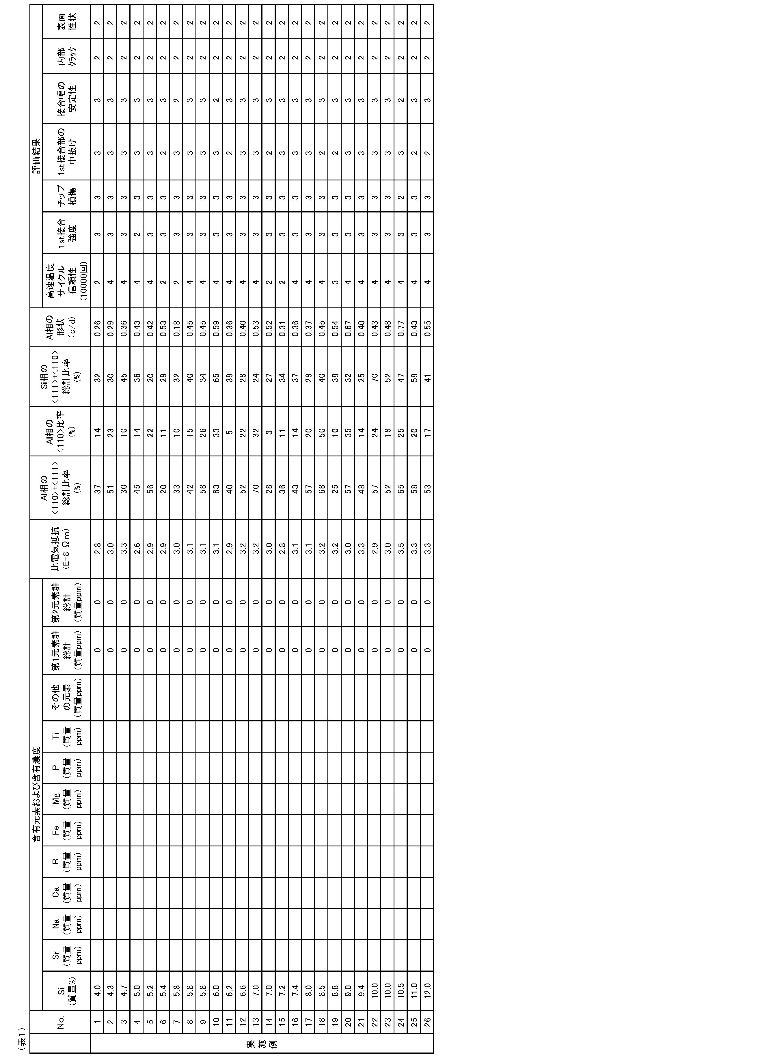
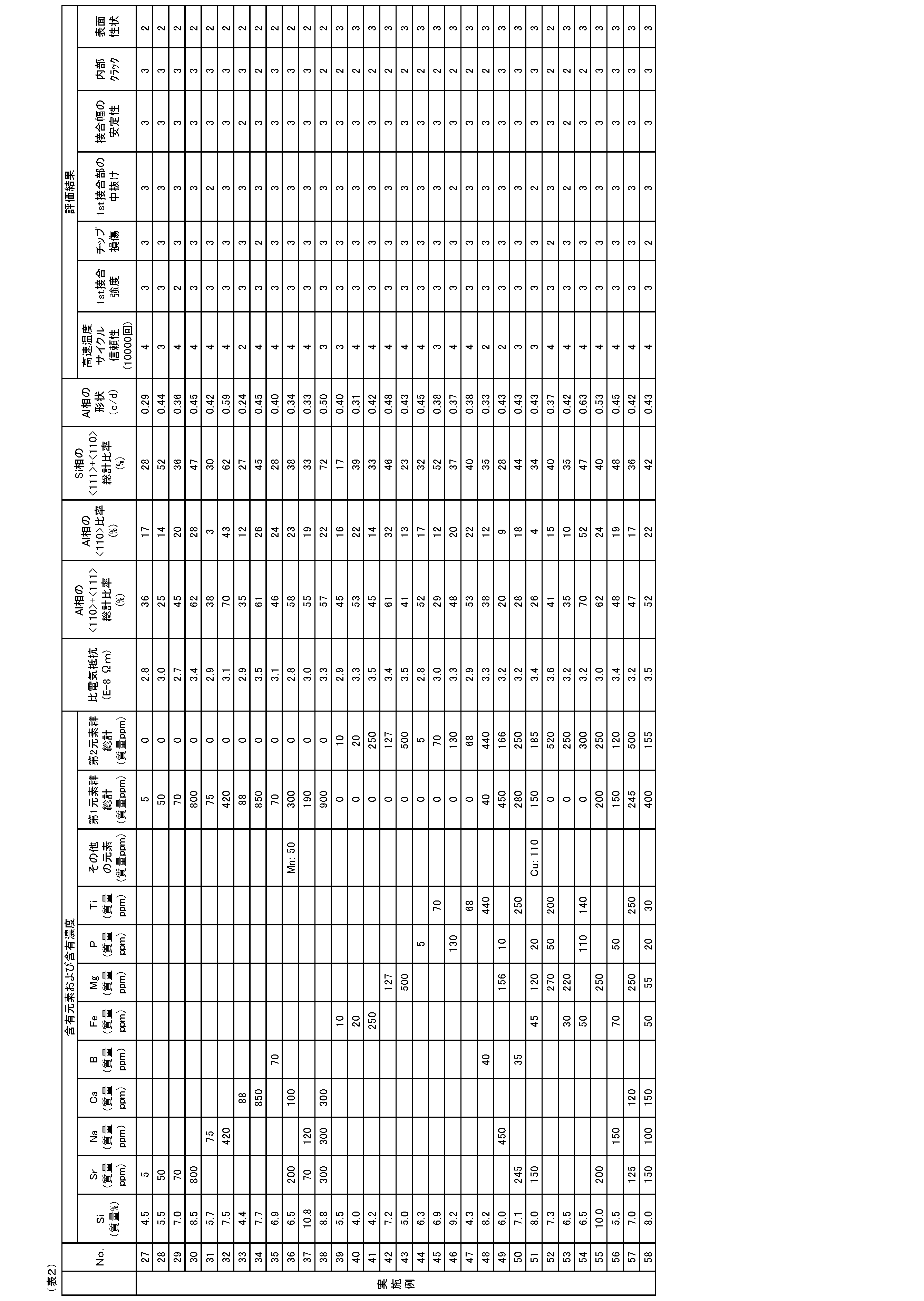
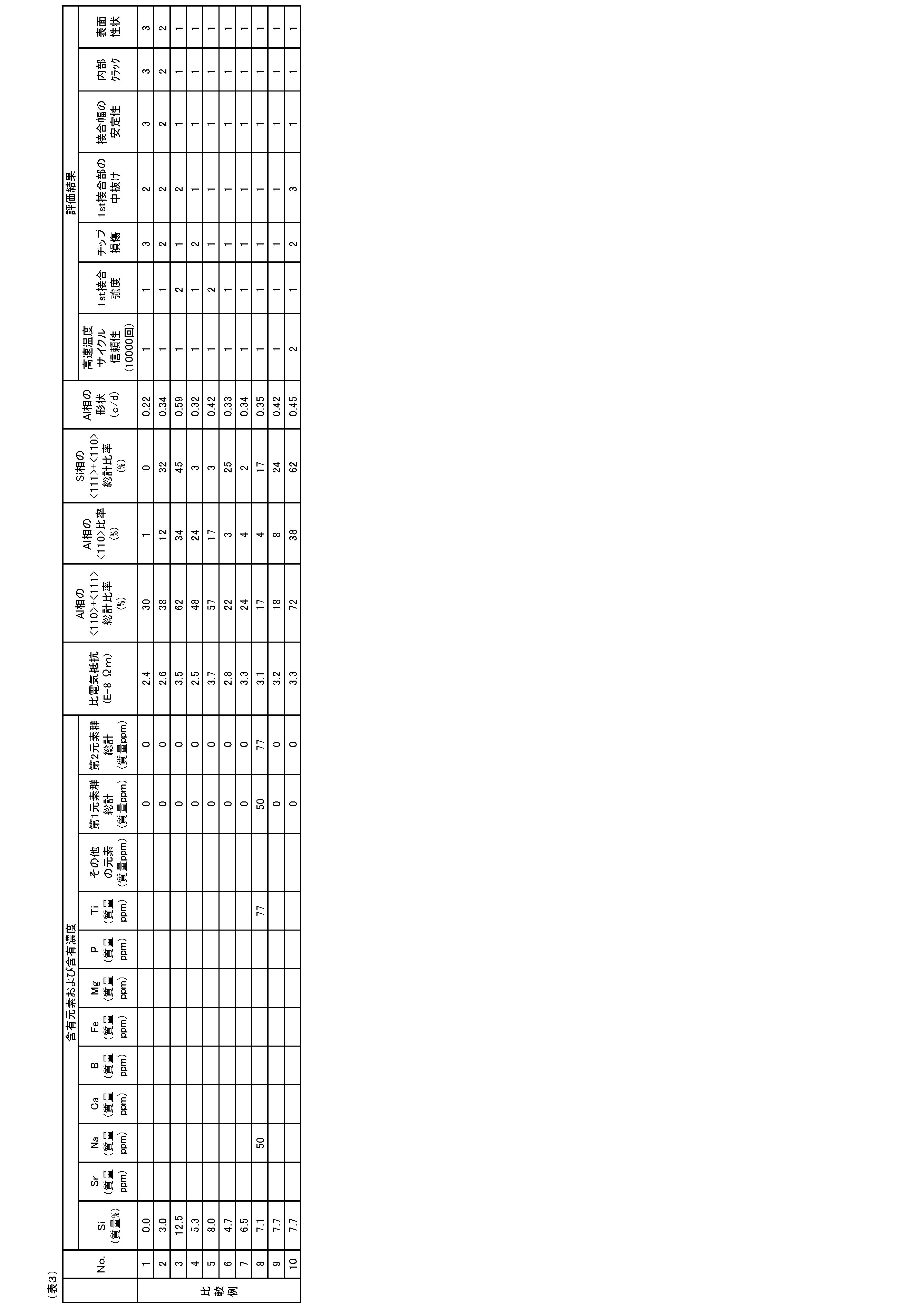
実施例No.1~58のAl接続材はいずれも、Siを4.0質量%以上12.0質量%以下含有すると共に、その比電気抵抗Raが2.6×10⁻⁸Ωm以上3.6×10⁻⁸Ωm以下であり、そのL断面におけるAl相の<110>+<111>総計比率が20%以上70%以下(但し該該方位比率の総計が25%以下のとき、中心軸方向に対して角度差が15°以下である<110>結晶方位の方位比率が5%以上)であり、高速TCTにおいても良好な温度サイクル信頼性を呈すると共に良好な1st接合強度を呈することを確認した。
加えて、L断面におけるAl相の<110>比率が5%以上50%以下である実施例No.1~13、15~30、32~50、52、53、55~58のAl接続材は、1st接合強度においてより良好な結果を呈し、また、1st接合部の中抜けを抑制し易いことを確認した。
L断面におけるSi相の<111>+<110>総計比率が20%以上70%以下である実施例No.1~37、40~58のAl接続材は、高速TCTにおいてよりいっそう良好な温度サイクル信頼性が得られる傾向にあることを確認した。
L断面におけるAl相の形状比率(c/d)の平均値が0.2以上0.7以下である実施例No.1~6、8~23、25~58のAl接続材は、接合時の接合幅のばらつきを低減させ、接合幅を安定化させ得る傾向にあることを確認した。
さらに、第1元素群(Sr、Na、Ca、B)の一種以上を総計で5質量ppm以上800質量ppm以下含有する実施例No.27~33、35~37、48~51、55~58のAl接続材は、加工時の内部クラックを低減させ得ることを確認した。
第2元素群(Fe、Mg、P、Ti)の一種以上を総計で5質量ppm以上500質量ppm以下含有する実施例No.39~51、53~58のAl接続材は、表面の傷、削れの発生を抑えて、平滑な表面を有することを確認した。
他方、比較例No.1~10のAl接続材は、Si濃度、比電気抵抗、L断面におけるAl相の<110>+<111>総計比率(該総計比率が25%以下の場合はAl相の<110>比率を含めて)のいずれかが本発明範囲外であり、高速温度サイクル信頼性および1st接合強度のいずれかが十分に得られないことを確認した。
加えて、L断面におけるAl相の<110>比率が5%以上50%以下である実施例No.1~13、15~30、32~50、52、53、55~58のAl接続材は、1st接合強度においてより良好な結果を呈し、また、1st接合部の中抜けを抑制し易いことを確認した。
L断面におけるSi相の<111>+<110>総計比率が20%以上70%以下である実施例No.1~37、40~58のAl接続材は、高速TCTにおいてよりいっそう良好な温度サイクル信頼性が得られる傾向にあることを確認した。
L断面におけるAl相の形状比率(c/d)の平均値が0.2以上0.7以下である実施例No.1~6、8~23、25~58のAl接続材は、接合時の接合幅のばらつきを低減させ、接合幅を安定化させ得る傾向にあることを確認した。
さらに、第1元素群(Sr、Na、Ca、B)の一種以上を総計で5質量ppm以上800質量ppm以下含有する実施例No.27~33、35~37、48~51、55~58のAl接続材は、加工時の内部クラックを低減させ得ることを確認した。
第2元素群(Fe、Mg、P、Ti)の一種以上を総計で5質量ppm以上500質量ppm以下含有する実施例No.39~51、53~58のAl接続材は、表面の傷、削れの発生を抑えて、平滑な表面を有することを確認した。
他方、比較例No.1~10のAl接続材は、Si濃度、比電気抵抗、L断面におけるAl相の<110>+<111>総計比率(該総計比率が25%以下の場合はAl相の<110>比率を含めて)のいずれかが本発明範囲外であり、高速温度サイクル信頼性および1st接合強度のいずれかが十分に得られないことを確認した。
Claims (7)
- Siを4.0質量%以上12.0質量%以下含有するAl接続材であって、
比電気抵抗Raが2.6×10⁻⁸Ωm以上3.6×10⁻⁸Ωm以下であり、
該Al接続材のL断面(中心軸を含む中心軸方向の断面)におけるAl相の結晶方位を測定したとき、中心軸に対して角度差が15°以下である<110>結晶方位と<111>結晶方位の方位比率の総計が20%以上70%以下であり、但し該方位比率の総計が25%以下のとき、中心軸方向に対して角度差が15°以下である<110>結晶方位の方位比率が5%以上である、Al接続材。 - L断面におけるAl相の結晶方位について、中心軸方向に対して角度差が15°以下である<110>結晶方位の方位比率が5%以上50%以下である、請求項1に記載のAl接続材。
- L断面におけるSi相の結晶方位を測定したとき、中心軸方向に対して角度差が15°以下である<111>結晶方位と<110>結晶方位の方位比率の総計が20%以上70%以下である、請求項1又は2に記載のAl接続材。
- L断面におけるAl相の短辺長さcと長辺長さdの比率(c/d)の平均値が0.2以上0.7以下である、請求項1~3のいずれか1項に記載のAl接続材。
- さらにSr、Na、Ca、Bのいずれか一種以上を総計で5質量ppm以上800質量ppm以下含有する、請求項1~4のいずれか1項に記載のAl接続材。
- さらにFe、Mg、P、Tiのいずれか一種以上を総計で5質量ppm以上500質量ppm以下含有する、請求項1~5のいずれか1項に記載のAl接続材。
- Al接続材中のその他の元素の総計濃度が0.5質量%以下である、請求項1~6のいずれか1項に記載のAl接続材。
Priority Applications (16)
| Application Number | Priority Date | Filing Date | Title |
|---|---|---|---|
| JP2024540705A JP7600475B1 (ja) | 2022-12-05 | 2024-06-04 | Al接続材 |
| JP2025537181A JP7733278B1 (ja) | 2023-11-27 | 2024-11-27 | Alボンディングワイヤ又はAlボンディングリボン |
| PCT/JP2024/042020 WO2025115915A1 (ja) | 2023-11-27 | 2024-11-27 | Alボンディングワイヤ又はAlボンディングリボン |
| JP2025537182A JP7733279B1 (ja) | 2023-11-27 | 2024-11-27 | Alボンディングワイヤ又はAlボンディングリボン |
| JP2025537179A JP7742006B1 (ja) | 2023-11-27 | 2024-11-27 | Alボンディングワイヤ又はAlボンディングリボン |
| TW113145851A TW202538068A (zh) | 2023-11-27 | 2024-11-27 | 鋁接合線或鋁接合帶 |
| PCT/JP2024/042021 WO2025115916A1 (ja) | 2023-11-27 | 2024-11-27 | Alボンディングワイヤ又はAlボンディングリボン |
| PCT/JP2024/042019 WO2025115914A1 (ja) | 2023-11-27 | 2024-11-27 | Alボンディングワイヤ又はAlボンディングリボン |
| PCT/JP2024/042018 WO2025115913A1 (ja) | 2023-11-27 | 2024-11-27 | Alボンディングワイヤ又はAlボンディングリボン |
| JP2025537178A JP7742005B1 (ja) | 2023-11-27 | 2024-11-27 | Alボンディングワイヤ又はAlボンディングリボン |
| TW113145850A TW202528553A (zh) | 2023-11-27 | 2024-11-27 | 鋁接合線或鋁接合帶 |
| TW113145854A TW202531556A (zh) | 2023-11-27 | 2024-11-27 | 鋁接合線或鋁接合帶 |
| PCT/JP2024/042022 WO2025115917A1 (ja) | 2023-11-27 | 2024-11-27 | Alボンディングワイヤ又はAlボンディングリボン |
| TW113145855A TW202528555A (zh) | 2023-11-27 | 2024-11-27 | 鋁接合線或鋁接合帶 |
| TW113145852A TW202528554A (zh) | 2023-11-27 | 2024-11-27 | 鋁接合線或鋁接合帶 |
| JP2025537180A JP7733858B1 (ja) | 2023-11-27 | 2024-11-27 | Alボンディングワイヤ又はAlボンディングリボン |
Applications Claiming Priority (11)
| Application Number | Priority Date | Filing Date | Title |
|---|---|---|---|
| JP2022194009 | 2022-12-05 | ||
| JPPCT/JP2023/042373 | 2023-11-27 | ||
| JPPCT/JP2023/042369 | 2023-11-27 | ||
| JPPCT/JP2023/042366 | 2023-11-27 | ||
| JPPCT/JP2023/042374 | 2023-11-27 | ||
| PCT/JP2023/042369 WO2024122381A1 (ja) | 2022-12-05 | 2023-11-27 | Al接続材 |
| PCT/JP2023/042371 WO2024122382A1 (ja) | 2022-12-05 | 2023-11-27 | Al接続材 |
| PCT/JP2023/042366 WO2024122380A1 (ja) | 2022-12-05 | 2023-11-27 | Al接続材 |
| PCT/JP2023/042374 WO2024122384A1 (ja) | 2022-12-05 | 2023-11-27 | Al接続材 |
| JPPCT/JP2023/042371 | 2023-11-27 | ||
| PCT/JP2023/042373 WO2024122383A1 (ja) | 2022-12-05 | 2023-11-27 | Al接続材 |
Publications (1)
| Publication Number | Publication Date |
|---|---|
| WO2025115258A1 true WO2025115258A1 (ja) | 2025-06-05 |
Family
ID=91379118
Family Applications (8)
| Application Number | Title | Priority Date | Filing Date |
|---|---|---|---|
| PCT/JP2023/024324 Ceased WO2024122089A1 (ja) | 2022-12-05 | 2023-06-30 | Al合金ボンディングワイヤ |
| PCT/JP2023/042366 Ceased WO2024122380A1 (ja) | 2022-12-05 | 2023-11-27 | Al接続材 |
| PCT/JP2023/042369 Ceased WO2024122381A1 (ja) | 2022-12-05 | 2023-11-27 | Al接続材 |
| PCT/JP2023/042373 Ceased WO2024122383A1 (ja) | 2022-12-05 | 2023-11-27 | Al接続材 |
| PCT/JP2023/042371 Ceased WO2024122382A1 (ja) | 2022-12-05 | 2023-11-27 | Al接続材 |
| PCT/JP2023/042374 Ceased WO2024122384A1 (ja) | 2022-12-05 | 2023-11-27 | Al接続材 |
| PCT/JP2024/020313 Pending WO2025115257A1 (ja) | 2022-12-05 | 2024-06-04 | Al接続材 |
| PCT/JP2024/020314 Pending WO2025115258A1 (ja) | 2022-12-05 | 2024-06-04 | Al接続材 |
Family Applications Before (7)
| Application Number | Title | Priority Date | Filing Date |
|---|---|---|---|
| PCT/JP2023/024324 Ceased WO2024122089A1 (ja) | 2022-12-05 | 2023-06-30 | Al合金ボンディングワイヤ |
| PCT/JP2023/042366 Ceased WO2024122380A1 (ja) | 2022-12-05 | 2023-11-27 | Al接続材 |
| PCT/JP2023/042369 Ceased WO2024122381A1 (ja) | 2022-12-05 | 2023-11-27 | Al接続材 |
| PCT/JP2023/042373 Ceased WO2024122383A1 (ja) | 2022-12-05 | 2023-11-27 | Al接続材 |
| PCT/JP2023/042371 Ceased WO2024122382A1 (ja) | 2022-12-05 | 2023-11-27 | Al接続材 |
| PCT/JP2023/042374 Ceased WO2024122384A1 (ja) | 2022-12-05 | 2023-11-27 | Al接続材 |
| PCT/JP2024/020313 Pending WO2025115257A1 (ja) | 2022-12-05 | 2024-06-04 | Al接続材 |
Country Status (8)
| Country | Link |
|---|---|
| US (1) | US20250379177A1 (ja) |
| EP (4) | EP4534709A4 (ja) |
| JP (6) | JP7518305B1 (ja) |
| KR (4) | KR20250114537A (ja) |
| CN (4) | CN118660981A (ja) |
| DE (1) | DE112023005086T5 (ja) |
| TW (4) | TW202432852A (ja) |
| WO (8) | WO2024122089A1 (ja) |
Families Citing this family (3)
| Publication number | Priority date | Publication date | Assignee | Title |
|---|---|---|---|---|
| JP7600474B1 (ja) * | 2022-12-05 | 2024-12-16 | 日鉄ケミカル&マテリアル株式会社 | Al接続材 |
| JP7600475B1 (ja) * | 2022-12-05 | 2024-12-16 | 日鉄ケミカル&マテリアル株式会社 | Al接続材 |
| DE112023005086T5 (de) * | 2022-12-05 | 2025-10-23 | Nippon Micrometal Corporation | Al-Legierungs-Bonddraht |
Citations (5)
| Publication number | Priority date | Publication date | Assignee | Title |
|---|---|---|---|---|
| WO2019031498A1 (ja) * | 2017-08-09 | 2019-02-14 | 日鉄ケミカル&マテリアル株式会社 | 半導体装置用Cu合金ボンディングワイヤ |
| WO2019031497A1 (ja) * | 2017-08-09 | 2019-02-14 | 日鉄ケミカル&マテリアル株式会社 | 半導体装置用Cu合金ボンディングワイヤ |
| WO2020184655A1 (ja) * | 2019-03-13 | 2020-09-17 | 日鉄マイクロメタル株式会社 | Alボンディングワイヤ |
| WO2022168787A1 (ja) * | 2021-02-05 | 2022-08-11 | 日鉄マイクロメタル株式会社 | 半導体装置用Alボンディングワイヤ |
| WO2024122384A1 (ja) * | 2022-12-05 | 2024-06-13 | 日鉄ケミカル&マテリアル株式会社 | Al接続材 |
Family Cites Families (15)
| Publication number | Priority date | Publication date | Assignee | Title |
|---|---|---|---|---|
| JPS5928553A (ja) * | 1982-08-11 | 1984-02-15 | Hitachi Ltd | 耐食性アルミニウム配線材料 |
| JPS5957440A (ja) | 1982-09-27 | 1984-04-03 | Tanaka Kikinzoku Kogyo Kk | 半導体素子用ボンデイング素線の製造方法 |
| JPS5967642A (ja) * | 1982-10-12 | 1984-04-17 | Hitachi Ltd | 半導体装置 |
| JPS59139661A (ja) * | 1983-01-31 | 1984-08-10 | Hitachi Ltd | 半導体装置 |
| JP2766933B2 (ja) * | 1989-06-29 | 1998-06-18 | 株式会社日立製作所 | 電子装置 |
| MY137479A (en) * | 2000-09-18 | 2009-01-30 | Nippon Steel Corp | Bonding wire for semiconductor device and method for producing the same |
| JP4633972B2 (ja) * | 2001-07-17 | 2011-02-16 | 住友電気工業株式会社 | 耐摩耗性アルミニウム合金長尺体およびその製造方法ならびにカーエアコンディショナ用ピストン |
| DE102004043020B3 (de) * | 2004-09-06 | 2006-04-27 | eupec Europäische Gesellschaft für Leistungshalbleiter mbH | Bonddraht und Bondverbindung |
| JP6272674B2 (ja) | 2012-11-30 | 2018-01-31 | 日本ピストンリング株式会社 | ボンディングワイヤ、接続部構造、並びに半導体装置およびその製造方法 |
| JP5281191B1 (ja) | 2012-12-28 | 2013-09-04 | 田中電子工業株式会社 | パワ−半導体装置用アルミニウム合金細線 |
| CN105331856B (zh) * | 2015-12-04 | 2018-05-22 | 江苏亨通电力特种导线有限公司 | 一种微合金化的Al-Si合金及其铝合金杆的制备方法 |
| JP2020150116A (ja) | 2019-03-13 | 2020-09-17 | ルネサスエレクトロニクス株式会社 | 半導体装置およびその製造方法 |
| CA3138936A1 (en) * | 2019-05-19 | 2020-11-26 | Novelis Inc. | Aluminum alloys for fluxless brazing applications, methods of making the same, and uses thereof |
| CN110205511A (zh) | 2019-06-28 | 2019-09-06 | 江西理工大学 | 一种高强Al-Si合金焊丝及其制备方法 |
| CN110656263A (zh) * | 2019-11-06 | 2020-01-07 | 中国科学院金属研究所 | 含微量La元素的高性能Al-Si系焊丝合金及其制备方法 |
-
2023
- 2023-06-30 DE DE112023005086.4T patent/DE112023005086T5/de active Pending
- 2023-06-30 KR KR1020257021796A patent/KR20250114537A/ko active Pending
- 2023-06-30 JP JP2023579485A patent/JP7518305B1/ja active Active
- 2023-06-30 EP EP23900220.7A patent/EP4534709A4/en active Pending
- 2023-06-30 WO PCT/JP2023/024324 patent/WO2024122089A1/ja not_active Ceased
- 2023-06-30 US US18/874,698 patent/US20250379177A1/en active Pending
- 2023-06-30 CN CN202380020896.7A patent/CN118660981A/zh active Pending
- 2023-11-27 WO PCT/JP2023/042366 patent/WO2024122380A1/ja not_active Ceased
- 2023-11-27 KR KR1020257021989A patent/KR20250116123A/ko active Pending
- 2023-11-27 EP EP23900500.2A patent/EP4632092A1/en active Pending
- 2023-11-27 WO PCT/JP2023/042369 patent/WO2024122381A1/ja not_active Ceased
- 2023-11-27 EP EP23900498.9A patent/EP4632090A1/en active Pending
- 2023-11-27 CN CN202380083564.3A patent/CN120303422A/zh active Pending
- 2023-11-27 EP EP23900499.7A patent/EP4632091A1/en active Pending
- 2023-11-27 JP JP2024536442A patent/JP7833550B2/ja active Active
- 2023-11-27 CN CN202380083554.XA patent/CN120435577A/zh active Pending
- 2023-11-27 KR KR1020257021779A patent/KR20250114535A/ko active Pending
- 2023-11-27 JP JP2024536441A patent/JP7626906B2/ja active Active
- 2023-11-27 JP JP2024536440A patent/JP7626905B2/ja active Active
- 2023-11-27 WO PCT/JP2023/042373 patent/WO2024122383A1/ja not_active Ceased
- 2023-11-27 KR KR1020257021793A patent/KR20250114536A/ko active Pending
- 2023-11-27 WO PCT/JP2023/042371 patent/WO2024122382A1/ja not_active Ceased
- 2023-11-27 WO PCT/JP2023/042374 patent/WO2024122384A1/ja not_active Ceased
- 2023-11-27 CN CN202380083569.6A patent/CN120303423A/zh active Pending
- 2023-12-01 TW TW112146769A patent/TW202432852A/zh unknown
- 2023-12-01 TW TW112146772A patent/TW202503076A/zh unknown
- 2023-12-01 TW TW112146768A patent/TW202430658A/zh unknown
- 2023-12-01 TW TW112146773A patent/TW202432853A/zh unknown
-
2024
- 2024-06-04 WO PCT/JP2024/020313 patent/WO2025115257A1/ja active Pending
- 2024-06-04 WO PCT/JP2024/020314 patent/WO2025115258A1/ja active Pending
- 2024-07-04 JP JP2024107900A patent/JP2024138348A/ja active Pending
-
2025
- 2025-04-16 JP JP2025067311A patent/JP2025108597A/ja active Pending
Patent Citations (5)
| Publication number | Priority date | Publication date | Assignee | Title |
|---|---|---|---|---|
| WO2019031498A1 (ja) * | 2017-08-09 | 2019-02-14 | 日鉄ケミカル&マテリアル株式会社 | 半導体装置用Cu合金ボンディングワイヤ |
| WO2019031497A1 (ja) * | 2017-08-09 | 2019-02-14 | 日鉄ケミカル&マテリアル株式会社 | 半導体装置用Cu合金ボンディングワイヤ |
| WO2020184655A1 (ja) * | 2019-03-13 | 2020-09-17 | 日鉄マイクロメタル株式会社 | Alボンディングワイヤ |
| WO2022168787A1 (ja) * | 2021-02-05 | 2022-08-11 | 日鉄マイクロメタル株式会社 | 半導体装置用Alボンディングワイヤ |
| WO2024122384A1 (ja) * | 2022-12-05 | 2024-06-13 | 日鉄ケミカル&マテリアル株式会社 | Al接続材 |
Also Published As
Similar Documents
| Publication | Publication Date | Title |
|---|---|---|
| JP7626905B2 (ja) | Al接続材 | |
| JP7784391B2 (ja) | 半導体装置用Alボンディングワイヤ | |
| JP7600475B1 (ja) | Al接続材 | |
| JP7600474B1 (ja) | Al接続材 | |
| JP7742005B1 (ja) | Alボンディングワイヤ又はAlボンディングリボン | |
| TWI922860B (zh) | Al連接材料 | |
| TWI922861B (zh) | Al連接材料 | |
| TW202548954A (zh) | Al連接材料 | |
| TW202548041A (zh) | Al連接材料 |
Legal Events
| Date | Code | Title | Description |
|---|---|---|---|
| ENP | Entry into the national phase |
Ref document number: 2024540705 Country of ref document: JP Kind code of ref document: A |
|
| WWE | Wipo information: entry into national phase |
Ref document number: 2024540705 Country of ref document: JP |
|
| 121 | Ep: the epo has been informed by wipo that ep was designated in this application |
Ref document number: 24896950 Country of ref document: EP Kind code of ref document: A1 |