WO2025115253A1 - 半導体装置、モジュール部材、及び回路基板 - Google Patents
半導体装置、モジュール部材、及び回路基板 Download PDFInfo
- Publication number
- WO2025115253A1 WO2025115253A1 PCT/JP2024/019382 JP2024019382W WO2025115253A1 WO 2025115253 A1 WO2025115253 A1 WO 2025115253A1 JP 2024019382 W JP2024019382 W JP 2024019382W WO 2025115253 A1 WO2025115253 A1 WO 2025115253A1
- Authority
- WO
- WIPO (PCT)
- Prior art keywords
- semiconductor device
- main surface
- thickness direction
- layer
- hole
- Prior art date
- Legal status (The legal status is an assumption and is not a legal conclusion. Google has not performed a legal analysis and makes no representation as to the accuracy of the status listed.)
- Pending
Links
Images








Classifications
-
- H—ELECTRICITY
- H01—ELECTRIC ELEMENTS
- H01G—CAPACITORS; CAPACITORS, RECTIFIERS, DETECTORS, SWITCHING DEVICES, LIGHT-SENSITIVE OR TEMPERATURE-SENSITIVE DEVICES OF THE ELECTROLYTIC TYPE
- H01G4/00—Fixed capacitors; Processes of their manufacture
- H01G4/30—Stacked capacitors
-
- H—ELECTRICITY
- H01—ELECTRIC ELEMENTS
- H01G—CAPACITORS; CAPACITORS, RECTIFIERS, DETECTORS, SWITCHING DEVICES, LIGHT-SENSITIVE OR TEMPERATURE-SENSITIVE DEVICES OF THE ELECTROLYTIC TYPE
- H01G4/00—Fixed capacitors; Processes of their manufacture
- H01G4/33—Thin- or thick-film capacitors (thin- or thick-film circuits; capacitors without a potential-jump or surface barrier specially adapted for integrated circuits, details thereof, multistep manufacturing processes therefor)
-
- H—ELECTRICITY
- H10—SEMICONDUCTOR DEVICES; ELECTRIC SOLID-STATE DEVICES NOT OTHERWISE PROVIDED FOR
- H10W—GENERIC PACKAGES, INTERCONNECTIONS, CONNECTORS OR OTHER CONSTRUCTIONAL DETAILS OF DEVICES COVERED BY CLASS H10
- H10W70/00—Package substrates; Interposers; Redistribution layers [RDL]
- H10W70/60—Insulating or insulated package substrates; Interposers; Redistribution layers
-
- H—ELECTRICITY
- H10—SEMICONDUCTOR DEVICES; ELECTRIC SOLID-STATE DEVICES NOT OTHERWISE PROVIDED FOR
- H10W—GENERIC PACKAGES, INTERCONNECTIONS, CONNECTORS OR OTHER CONSTRUCTIONAL DETAILS OF DEVICES COVERED BY CLASS H10
- H10W90/00—Package configurations
Definitions
- This disclosure relates to a semiconductor device having a capacitance section provided inside a trench section.
- Patent Document 1 discloses a capacitor that includes a substrate having a recess on its surface, and a dielectric film and a conductive film provided inside the recess.
- the object of this disclosure is therefore to provide a semiconductor device, module component, and circuit board that can reduce the effect of noise on the capacitance section in order to solve the above problems.
- the semiconductor device comprises: A semiconductor substrate having one main surface and another main surface that is spaced apart from the one main surface in a thickness direction and faces the opposite direction from the one main surface in the thickness direction, wherein at least one trench portion is provided in the one main surface, and a hole portion is provided that extends along the thickness direction, opens in at least one of the one main surface and the other main surface, and has an area larger than one of the trench portions as viewed along the thickness direction; a capacitance section provided at least inside the trench section and having a dielectric layer and two electrode layers sandwiching the dielectric layer; A filling portion is provided inside the hole and contains a conductive material.
- the module member comprises: The semiconductor device; Electronic components, The semiconductor device is provided on a mounting substrate having a front mounting surface on which the electronic components are mounted and a rear mounting surface that is a rear surface of the front mounting surface.
- the circuit board according to the present disclosure comprises: The modular member; a main board having the module member mounted on a surface thereof; The semiconductor device is located between the mounting board and the main board.
- This disclosure provides a semiconductor device, module component, and circuit board that can reduce the effect of noise on the capacitance section.
- FIG. 1 is a plan view of a semiconductor device according to an embodiment of the present disclosure.
- FIG. 2 is a schematic cross-sectional view showing a cross section taken along line II-II of FIG.
- FIG. 1 is an equivalent circuit diagram of a semiconductor device according to an embodiment of the present disclosure.
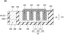
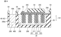
- Schematic cross-sectional views illustrating a method for manufacturing a semiconductor device according to an embodiment of the present disclosure Schematic cross-sectional views illustrating a method for manufacturing a semiconductor device according to an embodiment of the present disclosure. Schematic cross-sectional views illustrating a method for manufacturing a semiconductor device according to an embodiment of the present disclosure. Schematic cross-sectional views illustrating a method for manufacturing a semiconductor device according to an embodiment of the present disclosure. Schematic cross-sectional view of a modified example of a semiconductor device according to an embodiment of the present disclosure. Schematic cross-sectional view of a modified example of a semiconductor device according to an embodiment of the present disclosure. Schematic cross-sectional view of a modified example of a semiconductor device according to an embodiment of the present disclosure. Schematic cross-sectional view of a modified example of a semiconductor device according to an embodiment of the present disclosure.
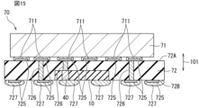
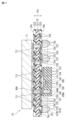
- Schematic cross-sectional view of a module member according to an embodiment of the present disclosure Schematic cross-sectional view of a modified example of a module member according to an embodiment of the present disclosure. Schematic cross-sectional view of a modified example of a module member according to an embodiment of the present disclosure. Schematic cross-sectional view of a circuit board according to an embodiment of the present disclosure.
- Fig. 1 is a plan view of a semiconductor device according to an embodiment of the present disclosure
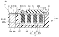
- Fig. 2 is a schematic cross-sectional view showing a cross section taken along line II-II of Fig. 1.
- the semiconductor device 10 includes a semiconductor substrate 20, a capacitance section 30, a filling section 40, a first insulating layer 53, a second insulating layer 54, and an external terminal 51.
- the semiconductor substrate 20 is, for example, a silicon (Si) substrate, and is made of insulating, high-resistance Si.
- the semiconductor substrate 20 has one principal surface 20A and the other principal surface 20B.
- the one principal surface 20A and the other principal surface 20B are spaced apart from each other in the thickness direction 101 of the semiconductor substrate 20.
- the one principal surface 20A and the other principal surface 20B face in opposite directions from each other in the thickness direction 101.
- the semiconductor substrate 20 has a recess 20E and four trench portions 20C.
- the recess 20E is filled with a first electrode layer 321 of the capacitance section 30, which will be described later.
- the first electrode layer 321 constitutes part of one main surface 20A of the semiconductor substrate 20.
- the first electrode layer 321 is part of the capacitance section 30 and also part of the semiconductor substrate 20.
- one recess 20E is shown, but the semiconductor substrate 20 is not limited to having one recess 20E.
- the semiconductor substrate 20 may have multiple recesses 20E.
- the four trench portions 20C are provided in a portion of the first electrode layer 321 that constitutes part of one main surface 20A, and are recessed in the thickness direction 101. In other words, each of the four trench portions 20C is a recess provided in one main surface 20A.
- the trench portion 20C may have any shape.
- the trench portion 20C may be circular or rectangular when viewed along the thickness direction 101, or may be a narrow groove that is curved or straight. This groove may branch into multiple parts.
- Each of the four trench portions 20C may have the same shape or different shapes.
- trench portions 20C are shown, but the number of trench portions 20C that the semiconductor substrate 20 has is not limited to four.
- the semiconductor substrate 20 only needs to have at least one trench portion 20C.
- the recess 20E and the trench portion 20C are provided on one main surface 20A, but the recess 20E and the trench portion 20C may be provided on the other main surface 20B, or may be provided on both the one main surface 20A and the other main surface 20B.
- the semiconductor substrate 20 has a hole 20D.
- the hole 20D penetrates the semiconductor substrate 20 in the thickness direction 101. That is, the hole 20D extends in the thickness direction 101 and opens to one main surface 20A and the other main surface 20B.
- the hole 20D has a side surface 20Da.
- the hole 20D is circular when viewed along the thickness direction 101. That is, the hole 20D is cylindrical.
- the hole 20D does not have to penetrate the semiconductor substrate 20 in the thickness direction 101.
- the hole 20D may be open to only one of the first main surface 20A and the second main surface 20B.
- the hole 20D may be a recess provided in the first main surface 20A, as in the modified example of FIG. 13 described below.
- the hole 20D may be a recess provided in the second main surface 20B.
- the shape of the hole 20D is arbitrary, just like the shape of the trench 20C.
- the hole 20D may be circular or rectangular when viewed along the thickness direction 101, or may be a narrow groove that is curved or straight. This groove may be branched into multiple parts.
- the hole portion 20D When viewed along the thickness direction 101, the hole portion 20D has a larger area than each of the four trench portions 20C. In other words, when viewed along the thickness direction 101, the hole portion 20D has a larger area than one trench portion 20C.
- the width of hole portion 20D is greater than the width of each of the four trench portions 20C.
- the width of hole portion 20D is defined, for example, as follows. When hole portion 20D is circular when viewed along thickness direction 101, the width of hole portion 20D is the diameter of the circle. When hole portion 20D is rectangular when viewed along thickness direction 101, the width of hole portion 20D is the length of the short side of the rectangle. When hole portion 20D is a narrow groove when viewed along thickness direction 101, the width of hole portion 20D is in a direction perpendicular to the direction in which the groove extends. The above definitions also apply to the width of trench portion 20C.
- the width of the hole 20D is at least twice the width of each of the four trench portions 20C (see FIG. 2).
- the width of the hole 20D is at least five times the width of each of the four trench portions 20C. More preferably, the width of the hole 20D is at least ten times the width of each of the four trench portions 20C (see FIG. 11).
- one hole 20D is shown, but the semiconductor substrate 20 is not limited to having one hole 20D.
- the semiconductor substrate 20 may have multiple holes 20D.
- the capacitance section 30 is provided inside the recess 20E, inside the trench section 20C, and on one of the main surfaces 20A. In other words, the capacitance section 30 is provided at least inside the trench section 20C.
- the capacitance section 30 has a dielectric layer and an electrode layer.
- the capacitance section 30 has two dielectric layers (a first dielectric layer 311 and a second dielectric layer 312) and three electrode layers (a first electrode layer 321, a second electrode layer 322, and a third electrode layer 323).
- the dielectric layer includes a dielectric.
- the dielectric layer is made of a dielectric material such as silicon dioxide (SiO 2 ), silicon nitride (Si 3 N 4 ), hafnium oxide (HfO 2 ), aluminum oxide (AlO), etc.
- the first dielectric layer 311 and the second dielectric layer 312 may be made of the same material or different materials.
- the electrode layer includes a conductor.
- the electrode layer is made of a conductor such as a metal such as copper, low-resistance silicon (Si) such as conductive n-type Si or p-type Si, or polysilicon (Poly-Si).
- the first electrode layer 321, the second electrode layer 322, and the third electrode layer 323 may be made of the same material or different materials.
- the first electrode layer 321 is provided inside the recess 20E.
- the first electrode layer 321 is made of low-resistance silicon (Si).
- the first electrode layer 321 may be electrically connected to the other main surface 20B.
- the first electrode layer 321 has four trench portions 20C in a portion that constitutes part of the one main surface 20A.
- the first dielectric layer 311 is laminated on the first electrode layer 321 and the semiconductor substrate 20 across the inside and outside of the four trench portions 20C.
- the first dielectric layer 311 is laminated on the first electrode layer 321 along the trench portions 20C inside the four trench portions 20C.
- the first dielectric layer 311 is laminated on the first electrode layer 321 and one main surface 20A of the semiconductor substrate 20 outside the four trench portions 20C.
- the second dielectric layer 312 is laminated on the second electrode layer 322 inside and outside the four trench portions 20C.
- the second dielectric layer 312 is laminated on the second electrode layer 322 inside the four trench portions 20C and along the trench portions 20C.
- the third electrode layer 323 is laminated on the second dielectric layer 312 across the inside and outside of the four trench portions 20C.
- the third electrode layer 323 is laminated on the second dielectric layer 312 so as to fill the spaces not shown in the first dielectric layer 311, the second electrode layer 322, and the second dielectric layer 312 inside the four trench portions 20C.
- the capacitance section 30 has at least a dielectric layer and two electrode layers sandwiching the dielectric layer.
- the capacitance section 30 has two sets of a dielectric layer and two electrode layers sandwiching the dielectric layer.
- One of the two sets is composed of the first dielectric layer 311, and the first electrode layer 321 and the second electrode layer 322 that sandwich the first dielectric layer 311.
- the other of the two sets is composed of the second dielectric layer 312, and the second electrode layer 322 and the third electrode layer 323 that sandwich the second dielectric layer 312.
- the capacitance section 30 may have only one set of a dielectric layer and two electrode layers sandwiching the dielectric layer, or may have three or more sets.
- the filling portion 40 is provided inside the hole 20D.
- the filling portion 40 extends from one end to the other end in the thickness direction 101 of the hole 20D.
- the upper surface 40A of the filling portion 40 is a portion of the filling portion 40 located at one end of the hole 20D in the thickness direction 101.
- the upper surface 40A of the filling portion 40 constitutes a part of one main surface 20A of the semiconductor substrate 20.
- the lower surface 40B of the filling portion 40 is a portion of the filling portion 40 located at the other end of the hole 20D in the thickness direction 101.
- the lower surface 40B of the filling portion 40 constitutes a part of the other main surface 20B of the semiconductor substrate 20.
- the filling portion 40 contains a conductive material.
- the filling portion 40 is composed of a conductive layer 42 made of copper as the conductive material.
- the filling portion 40 is composed only of a conductive material, but the filling portion 40 may contain a material other than the conductive material. An example in which the filling portion 40 contains a material other than the conductive material will be described later.
- the first insulating layer 53 and the second insulating layer 54 are made of an insulator.
- the first insulating layer 53 and the second insulating layer 54 may be made of an inorganic or organic material as long as the material has high insulating properties.
- the first insulating layer 53 is laminated so as to cover a part of the part of the first electrode layer 321, the second electrode layer 322, the third electrode layer 323, the first dielectric layer 311, and the second dielectric layer 312 that is exposed on the one main surface 20A side of the semiconductor substrate 20.
- the second insulating layer 54 is laminated so as to cover a part of the one main surface 20A of the semiconductor substrate 20 and a part of the part of the second dielectric layer 312, the second electrode layer 322, and the third electrode layer 323 that is exposed on the one main surface 20A side of the semiconductor substrate 20.
- the external terminal 51 is provided on at least one of the first main surface 20A and the second main surface 20B.
- the external terminal 51 is made of a conductive material such as nickel (Ni) or gold (Au).
- the external terminal 51 is a multi-layer structure of copper (Cu), nickel, and gold.
- the external terminal 51 includes a first external terminal 511, a second external terminal 512, and a third external terminal 513.
- the first external terminal 511, the second external terminal 512, and the third external terminal 513 are all provided on the first main surface 20A side of the semiconductor substrate 20.
- the first external terminal 511, the second external terminal 512, and the third external terminal 513 are insulated from each other by the second insulating layer 54.
- the first external terminal 511, the second external terminal 512, and the third external terminal 513 are made of the same material, but may be made of different materials.
- the first external terminal 511 is laminated on the first electrode layer 321, the third electrode layer 323, and the first insulating layer 53. As a result, the first external terminal 511 is in contact with the first electrode layer 321 and the third electrode layer 323. In other words, the first electrode layer 321 and the third electrode layer 323 are electrically connected to each other via the first external terminal 511.
- a first insulating layer 53 is provided between the first external terminal 511 and the first dielectric layer 311, the second electrode layer 322, and the second dielectric layer 312.
- the first external terminal 511 is insulated from the first dielectric layer 311, the second electrode layer 322, and the second dielectric layer 312 by the first insulating layer 53.
- the second external terminal 512 is laminated on the second electrode layer 322. As a result, the second external terminal 512 and the second electrode layer 322 are in contact with each other and electrically connected.
- the third external terminal 513 is layered on the upper surface 40A of the filling section 40. As a result, the third external terminal 513 and the filling section 40 are in contact with each other and electrically connected.
- the third external terminal 513 is an example of an external terminal.
- FIG. 3 is an equivalent circuit diagram of a semiconductor device according to an embodiment of the present disclosure.
- the semiconductor device 10 is configured as described above, and thus constitutes a circuit as shown in FIG. 3.
- the equivalent circuit of the semiconductor device 10 is not limited to the circuit as shown in FIG. 3.
- a resistor R and capacitors C1 and C2 may be connected.
- the capacitor C1 is formed by the first dielectric layer 311 and the first electrode layer 321 and second electrode layer 322 which sandwich the first dielectric layer 311.
- the capacitor C2 is formed by the second dielectric layer 312 and the second electrode layer 322 and third electrode layer 323 which sandwich the second dielectric layer 312.
- One electrode of the capacitor C1 (first electrode layer 321) and one electrode of the capacitor C2 (third electrode layer 323) are connected to the first external terminal 511.
- the other electrodes of the capacitors C1 and C2 (second electrode layer 322) are connected to the second external terminal 512.
- the filling section 40 constitutes a resistor R.
- One end of the resistor R (upper surface 40A of the filling section 40) is connected to a third external terminal 513.
- the other end of the resistor R (lower surface 40B of the filling section 40) is not connected to an external terminal, but may be connected to an external terminal.
- An example in which the lower surface 40B of the filling section 40 is connected to an external terminal will be described later.
- the semiconductor device 10 described above has the following dimensions, for example. More specifically, the length in the thickness direction 101 is 0.15 mm, the length in the width direction 103 is 0.6 mm, and the length in the depth direction perpendicular to the thickness direction 101 and the width direction 103 is 0.3 mm.
- the depth (length in the thickness direction 101) of each of the first trench portion 20Ca and the second trench portion 20Cb is 30 ⁇ m.
- the thickness of the electrode layers (first electrode layer 321, second electrode layer 322, and third electrode layer 323) is 1000 nm. When the electrode layers are made of titanium nitride (TiN), the thickness of the electrode layers is 20 nm.
- the thickness of the dielectric layers (first dielectric layer 311 and second dielectric layer 312) is 10 nm.
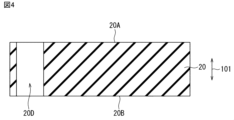
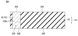
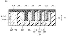
- FIG. 4 to 10 are schematic cross-sectional views for explaining the method for manufacturing the semiconductor device according to the embodiment of the present disclosure.
- the semiconductor device 10 is manufactured by singulating the laminate into multiple pieces.
- the laminate is an integrated structure in which multiple semiconductor devices 10 are arranged. For ease of explanation, only a portion of the laminate that corresponds to one semiconductor device 10 is shown in Figures 4 to 10.
- the manufacturing method for the semiconductor device 10 according to this embodiment includes a hole forming process, a filling portion forming process, a capacitance portion forming process (an electrode layer forming process, a dielectric layer forming process, and a trench portion forming process), a first insulating layer forming process, a second insulating layer forming process, an external terminal forming process, and a singulation process.
- a hole forming step is performed.
- a hole 20D penetrating the semiconductor substrate 20 in the thickness direction 101 is formed in the semiconductor substrate 20.
- a hard mask is formed on the semiconductor substrate 20, a pattern corresponding to the hole 20D is performed on the hard mask, and deep silicon etching is performed to form the hole 20D in the semiconductor substrate 20. After the deep silicon etching is performed, the hard mask is removed.
- a filling portion forming process is performed.
- a conductive paste is filled into the hole 20D.
- This paste corresponds to the conductive layer 42 of the filling portion 40.
- a seed is formed, via-filling plating is performed, and the seed is removed and flattened to form the filling portion 40.
- the filling portion 40 may be filled by a method other than the above-mentioned formation method.
- a conductive material such as copper (Cu) or aluminum (Al) as the filling portion 40 may be filled by a method such as sputtering, wet plating, and paste.
- a capacitive portion forming step is carried out, which is divided into an electrode layer forming step, a dielectric layer forming step, and a trench portion forming step.
- the electrode layer forming process and the dielectric layer forming process are performed alternately.
- the trench portion forming process is performed after the first electrode layer forming process and before the first dielectric layer forming process.
- impurity doping is performed on the semiconductor substrate 20 as a high resistance portion formed of high resistance Si.
- a recess 20E is formed in the semiconductor substrate 20 as a high resistance portion, and a first electrode layer 321 is formed as a low resistance portion in the recess 20E.
- the first electrode layer 321 is formed, for example, by forming a patterned resist at the position of the recess 20E, performing silicon etching doped with impurities, and removing the resist.
- trench portions 20C are formed in a portion of one main surface 20A of the first electrode layer 321.
- the trench portions 20C are formed, for example, by patterning a hard mask and deep silicon etching, similar to the hole portions 20D.
- a dielectric layer forming process and an electrode layer forming process are alternately performed.
- the dielectric layer and the electrode layer are alternately stacked (deposited) on one main surface 20A of the semiconductor substrate 20 and on the surface constituting the trench portion 20C.
- a first dielectric layer 311 is formed on the semiconductor substrate 20, the filling portion 40, and the first electrode layer 321.
- a second electrode layer 322 is formed on the first dielectric layer 311.
- a second dielectric layer 312 is formed on the second electrode layer 322.
- a third electrode layer 323 is formed on the second dielectric layer 312.
- the dielectric layer forming process and electrode layer forming process after the dielectric layers 311, 312 and electrode layers 322, 323 are formed, photolithography and etching are performed on the dielectric layers 311, 312 and electrode layers 322, 323. As a result, a portion of each of the dielectric layers 311, 312 and electrode layers 322, 323 is removed, as shown in FIG. 8.
- the trench portion forming process is defined as part of the capacitance portion forming process.
- the trench portion forming process may be defined separately from the capacitance portion forming process.
- the capacitance portion forming process is divided into an electrode layer forming process and a dielectric layer forming process. Then, after the electrode layer forming process of the first capacitance portion forming process is performed, the trench portion forming process is performed, and then the remaining steps of the capacitance portion forming process are performed.
- a first insulating layer forming process is performed.
- a first insulating layer 53 is laminated as shown in Fig. 9.
- the first insulating layer 53 is deposited on the upper surface (the surface on the one main surface 20A side) of Fig. 8, and is patterned by photolithography and dry etching into a position corresponding to the first insulating layer 53 in Fig. 9.
- a second insulating layer forming step is performed.
- a second insulating layer 54 is laminated.
- the second insulating layer 54 is deposited on the upper surface (surface on the one main surface 20A side) of Fig. 9, and is patterned by photolithography and dry etching at a position corresponding to the second insulating layer 54 in Fig. 10.
- the second insulating layer forming step may be performed before the first insulating layer forming step or may be performed in parallel with the first insulating layer forming step.
- the first insulating layer 53 and the second insulating layer 54 may be formed by known means other than deposition such as CVD (Chemical Vapor Deposition), for example, spin coating or film lamination.
- a protective layer which is an insulating layer, may be provided on the second insulating layer 54.
- the protective layer is an organic resin such as epoxy, polyimide, or acrylic.
- an external terminal forming process is performed.
- external terminals 51 first external terminal 511, second external terminal 512, and third external terminal 513.
- a conductive layer as the external terminal 51 is formed at a predetermined position (position shown in FIG. 2) on the upper surface (surface on the one main surface 20A side) of FIG. 10 by a known means such as metal sputtering, electroless plating, or paste.
- the external terminal 51 may be composed of a plurality of conductive layers. By forming the external terminal 51 with a plurality of conductive layers, the external terminal 51 has electromigration resistance and the barrier property and solder wettability of the external terminal 51 are improved.
- a singulation process is performed.
- the thickness of the semiconductor device 10 is adjusted, and the stack in which the plurality of semiconductor devices 10 are arranged is cut into the plurality of semiconductor devices 10.
- the filling portion 40 containing a conductive material can function as a shield against noise. This allows the filling portion 40 to reduce noise traveling from the outside of the capacitance portion 30 through the filling portion 40 toward the capacitance portion 30.
- the filled portion 40 as wiring in the semiconductor device 10
- the amount of wiring routed around the semiconductor device 10 can be reduced. This reduces the parasitic capacitance that occurs in the semiconductor device 10.
- the capacitor disclosed in Patent Document 1 has a dielectric film and a conductive film on the front side of the substrate, so it is not necessarily easy to handle signals from the back side of the substrate.
- the hole 20D can open to both the one main surface 20A and the other main surface 20B, in other words, the hole 20D can penetrate the semiconductor substrate 20 in the thickness direction 101. In this case, even if the capacitance portion 30 is provided on the one main surface 20A side of the semiconductor substrate 20, it is possible to easily handle signals from the other main surface 20B.
- the area of the hole 20D is larger than the area of one trench portion 20C when viewed along the thickness direction 101. This reduces the manufacturing variation of the hole 20D. As a result, it is easy to fill the hole 20D with the filling portion 40.
- FIG. 11 is a schematic cross-sectional view of a modified example of the semiconductor device according to the embodiment of the present disclosure.
- the semiconductor device 10 may have an external terminal 51 on the other main surface 20B.
- the semiconductor device 10 shown in FIG. 11 has a fourth external terminal 514 as the external terminal 51 on the other main surface 20B.
- the semiconductor device 10 may also have a dummy terminal 52 on at least one of the one main surface 20A and the other main surface 20B.
- the semiconductor device 10 shown in FIG. 11 has a dummy terminal 52 on the other main surface 20B.
- the fourth external terminal 514 and the dummy terminal 52 are made of a conductive material such as nickel (Ni) or gold (Au).
- the fourth external terminal 514 is laminated on the lower surface 40B of the filling section 40. This allows the fourth external terminal 514 and the filling section 40 to come into contact with each other and be electrically connected.
- the dummy terminal 52 is laminated on the other main surface 20B of the semiconductor substrate 20.
- the dummy terminal 52 is not electrically connected to other conductive parts of the semiconductor device 10.
- the other conductive parts are, for example, the first electrode layer 321, the second electrode layer 322, the third electrode layer 323, the filling portion 40, and the external terminal 51.
- the mounting when mounting the semiconductor device 10 on a substrate via a paste such as solder, the mounting can be easily performed by attaching the paste to the external terminals 51.
- the mounting when mounting the semiconductor device 10 on a substrate via a paste such as solder, the mounting can be performed by attaching the paste to the dummy terminals 52.
- a paste such as solder
- the first modification when mounting, more paste can be attached than in a semiconductor device that does not have the dummy terminals 52. As a result, the strength of the mounting can be increased.
- FIG. 12 is a schematic cross-sectional view of a modified example of the semiconductor device according to the embodiment of the present disclosure.
- the filling portion 40 may contain a material other than a conductive material.
- the filling portion 40 shown in FIG. 12 includes an embedded layer 41, a barrier layer 43, and an isolation layer 44.
- the embedding layer 41 is made of a resin such as epoxy.
- the barrier layer 43 contains a conductive material such as titanium nitride (TiN) or nickel (Ni).
- the isolation layer 44 is made of an insulating material such as silicon dioxide (SiO 2 ) or silicon nitride (Si 3 N 4 ).
- the filling portion 40 of the semiconductor device 10 shown in FIG. 12 contains a conductive material in the conductive layer 42 and barrier layer 43, which are parts of the filling portion 40, and does not contain a conductive material in the embedding layer 41 and isolation layer 44, which are other parts.
- each of the embedded layer 41, the conductive layer 42, the barrier layer 43, and the isolation layer 44 penetrates the hole 20D in the thickness direction 101.
- each of the embedded layer 41, the conductive layer 42, the barrier layer 43, and the isolation layer 44 extends from one end of the hole 20D in the thickness direction 101 to the other end.
- the conductive layer 42 surrounds the embedded layer 41.
- the barrier layer 43 surrounds the conductive layer 42.
- the isolation layer 44 surrounds the barrier layer 43. The outer peripheral surface of the isolation layer 44 is in contact with the side surface 20Da of the hole portion 20D.
- the filling section 40 may not include at least one of the embedded layer 41 and the barrier layer 43.
- a magnetic layer 45 (described later) may be provided between two adjacent layers among the embedded layer 41, the conductive layer 42, the barrier layer 43, and the isolation layer 44.
- the isolation layer 44 is made of an insulating material. Therefore, the isolation layer 44 can block the unintended propagation of electrical signals from the conductive layer 42 through the semiconductor substrate 20 to other parts such as the capacitance section 30.
- the barrier layer 43 can suppress the diffusion of the conductive layer 42. Therefore, the change in the electrical resistance of the conductive layer 42 can be reduced.
- the barrier layer 43 since the barrier layer 43 contains a conductive material, the barrier layer 43 can function as a seed layer. In addition, an electrical signal can be passed through the barrier layer 43.
- the filling portion 40 has an embedded layer 41, which can suppress unnecessary voids, foreign matter contamination, and unevenness in the exposed portions of the filling portion 40 on the one main surface 20A and the other main surface 20B.
- the filling portion 40 has an embedded layer 41, which can eliminate the need to fill the entire hole 20D with the conductive layer 42. This can reduce the manufacturing cost of the semiconductor device 10.
- FIG. 13 is a schematic cross-sectional view of a modified example of the semiconductor device according to the embodiment of the present disclosure.
- the hole 20D may open to one of the first main surface 20A and the other main surface 20B and have a bottom on the other of the first main surface 20A and the other main surface 20B.
- the hole 20D opens to the first main surface 20A and has a bottom on the other main surface 20B side.
- the hole 20D has a side surface 20Da and a bottom surface 20Db.
- the side surface 20Da extends from one of the first main surface 20A and the other main surface 20B to the other.
- the side surface 20Da extends from the first main surface 20A to the other main surface 20B.
- the bottom surface 20Db is connected to the end of the side surface 20Da on the other side of the first main surface 20A and the other main surface 20B.
- the bottom surface 20Db is connected to the end of the side surface 20Da on the other main surface 20B side.
- the boundary 20Dc between the side surface 20Da and the bottom surface 20Db is a curved surface. In other words, the boundary 20Dc between the side surface 20Da and the bottom surface 20Db does not have a corner.
- the hole 20D may open to the other main surface 20B and have a bottom on the one main surface 20A side.
- the hole portion 20D is deeper than the trench portion 20C.
- the length L1 in the thickness direction 101 of the hole portion 20D is longer than the length L2 in the thickness direction 101 of the trench portion 20C.
- the hole 20D has a bottom. In other words, the hole 20D does not penetrate in the thickness direction 101. Therefore, according to the third modification, the aspect ratio of the hole 20D can be made smaller than in a configuration in which the hole 20D penetrates in the thickness direction 101. As a result, it is easy to fill the hole 20D with a conductive material.
- the boundary 20Dc between the side surface 20Da and the bottom surface 20Db of the hole 20D is not a curved surface but is bent and has a corner, there is a risk that the conductive material will not be filled in the corner when filling the hole 20D with conductive material, resulting in a void.
- the boundary 20Dc between the side surface 20Da and the bottom surface 20Db of the hole 20D is a curved surface, so that it is possible to eliminate or reduce the void when filling the hole 20D with conductive material.
- noise traveling from the outside of the capacitance section 30 through the filling section 40 to the capacitance section 30 can be reliably suppressed compared to a configuration in which the length L1 of the hole section 20D in the thickness direction 101 is equal to or less than the length L2 of the trench section 20C in the thickness direction 101.
- the hole 20D can be opened to the other principal surface 20B without opening the trench portion to the other principal surface 20B.
- the characteristics of the capacitance portion 30 in other words, the electrostatic capacitance
- FIG. 14 is a schematic cross-sectional view of a modified example of the semiconductor device according to the embodiment of the present disclosure.
- the filling portion 40 may contain a magnetic material.
- the filling portion 40 shown in FIG. 14 includes a magnetic layer 45 in addition to a conductive layer 42.
- the magnetic layer 45 is made of a magnetic material.
- the filled portion 40 of the semiconductor device 10 of the fourth modified example shown in FIG. 14 contains a magnetic material in the magnetic layer 45, which is a part of the filled portion 40, and does not contain a conductive material in the conductive layer 42 other than that part.
- the magnetic material is, for example, spherical metal magnetic powder.
- the largest constituent element of the metal magnetic powder is iron (Fe), and the median diameter D50 is 5 ⁇ m or less.
- the metal magnetic powder is a composite material with organic resins such as epoxy, phenol, acrylic, and polyimide. Because the metal powder is a composite material, insulation between the powder particles can be achieved, and the semiconductor device 10 can be provided as an inductor component with low loss.
- Each of the conductive layer 42 and the magnetic layer 45 penetrates the hole 20D in the thickness direction 101.
- each of the conductive layer 42 and the magnetic layer 45 extends from one end of the hole 20D in the thickness direction 101 to the other end.
- the magnetic layer 45 When viewed along the thickness direction 101, the magnetic layer 45 surrounds the conductive layer 42. In other words, the conductive layer 42 penetrates the magnetic layer 45 in the thickness direction 101. The outer peripheral surface of the magnetic layer 45 is in contact with the side surface 20Da of the hole portion 20D.
- the conductive layer 42 does not have to penetrate the magnetic layer 45 in the thickness direction 101.
- the conductive layer 42 may be provided on the side of the hole 20D facing the capacitance section 30, and the magnetic layer 45 may be provided on the side of the hole 20D opposite the capacitance section 30, so that the conductive layer 42 and the magnetic layer 45 are arranged side by side when viewed along the thickness direction 101.
- the magnetic layer 45 can function as a magnetic shield. Also, according to the fourth modification, the filling portion 40 can function as an inductor.
- the area of the hole 20D is larger than the area of one trench portion 20C when viewed along the thickness direction 101. Therefore, according to the fourth modification, when the filling portion 40 functions as an inductor, the Q value of the inductor can be increased compared to a configuration in which the area of the hole 20D is equal to or smaller than the area of one trench portion 20C when viewed along the thickness direction 101.
- FIG. 15 is a schematic cross-sectional view of a module member according to an embodiment of the present disclosure.
- the module member 70 includes a semiconductor device 10 according to any of the embodiments and modifications described above, an electronic component 71, and a mounting board 72 on which the semiconductor device 10 and the electronic component 71 are provided.
- the area of the mounting board 72 in FIG. 15 and in FIGS. 16 to 18 described below is larger than the area of the semiconductor device 10, but may be smaller than the area of the semiconductor device 10.
- the electronic component 71 is mounted on at least one of the front mounting surface 72A and the back mounting surface 72B of the mounting board 72. In the configuration shown in FIG. 15, the electronic component 71 is mounted on the front mounting surface 72A.
- the electronic component 71 is an integrated circuit (IC), but is not limited to an IC.
- the electronic component 71 may be a resistor, an inductor, etc.
- the mounting substrate 72 shown in FIG. 15 is an interposer substrate.
- the mounting substrate 72 is made of silicon, but may be made of a material other than silicon (for example, ceramic).
- the interposer substrate is formed by laminating an organic resin such as a build-up film on a base substrate while forming wiring. At this time, parts of the build-up film can be opened and components such as electronic components 71 and semiconductor device 10 can be embedded. Finally, the build-up film and the embedded components can be ground to make them the same thickness.
- the mounting substrate 72 (interposer substrate) shown in FIG. 15 contains glass fiber. The inclusion of glass fiber increases the strength of the mounting substrate 72, making it possible to suppress warping of the substrate.
- the mounting substrate 72 shown in FIG. 15 is not limited to an interposer substrate, but may be, for example, a substrate made of glass epoxy or the like (see FIG. 16) or a substrate having a core material 721 (see FIG. 17).
- the mounting board 72 has a front mounting surface 72A and a rear mounting surface 72B, which is the rear surface of the front mounting surface 72A.
- the front mounting surface 72A and the rear mounting surface 72B are spaced apart from each other in the thickness direction 101 of the mounting board 72.
- the front mounting surface 72A and the rear mounting surface 72B face opposite each other in the thickness direction 101.
- the semiconductor device 10 is embedded in the mounting substrate 72.
- a portion of the semiconductor device 10 is exposed to the outside of the mounting substrate 72 at the rear mounting surface 72B, and the portion of the semiconductor device 10 exposed to the outside forms part of the rear mounting surface 72B.
- the semiconductor device 10 may be completely embedded in the mounting substrate 72 so as not to be exposed to the outside of the mounting substrate 72.
- the semiconductor device 10 may also be only partially embedded in the mounting substrate 72 so that a portion of the semiconductor device 10 protrudes from the outside of the mounting substrate 72. As described above, at least a portion of the semiconductor device 10 is provided inside the mounting substrate 72.
- the semiconductor device 10 and at least a portion of the electronic component 71 are in an overlapping position.
- the entire semiconductor device 10 when viewed along the thickness direction 101, is in a position that overlaps with the electronic component 71.
- the mounting substrate 72 includes an external electrode 725 and a through electrode 726.
- the external electrode 725 and the through electrode 726 are made of a conductive material such as copper.
- the external electrode 725 is provided on at least one of the front mounting surface 72A and the rear mounting surface 72B. In the configuration shown in FIG. 15, the external electrode 725 is provided on both the front mounting surface 72A and the rear mounting surface 72B.
- the external electrode 725 provided on the front mounting surface 72A is electrically connected to the electronic component 71 via solder 711.
- the external electrode 725 provided on the back mounting surface 72B is not electrically connected to the electronic component 71, but may be electrically connected to the electronic component 71 via solder 727.
- the through electrodes 726 penetrate the mounting substrate 72 in the thickness direction 101 by being filled in through holes that penetrate the mounting substrate 72 in the thickness direction 101.
- the through electrodes 726 are through-silicon vias (TSVs).
- the external electrode 725, the through electrode 726, the filling portion 40 of the semiconductor device 10, and the solder 711, 727 can be electrically connected to each other.
- the through electrode 726 and the external electrode 725 are electrically connected, and the filling portion 40 of the semiconductor device 10 is electrically connected to the through electrode 726 and the solder 727.
- the semiconductor device 10 can be provided near the electronic component 71. As a result, the signal integrity (SI) of the semiconductor device 10 can be improved.
- SI signal integrity
- FIG. 16 is a schematic cross-sectional view of a modified example of a module member according to an embodiment of the present disclosure.
- a portion of the semiconductor device 10 may be exposed to the outside of the mounting substrate 72 on both the front mounting surface 72A and the back mounting surface 72B.
- the portion of the semiconductor device 10 exposed on the front mounting surface 72A constitutes a part of the front mounting surface 72A
- the portion of the semiconductor device 10 exposed on the rear mounting surface 72B constitutes a part of the rear mounting surface 72B.
- the length in the thickness direction 101 of the semiconductor device 10 and the length in the thickness direction 101 of the mounting substrate 72 are the same or approximately the same.
- the mounting board 72 shown in FIG. 16 is a board made of glass epoxy or the like. Note that the mounting board 72 shown in FIG. 16 may be, for example, an interposer board (see FIG. 15) or a board including a core material 721 (see FIG. 17).
- the mounting substrate 72 shown in FIG. 16 includes an external electrode 725 and an internal electrode 724.
- the external electrode 725 and the internal electrode 724 are made of a conductive material such as copper.
- the internal electrode 724 is provided inside the mounting substrate 72.
- the filled portion 40 of the semiconductor device 10 is electrically connected to the external electrode 725 and the solder 727.
- the internal electrode 724 can be connected to the external electrode 725, the filling portion 40 of the semiconductor device 10, other internal electrodes 724, etc. via the through electrode 726.
- the internal electrode 724, the external electrode 725, the through electrode 726, the filling portion 40 of the semiconductor device 10, and the solders 711 and 727 can be electrically connected to each other.
- the thickness of the semiconductor device 10 can be made the same as the thickness of the mounting substrate 72. This makes it possible to improve the characteristics of the capacitance section 30 more than in a configuration in which the thickness of the semiconductor device 10 is thinner than the thickness of the mounting substrate 72. For example, the electrostatic capacitance can be increased.
- FIG. 17 is a schematic cross-sectional view of a modified example of a module member according to an embodiment of the present disclosure.
- the semiconductor device 10 may be mounted on the surface of the mounting substrate 72. In other words, the semiconductor device 10 may be provided outside the mounting substrate 72.
- the electronic component 71 is mounted on the front mounting surface 72A, and the semiconductor device 10 is mounted on the rear mounting surface 72B.
- the electronic component 71 may be mounted on the rear mounting surface 72B, the semiconductor device 10 may be mounted on the front mounting surface 72A, or the electronic component 71 and the semiconductor device 10 may be mounted on the same mounting surface.
- each of the electronic component 71 and the semiconductor device 10 may be mounted on both the front mounting surface 72A and the rear mounting surface 72B.
- the 17 includes a core material 721 and insulating substrates 722 and 723 arranged to sandwich the core material 721 in the thickness direction 101.
- An internal electrode 724 is provided inside the insulating substrates 722 and 723.
- the surface of the insulating substrate 722 opposite to the contact surface with the core material 721 is the front mounting surface 72A of the mounting substrate 72.
- the surface of the insulating substrate 723 opposite to the contact surface with the core material 721 is the back mounting surface 72B of the mounting substrate 72.
- An external electrode 725 is provided on the front mounting surface 72A and the back mounting surface 72B.
- the through electrode 726 can penetrate at least one of the core material 721, the insulating substrate 722, and the insulating substrate 723.
- the through electrode 726 can be electrically connected to the internal electrode 724 and the external electrode 725.
- the mounting substrate 72 shown in FIG. 17 may be, for example, an interposer substrate (see FIG. 15) or a substrate made of glass epoxy or the like (see FIG. 16).
- the semiconductor device 10 shown in FIG. 17 has a bottomed filling portion 40, but may also have a filling portion 40 that penetrates the semiconductor substrate 20 in the thickness direction 101.
- the semiconductor device 10 can be disposed close to the electronic component 71. This makes it possible to reduce the parasitic capacitance between the semiconductor device 10 and the electronic component 71.
- FIG. 18 is a schematic cross-sectional view of a circuit board according to an embodiment of the present disclosure.
- the circuit board 1 includes a module member 70 of modified example 2 shown in FIG. 17, and a main board 80 on which the module member 70 is mounted.
- the circuit board 1 may include a module member 70 of an embodiment other than modified example 2, rather than the module member 70 shown in FIG. 17.
- the area of the main board 80 in FIG. 18 may be greater than the area of the mounting board 72, but may be less than the area of the mounting board 72.
- the thickness of the main board 80 in FIG. 18 may be greater than the thickness of the mounting board 72, but may be less than the thickness of the mounting board 72.
- the main substrate 80 like the mounting substrate 72 shown in FIG. 17, includes a core material 81 and insulating substrates 82 and 83 arranged to sandwich the core material 81 in the thickness direction 101.
- the core material 81 has the same configuration as the core material 721 of the mounting substrate 72
- the insulating substrates 82 and 83 have the same configuration as the insulating substrates 722 and 723 of the mounting substrate 72.
- the main board 80 may be an interposer board or a board made of glass epoxy or the like.
- the main board 80 has a front mounting surface 80A and a rear mounting surface 80B, which is the rear surface of the front mounting surface 80A.
- the front mounting surface 80A and the rear mounting surface 80B are spaced apart from each other in the thickness direction 101 of the main board 80.
- the front mounting surface 80A and the rear mounting surface 80B face opposite each other in the thickness direction 101.
- the surface of the insulating substrate 82 opposite the contact surface with the core material 81 is the front mounting surface 80A of the main board 80.
- the surface of the insulating substrate 83 opposite the contact surface with the core material 81 is the rear mounting surface 80B of the main board 80.
- the main substrate 80 has an internal electrode 84, an external electrode 85, and a through electrode 86.
- the internal electrode 84, the external electrode 85, and the through electrode 86 are made of a conductive material such as copper.
- the internal electrode 84 is provided inside the main substrate 80, similar to the internal electrode 724 of the mounting substrate 72.
- the external electrode 85 is provided on at least one of the front mounting surface 80A and the back mounting surface 80B, similar to the external electrode 725 of the mounting substrate 72.
- the through electrode 86 can penetrate at least one of the core material 81, the insulating substrate 82, and the insulating substrate 83, similar to the through electrode 726 of the mounting substrate 72.
- the internal electrode 84, the external electrode 85, and the through electrode 86 can be electrically connected to each other.
- the module component 70 can be mounted on at least one of the front mounting surface 80A and the back mounting surface 80B. In the circuit board 1 shown in FIG. 18, the module component 70 is mounted on the front mounting surface 80A.
- the semiconductor device 10 included in the module member 70 is located between the mounting board 72 and the main board 80.
- a mounting process is performed in which the module member 70 shown in FIG. 17 is mounted on the main board 80.
- an exposure process is performed in which the filling portion 40 of the semiconductor device 10 included in the module member 70 shown in FIG. 17 is exposed.
- the semiconductor device 10 has a bottomed filling portion 40.
- the tip portion 727A of the solder 727 is located closer to the bottom surface 20Db of the hole portion 20D than the capacitance portion 30 in the thickness direction 101.
- the semiconductor device 10 and the solder 727 are ground at the position shown by the dashed line in FIG. 17.
- the position shown by the dashed line in FIG. 17 is between the tip 727A of the solder 727 and the capacitance section 30 in the thickness direction 101. This exposes the lower surface 40B of the filling section 40 to the outside.
- the lower surface 40B of the filling section 40 and the tip 727B of the solder 727 are located on the grinding surface (on the same plane) shown by the dashed line in FIG. 17.
- the module component 70 that has undergone the exposure process is mounted on the front mounting surface 80A of the main board 80.
- the lower surface 40B of the filling portion 40 and the tip portion 727B of the solder 727 are located on the same plane, making mounting easy.
- a thin module component 70 can be attached to the main board 80 while maintaining ease of handling.
- the height of the semiconductor device 10 mounted on the rear mounting surface 72B of the mounting board 72 of the module component 70 can be made the same as the height of the solder 727.
- the semiconductor device 10 is located between the mounting board 72 and the main board 80.
- the circuit board 1 can be made smaller than in a configuration in which the semiconductor device 10 and the mounting board 72 do not overlap when viewed along the thickness direction 101.
- the intrusion of external noise into the semiconductor device 10 can be reduced by, for example, a shielding film provided on the mounting board 72 and the main board 80.
- the semiconductor device 10, module member 70, and circuit board 1 described above can also be expressed as follows.
- a semiconductor substrate having one main surface and another main surface that is spaced apart from the one main surface in a thickness direction and faces the opposite direction from the one main surface in the thickness direction, wherein at least one trench portion is provided in the one main surface, and a hole portion is provided that extends along the thickness direction, opens in at least one of the one main surface and the other main surface, and has an area larger than one of the trench portions as viewed along the thickness direction; a capacitance section provided at least inside the trench section and having a dielectric layer and two electrode layers sandwiching the dielectric layer; a filling portion that is provided inside the hole and contains a conductive material.
- the present invention provides the semiconductor device according to the first aspect, further comprising a conductive external terminal provided on at least one of the one main surface and the other main surface and in contact with the filling portion.
- the present invention provides a semiconductor device according to the first or second aspect, further comprising a conductive dummy terminal provided on at least one of the one main surface and the other main surface, the dummy terminal being not electrically connected to other conductive portions of the semiconductor device.
- the filling section is an embedding layer made of resin; a conductive layer surrounding the buried layer as viewed along the thickness direction and including a conductive material; a barrier layer surrounding the conductive layer when viewed along the thickness direction and including a conductive material;
- the present invention provides a semiconductor device according to any one of the first to third aspects, further comprising: an isolation layer that surrounds the barrier layer when viewed along the thickness direction and is made of an insulating material.
- the present invention provides a semiconductor device according to any one of the first to fourth aspects, wherein the hole opens to one of the one main surface and the other main surface and has a bottom on the other side of the one main surface and the other main surface.
- the hole portion is A side surface extending from one of the one main surface and the other main surface to the other; a bottom surface connected to the one main surface and the other end of the other main surface of the side surface,
- a boundary between the side surface and the bottom surface is a curved surface.
- a length of the hole in the thickness direction is longer than a length of the trench in the thickness direction.
- the filling section is a conductive layer extending from one end to the other end of the hole in the thickness direction and including a conductive material;
- the present invention provides the semiconductor device according to any one of the first to seventh aspects, further comprising: a magnetic layer extending from one end to the other end of the hole in the thickness direction and including a magnetic material.
- the conductive layer penetrates the magnetic layer in the thickness direction.
- a semiconductor device according to any one of the first to ninth aspects; Electronic components, The present invention provides a module member comprising: a mounting substrate having a front mounting surface on which the electronic component is mounted and a back mounting surface that is a back surface of the front mounting surface, the mounting substrate having the semiconductor device provided thereon.
- a module member according to the present invention wherein at least a part of the semiconductor device is provided inside the mounting substrate.
- the semiconductor device is exposed on the front mounting surface and the back mounting surface.
- a module member according to the present invention wherein the semiconductor device is mounted on at least one of the front mounting surface and the rear mounting surface.
- the present invention provides a module member according to any one of the tenth to thirteenth aspects, wherein at least a part of the semiconductor device and at least a part of the electronic component are positioned to overlap each other when viewed along the thickness direction.
- a modular component according to any one of aspects 10 to 14; a main board having the module member mounted on a surface thereof;
- the semiconductor device provides a circuit board located between the mounting board and the main board.
- Circuit board 10 Semiconductor device 20 Semiconductor base material 20A One main surface 20B The other main surface 20C Trench portion 20D Hole portion 20Da Side surface 20Db Bottom surface 20Dc Boundary portion 30 Capacitive portion 40 Filling portion 41 Buried layer 42 Conductive layer 43 Barrier layer 44 Isolation layer 45 Magnetic layer 51 External terminal 52 Dummy terminal 70 Module member 71 Electronic component 72 Mounting board 72A Front mounting surface 72B Back mounting surface 80 Main board 101 Thickness direction
Landscapes
- Engineering & Computer Science (AREA)
- Power Engineering (AREA)
- Microelectronics & Electronic Packaging (AREA)
- Manufacturing & Machinery (AREA)
- Semiconductor Integrated Circuits (AREA)
Abstract
容量部に対するノイズの影響を減らすことができる半導体装置を提供する。半導体装置は、一方主面と一方主面に対して厚み方向に間隔を空けて設けられ且つ一方主面と厚み方向の反対を向く他方主面とを有する半導体基材であって、一方主面に少なくとも1つのトレンチ部が設けられ、厚み方向に沿って延びて一方主面及び他方主面の少なくとも一方に開口し且つ厚み方向に沿って見て1つのトレンチ部よりも大きな面積を有する穴部が設けられている半導体基材と、トレンチ部の内部に少なくとも設けられ、誘電体層と誘電体層を挟む2つの電極層とを有する容量部と、穴部の内部に設けられ、導電材料を含む充填部と、を備える。
Description
本開示は、トレンチ部の内部に容量部が設けられた半導体装置に関する。
トレンチ部の内部に容量部が設けられた半導体装置の一例として、特許文献1に、表面に凹部を有する基材と、凹部の内部に設けられた誘電体膜及び導電体膜とを備えるキャパシタが開示されている。
トレンチ部の内部に容量部が設けられた半導体装置において、容量部へのノイズの影響を減らすという観点において、未だ改善の余地がある。
従って、本開示の目的は、前記課題を解決することにあって、容量部に対するノイズの影響を減らすことができる半導体装置、モジュール部材、及び回路基板を提供することにある。
前記目的を達成するために、本開示に係る半導体装置は、
一方主面と前記一方主面に対して厚み方向に間隔を空けて設けられ且つ前記一方主面と前記厚み方向の反対を向く他方主面とを有する半導体基材であって、前記一方主面に少なくとも1つのトレンチ部が設けられ、前記厚み方向に沿って延びて前記一方主面及び前記他方主面の少なくとも一方に開口し且つ前記厚み方向に沿って見て1つの前記トレンチ部よりも大きな面積を有する穴部が設けられている半導体基材と、
前記トレンチ部の内部に少なくとも設けられ、誘電体層と前記誘電体層を挟む2つの電極層とを有する容量部と、
前記穴部の内部に設けられ、導電材料を含む充填部と、を備える。
一方主面と前記一方主面に対して厚み方向に間隔を空けて設けられ且つ前記一方主面と前記厚み方向の反対を向く他方主面とを有する半導体基材であって、前記一方主面に少なくとも1つのトレンチ部が設けられ、前記厚み方向に沿って延びて前記一方主面及び前記他方主面の少なくとも一方に開口し且つ前記厚み方向に沿って見て1つの前記トレンチ部よりも大きな面積を有する穴部が設けられている半導体基材と、
前記トレンチ部の内部に少なくとも設けられ、誘電体層と前記誘電体層を挟む2つの電極層とを有する容量部と、
前記穴部の内部に設けられ、導電材料を含む充填部と、を備える。
また、前記目的を達成するために、本開示に係るモジュール部材は、
前記半導体装置と、
電子部品と、
前記電子部品が実装された表実装面と前記表実装面の裏面である裏実装面とを有し、前記半導体装置が設けられた実装基板と、を備える。
前記半導体装置と、
電子部品と、
前記電子部品が実装された表実装面と前記表実装面の裏面である裏実装面とを有し、前記半導体装置が設けられた実装基板と、を備える。
また、前記目的を達成するために、本開示に係る回路基板は、
前記モジュール部材と、
前記モジュール部材が表面に実装された主基板と、を備え、
前記半導体装置は、前記実装基板と前記主基板との間に位置している。
前記モジュール部材と、
前記モジュール部材が表面に実装された主基板と、を備え、
前記半導体装置は、前記実装基板と前記主基板との間に位置している。
本開示によれば、容量部に対するノイズの影響を減らすことができる半導体装置、モジュール部材、及び回路基板を提供することができる。
以下、本開示の一例を添付図面に従って説明する。なお、以下の説明は、本質的に例示に過ぎず、本開示、その適用物、あるいは、その用途を制限することを意図するものではない。また、図面は模式的なものであり、各寸法の比率等は現実のものとは必ずしも合致していない。また、以下の説明では、必要に応じて特定の方向あるいは位置を示す用語(例えば、「上」、「下」、「右」、「左」、「前」、「後」を含む用語)が用いられる。しかし、特定の方向あるいは位置を示す用語の使用は、図面を参照した本開示の理解を容易にするためであって、それらの用語の意味によって本開示の技術的範囲が限定されるものではない。
<半導体装置>
図1は、本開示の実施形態に係る半導体装置の平面図である。図2は、図1のII-II断面を示す模式断面図である。
図1は、本開示の実施形態に係る半導体装置の平面図である。図2は、図1のII-II断面を示す模式断面図である。
図1及び図2に示すように、半導体装置10は、半導体基材20と、容量部30と、充填部40と、第1絶縁層53と、第2絶縁層54と、外部端子51と、を備える。
半導体基材20は、例えば、シリコン(Si)基板であって、絶縁性を有する高抵抗Siによって形成されている。
半導体基材20は、一方主面20A及び他方主面20Bを有する。一方主面20A及び他方主面20Bは、半導体基材20の厚み方向101において互いに間隔を空けて設けられている。一方主面20A及び他方主面20Bは、厚み方向101において互いに反対を向く。
半導体基材20は、凹部20Eと4つのトレンチ部20Cとを有する。
凹部20Eに、後述する容量部30の第1電極層321が充填されている。第1電極層321は、半導体基材20の一方主面20Aの一部を構成している。本実施形態において、第1電極層321は、容量部30の一部であるとともに半導体基材20の一部でもある。
図2において、1つの凹部20Eが示されているが、半導体基材20が有する凹部20Eは1つに限らない。半導体基材20は、複数の凹部20Eを有していてもよい。
4つのトレンチ部20Cは、第1電極層321における一方主面20Aの一部を構成している部分に設けられ、厚み方向101に凹んでいる。つまり、4つのトレンチ部20Cの各々は、一方主面20Aに設けられた凹みである。
トレンチ部20Cの形状は任意である。例えば、トレンチ部20Cは、厚み方向101に沿って見て、円形や長方形であってもよいし、曲がりつつ又は真っ直ぐに延びた幅狭の溝であってもよい。この溝は、複数に枝分かれしていてもよい。4つのトレンチ部20Cの各々は、同じ形状であってもよいし、異なる形状であってもよい。
図2において、4つのトレンチ部20Cが示されているが、半導体基材20が有するトレンチ部20Cは4つに限らない。半導体基材20は、少なくとも1つのトレンチ部20Cを有していればよい。
図2において、凹部20E及びトレンチ部20Cは一方主面20Aに設けられているが、凹部20E及びトレンチ部20Cは、他方主面20Bに設けられていてもよいし、一方主面20A及び他方主面20Bの双方に設けられていてもよい。
半導体基材20は、穴部20Dを有する。穴部20Dは、半導体基材20を厚み方向101に貫通している。つまり、穴部20Dは、厚み方向101に延びて一方主面20A及び他方主面20Bに開口している。穴部20Dは、側面20Daを有する。穴部20Dは、厚み方向101に沿って見て円形である。つまり、穴部20Dは、円柱形状である。
穴部20Dは、半導体基材20を厚み方向101に貫通していなくてもよい。つまり、穴部20Dは、一方主面20A及び他方主面20Bの一方のみに開口していてもよい。例えば、穴部20Dは、後述する図13の変形例のように、一方主面20Aに設けられた凹みであってもよい。また、例えば、穴部20Dは、他方主面20Bに設けられた凹みであってもよい。
穴部20Dの形状は、トレンチ部20Cの形状と同様に任意である。例えば、穴部20Dは、厚み方向101に沿って見て、円形や長方形であってもよいし、曲がりつつ又は真っ直ぐに延びた幅狭の溝であってもよい。この溝は、複数に枝分かれしていてもよい。
厚み方向101に沿って見て、穴部20Dは、4つのトレンチ部20Cの各々より大きな面積を有する。つまり、厚み方向101に沿って見て、穴部20Dは、1つのトレンチ部20Cより大きな面積を有する。
穴部20Dの幅は、4つのトレンチ部20Cの各々の幅より大きい。ここで、穴部20Dの幅とは、例えば以下のように規定される。厚み方向101に沿って見て穴部20Dが円形のとき、穴部20Dの幅は当該円の直径である。厚み方向101に沿って見て穴部20Dが長方形のとき、穴部20Dの幅は当該長方形の短手方向の長さである。厚み方向101に沿って見て穴部20Dが幅狭の溝のとき、穴部20Dの幅は当該溝が延びている方向と直交する方向である。以上の規定は、トレンチ部20Cの幅についても同様である。
穴部20Dの幅は、4つのトレンチ部20Cの各々の幅の2倍以上である(図2参照)。好ましくは、穴部20Dの幅は、4つのトレンチ部20Cの各々の幅の5倍以上である。更に好ましくは、穴部20Dの幅は、4つのトレンチ部20Cの各々の幅の10倍以上である(図11参照)。
図2において、1つの穴部20Dが示されているが、半導体基材20が有する穴部20Dは1つに限らない。半導体基材20は、複数の穴部20Dを有していてもよい。
容量部30は、凹部20Eの内部、トレンチ部20Cの内部、及び一方主面20A上に設けられている。つまり、容量部30は、トレンチ部20Cの内部に少なくとも設けられている。
容量部30は、誘電体層と電極層とを有する。本実施形態において、容量部30は、2つの誘電体層(第1誘電体層311及び第2誘電体層312)と、3つの電極層(第1電極層321、第2電極層322、及び第3電極層323)とを備える。
誘電体層は、誘電体を含む。本実施形態において、誘電体層は、二酸化シリコン(SiO2)や、窒化シリコン(Si3N4)や、酸化ハフニウム(HfO2)や、酸化アルミニウム(AlO)などの誘電体で構成されている。第1誘電体層311及び第2誘電体層312は、同じ材料で構成されていてもよいし、異なる材料で構成されていてもよい。
電極層は、導電体を含む。本実施形態において、電極層は、銅などの金属や、導電性を有するn型Si又はp型Siなどの低抵抗シリコン(Si)や、ポリシリコン(Poly-Si)などの導電体で構成されている。第1電極層321、第2電極層322、及び第3電極層323は、同じ材料で構成されていてもよいし、異なる材料で構成されていてもよい。
第1電極層321は、凹部20Eの内部に設けられている。本実施形態において、第1電極層321は、低抵抗シリコン(Si)で構成されている。第1電極層321は、他方主面20Bと電気的に接続されていてもよい。第1電極層321は、前述したように、一方主面20Aの一部を構成している部分に4つのトレンチ部20Cを有する。
第1誘電体層311は、4つのトレンチ部20Cの内部及び外部に亘って、第1電極層321及び半導体基材20に積層されている。第1誘電体層311は、4つのトレンチ部20Cの内部において、トレンチ部20Cに沿って第1電極層321に積層されている。第1誘電体層311は、4つのトレンチ部20Cの外部において、第1電極層321と、半導体基材20の一方主面20Aとに積層されている。
第2電極層322は、4つのトレンチ部20Cの内部及び外部に亘って、第1誘電体層311に積層されている。第2電極層322は、4つのトレンチ部20Cの内部において、トレンチ部20Cに沿って第1誘電体層311に積層されている。
第2誘電体層312は、4つのトレンチ部20Cの内部及び外部に亘って、第2電極層322に積層されている。第2誘電体層312は、4つのトレンチ部20Cの内部において、トレンチ部20Cに沿って第2電極層322に積層されている。
第3電極層323は、4つのトレンチ部20Cの内部及び外部に亘って、第2誘電体層312に積層されている。第3電極層323は、4つのトレンチ部20Cの内部における第1誘電体層311、第2電極層322、及び第2誘電体層312に示されていない空間を埋めるように、第2誘電体層312に積層されている。
以上のように誘電体層と電極層とが積層されていることによって、第1誘電体層311は第1電極層321及び第2電極層322に挟まれ、第2誘電体層312は第2電極層322及び第3電極層323に挟まれている。つまり、容量部30は、誘電体層と当該誘電体層を挟む2つの電極層とを、少なくとも有している。本実施形態において、容量部30は、誘電体層と当該誘電体層を挟む2つの電極層とを2組有している。当該2組の一方が、第1誘電体層311と、第1誘電体層311を挟む第1電極層321及び第2電極層322とで構成されている。当該2組の他方が、第2誘電体層312と、当該第2誘電体層312を挟む第2電極層322及び第3電極層323で構成されている。
なお、容量部30は、誘電体層と当該誘電体層を挟む2つの電極層とを1組のみ有していてもよいし、3組以上有していてもよい。
充填部40は、穴部20Dの内部に設けられている。充填部40は、穴部20Dにおける厚み方向101の一端部から他端部まで延びている。充填部40の上面40Aは、充填部40のうち穴部20Dにおける厚み方向101の一端部に位置する部分である。充填部40の上面40Aは、半導体基材20の一方主面20Aの一部を構成している。充填部40の下面40Bは、充填部40のうち穴部20Dにおける厚み方向101の他端部に位置する部分である。充填部40の下面40Bは、半導体基材20の他方主面20Bの一部を構成している。
充填部40は、導電材料を含んでいる。本実施形態において、充填部40は、導電材料としての銅で構成された導電層42で構成されている。なお、本実施形態において、充填部40は導電材料のみで構成されているが、充填部40は導電材料以外の材料を含んでいてもよい。充填部40が導電材料以外の材料を含む例は後述される。
第1絶縁層53及び第2絶縁層54は、絶縁体で構成されている。第1絶縁層53及び第2絶縁層54は、絶縁性が高い材料であれば無機材料でも有機材料でもよい。第1絶縁層53は、第1電極層321、第2電極層322、第3電極層323、第1誘電体層311、及び第2誘電体層312のうち、半導体基材20の一方主面20A側に露出した部分の一部を覆うように積層されている。第2絶縁層54は、半導体基材20の一方主面20Aの一部と、第2誘電体層312、第2電極層322、及び第3電極層323のうち、半導体基材20の一方主面20A側に露出した部分の一部とを覆うように積層されている。
外部端子51は、一方主面20A及び他方主面20Bの少なくとも一方に設けられている。外部端子51は、ニッケル(Ni)や金(Au)などの導電性の材料で構成されている。本実施形態において、外部端子51は、銅(Cu)、ニッケル、及び金の多層構成である。本実施形態において、外部端子51は、第1外部端子511と第2外部端子512と第3外部端子513とを備える。本実施形態において、第1外部端子511、第2外部端子512、及び第3外部端子513は、いずれも半導体基材20の一方主面20A側に設けられている。第1外部端子511と第2外部端子512と第3外部端子513とは、第2絶縁層54によって互いに絶縁されている。本実施形態において、第1外部端子511、第2外部端子512、及び第3外部端子513は、同じ材料で構成されているが、異なる材料で構成されていてもよい。
第1外部端子511は、第1電極層321、第3電極層323、及び第1絶縁層53に積層されている。これにより、第1外部端子511は、第1電極層321及び第3電極層323と接触している。つまり、第1電極層321と第3電極層323とは、第1外部端子511を介して互いに電気的に接続されている。
一方、第1外部端子511と、第1誘電体層311、第2電極層322、及び第2誘電体層312との間には、第1絶縁層53がある。これにより、第1外部端子511と、第1誘電体層311、第2電極層322、及び第2誘電体層312とは、第1絶縁層53によって互いに絶縁されている。
第2外部端子512は、第2電極層322に積層されている。これにより、第2外部端子512と第2電極層322とは互いに接触して電気的に接続されている。
第3外部端子513は、充填部40の上面40Aに積層されている。これにより、第3外部端子513と充填部40とは互いに接触して電気的に接続されている。第3外部端子513は、外部端子の一例である。
図3は、本開示の実施形態に係る半導体装置の等価回路図である。半導体装置10は、前述したように構成されていることにより、図3に示すような回路を構成する。なお、半導体装置10の等価回路は、図3に示すような回路に限らない。例えば、抵抗RとコンデンサC1、C2とが接続されていてもよい。
図3に示すように、第1誘電体層311と、第1誘電体層311を挟む第1電極層321及び第2電極層322とによって、コンデンサC1が構成される。また、第2誘電体層312と、当該第2誘電体層312を挟む第2電極層322及び第3電極層323とによってコンデンサC2が構成される。コンデンサC1の一方の電極(第1電極層321)と、コンデンサC2の一方の電極(第3電極層323)とは、第1外部端子511に接続されている。コンデンサC1、C2の他方の電極(第2電極層322)は、第2外部端子512に接続されている。
充填部40によって、抵抗Rが構成される。抵抗Rの一端部(充填部40の上面40A)は、第3外部端子513と接続されている。本実施形態において、抵抗Rの他端部(充填部40の下面40B)は、外部端子と接続されていないが、外部端子と接続されていてもよい。充填部40の下面40Bが外部端子と接続されている例は後述される。
以上説明した半導体装置10は、例えば、以下のようなサイズである。詳述すると、厚み方向101の長さが0.15mmであり、幅方向103の長さが0.6mmであり、厚み方向101及び幅方向103と直交する方向である奥行き方向の長さが0.3mmである。第1トレンチ部20Ca及び第2トレンチ部20Cbの各々の深さ(厚み方向101の長さ)は30μmである。電極層(第1電極層321、第2電極層322、及び第3電極層323)の厚みは1000nmである。なお、電極層が窒化チタン(TiN)で構成されている場合、電極層の厚みは20nmである。誘電体層(第1誘電体層311及び第2誘電体層312)の厚みは10nmである。
<半導体装置の製造方法>
以下に、本開示の実施形態に係る半導体装置10の製造方法が、図4~図10及び図2が参照されつつ説明される。図4~図10は、本開示の実施形態に係る半導体装置の製造方法を説明する模式断面図である。
以下に、本開示の実施形態に係る半導体装置10の製造方法が、図4~図10及び図2が参照されつつ説明される。図4~図10は、本開示の実施形態に係る半導体装置の製造方法を説明する模式断面図である。
半導体装置10は、積層体を複数に個片化することにより製造される。積層体は、複数の半導体装置10が配列された状態で一体化されたものである。図4~図10では、説明の便宜上、積層体のうち1つの半導体装置10に対応する部分のみが示される。本実施形態に係る半導体装置10の製造方法は、穴部形成工程、充填部形成工程、容量部形成工程(電極層形成工程、誘電体層形成工程、及びトレンチ部形成工程)、第1絶縁層形成工程、第2絶縁層形成工程、外部端子形成工程、及び個片化工程を含む。
(穴部形成工程)
最初に、穴部形成工程が実行される。穴部形成工程では、図4に示すように、半導体基材20に、半導体基材20を厚み方向101に貫通する穴部20Dが形成される。例えば、半導体基材20上にハードマスクを形成し、ハードマスクに穴部20Dに対応するパターニングを行い、ディープシリコンエッチングを行うことによって、半導体基材20に穴部20Dが形成される。ディープシリコンエッチングが実行された後、ハードマスクは除去される。
最初に、穴部形成工程が実行される。穴部形成工程では、図4に示すように、半導体基材20に、半導体基材20を厚み方向101に貫通する穴部20Dが形成される。例えば、半導体基材20上にハードマスクを形成し、ハードマスクに穴部20Dに対応するパターニングを行い、ディープシリコンエッチングを行うことによって、半導体基材20に穴部20Dが形成される。ディープシリコンエッチングが実行された後、ハードマスクは除去される。
(充填部形成工程)
次に、充填部形成工程が実行される。充填部形成工程では、図5に示すように、穴部20Dに、導電性のペーストが充填される。このペーストが、充填部40の導電層42に対応する。例えば、シードを形成し、フィルドビアめっきを行い、シードを除去して平坦化することによって、充填部40が形成される。なお、充填部40は、前記のような形成方法以外の方法で充填され得る。例えば、充填部40としての銅(Cu)やアルミニウム(Al)などの導電材料がスパッタ、ウェットめっき、及びペーストなどの方法で充填されてもよい。
次に、充填部形成工程が実行される。充填部形成工程では、図5に示すように、穴部20Dに、導電性のペーストが充填される。このペーストが、充填部40の導電層42に対応する。例えば、シードを形成し、フィルドビアめっきを行い、シードを除去して平坦化することによって、充填部40が形成される。なお、充填部40は、前記のような形成方法以外の方法で充填され得る。例えば、充填部40としての銅(Cu)やアルミニウム(Al)などの導電材料がスパッタ、ウェットめっき、及びペーストなどの方法で充填されてもよい。
(容量部形成工程)
次に、容量部形成工程が実行される。容量部形成工程は、電極層形成工程、誘電体層形成工程、及びトレンチ部形成工程、に分けられる。
次に、容量部形成工程が実行される。容量部形成工程は、電極層形成工程、誘電体層形成工程、及びトレンチ部形成工程、に分けられる。
容量部形成工程では、電極層形成工程と誘電体層形成工程とが交互に実行される。トレンチ部形成工程は、最初の電極層形成工程の後であって最初の誘電体形成工程の前に実行される。
最初の電極層形成工程では、図6に示すように、高抵抗Siで形成された高抵抗部としての半導体基材20に不純物ドーピングが行われる。その結果、高抵抗部としての半導体基材20に凹部20Eが形成され、凹部20Eの中に低抵抗部としての第1電極層321が形成される。第1電極層321は、例えば、凹部20Eの位置にパターニングされたレジストを形成し、不純物をドープしたシリコンエッチングを行い、レジストを除去することによって形成される。
トレンチ部形成工程では、第1電極層321における一方主面20Aの一部に4つのトレンチ部20Cが形成される。トレンチ部20Cは、例えば、穴部20Dと同様に、ハードマスクのパターニング及びディープシリコンエッチングによって形成される。
次に、誘電体層形成工程と電極層形成工程とが交互に実行される。これにより、半導体基材20の一方主面20A上とトレンチ部20Cを構成する面上とに沿って、誘電体層と電極層とが交互に積層(デポジション)される。詳細には、図7に示すように、半導体基材20、充填部40、及び第1電極層321上に第1誘電体層311が形成される。第1誘電体層311上に第2電極層322が形成される。第2電極層322上に第2誘電体層312が形成される。第2誘電体層312上に第3電極層323が形成される。以上により、容量部形成工程において、半導体基材20における少なくともトレンチ部20Cに、誘電体層と当該誘電体層を挟む2つの電極層とを有する容量部が形成される。
誘電体層形成工程及び電極層形成工程では、各誘電体層311、312及び各電極層322、323の形成後に、各誘電体層311、312及び各電極層322、323に対してフォトリソグラフィ及びエッチング処理が行われる。これにより、図8に示すように、各誘電体層311、312及び各電極層322、323の一部が除去される。
本実施形態では、トレンチ部形成工程は、容量部形成工程の一部と規定している。しかし、トレンチ部形成工程は、容量部形成工程とは別に規定されてもよい。この場合、容量部形成工程は、電極層形成工程及び誘電体層形成工程に分けられる。そして最初の容量部形成工程のうち電極層形成工程が実行された後で、トレンチ部形成工程が実行され、その後で容量部形成工程の残りの工程が実行される。
(第1絶縁層形成工程)
次に、第1絶縁層形成工程が実行される。第1絶縁層形成工程では、図9に示すように、第1絶縁層53が積層される。詳細には、第1絶縁層53が図8の上面(一方主面20A側の面)にデポジションされ、フォトリソグラフィ及びドライエッチングによって図9における第1絶縁層53に対応する位置にパターニングされる。
次に、第1絶縁層形成工程が実行される。第1絶縁層形成工程では、図9に示すように、第1絶縁層53が積層される。詳細には、第1絶縁層53が図8の上面(一方主面20A側の面)にデポジションされ、フォトリソグラフィ及びドライエッチングによって図9における第1絶縁層53に対応する位置にパターニングされる。
(第2絶縁層形成工程)
次に、第2絶縁層形成工程が実行される。第2絶縁層形成工程では、図10に示すように、第2絶縁層54が積層される。詳細には、第2絶縁層54が図9の上面(一方主面20A側の面)にデポジションされ、フォトリソグラフィ及びドライエッチングによって図10における第2絶縁層54に対応する位置にパターニングされる。なお、第2絶縁層形成工程は、第1絶縁層形成工程より前に実行されてもよいし第1絶縁層形成工程と並行して実行されてもよい。
次に、第2絶縁層形成工程が実行される。第2絶縁層形成工程では、図10に示すように、第2絶縁層54が積層される。詳細には、第2絶縁層54が図9の上面(一方主面20A側の面)にデポジションされ、フォトリソグラフィ及びドライエッチングによって図10における第2絶縁層54に対応する位置にパターニングされる。なお、第2絶縁層形成工程は、第1絶縁層形成工程より前に実行されてもよいし第1絶縁層形成工程と並行して実行されてもよい。
第1絶縁層53及び第2絶縁層54は、CVD(Chemical Vapor Deposition)などのデポジション以外の手段、例えばスピンコートやフィルムラミネートなどの公知の手段によって形成されてもよい。また、必要に応じて、第2絶縁層54上に更に絶縁層である保護層が設けられてもよい。例えば、保護層は、エポキシやポリイミドやアクリル系の有機樹脂である。
(外部端子形成工程)
次に、外部端子形成工程が実行される。外部端子形成工程では、図2に示すように、外部端子51(第1外部端子511、第2外部端子512、及び第3外部端子513)が形成される。詳細には、外部端子51としての導電層が、図10の上面(一方主面20A側の面)の所定の位置(図2に示す位置)に、金属スパッタ、無電解めっき、ペーストなどの公知の手段で形成される。なお、外部端子51は複数の導電層で構成されていてもよい。複数の導電層で外部端子51が構成されることで、外部端子51がエレクトロマイグレーション耐性を有しつつ、外部端子51のバリア性や半田濡れ性が向上する。
次に、外部端子形成工程が実行される。外部端子形成工程では、図2に示すように、外部端子51(第1外部端子511、第2外部端子512、及び第3外部端子513)が形成される。詳細には、外部端子51としての導電層が、図10の上面(一方主面20A側の面)の所定の位置(図2に示す位置)に、金属スパッタ、無電解めっき、ペーストなどの公知の手段で形成される。なお、外部端子51は複数の導電層で構成されていてもよい。複数の導電層で外部端子51が構成されることで、外部端子51がエレクトロマイグレーション耐性を有しつつ、外部端子51のバリア性や半田濡れ性が向上する。
(個片化工程)
次に、個片化工程が実行される。個片化工程では、半導体装置10の厚みが調整され、複数の半導体装置10が配列された積層体が複数の半導体装置10に切断される。
次に、個片化工程が実行される。個片化工程では、半導体装置10の厚みが調整され、複数の半導体装置10が配列された積層体が複数の半導体装置10に切断される。
本実施形態によれば、導電材料を含む充填部40をノイズに対するシールドとして機能させることができる。これにより、容量部30の外部から充填部40を介して容量部30へ向かうノイズを、充填部40によって減らすことができる。
充填部40を半導体装置10における配線として使用することによって、半導体装置10に引き回される配線を減らすことができる。これにより、半導体装置10に生じる寄生容量を減らすことができる。
特許文献1に開示されたキャパシタでは、基材の表面側に誘電体膜及び導電体膜を備えているため、基材の裏面からの信号の取り扱いが必ずしも容易ではない。しかし、本実施形態によれば、穴部20Dが一方主面20A及び他方主面20Bの双方に開口し得る、言い換えると穴部20Dが半導体基材20を厚み方向101に貫通し得る。この場合、半導体基材20の一方主面20A側に容量部30が設けられている構成であっても、他方主面20Bからの信号の取り扱いを容易とすることができる。
本実施形態によれば、厚み方向101に沿って見て穴部20Dの面積が1つのトレンチ部20Cの面積より大きい。そのため、穴部20Dの製造ばらつきを低減することができる。その結果、穴部20Dへの充填部40の充填が容易である。
以下、本実施形態の変形例、モジュール部材70、及び回路基板1の構成が説明される。以下の説明において、当該説明より前に説明された構成については、同一の符号が付された上で、その説明は原則省略され、必要に応じて説明される。
<半導体装置の変形例1>
図11は、本開示の実施形態に係る半導体装置の変形例の模式断面図である。
図11は、本開示の実施形態に係る半導体装置の変形例の模式断面図である。
図11に示すように、半導体装置10は、他方主面20Bに外部端子51を備えていてもよい。図11に示す半導体装置10は、他方主面20Bに外部端子51としての第4外部端子514を備える。また、半導体装置10は、一方主面20A及び他方主面20Bの少なくとも一方に、ダミー端子52を備えていてもよい。図11に示す半導体装置10は、他方主面20Bにダミー端子52を備える。
第4外部端子514及びダミー端子52は、第1外部端子511等と同様に、ニッケル(Ni)や金(Au)などの導電性の材料で構成されている。
第4外部端子514は、充填部40の下面40Bに積層されている。これにより、第4外部端子514と充填部40とは互いに接触して電気的に接続されている。
ダミー端子52は、半導体基材20の他方主面20Bに積層されている。ダミー端子52は、半導体装置10が備える他の導電性部分と電気的に接続されていない。他の導電性部分は、例えば、第1電極層321、第2電極層322、第3電極層323、充填部40、及び外部端子51である。
変形例1によれば、半導体装置10を半田などのペーストを介して基板に実装する場合に、外部端子51にペーストを付着させることによって、当該実装を容易に行うことができる。
変形例1によれば、半導体装置10を半田などのペーストを介して基板に実装する場合に、ダミー端子52にペーストを付着させることによって、当該実装を行うことができる。つまり、変形例1によれば、当該実装を行う場合に、ダミー端子52を備えていない半導体装置よりも多くのペーストを付着させることができる。その結果、当該実装の強度を高くすることができる。
<半導体装置の変形例2>
図12は、本開示の実施形態に係る半導体装置の変形例の模式断面図である。
図12は、本開示の実施形態に係る半導体装置の変形例の模式断面図である。
図12に示すように、充填部40は、導電材料以外の材料を含んでいてもよい。図12に示す充填部40は、導電層42に加えて、埋込層41、バリア層43、及び隔離層44を備える。
埋込層41は、エポキシなどの樹脂で構成されている。バリア層43は、窒化チタン(TiN)やニッケル(Ni)などの導電材料を含む。隔離層44は、二酸化シリコン(SiO2)や窒化シリコン(Si3N4)などの絶縁材料で構成されている。つまり、図12に示す半導体装置10の充填部40は、充填部40の一部である導電層42及びバリア層43において導電材料が含まれており、当該一部以外である埋込層41及び隔離層44において導電材料が含まれていない。
埋込層41、導電層42、バリア層43、及び隔離層44の各々は、穴部20Dを厚み方向101に貫通している。言い換えると、埋込層41、導電層42、バリア層43、及び隔離層44の各々は、穴部20Dにおける厚み方向101の一端部から他端部まで延びている。
厚み方向101に沿って見て、導電層42は埋込層41を囲んでいる。厚み方向101に沿って見て、バリア層43は導電層42を囲んでいる。厚み方向101に沿って見て、隔離層44はバリア層43を囲んでいる。隔離層44の外周面は、穴部20Dの側面20Daと接触している。
なお、充填部40は、埋込層41及びバリア層43の少なくとも一方を備えていなくてもよい。また、埋込層41、導電層42、バリア層43、及び隔離層44のうちの隣り合う2つの層の間に、後述する磁性層45が設けられていてもよい。
変形例2によれば、隔離層44は絶縁材料で構成されている。そのため、導電層42から半導体基材20を介して容量部30などの他の部分へ電気信号が意図せずに伝搬することを隔離層44で遮断することができる。
例えば、導電層42に含まれる導電材料(例えば銅)が拡散することで導電層42の電気抵抗が変化してしまうおそれがある。変形例2によれば、バリア層43によって導電層42の拡散を抑制することができる。そのため、導電層42の電気抵抗の変化を低減することができる。
変形例2によれば、バリア層43は導電材料を含むため、バリア層43をシード層として機能させることができる。また、バリア層43に電気信号を通すことができる。
変形例2によれば、充填部40が埋込層41を備えることによって、不要なボイド噛み、異物混入、及び充填部40の一方主面20A及び他方主面20Bへの露出部分の凹凸の発生を抑制することができる。つまり、充填部40が埋込層41を備えることによって、導電層42で穴部20Dの全てを充填する必要がない。そのため、半導体装置10の製造コストを低減することができる。
<半導体装置の変形例3>
図13は、本開示の実施形態に係る半導体装置の変形例の模式断面図である。
図13は、本開示の実施形態に係る半導体装置の変形例の模式断面図である。
図13に示すように、穴部20Dは、一方主面20A及び他方主面20Bの一方に開口して、一方主面20A及び他方主面20Bの他方において有底であってもよい。図13に示す変形例3では、穴部20Dは、一方主面20Aに開口して、他方主面20B側において有底である。穴部20Dは、側面20Daと、底面20Dbとを備える。側面20Daは、一方主面20A及び他方主面20Bの一方から他方へ向けて延びている。図13に示す変形例3では、側面20Daは、一方主面20Aから他方主面20Bへ向けて延びている。底面20Dbは、側面20Daにおける一方主面20A及び他方主面20Bの他方側の端部と繋がっている。図13に示す変形例3では、底面20Dbは、側面20Daにおける他方主面20B側の端部と繋がっている。変形例3において、側面20Da及び底面20Dbの境界部20Dcは、湾曲面である。つまり、側面20Daと底面20Dbとの境界部20Dcは角を有していない。
穴部20Dは、他方主面20Bに開口して、一方主面20A側において有底であってもよい。
穴部20Dは、トレンチ部20Cよりも深い。穴部20Dの厚み方向101の長さL1は、トレンチ部20Cの厚み方向101の長さL2より長い。
変形例3によれば、穴部20Dは有底である。つまり、穴部20Dは、厚み方向101に貫通していない。そのため、変形例3によれば、穴部20Dが厚み方向101に貫通している構成に比べて、穴部20Dのアスペクト比を小さくすることができる。その結果、穴部20Dに導電材料を充填することが容易である。
穴部20Dにおいて側面20Daと底面20Dbとの境界部20Dcが湾曲面でなく屈曲して角を有している場合、穴部20Dに導電材料を充填する際に角の部分に導電材料が充填されずに空隙が生じるおそれがある。変形例3によれば、穴部20Dにおいて側面20Daと底面20Dbとの境界部20Dcは湾曲面であるため、穴部20Dに導電材料を充填する際に空隙を無くす又は空隙を少なくすることができる。
変形例3によれば、穴部20Dの厚み方向101の長さL1がトレンチ部20Cの厚み方向101の長さL2以下である構成に比べて、容量部30の外部から充填部40を介して容量部30へ向かうノイズを確実に抑制することができる。
変形例3によれば、半導体基材20の他方主面20B側を削る場合に、トレンチ部を他方主面20Bに開口させることなく、穴部20Dを他方主面20Bに開口させることができる。トレンチ部20Cが他方主面20Bへ開口しないことにより、容量部30の特性(言い換えると静電容量)を損なうことを抑制することができる。
<半導体装置の変形例4>
図14は、本開示の実施形態に係る半導体装置の変形例の模式断面図である。
図14は、本開示の実施形態に係る半導体装置の変形例の模式断面図である。
図14に示すように、充填部40は、磁性材料を含んでいてもよい。図14に示す充填部40は、導電層42に加えて、磁性層45を備える。
磁性層45は、磁性材料で構成されている。つまり、図14に示す変形例4の半導体装置10の充填部40は、充填部40の一部である磁性層45において磁性材料が含まれており、当該一部以外の導電層42において導電材料が含まれていない。
磁性材料は、例えば、球形の金属磁性紛である。金属磁性紛の最大組成元素は鉄(Fe)であり、メディアン径D50は5μm以下である。金属磁性紛は、例えばエポキシやフェノール、アクリル、ポリイミドといった有機樹脂とのコンポジット材料である。金属時製粉がコンポジット材料であることにより、紛体間の絶縁をとれ、半導体装置10を損失のすくないインダクタ部品として提供することができる。
導電層42及び磁性層45の各々は、穴部20Dを厚み方向101に貫通している。言い換えると、導電層42及び磁性層45の各々は、穴部20Dにおける厚み方向101の一端部から他端部まで延びている。
厚み方向101に沿って見て、磁性層45は導電層42を囲んでいる。言い換えると、導電層42は、磁性層45を厚み方向101に貫通している。磁性層45の外周面は、穴部20Dの側面20Daと接触している。
なお、導電層42は、磁性層45を厚み方向101に貫通していなくてもよい。例えば、導電層42が穴部20Dにおける容量部30側に設けられ且つ磁性層45が穴部20Dにおける容量部30とは反対側に設けられることによって、厚み方向101に沿って見て導電層42及び磁性層45が並んで設けられていてもよい。
変形例4によれば、磁性層45を磁気シールドとして機能させることができる。また、変形例4によれば、充填部40をインダクタとして機能させることができる。
変形例4によれば、厚み方向101に沿って見て穴部20Dの面積が1つのトレンチ部20Cの面積より大きい。そのため、変形例4によれば、厚み方向101に沿って見て穴部20Dの面積が1つのトレンチ部20Cの面積以下である構成に比べて、充填部40がインダクタとして機能する場合に、当該インダクタのQ値を大きくすることができる。
<モジュール部材>
図15は、本開示の実施形態に係るモジュール部材の模式断面図である。
図15は、本開示の実施形態に係るモジュール部材の模式断面図である。
図15に示すように、モジュール部材70は、前述した実施形態及び各変形例のいずれかの半導体装置10と、電子部品71と、半導体装置10及び電子部品71が設けられた実装基板72とを備える。厚み方向101に沿って見て、図15及び後述する図16~図18における実装基板72の面積は、半導体装置10の面積より大きいが、半導体装置10の面積以下であってもよい。
電子部品71は、実装基板72の表実装面72A及び裏実装面72Bの少なくとも一方に実装されている。図15に示す構成では、電子部品71は、表実装面72Aに実装されている。電子部品71は、集積回路(integrated circuit: IC)であるが、ICに限らない。例えば、電子部品71は、抵抗やインダクタ等であってもよい。
図15に示す実装基板72は、インターポーザ基板である。実装基板72は、シリコンで構成されているが、シリコン以外(例えばセラミック)で構成されていてもよい。インターポーザ基板は、ベース基板上にビルドアップフィルムなどの有機樹脂を、配線を形成しながら積層していく。この際に、ビルドアップフィルムの一部を開口し、電子部品71や半導体装置10などの部品を埋め込むことができる。最後にビルドアップフィルムと埋め込まれた部品とを研削することで厚みを同じにすることができる。図15に示す実装基板72(インターポーザ基板)は、ガラス繊維を含む。ガラス繊維を含むことによって実装基板72の強度が高くなり、基板の反りを抑制することができる。
なお、図15に示す実装基板72は、インターポーザ基板に限らず、例えばガラスエポキシ等で構成された基板(図16参照)や、コア材721を備える基板(図17参照)であってもよい。
実装基板72は、表実装面72Aと、表実装面72Aの裏面である裏実装面72Bを有する。表実装面72A及び裏実装面72Bは、実装基板72の厚み方向101において互いに間隔を空けて設けられている。表実装面72A及び裏実装面72Bは、厚み方向101において互いに反対を向く。
実装基板72には、半導体装置10が埋め込まれている。図15に示す構成では、半導体装置10の一部が裏実装面72Bにおいて実装基板72の外部に露出しており、半導体装置10のうち外部に露出している部分が裏実装面72Bの一部を構成している。なお、半導体装置10は、実装基板72の外部に露出しないように完全に実装基板72に埋め込まれていてもよい。また、半導体装置10は、一部が実装基板72の外部から突出するように一部のみ実装基板72に埋め込まれていてもよい。以上のように、半導体装置10の少なくとも一部は、実装基板72の内部に設けられている。
厚み方向101に沿って見て、半導体装置10の少なくとも一部と電子部品71の少なくとも一部とは重なる位置にある。図15に示す構成と後述する図16~図18に示す構成とにおいて、厚み方向101に沿って見て、半導体装置10の全部が電子部品71と重なる位置にある。
実装基板72は、外部電極725と、貫通電極726とを備える。外部電極725及び貫通電極726は、銅などの導電材料で構成されている。
外部電極725は、表実装面72A及び裏実装面72Bの少なくとも一方に設けられている。図15に示す構成において、外部電極725は、表実装面72A及び裏実装面72Bの両方に設けられている。
表実装面72Aに設けられた外部電極725は、半田711を介して電子部品71と電気的に接続されている。なお、図15に示す構成では、裏実装面72Bに設けられた外部電極725は、電子部品71と電気的に接続されていないが、半田727を介して電子部品71と電気的に接続されていてもよい。
貫通電極726は、実装基板72を厚み方向101に貫通する貫通穴に充填されることによって、実装基板72を厚み方向101に貫通している。図15に示す構成において、貫通電極726は、シリコン貫通電極(Through-Silicon Via: TSV)である。
外部電極725、貫通電極726、半導体装置10の充填部40、及び半田711、727は、互いに電気的に接続され得る。例えば、図15に示す構成では、貫通電極726と外部電極725とは電気的に接続されており、半導体装置10の充填部40は貫通電極726及び半田727と電気的に接続されている。
本実施形態によれば、電子部品71の近くに半導体装置10を設けることができる。その結果、半導体装置10の信号品位(Signal Integrity: SI)を向上させることができる。
<モジュール部材の変形例1>
図16は、本開示の実施形態に係るモジュール部材の変形例の模式断面図である。
図16は、本開示の実施形態に係るモジュール部材の変形例の模式断面図である。
図16に示すように、半導体装置10の一部が、表実装面72A及び裏実装面72Bの双方において実装基板72の外部に露出していてもよい。
図16に示す構成では、半導体装置10のうち表実装面72Aに露出している部分が表実装面72Aの一部を構成しており、半導体装置10のうち裏実装面72Bに露出している部分が裏実装面72Bの一部を構成している。つまり、半導体装置10の厚み方向101の長さと、実装基板72の厚み方向101の長さとは、同じ又は略同じである。
図16に示す実装基板72は、ガラスエポキシ等で構成された基板である。なお、図16に示す実装基板72は、例えばインターポーザ基板(図15参照)や、コア材721を備える基板(図17参照)であってもよい。
図16に示す実装基板72は、外部電極725と、内部電極724とを備える。外部電極725及び内部電極724は、銅などの導電材料で構成されている。内部電極724は、実装基板72の内部に設けられている。半導体装置10の充填部40は、外部電極725及び半田727と電気的に接続されている。
図16には示されていないが、内部電極724は、貫通電極726を介して外部電極725、半導体装置10の充填部40、及び他の内部電極724等と接続され得る。内部電極724、外部電極725、貫通電極726、半導体装置10の充填部40、及び半田711、727は、互いに電気的に接続され得る。
変形例1によれば、半導体装置10の厚みを実装基板72の厚みと同じにすることができる。これにより、半導体装置10の厚みが実装基板72の厚みより薄い構成よりも、容量部30の特性を向上させることができる。例えば、静電容量の大きくすることができる。
<モジュール部材の変形例2>
図17は、本開示の実施形態に係るモジュール部材の変形例の模式断面図である。
図17は、本開示の実施形態に係るモジュール部材の変形例の模式断面図である。
図17に示すように、半導体装置10は、実装基板72の表面に実装されていてもよい。つまり、半導体装置10は、実装基板72の外部に設けられていてもよい。
図17に示す構成では、電子部品71が表実装面72Aに実装され、半導体装置10が裏実装面72Bに実装されている。なお、電子部品71は裏実装面72Bに実装されてもよいし、半導体装置10は表実装面72Aに実装されてもよいし、電子部品71及び半導体装置10が同じ実装面に実装されていてもよい。また、電子部品71及び半導体装置10の各々は、表実装面72A及び裏実装面72Bの両方に実装されていてもよい。
図17に示す実装基板72は、コア材721と、コア材721を厚み方向101に挟むように設けられた絶縁基材722、723とを備える。絶縁基材722、723の内部には、内部電極724が設けられている。絶縁基材722におけるコア材721との接触面に対する反対側の面は、実装基板72の表実装面72Aである。絶縁基材723におけるコア材721との接触面に対する反対側の面は、実装基板72の裏実装面72Bである。表実装面72A及び裏実装面72Bに外部電極725が設けられている。貫通電極726は、コア材721、絶縁基材722、及び絶縁基材723の少なくとも一つを貫通し得る。貫通電極726は、内部電極724及び外部電極725と電気的に接続され得る。
なお、図17に示す実装基板72は、例えばインターポーザ基板(図15参照)や、ガラスエポキシ等で構成された基板(図16参照)であってもよい。また、図17に示す半導体装置10は、有底の充填部40を有しているが、半導体基材20を厚み方向101に貫通した充填部40を有していてもよい。
変形例2によれば、半導体装置10を電子部品71の近くに配置することができる。これにより、半導体装置10と電子部品71との間における寄生容量を減らすことができる。
<回路基板>
図18は、本開示の実施形態に係る回路基板の模式断面図である。
図18は、本開示の実施形態に係る回路基板の模式断面図である。
図18に示すように、回路基板1は、図17に示す変形例2のモジュール部材70と、モジュール部材70が実装された主基板80とを備える。なお、回路基板1は、図17に示すモジュール部材70ではなく、変形例2以外の実施形態のモジュール部材70を備えていてもよい。厚み方向101に沿って見て、図18における主基板80の面積は、実装基板72の面積より大きいが、実装基板72の面積以下であってもよい。図18における主基板80の厚みは、実装基板72の厚みより厚いが、実装基板72の厚み以下であってもよい。
主基板80は、図17に示す実装基板72と同様に、コア材81と、コア材81を厚み方向101に挟むように設けられた絶縁基材82、83とを備える。図18に示す構成において、コア材81は実装基板72のコア材721と同構成であり、絶縁基材82、83は実装基板72の絶縁基材722、723と同構成である。
なお、主基板80は、インターポーザ基板であってもよいし、ガラスエポキシ等で構成された基板であってもよい。
主基板80は、表実装面80Aと、表実装面80Aの裏面である裏実装面80Bを有する。表実装面80A及び裏実装面80Bは、主基板80の厚み方向101において互いに間隔を空けて設けられている。表実装面80A及び裏実装面80Bは、厚み方向101において互いに反対を向く。絶縁基材82におけるコア材81との接触面に対する反対側の面は、主基板80の表実装面80Aである。絶縁基材83におけるコア材81との接触面に対する反対側の面は、主基板80の裏実装面80Bである。
主基板80は、内部電極84と、外部電極85と、貫通電極86とを備える。内部電極84、外部電極85、及び貫通電極86は、銅などの導電材料で構成されている。
内部電極84は、実装基板72の内部電極724と同様に、主基板80の内部に設けられている。外部電極85は、実装基板72の外部電極725と同様に、表実装面80A及び裏実装面80Bの少なくとも一方に設けられている。貫通電極86は、実装基板72の貫通電極726と同様に、コア材81、絶縁基材82、及び絶縁基材83の少なくとも一つを貫通し得る。内部電極84、外部電極85、及び貫通電極86は、互いに電気的に接続され得る。
モジュール部材70は、表実装面80A及び裏実装面80Bの少なくとも一方に実装され得る。図18に示す回路基板1では、モジュール部材70は、表実装面80Aに実装されている。
モジュール部材70が備える半導体装置10は、実装基板72と主基板80との間に位置している。
図18に示す回路基板1の製造過程において、図17に示すモジュール部材70が主基板80に実装される実装工程が実行される。実装工程の前に、図17に示すモジュール部材70が備える半導体装置10の充填部40を露出する露出工程が実行される。
図17に示すモジュール部材70において、半導体装置10は有底の充填部40を有している。また、半田727の先端部727Aは、厚み方向101において、容量部30よりも穴部20Dの底面20Db側に位置している。
露出工程において、半導体装置10及び半田727が、図17に破線で示す位置で研削される。図17に破線で示す位置は、厚み方向101における半田727の先端部727Aと容量部30との間である。これにより、充填部40の下面40Bが外部に露出される。また、充填部40の下面40Bと半田727の先端部727Bとが図17に破線で示す研削面上(同一平面上)に位置する。
次の実装工程において、露出工程を経たモジュール部材70が主基板80の表実装面80Aに実装される。このとき、露光工程において、充填部40の下面40Bと半田727の先端部727Bとが同一平面上に位置するため、実装が容易である。
露出工程が実行されることによって、ハンドリング性を兼ね備えた上で薄型のモジュール部材70を主基板80に実行することができる。また、露出工程が実行されることによって、モジュール部材70の実装基板72の裏実装面72Bに実装された半導体装置10の高さを、半田727の高さと同じとすることができる。
本実施形態によれば、半導体装置10が実装基板72と主基板80との間に位置している。つまり、厚み方向101に沿って見て、半導体装置10と実装基板72とが重なっている。そのため、厚み方向101に沿って見て、半導体装置10と実装基板72とが重なっていない構成よりも、回路基板1を小型化することができる。
本実施形態によれば、半導体装置10が実装基板72と主基板80との間に位置しているため、外部のノイズの半導体装置10への進入を、例えば実装基板72及び主基板80に設けられたシールド膜によって低減することができる。
以上説明した半導体装置10、モジュール部材70、及び回路基板1は、以下のようにも表現することができる。
本開示の第1態様によれば、
一方主面と前記一方主面に対して厚み方向に間隔を空けて設けられ且つ前記一方主面と前記厚み方向の反対を向く他方主面とを有する半導体基材であって、前記一方主面に少なくとも1つのトレンチ部が設けられ、前記厚み方向に沿って延びて前記一方主面及び前記他方主面の少なくとも一方に開口し且つ前記厚み方向に沿って見て1つの前記トレンチ部よりも大きな面積を有する穴部が設けられている半導体基材と、
前記トレンチ部の内部に少なくとも設けられ、誘電体層と前記誘電体層を挟む2つの電極層とを有する容量部と、
前記穴部の内部に設けられ、導電材料を含む充填部と、を備える、半導体装置を提供する。
一方主面と前記一方主面に対して厚み方向に間隔を空けて設けられ且つ前記一方主面と前記厚み方向の反対を向く他方主面とを有する半導体基材であって、前記一方主面に少なくとも1つのトレンチ部が設けられ、前記厚み方向に沿って延びて前記一方主面及び前記他方主面の少なくとも一方に開口し且つ前記厚み方向に沿って見て1つの前記トレンチ部よりも大きな面積を有する穴部が設けられている半導体基材と、
前記トレンチ部の内部に少なくとも設けられ、誘電体層と前記誘電体層を挟む2つの電極層とを有する容量部と、
前記穴部の内部に設けられ、導電材料を含む充填部と、を備える、半導体装置を提供する。
本開示の第2態様によれば、
前記一方主面及び前記他方主面の少なくとも一方に設けられ、前記充填部に接触する導電性の外部端子を更に備える、第1態様に記載の半導体装置を提供する。
前記一方主面及び前記他方主面の少なくとも一方に設けられ、前記充填部に接触する導電性の外部端子を更に備える、第1態様に記載の半導体装置を提供する。
本開示の第3態様によれば、
前記一方主面及び前記他方主面の少なくとも一方に設けられ、前記半導体装置が備える他の導電性部分と電気的に接続されていない導電性のダミー端子を更に備える、第1態様または第2態様に記載の半導体装置を提供する。
前記一方主面及び前記他方主面の少なくとも一方に設けられ、前記半導体装置が備える他の導電性部分と電気的に接続されていない導電性のダミー端子を更に備える、第1態様または第2態様に記載の半導体装置を提供する。
本開示の第4態様によれば、
前記充填部は、
樹脂で構成された埋込層と、
前記厚み方向に沿って見て前記埋込層を囲み、導電材料を含む導電層と、
前記厚み方向に沿って見て前記導電層を囲み、導電材料を含むバリア層と、
前記厚み方向に沿って見て前記バリア層を囲み、絶縁材料で構成された隔離層と、を備える、第1態様から第3態様のいずれか1つに記載の半導体装置を提供する。
前記充填部は、
樹脂で構成された埋込層と、
前記厚み方向に沿って見て前記埋込層を囲み、導電材料を含む導電層と、
前記厚み方向に沿って見て前記導電層を囲み、導電材料を含むバリア層と、
前記厚み方向に沿って見て前記バリア層を囲み、絶縁材料で構成された隔離層と、を備える、第1態様から第3態様のいずれか1つに記載の半導体装置を提供する。
本開示の第5態様によれば、
前記穴部は、前記一方主面及び前記他方主面の一方に開口し、前記一方主面及び前記他方主面の他方側において有底である、第1態様から第4態様のいずれか1つに記載の半導体装置を提供する。
前記穴部は、前記一方主面及び前記他方主面の一方に開口し、前記一方主面及び前記他方主面の他方側において有底である、第1態様から第4態様のいずれか1つに記載の半導体装置を提供する。
本開示の第6態様によれば、
前記穴部は、
前記一方主面及び前記他方主面の一方から他方へ向けて延びる側面と、
前記側面における前記一方主面及び前記他方主面の他方側の端部と繋がっている底面と、を備え、
前記側面及び前記底面の境界部は、湾曲面である、第5態様に記載の半導体装置を提供する。
前記穴部は、
前記一方主面及び前記他方主面の一方から他方へ向けて延びる側面と、
前記側面における前記一方主面及び前記他方主面の他方側の端部と繋がっている底面と、を備え、
前記側面及び前記底面の境界部は、湾曲面である、第5態様に記載の半導体装置を提供する。
本開示の第7態様によれば、
前記穴部の前記厚み方向の長さは、前記トレンチ部の前記厚み方向の長さより長い、第5態様または第6態様に記載の半導体装置を提供する。
前記穴部の前記厚み方向の長さは、前記トレンチ部の前記厚み方向の長さより長い、第5態様または第6態様に記載の半導体装置を提供する。
本開示の第8態様によれば、
前記充填部は、
前記穴部における前記厚み方向の一端部から他端部まで延び、導電材料を含む導電層と、
前記穴部における前記厚み方向の一端部から他端部まで延び、磁性材料を含む磁性層と、を備える、第1態様から第7態様のいずれか1つに記載の半導体装置を提供する。
前記充填部は、
前記穴部における前記厚み方向の一端部から他端部まで延び、導電材料を含む導電層と、
前記穴部における前記厚み方向の一端部から他端部まで延び、磁性材料を含む磁性層と、を備える、第1態様から第7態様のいずれか1つに記載の半導体装置を提供する。
本開示の第9態様によれば、
前記導電層は、前記磁性層を前記厚み方向に貫通する、第8態様に記載の半導体装置を提供する。
前記導電層は、前記磁性層を前記厚み方向に貫通する、第8態様に記載の半導体装置を提供する。
本開示の第10態様によれば、
第1態様から第9態様のいずれか1つに記載の半導体装置と、
電子部品と、
前記電子部品が実装された表実装面と前記表実装面の裏面である裏実装面とを有し、前記半導体装置が設けられた実装基板と、を備える、モジュール部材を提供する。
第1態様から第9態様のいずれか1つに記載の半導体装置と、
電子部品と、
前記電子部品が実装された表実装面と前記表実装面の裏面である裏実装面とを有し、前記半導体装置が設けられた実装基板と、を備える、モジュール部材を提供する。
本開示の第11態様によれば、
前記半導体装置の少なくとも一部は、前記実装基板の内部に設けられている、第10態様に記載のモジュール部材を提供する。
前記半導体装置の少なくとも一部は、前記実装基板の内部に設けられている、第10態様に記載のモジュール部材を提供する。
本開示の第12態様によれば、
前記半導体装置は、前記表実装面及び前記裏実装面に露出している、第11態様に記載のモジュール部材を提供する。
前記半導体装置は、前記表実装面及び前記裏実装面に露出している、第11態様に記載のモジュール部材を提供する。
本開示の第13態様によれば、
前記半導体装置は、前記表実装面及び前記裏実装面の少なくとも一方に実装されている、第10態様に記載のモジュール部材を提供する。
前記半導体装置は、前記表実装面及び前記裏実装面の少なくとも一方に実装されている、第10態様に記載のモジュール部材を提供する。
本開示の第14態様によれば、
前記厚み方向に沿って見て、前記半導体装置の少なくとも一部と前記電子部品の少なくとも一部とは重なる位置にある、第10態様から第13態様のいずれか1つに記載のモジュール部材を提供する。
前記厚み方向に沿って見て、前記半導体装置の少なくとも一部と前記電子部品の少なくとも一部とは重なる位置にある、第10態様から第13態様のいずれか1つに記載のモジュール部材を提供する。
本開示の第15態様によれば、
第10態様から第14態様のいずれか1つに記載のモジュール部材と、
前記モジュール部材が表面に実装された主基板と、を備え、
前記半導体装置は、前記実装基板と前記主基板との間に位置している、回路基板を提供する。
第10態様から第14態様のいずれか1つに記載のモジュール部材と、
前記モジュール部材が表面に実装された主基板と、を備え、
前記半導体装置は、前記実装基板と前記主基板との間に位置している、回路基板を提供する。
なお、前記様々な実施形態のうちの任意の実施形態を適宜組み合わせることにより、それぞれの有する効果を奏するようにすることができる。
本発明は、適宜図面を参照しながら好ましい実施の形態に関連して充分に記載されているが、この技術に熟練した人々にとっては種々の変形や修正は明白である。そのような変形や修正は、添付した請求の範囲による本発明の範囲から外れない限りにおいて、その中に含まれると理解されるべきである。
1 回路基板
10 半導体装置
20 半導体基材
20A 一方主面
20B 他方主面
20C トレンチ部
20D 穴部
20Da 側面
20Db 底面
20Dc 境界部
30 容量部
40 充填部
41 埋込層
42 導電層
43 バリア層
44 隔離層
45 磁性層
51 外部端子
52 ダミー端子
70 モジュール部材
71 電子部品
72 実装基板
72A 表実装面
72B 裏実装面
80 主基板
101 厚み方向
10 半導体装置
20 半導体基材
20A 一方主面
20B 他方主面
20C トレンチ部
20D 穴部
20Da 側面
20Db 底面
20Dc 境界部
30 容量部
40 充填部
41 埋込層
42 導電層
43 バリア層
44 隔離層
45 磁性層
51 外部端子
52 ダミー端子
70 モジュール部材
71 電子部品
72 実装基板
72A 表実装面
72B 裏実装面
80 主基板
101 厚み方向
Claims (15)
- 一方主面と前記一方主面に対して厚み方向に間隔を空けて設けられ且つ前記一方主面と前記厚み方向の反対を向く他方主面とを有する半導体基材であって、前記一方主面に少なくとも1つのトレンチ部が設けられ、前記厚み方向に沿って延びて前記一方主面及び前記他方主面の少なくとも一方に開口し且つ前記厚み方向に沿って見て1つの前記トレンチ部よりも大きな面積を有する穴部が設けられている半導体基材と、
前記トレンチ部の内部に少なくとも設けられ、誘電体層と前記誘電体層を挟む2つの電極層とを有する容量部と、
前記穴部の内部に設けられ、導電材料を含む充填部と、を備える、半導体装置。 - 前記一方主面及び前記他方主面の少なくとも一方に設けられ、前記充填部に接触する導電性の外部端子を更に備える、請求項1に記載の半導体装置。
- 前記一方主面及び前記他方主面の少なくとも一方に設けられ、前記半導体装置が備える他の導電性部分と電気的に接続されていない導電性のダミー端子を更に備える、請求項1または2に記載の半導体装置。
- 前記充填部は、
樹脂で構成された埋込層と、
前記厚み方向に沿って見て前記埋込層を囲み、導電材料を含む導電層と、
前記厚み方向に沿って見て前記導電層を囲み、導電材料を含むバリア層と、
前記厚み方向に沿って見て前記バリア層を囲み、絶縁材料で構成された隔離層と、を備える、請求項1から3のいずれか1項に記載の半導体装置。 - 前記穴部は、前記一方主面及び前記他方主面の一方に開口し、前記一方主面及び前記他方主面の他方側において有底である、請求項1から4のいずれか1項に記載の半導体装置。
- 前記穴部は、
前記一方主面及び前記他方主面の一方から他方へ向けて延びる側面と、
前記側面における前記一方主面及び前記他方主面の他方側の端部と繋がっている底面と、を備え、
前記側面及び前記底面の境界部は、湾曲面である、請求項5に記載の半導体装置。 - 前記穴部の前記厚み方向の長さは、前記トレンチ部の前記厚み方向の長さより長い、請求項5または6に記載の半導体装置。
- 前記充填部は、
前記穴部における前記厚み方向の一端部から他端部まで延び、導電材料を含む導電層と、
前記穴部における前記厚み方向の一端部から他端部まで延び、磁性材料を含む磁性層と、を備える、請求項1から7のいずれか1項に記載の半導体装置。 - 前記導電層は、前記磁性層を前記厚み方向に貫通する、請求項8に記載の半導体装置。
- 請求項1から9のいずれか1項に記載の半導体装置と、
電子部品と、
前記電子部品が実装された表実装面と前記表実装面の裏面である裏実装面とを有し、前記半導体装置が設けられた実装基板と、を備える、モジュール部材。 - 前記半導体装置の少なくとも一部は、前記実装基板の内部に設けられている、請求項10に記載のモジュール部材。
- 前記半導体装置は、前記表実装面及び前記裏実装面に露出している、請求項11に記載のモジュール部材。
- 前記半導体装置は、前記表実装面及び前記裏実装面の少なくとも一方に実装されている、請求項10に記載のモジュール部材。
- 前記厚み方向に沿って見て、前記半導体装置の少なくとも一部と前記電子部品の少なくとも一部とは重なる位置にある、請求項10から13のいずれか1項に記載のモジュール部材。
- 請求項10から14のいずれか1項に記載のモジュール部材と、
前記モジュール部材が表面に実装された主基板と、を備え、
前記半導体装置は、前記実装基板と前記主基板との間に位置している、回路基板。
Applications Claiming Priority (2)
| Application Number | Priority Date | Filing Date | Title |
|---|---|---|---|
| JP2023-200783 | 2023-11-28 | ||
| JP2023200783 | 2023-11-28 |
Publications (1)
| Publication Number | Publication Date |
|---|---|
| WO2025115253A1 true WO2025115253A1 (ja) | 2025-06-05 |
Family
ID=95896596
Family Applications (1)
| Application Number | Title | Priority Date | Filing Date |
|---|---|---|---|
| PCT/JP2024/019382 Pending WO2025115253A1 (ja) | 2023-11-28 | 2024-05-27 | 半導体装置、モジュール部材、及び回路基板 |
Country Status (1)
| Country | Link |
|---|---|
| WO (1) | WO2025115253A1 (ja) |
Citations (4)
| Publication number | Priority date | Publication date | Assignee | Title |
|---|---|---|---|---|
| WO2021060552A1 (ja) * | 2019-09-27 | 2021-04-01 | 太陽誘電株式会社 | キャパシタ |
| US20220130949A1 (en) * | 2020-10-27 | 2022-04-28 | Taiwan Semiconductor Manufacturing Co., Ltd. | Trench pattern for trench capacitor yield improvement |
| JP2023022078A (ja) * | 2016-12-29 | 2023-02-14 | インヴェンサス ボンディング テクノロジーズ インコーポレイテッド | 集積された受動部品を有する接合構造物 |
| US20230260977A1 (en) * | 2022-02-17 | 2023-08-17 | Mediatek Inc. | Semiconductor packages |
-
2024
- 2024-05-27 WO PCT/JP2024/019382 patent/WO2025115253A1/ja active Pending
Patent Citations (4)
| Publication number | Priority date | Publication date | Assignee | Title |
|---|---|---|---|---|
| JP2023022078A (ja) * | 2016-12-29 | 2023-02-14 | インヴェンサス ボンディング テクノロジーズ インコーポレイテッド | 集積された受動部品を有する接合構造物 |
| WO2021060552A1 (ja) * | 2019-09-27 | 2021-04-01 | 太陽誘電株式会社 | キャパシタ |
| US20220130949A1 (en) * | 2020-10-27 | 2022-04-28 | Taiwan Semiconductor Manufacturing Co., Ltd. | Trench pattern for trench capacitor yield improvement |
| US20230260977A1 (en) * | 2022-02-17 | 2023-08-17 | Mediatek Inc. | Semiconductor packages |
Similar Documents
| Publication | Publication Date | Title |
|---|---|---|
| KR100637287B1 (ko) | 반도체장치의 제조방법과 이것을 사용한 전자기기 | |
| US7632751B2 (en) | Semiconductor device having via connecting between interconnects | |
| CN101593743B (zh) | 集成电路元件 | |
| JP4912992B2 (ja) | キャパシタ内蔵基板及びその製造方法 | |
| KR100821601B1 (ko) | 전자 기판, 전자 기판의 제조 방법, 및 전자 기기 | |
| TWI834166B (zh) | 貫通電極基板、半導體裝置及貫通電極基板之製造方法 | |
| TW200414839A (en) | Semiconductor package, method of production of same, and semiconductor device | |
| US10770451B2 (en) | Thin-film ESD protection device | |
| US20110147890A1 (en) | Mim capacitor structure having penetrating vias | |
| WO2021060552A1 (ja) | キャパシタ | |
| JP2010109269A (ja) | 半導体装置 | |
| JP2017195322A (ja) | チップコンデンサ | |
| TWI339547B (ja) | ||
| WO2023172610A2 (en) | Semiconductor package with integrated capacitors | |
| US9184113B1 (en) | Methods of forming coaxial feedthroughs for 3D integrated circuits | |
| CN100505178C (zh) | 贯通基板、内插器以及贯通基板的制造方法 | |
| JP2023177584A (ja) | 受動部品、三次元デバイスおよび受動部品の製造方法 | |
| KR20080106066A (ko) | 반도체 장치 및 그 제조 방법 | |
| JP2017195321A (ja) | チップコンデンサ | |
| JP7167933B2 (ja) | 電子部品内蔵構造体 | |
| CN110098054A (zh) | 电容器组件 | |
| TW201005826A (en) | Semiconductor device, semiconductor chip, manufacturing methods thereof, and stack package | |
| CN101034681B (zh) | 半导体器件的制造方法 | |
| WO2025115255A1 (ja) | 半導体装置、モジュール部材、及び半導体装置の製造方法 | |
| JP2025167400A (ja) | 半導体装置 |