WO2025109892A1 - 積層セラミックコンデンサ - Google Patents
積層セラミックコンデンサ Download PDFInfo
- Publication number
- WO2025109892A1 WO2025109892A1 PCT/JP2024/036064 JP2024036064W WO2025109892A1 WO 2025109892 A1 WO2025109892 A1 WO 2025109892A1 JP 2024036064 W JP2024036064 W JP 2024036064W WO 2025109892 A1 WO2025109892 A1 WO 2025109892A1
- Authority
- WO
- WIPO (PCT)
- Prior art keywords
- layer
- internal electrode
- multilayer ceramic
- ceramic capacitor
- stacking direction
- Prior art date
- Legal status (The legal status is an assumption and is not a legal conclusion. Google has not performed a legal analysis and makes no representation as to the accuracy of the status listed.)
- Pending
Links
Images








Classifications
-
- H—ELECTRICITY
- H01—ELECTRIC ELEMENTS
- H01G—CAPACITORS; CAPACITORS, RECTIFIERS, DETECTORS, SWITCHING DEVICES, LIGHT-SENSITIVE OR TEMPERATURE-SENSITIVE DEVICES OF THE ELECTROLYTIC TYPE
- H01G4/00—Fixed capacitors; Processes of their manufacture
- H01G4/30—Stacked capacitors
Definitions
- This disclosure relates to multilayer ceramic capacitors.
- Patent Document 1 JP 2021-2645 A is a prior art document that discloses the configuration of a multilayer ceramic capacitor.
- the multilayer ceramic capacitor described in Patent Document 1 includes a ceramic body, multiple internal electrodes, and a side margin portion.
- the side margin portion is divided into a first region adjacent to the outer surface and a second region adjacent to the internal electrodes.
- the dielectric grain size included in the second region is larger than the dielectric grain size included in the first region.
- This disclosure was made in consideration of the above problems, and aims to provide a multilayer ceramic capacitor that can suppress a decrease in moisture resistance.
- the multilayer ceramic capacitor according to the present disclosure comprises a body portion and an external electrode.
- the body portion includes a plurality of dielectric layers and a plurality of internal electrode layers stacked in a stacking direction, and has a first main surface and a second main surface facing each other in the stacking direction, a first side surface and a second side surface facing each other in a width direction perpendicular to the stacking direction, and a first end surface and a second end surface facing each other in a length direction perpendicular to the stacking direction and the width direction.
- the external electrodes are provided on each of the first end surface and the second end surface, and are electrically connected to the plurality of internal electrode layers.
- the body portion includes a first outer layer portion located on the first main surface side of the internal electrode layer that is located closest to the first main surface in the stacking direction among the plurality of internal electrode layers, and a second outer layer portion located on the second main surface side of the internal electrode layer that is located closest to the second main surface in the stacking direction among the plurality of internal electrode layers.
- Each of the first outer layer portion and the second outer layer portion includes an outermost layer portion disposed on the outermost side, and an inner outer layer portion located inside the outermost layer portion.
- the maximum height of the irregularities on the outer surface of the outermost layer is smaller than the maximum height of the irregularities on the outer surface of the inner outer layer.
- This disclosure makes it possible to suppress the deterioration of moisture resistance of multilayer ceramic capacitors.
- 1 is a perspective view illustrating a schematic appearance of a multilayer ceramic capacitor according to an embodiment of the present invention.
- 1 is a perspective view showing a schematic diagram of an element portion of a multilayer ceramic capacitor according to an embodiment of the present invention
- 3 is a schematic cross-sectional view of the multilayer ceramic capacitor shown in FIG. 1, as viewed from the direction of the arrows along line III-III.
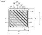
- 4 is a schematic cross-sectional view of the multilayer ceramic capacitor shown in FIG. 1, as viewed from the direction of the arrows along line IV-IV.
- 4 is a schematic cross-sectional view of the multilayer ceramic capacitor shown in FIG. 3, as viewed from the direction of the arrows along line VV.
- 6 is a schematic cross-sectional view of the multilayer ceramic capacitor shown in FIG.
- FIG. 5 is a schematic cross-sectional view for illustrating details of a side margin portion of the multilayer ceramic capacitor according to the embodiment.
- FIG. 3 is a schematic cross-sectional view for explaining details of an outer layer portion of the multilayer ceramic capacitor according to the embodiment.
- FIG. 4 is a schematic cross-sectional view for explaining details of an end margin portion and an external electrode of the multilayer ceramic capacitor according to the embodiment.
- FIG. 2 is a schematic cross-sectional view showing a detailed configuration of an external electrode of the multilayer ceramic capacitor according to the embodiment;
- FIG. 5 is a schematic cross-sectional view for explaining a shift in the width direction of an extended portion of an internal electrode layer in a multilayer ceramic capacitor according to an embodiment.
- FIG. 2 is a flow diagram showing a method for manufacturing a multilayer ceramic capacitor according to an embodiment.
- 10 is a schematic cross-sectional view for explaining details of an end margin portion and external electrodes of a multilayer ceramic capacitor according to a modified example.
- FIG. 11 is a flow chart showing a method for manufacturing a multilayer ceramic capacitor according to a modified example.
- FIG. 1 is a perspective view showing a schematic appearance of a multilayer ceramic capacitor according to an embodiment.
- FIG. 2 is a perspective view showing a schematic element part of a multilayer ceramic capacitor according to an embodiment.
- FIG. 3 is a schematic cross-sectional view of the multilayer ceramic capacitor shown in FIG. 1 as viewed from the direction of the III-III arrow.
- FIG. 4 is a schematic cross-sectional view of the multilayer ceramic capacitor shown in FIG. 1 as viewed from the direction of the IV-IV arrow.
- FIG. 5 is a schematic cross-sectional view of the multilayer ceramic capacitor shown in FIG. 3 as viewed from the direction of the V-V arrow.
- FIG. 6 is a schematic cross-sectional view of the multilayer ceramic capacitor shown in FIG. 3 as viewed from the direction of the VI-VI arrow.
- the multilayer ceramic capacitor 100 includes a body portion 110 and external electrodes.
- the multilayer ceramic capacitor 100 includes a first external electrode 120 and a second external electrode 130 as the external electrodes.
- the element body 110 has a generally rectangular parallelepiped shape.
- the element body 110 has a first main surface 111 and a second main surface 112 that face the stacking direction T, a first side surface 113 and a second side surface 114 that face the width direction W that is perpendicular to the stacking direction T, and a first end surface 115 and a second end surface 116 that face the length direction L that is perpendicular to the stacking direction T and the width direction W.
- the corners and ridges of the element body 110 are preferably rounded.
- a corner is a portion where three faces of the element body 110 intersect
- a ridge is a portion where two faces of the element body 110 intersect.
- the first external electrode 120 is provided on the first end surface 115. Specifically, the first external electrode 120 is formed over the entire first end surface 115, and is formed so as to extend from the first end surface 115 around the first main surface 111, the second main surface 112, the first side surface 113, and the second side surface 114. As shown in Figures 5 and 6, the first external electrode 120 includes an extension portion 120E that extends from the first end surface 115 to each of the first side surface 113 and the second side surface 114.
- the second external electrode 130 is provided on the second end surface 116. Specifically, the second external electrode 130 is formed over the entire second end surface 116 and is formed so as to extend from the second end surface 116 around the first main surface 111, the second main surface 112, the first side surface 113, and the second side surface 114. As shown in Figures 5 and 6, the second external electrode 130 includes an extension portion 130E that extends from the second end surface 116 to each of the first side surface 113 and the second side surface 114.
- the detailed configuration of the first external electrode 120 and the second external electrode 130 will be described later.
- the element part 110 includes a laminate 101 and a coating layer 160.
- the coating layer 160 contains Si and K.
- the laminate 101 has a pair of principal surfaces 101a, 101b facing each other in the stacking direction T, a pair of side surfaces 101c, 101d facing each other in the width direction, and a pair of end surfaces 101e, 101f facing each other in the length direction.
- the pair of principal surfaces 101a, 101b, the pair of side surfaces 101c, 101d, and the pair of end surfaces 101e, 101f are covered by a coating layer 160.
- the coating layer 160 is located on the first side surface 113, the second side surface 114, the first principal surface 111, and the second principal surface 112. At the first end surface 115 and the second end surface 116, the multiple dielectric layers 140 are covered by the coating layer 160.
- the laminate 101 has a plurality of dielectric layers 140 and a plurality of internal electrode layers 150 stacked alternately along the stacking direction T.
- the multiple internal electrode layers 150 include multiple first internal electrode layers 151 and multiple second internal electrode layers 152.
- the multiple first internal electrode layers 151 and the multiple second internal electrode layers 152 are alternately stacked in the stacking direction T.
- the multiple first internal electrode layers 151 are extended to the end face 101e.
- the multiple first internal electrode layers 151 are electrically connected to the first external electrode 120.
- the multiple second internal electrode layers 152 are extended to the end face 101f.
- the multiple second internal electrode layers 152 are electrically connected to the second external electrode 130. Both ends in the width direction W of the multiple first internal electrode layers 151 and the multiple second internal electrode layers 152 are exposed to the side faces 101c and 101d.
- first internal electrode layers 151 and seven second internal electrode layers 152 are provided in each of Figures 2 to 4, the number of each of the first internal electrode layers 151 and the second internal electrode layers 152 is not limited to seven.
- the number of the multiple internal electrode layers 150 is preferably 1 to 1000 or more.
- the thickness of the internal electrode layer 150 is preferably 0.3 ⁇ m to 0.8 ⁇ m.
- the first internal electrode layer 151 includes a first opposing portion 151C and a first drawn portion 151X.
- the first opposing portion 151C faces the adjacent second internal electrode layer 152 in the stacking direction T.
- the first drawn portion 151X connects the first opposing portion 151C and the first external electrode 120.
- the first drawn portion 151X is drawn to the first end surface 115 side.
- the first opposing portion 151C and the first drawn portion 151X are integrally configured.
- the first internal electrode layer 151 has a first narrow portion 151N on the side opposite to the side connected to the first external electrode 120 in the length direction L, the first narrow portion 151N having a width in the width direction W narrower than the central portion in the length direction L. In the width direction W, the width W2 of the first narrow portion 151N is smaller than the width W1 of the first opposing portion 151C.
- the region on the second end face 116 side of the element body 110 where adjacent internal electrode layers 150 do not overlap in the stacking direction T i.e., the region from the end on the second end face 116 side of the region where adjacent internal electrode layers 150 overlap in the stacking direction T to the second end face 116, is defined as Lgap.
- the first narrow portion 151N does not necessarily have to be formed, and the width of the portion where the first narrow portion 151N is formed may be W1. In this case, it is preferable that the length in the longitudinal direction L of the extension portion 120E of the first external electrode 120 is shorter than the length of Lgap along the longitudinal direction L, or that the extension portion 120E is not formed.
- the second internal electrode layer 152 includes a second opposing portion 152C and a second pull-out portion 152X.
- the second opposing portion 152C faces the adjacent first internal electrode layer 151 in the stacking direction T.
- the second pull-out portion 152X connects the second opposing portion 152C and the second external electrode 130.
- the second pull-out portion 152X is pulled out to the second end surface 116 side.
- the second opposing portion 152C and the second pull-out portion 152X are integrally configured.
- the second internal electrode layer 152 has a second narrow portion 152N on the side opposite to the side connected to the second external electrode 130 in the length direction L, the second narrow portion 152N having a width in the width direction W narrower than the central portion in the length direction L.
- the width W4 of the second narrow portion 152N is smaller than the width W3 of the second opposing portion 152C.
- the region on the first end face 115 side of the element body 110 where adjacent internal electrode layers 150 do not overlap in the stacking direction T i.e., the region from the end on the first end face 115 side of the region where adjacent internal electrode layers 150 overlap in the stacking direction T to the first end face 115, is defined as Lgap.
- the second narrow portion 152N does not necessarily have to be formed, and the width of the portion where the second narrow portion 152N is formed may be W3. In this case, it is preferable that the length in the longitudinal direction L of the extension portion 130E of the second external electrode 130 is shorter than the length of Lgap along the longitudinal direction L, or that the extension portion 130E is not formed.
- Each of the first internal electrode layer 151 and the second internal electrode layer 152 contains one metal selected from the group consisting of Ni, Cu, Ag, Pd, and Au, or an alloy containing the metal.
- each of the first internal electrode layer 151 and the second internal electrode layer 152 contains Ni as a main component.
- Each of the first internal electrode layer 151 and the second internal electrode layer 152 may further contain dielectric particles of the same composition as the ceramic contained in the dielectric layer 140.
- each of the first internal electrode layer 151 and the second internal electrode layer 152 may contain Sn at the interface with the dielectric layer 140.
- the multiple dielectric layers 140 are composed of outer layer dielectric layers located between the internal electrode layer 150 located closest to the first main surface 111 in the stacking direction T and the first main surface 111, and between the internal electrode layer 150 located closest to the second main surface 112 in the stacking direction T and the second main surface 112, and inner layer dielectric layers located between the internal electrode layers 150 adjacent to each other in the stacking direction T.
- the number of the multiple dielectric layers 140 is preferably 100 to 1000.
- the thickness of the dielectric layer 140 is preferably 0.4 ⁇ m to 0.8 ⁇ m.
- Each of the plurality of dielectric layers 140 may be made of a ceramic material such as a dielectric ceramic containing components such as BaTiO3 , CaTiO3 , SrTiO3 , or CaZrO3 .
- a component such as a Mn compound, an Fe compound, a Cr compound, a Co compound, or a Ni compound may be added to the main components.
- the element body 110 is divided into an inner layer C, a first outer layer X1 and a second outer layer X2, a first side margin S1 and a second side margin S2, and a first end margin E1 and a second end margin E2.
- the inner layer C has a capacitance due to the stacking in the stacking direction T of a first opposing portion 151C (described later) of the first internal electrode layer 151 and a second opposing portion 152C (described later) of the second internal electrode layer 152.
- the first outer layer portion X1 and the second outer layer portion X2 sandwich the inner layer portion C in the stacking direction T.
- the first outer layer portion X1 is located outside the inner layer portion C in the stacking direction T, and is located on the first main surface 111 side. In other words, the first outer layer portion X1 is located closer to the first main surface 111 than the internal electrode layer 150 located closest to the first main surface 111 in the stacking direction T.
- the second outer layer portion X2 is located outside the inner layer portion C in the stacking direction T, and is located on the second main surface 112 side. In other words, the second outer layer portion X2 is located closer to the second main surface 112 than the internal electrode layer 150 located closest to the second main surface 112 in the stacking direction T.
- Each of the first outer layer X1 and the second outer layer X2 extends in the length direction L and the width direction W so as to include the ridge portion of the element body 110. It is preferable that each of the first outer layer X1 and the second outer layer X2 has a thickness of 10 ⁇ m or more and 30 ⁇ m or less.
- Each of the first outer layer portion X1 and the second outer layer portion X2 includes an outermost layer portion disposed on the outermost side and an inner outer layer portion located inside the outermost layer portion.
- the outermost layer portion is composed of the coating layer 160.
- the inner outer layer portion is composed of an outer dielectric layer.
- the first end margin portion E1 and the second end margin portion E2 sandwich the inner layer portion C in the longitudinal direction L.
- the first end margin portion E1 is located outside the inner layer portion C in the longitudinal direction L, and is located on the first end face 115 side.
- the second end margin portion E2 is located outside the inner layer portion C in the longitudinal direction L, and is located on the second end face 116 side.
- the side margin portion is located in the element body portion 110 between the first side surface 113 and the multiple internal electrode layers 150, and between the second side surface 114 and the multiple internal electrode layers 150 in the width direction W.
- the side margin portion is composed of a coating layer 160.
- the coating layer 160 covers both ends of the multiple internal electrode layers 150 in the width direction W.
- the first side margin portion S1 is provided on the side surface 101c of the laminate.
- the first side margin portion S1 is provided so as to cover the entire side surface 101c.
- the first side margin portion S1 exists in the element portion 110 from one end portion of the internal electrode layer 150 located on one side in the width direction W to the first side surface 113.
- the covering layer 160 is formed on one end portion in the width direction W of the center portion in the length direction L of each of the multiple internal electrode layers 150.
- the second side margin portion S2 is provided on the side surface 101d of the laminate.
- the second side margin portion S2 is provided so as to cover the entire side surface 101d.
- the second side margin portion S2 exists in the element portion 110 from the other end portion of the internal electrode layer 150 located on the other side of the width direction W to the second side surface 114.
- a covering layer 160 is formed on the other end portion in the width direction W of the center portion in the length direction L of each of the multiple internal electrode layers 150.
- the size of the multilayer ceramic capacitor 100 including the body 110, the first external electrode 120, and the second external electrode 130 is not particularly limited, but may be within the following range, for example:
- the dimension in the length direction L of the multilayer ceramic capacitor 100 is, for example, 0.1 mm or more and 3.2 mm or less.
- the dimension in the stacking direction T of the multilayer ceramic capacitor 100 is, for example, 0.05 mm or more and 1.6 mm or less.
- the dimension in the width direction W of the multilayer ceramic capacitor 100 is, for example, 0.05 mm or more and 1.6 mm or less.
- the multilayer ceramic capacitor 100 has, for example, a length dimension L0 of 0.1 mm, a width dimension W0 of 0.05 mm, and a thickness dimension T0 of 0.05 mm, or a length dimension L0 of 0.6 mm, a width dimension W0 of 0.3 mm, and a thickness dimension T0 of 0.3 mm, or a length dimension L0 of 1.0 mm, a width dimension W0 of 0.5 mm, and a thickness dimension T0 of 0.5 mm, or a length dimension L0 of 1.6 mm, a width dimension W0 of 0.8 mm, and a thickness dimension T0 of 0.8 mm, or a length dimension L0 of 3.2 mm, a width dimension W0 of 1.6 mm, and a thickness dimension T0 of 1.6 mm. Note that tolerances are taken into account in the above sizes.
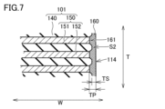
- FIG. 7 is a schematic cross-sectional view for explaining the details of a side margin portion of a multilayer ceramic capacitor according to an embodiment.
- FIG. 7 shows a cross-section of the element body 110 parallel to the stacking direction T and width direction W on the second side surface 114 side.
- the second side margin portion S2 side will be explained, but the same applies to the first side margin portion S1 side.
- the second side margin portion S2 is composed of a coating layer 160 containing Si and K.
- the composition of the coating layer 160 can be confirmed by EDX (Energy dispersive X-ray spectroscopy).
- the coating layer 160 is amorphous, and the fact that the coating layer 160 is amorphous can be confirmed by Raman spectroscopy.
- the fact that no specific crystal pattern can be detected by X-ray diffraction of the coating layer 160 also confirms that the coating layer 160 is amorphous.
- the second side margin portion S2 protrudes so as to contact the ends of the multiple internal electrode layers 150 in the width direction W.
- a part 161 of the covering layer 160 covering both ends of the multiple internal electrode layers 150 in the width direction W is sandwiched between adjacent dielectric layers 140 in the stacking direction T among the multiple dielectric layers 140.
- the reason for this shape is that the shrinkage rate of the internal electrode layer 150 is greater than the shrinkage rate of the dielectric layer 140 during firing.
- This shape of the side margin portion can increase the adhesive strength of the side margin portion to the side surfaces 101c, 101d of the laminate 101. As a result, peeling of the side margin portion can be suppressed.
- the minimum thickness TS of the coating layer 160 located on the ends of the multiple internal electrode layers 150 in the width direction W is 0.01 ⁇ m or more and 10 ⁇ m or less. From the viewpoint of moisture resistance, it is more preferable that the minimum thickness TS is 0.1 ⁇ m or more, and even more preferable that it is 0.3 ⁇ m or more.
- the shortest distance TP between the multiple internal electrode layers 150 and the first side surface S1, and the shortest distance TP between the multiple internal electrode layers 150 and the second side surface S2 is 0.01 ⁇ m or more and 10 ⁇ m or less. From the viewpoint of moisture resistance, it is more preferable that the shortest distance TP is 0.1 ⁇ m or more, and even more preferable that it is 0.3 ⁇ m or more.
- the numerical ranges of the minimum thickness TS and the shortest distance TP are not limited to the above.
- the above-mentioned shape and thickness relationship explained using FIG. 7 can be confirmed by polishing the element body 110 from the first external electrode 120 side to the center in the length direction L, and observing a cross section of the element body 110 parallel to the stacking direction T and width direction W using an electron microscope or the like.
- the minimum thickness TS is the thickness of the thinnest coating layer 160 measured in an image taken with a SEM (Scanning Electron Microscope) in a range where about 10 first internal electrode layers 151 or second internal electrode layers 152 are included in the field of view at the center in the stacking direction T of the cross section.
- the shortest distance TP is the shortest distance measured between the internal electrode layer 150 and the first side surface S1 or the second side surface S2 in the image.
- FIG. 8 is a schematic cross-sectional view for explaining the details of the outer layer portion of the multilayer ceramic capacitor according to the embodiment.
- FIG. 8 shows a cross-section of the element body 110 parallel to the stacking direction T and width direction W on the first outer layer portion X1 side.
- the first outer layer portion X1 side will be explained, but the same applies to the second outer layer portion X2 side.
- the first outer layer portion X1 includes an outermost layer portion Xa disposed on the outermost side, and an inner outer layer portion Xb located inside the outermost layer portion Xa.
- the outermost layer portion Xa is composed of a coating layer 160.
- the inner outer layer portion Xb is composed of an outer dielectric layer 140.
- the outer surface of the inner outer layer Xb has fine irregularities due to the dielectric grains of the outer dielectric layer 140.
- the coating layer 160 is amorphous and covers the inner outer layer Xb so as to fill in the irregularities on the outer surface of the inner outer layer Xb, so there are almost no irregularities on the outer surface of the outermost layer Xa. Therefore, the maximum height Ha of the irregularities on the outer surface of the outermost layer Xa is smaller than the maximum height Hb of the irregularities on the outer surface of the inner outer layer Xb. This improves the impact resistance of the outermost layer Xa and suppresses a decrease in the moisture resistance of the multilayer ceramic capacitor 100.
- the minimum thickness TM of the coating layer 160 in the stacking direction T in each of the first outer layer portion X1 and the second outer layer portion X2 is 0.01 ⁇ m or more and 0.5 ⁇ m or less. Note that the numerical range of the minimum thickness TM is not limited to the above.
- the relationship between the shape and thickness described above using FIG. 8 can be confirmed by polishing the element body 110 from the first external electrode 120 side to the center in the length direction L, and observing a cross section of the element body 110 parallel to the stacking direction T and width direction W using an electron microscope or the like.
- the minimum thickness TM is the thinnest thickness in the stacking direction T of the coating layer 160 measured in an image taken with a SEM (Scanning Electron Microscope) in the range where the first outer layer X1 or the second outer layer X2 is visible at the end of the stacking direction T of the cross section.
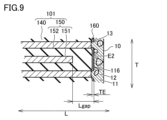
- FIG. 9 is a schematic cross-sectional view for explaining the details of the end margin portion and external electrodes of a multilayer ceramic capacitor according to an embodiment.
- FIG. 9 shows a cross-section of the element body 110 parallel to the stacking direction T and length direction L on the second end margin portion E2 side.
- the second end margin portion E2 side will be explained, but the same applies to the first end margin portion E1 side.
- the external electrode includes a Cu layer 10 containing a Cu component 11 as a main component and a glass component 12.
- the composition of the Cu layer 10 can be confirmed by EDX.
- a coating layer 160 is disposed on the second end face 116, and a part 13 of the Cu layer 10 penetrates the coating layer 160 and is electrically connected to the second internal electrode layer 152.
- the coating layer 160 is located between the multiple dielectric layers 140 and the external electrode. Specifically, the coating layer 160 is located between the multiple dielectric layers 140 and the Cu layer 10.
- the thickness of the Cu layer 10 is 30 ⁇ m or more and 100 ⁇ m or less at the center in the stacking direction T and the width direction W.
- the numerical range of the thickness of the Cu layer 10 is not limited to the above.
- the Cu layer 10 may be a resin layer containing a Cu component and a glass component. In this case, a base metal layer is formed between the resin layer and the coating layer 160.
- the minimum thickness TS of the coating layer 160 located on the ends of the multiple internal electrode layers 150 in the width direction W shown in FIG. 7 is thicker than the minimum thickness TE of the coating layer 160 located between the multiple dielectric layers 140 and the Cu layer 10, which is the external electrode, shown in FIG. 9.
- the relationship between the shape and thickness described above using FIG. 9 can be confirmed by polishing the element part 110 from the first side surface 113 side to the center in the width direction W, and observing a cross section of the element part 110 parallel to the stacking direction T and the length direction L using an electron microscope or the like.
- the minimum thickness TE is the thickness of the thinnest coating layer 160 measured in an image taken by SEM in a range that includes about 10 first internal electrode layers 151 or second internal electrode layers 152 at the center in the stacking direction T and the end in the length direction L of the cross section.
- the reason for the shape shown in FIG. 9 is that the coating layer 160 contains K, which lowers the melting point of the Si contained in the coating layer 160 to below the firing temperature of the Cu layer 10. Therefore, when the Cu layer 10 is fired, the coating layer 160 melts and the contraction force of the Cu layer 10 acts on the molten coating layer 160, so that a portion 13 of the Cu layer 10 penetrates the coating layer 160 and connects to the second internal electrode layer 152.
- the K contained in the coating layer 160 flows and diffuses into the glass component 12 in the Cu layer 10. That is, the glass component 12 contains K. The closer to the second end face 116, the higher the concentration of K contained in the glass component 12.
- some of the Si contained in the coating layer 160 penetrates into the Cu layer 10 so as to bond with the glass component 12 in the Cu layer 10.
- Cu diffuses from the Cu layer 10 into the Ni of the internal electrode layer 150. This increases the adhesive strength between the Cu layer 10 and the internal electrode layer 150. As a result, peeling of the first external electrode 120 and the second external electrode 130 can be suppressed.
- the Si concentration of the coating layer 160 located on the ends of the multiple internal electrode layers 150 in the width direction W shown in FIG. 7 is higher than the Si concentration of the coating layer 160 located between the multiple dielectric layers 140 and the external electrodes shown in FIG. 9.
- the K concentration of the coating layer 160 located on the ends of the multiple internal electrode layers 150 in the width direction W shown in FIG. 7 is higher than the K concentration of the coating layer 160 located between the multiple dielectric layers 140 and the external electrodes shown in FIG. 9.
- the concentration distribution of Si and K may be observed from images captured by a TEM (Transmission Electron Microscope) or EDX.
- TEM Transmission Electron Microscope
- EDX EDX
- the concentration gradient of Si and K is measured by the TEM as a molar ratio relative to 100 mol of Ti contained in the dielectric layer 140.
- the above-described configuration of the coating layer 160 and the external electrode ensures moisture resistance through the thin side margins, while ensuring electrical connection between the internal electrode layer 150 and the external electrode without removing the coating layer 160 on the first end face 115 and the second end face 116 by sandblasting or the like. This in turn expands the area in which the internal electrode layer 150 can be arranged, thereby enabling the multilayer ceramic capacitor 100 to be made smaller and have a larger capacity.
- FIG. 10 is a schematic cross-sectional view showing the detailed configuration of the external electrodes of the multilayer ceramic capacitor according to the embodiment.
- FIG. 10 shows a cross-section of the element body 110 parallel to the stacking direction T and length direction L on the second external electrode 130 side.
- the second external electrode 130 side will be described, but the same applies to the first external electrode 120 side.
- the first external electrode 120 and the second external electrode 130 include a Cu layer 10 provided on the element body 110, a Ni plating layer 20 provided on the Cu layer 10, and a Sn plating layer 30 provided on the Ni plating layer 20.
- the material constituting the plating layer may be one metal selected from the group consisting of Ni, Cu, Ag, Pd, and Au, or an alloy containing the metal.
- the total thickness of the Ni plating layer 20 and the Sn plating layer 30 is, for example, 3 ⁇ m or more and 20 ⁇ m or less.
- the extension portion 120E when viewed in the width direction W, overlaps only the narrow portion 152N with the second internal electrode layer 152, which is not electrically connected to the first external electrode 120 including the extension portion 120E, among the multiple internal electrode layers 150.
- the extension portion 130E when viewed in the width direction W, overlaps only the narrow portion 151N with the first internal electrode layer 151, which is not electrically connected to the second external electrode 130 including the extension portion 130E, among the multiple internal electrode layers 150.
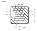
- FIG. 11 is a schematic cross-sectional view for explaining the widthwise misalignment of the extensions of the internal electrode layers in a multilayer ceramic capacitor according to an embodiment. Note that FIG. 11 is illustrated for the sake of convenience in explaining the amount of misalignment of the extensions, and the position of the extensions is not limited to the aspect shown in FIG. 11.
- the misalignment amount D1 in the width direction W between the extension portion 130E located closest to the first side surface 113 and the extension portion 130E located closest to the second side surface 114 is 3 ⁇ m or more.
- the above-mentioned misalignment amount in the multiple extension portions 120E is the same as that of the extension portion 130E. In this way, the ends in the width direction W of the multiple extension portions 120E and the multiple extension portions 130E are not aligned in the stacking direction T, but are misaligned in the width direction W.
- the misalignment in the width direction W of the internal electrode layers 150 adjacent to each other in the stacking direction T is less than 3 ⁇ m.
- the amount of misalignment in the width direction W of the first narrow portion 151N and the second narrow portion 152N is greater than the amount of misalignment in the width direction W of the center portion of the length direction L of the multiple internal electrode layers 150.
- the width of the first narrow portion 151N and the second narrow portion 152N is equal to or greater than the expected maximum positional deviation in the width direction W of the first narrow portion 151N and the second narrow portion 152N, and is narrower than the width of the center portion in the length direction L of the multiple internal electrode layers 150.
- Figure 12 is a flow diagram showing the method for manufacturing the multilayer ceramic capacitor according to this embodiment.
- a ceramic dielectric slurry is prepared (step S1). Specifically, ceramic dielectric powder, additive powder, binder resin, and dissolving liquid are dispersed and mixed, and thus a ceramic dielectric slurry is prepared.
- the ceramic dielectric powder is, for example, BaTiO 3 , CaTiO 3 , SrTiO 3 , CaZrO 3 , or CaHfO 3 dielectric particles having a perovskite structure.
- the additive powder is, for example, at least one of a Si compound, an Mg compound, an Mn compound, an Fe compound, a Cr compound, an Ni compound, and a Co compound.
- the binder resin polyurethane resin, urea resin, melamine resin, epoxy resin, vinyl acetate resin, acrylic resin, or an aqueous polymer such as polyvinyl alcohol (PVA) or polyvinyl butyral (PVB) can be used. These may be used alone or in a mixture of two or more kinds.
- the ceramic dielectric slurry may be either a solvent-based or water-based. When the ceramic dielectric slurry is a water-based paint, the ceramic dielectric slurry is prepared by mixing a water-soluble binder, a dispersant, etc. with a dielectric raw material dissolved in water.
- a ceramic dielectric sheet is formed (step S2). Specifically, the ceramic dielectric slurry is formed into a sheet shape on a carrier film using a die coater, gravure coater, or microgravure coater, and then dried to form a ceramic dielectric sheet. From the viewpoint of miniaturization and high capacity of the multilayer ceramic capacitor, the thickness of the ceramic dielectric sheet is preferably 0.4 ⁇ m or more and 0.8 ⁇ m or less.
- a mother sheet is formed (step S3). Specifically, a ceramic dielectric sheet is coated with a conductive paste in a predetermined pattern, thereby forming a mother sheet on which a predetermined internal electrode pattern is provided.
- the conductive paste contains Ni powder, a solvent, a dispersant, a binder, and the like, and is prepared so as to have a constant viscosity.
- Polyvinyl butyral (PVB) or polyvinyl alcohol (PVA) is used as the binder.
- the conductive paste can be coated by screen printing, inkjet printing, gravure printing, or the like.
- the thickness of the internal electrode pattern is preferably 0.3 ⁇ m or more and 0.8 ⁇ m or less.
- a ceramic dielectric sheet that has not been subjected to the above step S3 is also prepared as the mother sheet.
- multiple mother sheets are stacked (step S4). Specifically, a predetermined number of mother sheets that do not have an internal electrode pattern and are made of ceramic dielectric sheets only are stacked to a thickness of, for example, 10 ⁇ m or more and 30 ⁇ m or less. A predetermined number of mother sheets with internal electrode patterns are stacked on top of these. The number of mother sheets with internal electrode patterns stacked is, for example, 1 sheet or more and 1000 sheets or less. A predetermined number of mother sheets that do not have an internal electrode pattern and are made of ceramic dielectric sheets only are stacked on top of these to a thickness of, for example, 10 ⁇ m or more and 30 ⁇ m or less. This forms a mother sheet group.
- the group of mother sheets is pressed together to form a dielectric block (step S5).
- the group of mother sheets is pressed in the stacking direction by a hydrostatic press or a rigid press to form the dielectric block.
- the ceramic dielectric sheets are pressed at a predetermined temperature, so that the ceramic dielectric sheets adhere to each other.
- a ceramic dielectric sheet of a certain thickness on the outermost layer in the stacking direction and pressing it, it is possible to protect the dielectric sheet on which the internal electrode pattern is formed.
- the dielectric block is divided to form chips (step S6). Specifically, the dielectric block is divided into a matrix shape by pressing, dicing or laser cutting, and is separated into a plurality of chips. When dividing the dielectric block, the dielectric block may be divided in a state in which it is softened by heating.
- the chip is fired (step S7). Specifically, the chip is heated, which fires the dielectric material and conductive material contained in the chip, forming the laminate 101.
- the firing temperature is set appropriately according to the dielectric material and conductive material.
- a coating layer 160 is formed on the fired chip (step S8).
- the fired laminate 101 is immersed in a solution containing Si and K, and then dried.
- the solution is, for example, water glass containing K.
- a paste that will become the Cu layer 10 is applied to the chip (step S9). Specifically, a paste containing Cu particles and a glass component is applied to each of the first end face 115 and the second end face 116 of the dried element body 110, and then dried.
- step S10 the chip coated with the paste that will become the Cu layer 10 is fired (step S10).
- the element part 110 coated with the paste that will become the Cu layer 10 is fired at a temperature of 600°C or higher and 800°C or lower.
- the metal components contained in the paste that will become the Cu layer 10 are sintered, the coating layer 160 melts, and the first internal electrode layer 151 and the Cu layer 10 are electrically connected at the first end surface 115, and the second internal electrode layer 152 and the Cu layer 10 are electrically connected at the second end surface 116.
- step S11 the external electrodes are formed (step S11).
- the Cu layer 10 is Ni-plated and Sn-plated in this order to form the Ni-plated layer 20 and the Sn-plated layer 30, thereby forming the first external electrode 120 and the second external electrode 130.
- the multilayer ceramic capacitor 100 according to the embodiment can be manufactured.
- the multilayer ceramic capacitor according to the modified example differs from the multilayer ceramic capacitor 100 according to this embodiment mainly in that a base electrode layer containing Ni as a main component is formed on the first end face 115 and the second end face 116 of the element body 110, and therefore a description of the configuration that is the same as that of the multilayer ceramic capacitor 100 according to this embodiment will not be repeated.
- FIG. 13 is a schematic cross-sectional view for explaining the details of the end margin portion and external electrodes of a multilayer ceramic capacitor according to a modified example.
- FIG. 13 shows a cross-section of the element body 110 parallel to the stacking direction T and length direction L on the second end margin portion E2 side.
- the second end margin portion E2 side will be explained, but the same applies to the first end margin portion E1 side.
- the external electrode includes a base electrode layer 40 containing Ni as a main component, and a Cu layer 10 containing a Cu component 11 as a main component and a glass component 12.
- the base electrode layer 40 may further contain dielectric particles of the same composition as the ceramic contained in the dielectric layer 140.
- a base electrode layer 40 is formed on the second end surface 116, a coating layer 160 is formed on the base electrode layer 40, and a Cu layer 10 is formed on the coating layer 160.
- the base electrode layer 40 is covered with the Cu layer 10.
- the minimum thickness TS of the coating layer 160 located on the ends of the multiple internal electrode layers 150 in the width direction W shown in FIG. 7 is thicker than the minimum thickness TF of the coating layer 160 located between the base electrode layer 40 and the Cu layer 10 shown in FIG. 13.
- a portion 13 of the Cu layer 10 penetrates the coating layer 160 and is electrically connected to the base electrode layer 40.
- the Cu layer 10 is electrically connected to the second internal electrode layer 152 via the base electrode layer 40.
- the base electrode layer 40 is formed so as to wrap around from the second end face 116 to the first main surface 111, the second main surface 112, the first side surface 113, and the second side surface 114. Similarly, the base electrode layer 40 is formed so as to wrap around from the first end face 115 to the first main surface 111, the second main surface 112, the first side surface 113, and the second side surface 114.
- the Cu layer 10 and the second internal electrode layer 152 are electrically connected via the base electrode layer 40 that covers the entire second end face 116, so that the second internal electrode layer 152 and the second external electrode 130 can be stably electrically connected.
- the Cu layer 10 and the first internal electrode layer 151 are electrically connected via the base electrode layer 40 that covers the entire first end face 115, so that the first internal electrode layer 151 and the first external electrode 120 can be stably electrically connected.
- the K contained in the coating layer 160 flows and diffuses into the glass component 12 in the Cu layer 10. Some of the Si contained in the coating layer 160 penetrates into the Cu layer 10 so as to bond with the glass component 12 in the Cu layer 10. Cu diffuses from the Cu layer 10 into the Ni of the base electrode layer 40. This increases the adhesion between the Cu layer 10 and the base electrode layer 40. This in turn makes it possible to suppress peeling of the first external electrode 120 and the second external electrode 130.
- Figure 14 is a flow diagram showing the method for manufacturing the multilayer ceramic capacitor according to the modified example.
- the manufacturing method of the multilayer ceramic capacitor according to the modified example is similar to steps S1 to S6 of the manufacturing method of the multilayer ceramic capacitor 100.
- step S6 a paste that will become the base electrode layer is applied to the chip (step S17). Specifically, a paste containing Ni particles is applied to each of end faces 101e and 101f of the laminate 101, and then dried.
- step S18 the chip coated with the paste that will become the base electrode layer 40 is fired (step S18). Specifically, the chip is heated, which fires the paste containing Ni particles along with the dielectric material and conductive material contained in the chip, forming the laminate 101 and the base electrode layer 40.
- a coating layer 160 is formed on the chip on which the base electrode layer 40 is formed (step S19). Specifically, the laminate 101 on which the base electrode layer 40 is formed is immersed in a solution containing Si and K, and then dried.
- the solution is, for example, water glass containing K.
- a paste that will become the Cu layer 10 is applied to the chip (step S20). Specifically, a paste containing Cu particles and a glass component is applied so as to cover the base electrode layer 40 of each of the first end face 115 and the second end face 116 via the coating layer 160, and then dried.
- step S21 the chip coated with the paste that will become the Cu layer 10 is fired (step S21). Specifically, the chip coated with the paste that will become the Cu layer 10 is fired at a temperature of 600°C or higher and 800°C or lower. As a result, the metal components contained in the paste that will become the Cu layer 10 are sintered, the coating layer 160 melts, and the base electrode layer 40 and the Cu layer 10 are electrically connected.
- the Cu layer 10 is Ni-plated and Sn-plated in this order to form the Ni-plated layer 20 and the Sn-plated layer 30, thereby forming the first external electrode 120 and the second external electrode 130.
- the multilayer ceramic capacitor according to the modified example can be manufactured.
Landscapes
- Engineering & Computer Science (AREA)
- Power Engineering (AREA)
- Manufacturing & Machinery (AREA)
- Microelectronics & Electronic Packaging (AREA)
- Fixed Capacitors And Capacitor Manufacturing Machines (AREA)
- Ceramic Capacitors (AREA)
Priority Applications (2)
| Application Number | Priority Date | Filing Date | Title |
|---|---|---|---|
| CN202480042411.9A CN121399708A (zh) | 2023-11-22 | 2024-10-09 | 层叠陶瓷电容器 |
| JP2025559083A JPWO2025109892A1 (https=) | 2023-11-22 | 2024-10-09 |
Applications Claiming Priority (2)
| Application Number | Priority Date | Filing Date | Title |
|---|---|---|---|
| JP2023198282 | 2023-11-22 | ||
| JP2023-198282 | 2023-11-22 |
Publications (1)
| Publication Number | Publication Date |
|---|---|
| WO2025109892A1 true WO2025109892A1 (ja) | 2025-05-30 |
Family
ID=95826555
Family Applications (1)
| Application Number | Title | Priority Date | Filing Date |
|---|---|---|---|
| PCT/JP2024/036064 Pending WO2025109892A1 (ja) | 2023-11-22 | 2024-10-09 | 積層セラミックコンデンサ |
Country Status (3)
| Country | Link |
|---|---|
| JP (1) | JPWO2025109892A1 (https=) |
| CN (1) | CN121399708A (https=) |
| WO (1) | WO2025109892A1 (https=) |
Citations (4)
| Publication number | Priority date | Publication date | Assignee | Title |
|---|---|---|---|---|
| JP2003151805A (ja) * | 2001-11-15 | 2003-05-23 | Murata Mfg Co Ltd | チップ型電子部品およびその製造方法 |
| JP2010080703A (ja) * | 2008-09-26 | 2010-04-08 | Tdk Corp | セラミック積層電子部品およびその製造方法 |
| WO2020241122A1 (ja) * | 2019-05-24 | 2020-12-03 | 株式会社村田製作所 | 表面改質ガラス、電子部品、及び、ケイ酸塩皮膜の形成方法 |
| WO2023084878A1 (ja) * | 2021-11-09 | 2023-05-19 | 株式会社村田製作所 | 電子部品 |
-
2024
- 2024-10-09 JP JP2025559083A patent/JPWO2025109892A1/ja active Pending
- 2024-10-09 WO PCT/JP2024/036064 patent/WO2025109892A1/ja active Pending
- 2024-10-09 CN CN202480042411.9A patent/CN121399708A/zh active Pending
Patent Citations (4)
| Publication number | Priority date | Publication date | Assignee | Title |
|---|---|---|---|---|
| JP2003151805A (ja) * | 2001-11-15 | 2003-05-23 | Murata Mfg Co Ltd | チップ型電子部品およびその製造方法 |
| JP2010080703A (ja) * | 2008-09-26 | 2010-04-08 | Tdk Corp | セラミック積層電子部品およびその製造方法 |
| WO2020241122A1 (ja) * | 2019-05-24 | 2020-12-03 | 株式会社村田製作所 | 表面改質ガラス、電子部品、及び、ケイ酸塩皮膜の形成方法 |
| WO2023084878A1 (ja) * | 2021-11-09 | 2023-05-19 | 株式会社村田製作所 | 電子部品 |
Also Published As
| Publication number | Publication date |
|---|---|
| JPWO2025109892A1 (https=) | 2025-05-30 |
| CN121399708A (zh) | 2026-01-23 |
Similar Documents
| Publication | Publication Date | Title |
|---|---|---|
| US20240312712A1 (en) | Electronic component | |
| JP6852253B2 (ja) | 積層セラミック電子部品及びその製造方法 | |
| KR101971870B1 (ko) | 전자부품의 제조 방법 | |
| US10896781B2 (en) | Ceramic capacitor having metal or metal oxide in side margin portions, and method of manufacturing the same | |
| JP7359258B2 (ja) | 積層セラミック電子部品、及び、積層セラミック電子部品の製造方法 | |
| US11610734B2 (en) | Multilayer ceramic capacitor and method of manufacturing the same | |
| US20110267736A1 (en) | Electronic component | |
| KR20190121144A (ko) | 적층 세라믹 커패시터 및 그 제조 방법 | |
| JP2018022832A (ja) | 電子部品 | |
| JP2018022833A (ja) | 電子部品 | |
| JP4840392B2 (ja) | 積層コンデンサ | |
| WO2025109892A1 (ja) | 積層セラミックコンデンサ | |
| KR20130027784A (ko) | 외부 전극용 도전성 페이스트, 이를 이용한 적층 세라믹 전자부품 및 이의 제조방법 | |
| WO2025109816A1 (ja) | 積層セラミックコンデンサ | |
| WO2025109818A1 (ja) | 積層セラミックコンデンサ | |
| WO2025109893A1 (ja) | 積層セラミックコンデンサ | |
| WO2025109817A1 (ja) | 積層セラミックコンデンサ | |
| KR101938558B1 (ko) | 적층 세라믹 전자부품 | |
| JP7188345B2 (ja) | 積層セラミック電子部品の製造方法 | |
| KR20260053068A (ko) | 적층 세라믹 콘덴서 | |
| KR20260057666A (ko) | 적층 세라믹 콘덴서 | |
| JP7707010B2 (ja) | 積層セラミックコンデンサ | |
| JP2025009367A (ja) | 積層セラミックコンデンサ | |
| JPH09129482A (ja) | 積層セラミックコンデンサの製造方法 | |
| KR20250170137A (ko) | 적층 세라믹 전자부품 |
Legal Events
| Date | Code | Title | Description |
|---|---|---|---|
| 121 | Ep: the epo has been informed by wipo that ep was designated in this application |
Ref document number: 24893886 Country of ref document: EP Kind code of ref document: A1 |
|
| ENP | Entry into the national phase |
Ref document number: 2025559083 Country of ref document: JP Kind code of ref document: A |
|
| WWE | Wipo information: entry into national phase |
Ref document number: 2025559083 Country of ref document: JP |