WO2025083865A1 - ヒートポンプ装置および駆動回路 - Google Patents
ヒートポンプ装置および駆動回路 Download PDFInfo
- Publication number
- WO2025083865A1 WO2025083865A1 PCT/JP2023/037965 JP2023037965W WO2025083865A1 WO 2025083865 A1 WO2025083865 A1 WO 2025083865A1 JP 2023037965 W JP2023037965 W JP 2023037965W WO 2025083865 A1 WO2025083865 A1 WO 2025083865A1
- Authority
- WO
- WIPO (PCT)
- Prior art keywords
- semiconductor switching
- operation mode
- drive
- frequency
- switching element
- Prior art date
- Legal status (The legal status is an assumption and is not a legal conclusion. Google has not performed a legal analysis and makes no representation as to the accuracy of the status listed.)
- Pending
Links
Images



Classifications
-
- F—MECHANICAL ENGINEERING; LIGHTING; HEATING; WEAPONS; BLASTING
- F25—REFRIGERATION OR COOLING; COMBINED HEATING AND REFRIGERATION SYSTEMS; HEAT PUMP SYSTEMS; MANUFACTURE OR STORAGE OF ICE; LIQUEFACTION SOLIDIFICATION OF GASES
- F25B—REFRIGERATION MACHINES, PLANTS OR SYSTEMS; COMBINED HEATING AND REFRIGERATION SYSTEMS; HEAT PUMP SYSTEMS
- F25B1/00—Compression machines, plants or systems with non-reversible cycle
Definitions
- This disclosure relates to a heat pump device having a compressor and a drive circuit used in the heat pump device.
- Patent Document 1 discloses a technology in which a high-frequency voltage is supplied to a motor by causing an inverter to perform switching operations at a higher frequency than during normal operation based on a high-frequency voltage command value and a carrier signal that are higher in frequency than the operating frequency during compression operation of the compressor, thereby generating iron loss and copper loss in the motor and heating the refrigerant that has become stagnant in the compressor.
- the inverter performs switching operations at high frequencies, which can increase the amount of noise generated.
- the present disclosure has been made to solve the problems described above, and aims to provide a heat pump device and drive circuit that can suppress an increase in noise during refrigerant heating operations.
- the heat pump device of the present disclosure is a heat pump having a normal operation mode and a heating operation mode, and includes a compression mechanism that compresses a refrigerant, a motor that drives the compression mechanism, an inverter that includes multiple semiconductor switching elements and applies a voltage to the motor, and a drive circuit that drives the multiple semiconductor switching elements
- the normal operation mode is an operation mode in which the motor drives the compression mechanism
- the heating operation mode is an operation mode in which the motor heats the refrigerant by generating losses without driving the compression mechanism
- the multiple semiconductor switching elements include at least one target semiconductor switching element
- the drive circuit drives the multiple semiconductor switching elements so that the switching speed of the target semiconductor switching element in the heating operation mode is lower than the switching speed of the target semiconductor switching element in the normal operation mode.
- the heat pump device and drive circuit disclosed herein can suppress an increase in noise during refrigerant heating operations.
- FIG. 1 is a diagram showing a configuration example of a heat pump device according to an embodiment.
- FIG. 2 is a block diagram showing an example of a hardware configuration in the case where at least a part of the functions of the control device in the heat pump device according to the embodiment is realized by software.
- FIG. 3 is a diagram illustrating an example of the configuration of a drive circuit in the heat pump device according to the embodiment.
- FIG. 4 is a diagram showing an example of switching waveforms of semiconductor switching elements when the driving capability of the driving circuit in the heat pump apparatus according to the embodiment is high.
- FIG. 5 is a diagram showing an example of switching waveforms of a semiconductor switching element when the driving capability of a driving circuit in a heat pump apparatus according to an embodiment is low.
- FIG. 1 is a diagram showing a configuration example of a heat pump device according to an embodiment.
- FIG. 2 is a block diagram showing an example of a hardware configuration in the case where at least a part of the functions of the control device in the heat pump device according to
- FIG. 6 is a diagram showing a schematic diagram of the relationship between a trapezoidal pulse wave and a frequency spectrum.
- FIG. 7 is a flowchart showing an outline of the operation of the control device in the heat pump device according to the embodiment.
- FIG. 8 is a diagram showing a schematic relationship between the operation mode and the frequency spectrum.
- FIG. 9 is a diagram illustrating a configuration example of a modified example of the heat pump device according to the embodiment.
- FIG. 1 is a diagram showing an example of the configuration of a heat pump device 100 according to an embodiment. Note that FIG. 1 does not show the entire configuration of the heat pump device 100, but only shows the parts related to the invention according to the present disclosure.
- the heat pump device 100 according to this embodiment includes a rectifier 150, a smoothing capacitor 108, an inverter 160, drive circuits 122 to 127, a control device 140, and a compressor 117.
- the heat pump device 100 is connected to a power system 101.
- the heat pump device 100 is intended for use in equipment with a refrigeration cycle that uses a refrigerant, such as an air conditioner.
- the rectifier 150 includes diodes 102, 103, 104, 105, 106, and 107.
- the anode of diode 102 and the cathode of diode 103 are connected to each other at connection point a.
- the anode of diode 104 and the cathode of diode 105 are connected to each other at connection point b.
- the anode of diode 106 and the cathode of diode 107 are connected to each other at connection point c.
- the cathode of diode 102, the cathode of diode 104, and the cathode of diode 106 are each connected to connection point d.
- the anode of diode 103, the anode of diode 105, and the anode of diode 107 are each connected to connection point e.
- the power system 101 is connected to connection points a, b, and c of the rectifier 150.
- the smoothing capacitor 108 is connected between connection point d and connection point e.
- the smoothing capacitor 108 has positive and negative polarity like an electrolytic capacitor, the positive electrode is connected to connection point d and the negative electrode is connected to connection point e.
- AC power is supplied from the power system 101 to the rectifier 150.
- the rectifier 150 and the smoothing capacitor 108 convert the AC power supplied from the power system 101 into DC power.
- the inverter 160 includes semiconductor switching elements 109, 110, 111, 112, 113, and 114.
- Each of the semiconductor switching elements 109 to 114 has a switch body and a diode connected in anti-parallel to the switch body.
- the negative electrode of the semiconductor switching element 109 and the positive electrode of the semiconductor switching element 110 are connected to each other at a connection point f.
- the negative electrode of the semiconductor switching element 111 and the positive electrode of the semiconductor switching element 112 are connected to each other at a connection point g.
- the negative electrode of the semiconductor switching element 113 and the positive electrode of the semiconductor switching element 114 are connected to each other at a connection point h.
- the positive electrode of the semiconductor switching element 109, the positive electrode of the semiconductor switching element 111, and the positive electrode of the semiconductor switching element 113 are connected to a connection point d.
- the positive electrode of the semiconductor switching element 110, the positive electrode of the semiconductor switching element 112, and the negative electrode of the semiconductor switching element 114 are connected to a connection point e.
- Compressor 117 includes motor 115 and compression mechanism 116.
- Motor 115 is connected to inverter 160. Specifically, motor 115 is connected to connection points f, g, and h of inverter 160.
- Inverter 160 converts the DC power converted by rectifier 150 and smoothing capacitor 108 into AC power, and applies the converted AC power to motor 115 to drive motor 115.
- Motor 115 is a rotating machine for operating compressor 117, and drives compression mechanism 116 that compresses the refrigerant.
- the compressor 117 compresses the refrigerant circulating through the heat pump device 100.
- a four-way valve, a heat exchanger, an expansion mechanism, and refrigerant piping are connected to the compressor 117.
- the four-way valve, the heat exchanger, the expansion mechanism, and the refrigerant piping are omitted in FIG. 1.
- a fan that blows air to the heat exchanger, and a fan inverter for driving the fan are omitted in FIG. 1.
- Drive circuits 122 to 127 are respectively connected to semiconductor switching elements 109 to 114 provided in inverter 160. Specifically, drive circuit 122 is connected to the control terminal of semiconductor switching element 109. Drive circuit 123 is connected to the control terminal of semiconductor switching element 110. Drive circuit 124 is connected to the control terminal of semiconductor switching element 111. Drive circuit 125 is connected to the control terminal of semiconductor switching element 112. Drive circuit 126 is connected to the control terminal of semiconductor switching element 113. Drive circuit 127 is connected to the control terminal of semiconductor switching element 114.
- the drive circuits 122-127 drive the semiconductor switching elements 109-114 by providing drive signals to the semiconductor switching elements 109-114, respectively. This causes the semiconductor switching elements 109-114 to switch.
- the switching includes turn-on switching (hereinafter abbreviated as "turn-on”) in which the semiconductor switching elements 109-114 switch from off to on, and turn-off switching (hereinafter abbreviated as "turn-off”) in which the semiconductor switching elements 109-114 switch from on to off.
- turn-on in which the semiconductor switching elements 109-114 switch from off to on
- turn-off switching hereinafter abbreviated as "turn-off”
- each of the semiconductor switching elements 109-114 corresponds to the target semiconductor switching element in the claims.
- the control device 140 is connected to the drive circuits 122 to 127.
- the drive circuit 122 is connected to the control device 140 by a drive control signal line 128 and an adjustment control signal line 134.
- the drive circuit 123 is connected to the control device 140 by a drive control signal line 129 and an adjustment control signal line 135.
- the drive circuit 124 is connected to the control device 140 by a drive control signal line 130 and an adjustment control signal line 136.
- the drive circuit 125 is connected to the control device 140 by a drive control signal line 131 and an adjustment control signal line 137.
- the drive circuit 126 is connected to the control device 140 by a drive control signal line 132 and an adjustment control signal line 138.
- the drive circuit 127 is connected to the control device 140 by a drive control signal line 133 and an adjustment control signal line 139.
- the control device 140 operates in a selected operation mode from a normal operation mode in which the compression mechanism 116 is driven, and a heating operation mode in which the refrigerant is heated without driving the compression mechanism 116.
- the normal operation mode and the heating operation mode will be described later.
- the control device 140 generates a command value based on at least one of the specific voltages and currents detected by a detector (not shown), and generates a drive control signal for turning on or off the semiconductor switching elements 109-114 in accordance with the command value.
- the specific voltage is, for example, the voltage of the smoothing capacitor 108.
- the specific current is, for example, the current flowing from the inverter 160 to the motor 115, or the current flowing through the semiconductor switching elements 109-114.
- the control device 140 also generates an adjustment control signal to adjust the switching speed of the semiconductor switching elements 109 to 114.
- the control device 140 provides drive control signals to the drive circuits 122 to 127 via the drive control signal lines 128 to 133, and provides adjustment control signals to the drive circuits 122 to 127 via the adjustment control signal lines 134 to 139. In this way, the control device 140 controls the drive circuits 122 to 127.
- the drive circuits 123, 125, and 127 can also generate voltages for driving the semiconductor switching elements 110, 112, and 114 based on the potential of the connection point e.
- the drive circuits 122, 124, and 126 use the connection points f, g, and h as their potential references, it is preferable to ensure insulation between the drive circuits 122, 124, and 126 and the control device 140.
- the drive circuits 122, 124, and 126 require a control device such as an isolator, and an environment in which signals can be transmitted while isolating the drive circuits 122 to 127.
- the drive circuits 122 to 127 can all be configured in the same way, although this will increase costs. It is also possible to reduce the effect on the control device 140 of noise generated when the semiconductor switching elements 109 to 114 are switched.
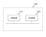
- the control device 140 includes a processing device (processor) 141 and a storage device (memory) 142.
- the processing device 141 is, for example, a CPU (central processing unit), and can realize the functions of the control device 140 by reading and executing a program stored in the storage device 142.
- the processing device 141 may be an ASIC (application-specific integrated circuit), a DSP (digital signal processor), an FPGA (field programmable gate array), or the like.
- the storage device 142 may be a ROM (read only memory), a RAM (random access memory), a HDD (hard disk drive), or the like.
- Each of the drive circuits 122 to 127 may have a configuration similar to that of the example of FIG. 2.
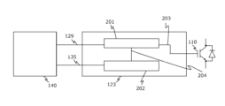
- FIG. 3 is a diagram showing an example of the configuration of the drive circuits 122 to 127 in this embodiment.
- drive circuit 123 is given as an example, and drive circuits 122, 124 to 127 have the same configuration as drive circuit 123.
- drive circuit 123 is connected to semiconductor switching element 110, the relationship between drive circuit 123 and semiconductor switching element 110 will be described as an example of the relationship between drive circuits 122 to 127 and semiconductor switching elements 109 to 114.
- the drive circuit 123 includes a drive signal conversion circuit 201 and a drive capacity adjustment circuit 202.
- the drive signal conversion circuit 201 is connected to the control device 140 by a drive control signal line 129, and a drive control signal is provided from the control device 140 to the drive signal conversion circuit 201 via the drive control signal line 129.
- the drive signal conversion circuit 201 is also connected to the control terminal of the semiconductor switching element 110 by a drive signal line 203, and a drive signal is provided from the drive signal conversion circuit 201 to the semiconductor switching element 110.
- the drive capacity adjustment circuit 202 is connected to the control device 140 by an adjustment control signal line 135, and an adjustment control signal is provided from the control device 140 to the drive capacity adjustment circuit 202 via the adjustment control signal line 135.
- the drive capacity adjustment circuit 202 is connected to the drive signal conversion circuit 201 by an adjustment signal line 204, and an adjustment signal is provided from the drive capacity adjustment circuit 202 to the drive signal conversion circuit 201 via the adjustment signal line 204. If the control device 140 cannot directly supply the voltage or power required for driving, a buffer circuit may be added between the control device 140 and the drive circuits 122 to 127.
- the drive signal conversion circuit 201 drives the semiconductor switching element 110 by providing the semiconductor switching element 110 (target semiconductor switching element) with a drive signal for turning on and off the semiconductor switching element 110.
- the drive signal conversion circuit 201 is an example of a first circuit.
- the drive capacity adjustment circuit 202 adjusts the switching speed of the semiconductor switching element 110. Specifically, the drive capacity adjustment circuit 202 outputs an adjustment signal for changing the switching speed of the semiconductor switching element 110 (target semiconductor switching element) to the drive signal conversion circuit 201.
- the drive capacity adjustment circuit 202 is an example of a second circuit.
- the drive signal conversion circuit 201 generates a drive signal based on a drive control signal provided by the control device 140. For example, when turning on the semiconductor switching element 110, the control device 140 outputs a voltage of +5V as the drive control signal, and when turning off the semiconductor switching element 110, the control device 140 outputs a voltage of 0V as the drive control signal. When a voltage signal of +5V is input to the drive signal conversion circuit 201, it outputs a voltage of +15V as the drive signal, and when a voltage of 0V is input, it outputs a voltage of 0V as the drive signal.
- the semiconductor switching element 110 turns on when a voltage of +15V is input to the control electrode, and turns off when a voltage of 0V is input. This controls the switching of the semiconductor switching element 110.
- the drive capability adjustment circuit 202 generates an adjustment signal based on the adjustment control signal provided by the control device 140, and provides the generated adjustment signal to the drive signal conversion circuit 201.
- the drive signal conversion circuit 201 generates a drive signal based on the drive control signal provided by the control device 140 as well as the adjustment signal provided by the drive capacity adjustment circuit 202. For example, the drive signal conversion circuit 201 generates a drive signal as described above based on the drive control signal from the control device 140, and then corrects the drive signal based on the adjustment signal from the drive capacity adjustment circuit 202. The drive signal conversion circuit 201 can change the switching speed of the semiconductor switching element 110 by providing the semiconductor switching element 110 with the corrected drive signal.
- a finite amount of time is required for the semiconductor switching element 110 to turn on or off after the drive signal given to the semiconductor switching element 110 changes between a voltage corresponding to on and a voltage corresponding to off.
- the time required for the semiconductor switching element 110 to switch from off to on after the drive signal changes from 0V to +15V is several tens of nanoseconds to several microseconds.
- the time required for the semiconductor switching element 110 to perform switching differs depending on the drive capacity of the drive circuit 123.
- the rate of change of the voltage between the positive and negative electrodes of the semiconductor switching element 110 (hereinafter referred to as the element voltage) and the current flowing between the positive and negative electrodes (hereinafter referred to as the element current) when the semiconductor switching element 110 is switched differs depending on the drive capacity of the drive circuit 123.
- the drive circuit 123 is configured to be able to change the drive capacity that switches the semiconductor switching element 110, and by changing the drive capacity, the switching speed of the semiconductor switching element 110 is changed.
- the drive capacity adjustment circuit 202 adjusts the drive capacity of the drive circuit 123, thereby making it possible to adjust the rate of change of the element voltage and element current when the semiconductor switching element 110 is switched.
- the switching speed of the semiconductor switching element 110 can be adjusted by adjusting the rate of change of the element voltage and element current when the semiconductor switching element 110 is switched. In other words, the rate of change of the element voltage and element current when the semiconductor switching element 110 is switched corresponds to the switching speed.
- Figure 4 is a diagram showing an example of the switching waveform of the semiconductor switching element 109 when the drive capacity of the drive circuit 122 is high.
- Figure 5 is a diagram showing an example of the switching waveform of the semiconductor switching element 109 when the drive capacity of the drive circuit 122 is low.
- the horizontal axis indicates time and the vertical axis indicates current or voltage.
- Figures 4 and 5 show voltage waveforms 301 and 401 that represent the change in element voltage when the semiconductor switching element 109 is turned off, and current waveforms 302 and 402 that represent the change in element current.
- the semiconductor switching element 109 is maintained on until time t1. Therefore, the element voltage is maintained at approximately zero. From time t1, the semiconductor switching element 109 starts to turn off, and the element voltage rises. The amount of this rise depends on the slope (di/dt) of the element current 402. The element voltage peaks at time t2, then drops slightly, and becomes constant from time t3. This completes the turn-off of the semiconductor switching element 109.
- the element current is maintained constant until time t4 after time t1, decreases in the period from time t4 to time t5, and is maintained at approximately zero from time t5.
- the semiconductor switching element 109 is maintained on until time t11. Therefore, the element voltage is maintained at approximately zero. From time t11, the semiconductor switching element 109 starts to turn off, and the element voltage rises. The element voltage reaches a peak at time t12, then drops slightly, and becomes constant from time t13. This completes the turn-off of the semiconductor switching element 109. The element current is maintained constant until time t14 after time t11, decreases in the period from time t14 to time t15, and is maintained at approximately zero from time t15.
- the relationship between the drive capacity of the drive circuits 123-127 and the rate of change of the element voltage and element current of the semiconductor switching elements 110-114 is also the same as in the examples of Figures 4 and 5. Furthermore, when the semiconductor switching elements 109-114 are turned on, the element voltage and element current change in the same manner as in the examples of Figures 4 and 5, except that the direction of change of the element voltage and element current is reversed from that in the examples of Figures 4 and 5, and recovery currents flow through the diodes connected in antiparallel.
- the element voltage rise time the length of the period from when the element voltage starts to rise until it becomes constant (the period from time t1 to time t3 in Figure 4) is referred to as the element voltage rise time.
- the semiconductor switching elements 110 to 114 are turned on, the length of the period from when the element voltage starts to fall until it becomes constant is referred to as the element voltage fall time.
- the semiconductor switching elements 110 to 114 are turned off, the length of the period from when the element current starts to fall until it becomes constant (the period from time t4 to time t5 in Figure 4) is referred to as the element current fall time.
- the semiconductor switching elements 110 to 114 are turned on, the length of the period from when the element voltage starts to rise until it becomes constant is referred to as the element current rise time.
- the rise time of the element voltage when the driving capability of the drive circuit 122 is high is shorter than the rise time of the element voltage when the driving capability of the drive circuit 122 is low. Also, the fall time of the element current when the driving capability of the drive circuit 122 is high is shorter than the fall time of the element current when the driving capability of the drive circuit 122 is low.
- the semiconductor switching elements 109-114 when the semiconductor switching elements 109-114 are turned off, the higher the driving capability of the drive circuits 122-127, the shorter the rise time of the element voltage and the fall time of the element current. This tendency is also observed when the semiconductor switching elements 109-114 are turned on. Specifically, when the semiconductor switching elements 109-114 are turned on, the higher the driving capability of the drive circuits 122-127, the shorter the fall time of the element voltage and the rise time of the element current. In other words, the higher the driving capability of the drive circuits 122-127, the faster the rate of change of the element voltage and element current.
- the switching speed of the semiconductor switching elements 109-114 corresponds to the rate of change of the element voltage and element current when the semiconductor switching elements 109-114 are switched (when turned on and off). Therefore, the higher the driving capability of the driving circuits 122-127, the higher the switching speed of the semiconductor switching elements 109-114.
- the switching speed is determined by the relationship between the rate of change of the element current and the rate of change of the element voltage. For example, if only one of the rate of change of the element current and the rate of change of the element voltage is different, the switching speed is determined by the rate of change of the other. Specifically, if the fall times of the element currents are the same at the time of turn-off, the shorter the rise time of the element voltage, the higher the switching speed. Also, if the fall times of the element voltages are the same at the time of turn-on, the shorter the rise time of the element current, the higher the switching speed.
- a first state in which the rate of change of the element current is a first rate and the rate of change of the element voltage is a second rate is compared with a second state in which the rate of change of the element current is a third rate lower than the first rate and the rate of change of the element voltage is a fourth rate higher than the second rate.
- the switching speed of the first state is higher than the switching speed of the second state.
- the difference between the second speed and the fourth speed is more dominant than the difference between the first speed and the third speed, the switching speed of the first state is lower than the switching speed of the second state.
- the losses and noise generated in the motor 115 depend on the switching speed of the semiconductor switching elements 109 to 114.
- Harmonic components are frequency components that are integer multiples of a certain fundamental wave.
- Figure 6 is a diagram that shows a schematic diagram of the relationship between a trapezoidal pulse wave and a frequency spectrum.
- the horizontal axis indicates frequency
- the vertical axis indicates gain. It is assumed that the pulse wave rises and falls linearly.
- the tendency of the gain change differs depending on the frequency band. Specifically, in frequency bands below F1, the gain is constant. In frequency bands from F1 to F2, the gain attenuates with a first slope 501 as the frequency increases. In frequency bands above F2, the gain attenuates with a second slope 502 as the frequency increases. The second slope 502 is greater than the first slope 501.
- a larger slope means a larger degree of change.
- the frequency band in which the gain is constant (below F1 in the example of FIG. 6) is referred to as the first frequency band
- the frequency band in which the gain attenuates with the first slope 501 from F1 to F2 in the example of FIG. 6)
- the frequency band in which the gain attenuates with the second slope 502 is referred to as the third frequency band (F2 or more in the example of FIG. 6).
- the frequency that is the boundary between the first and second frequency bands depends on the pulse width of the pulse wave.
- the larger the pulse width the lower the first boundary frequency.
- the larger the pulse width the lower the frequency of the pulse wave.
- the lower the frequency of the pulse wave the lower the first boundary frequency.
- the second boundary frequency the second boundary frequency
- the frequency that is the boundary between the second and third frequency bands depends on the rise time and fall time of the pulse wave. The longer the rise time and fall time, the lower the second boundary frequency.
- the lower the frequency of the pulse wave the smaller the gain of the harmonic components.
- the longer the rise time and fall time of the pulse wave the smaller the gain of the harmonic components.
- the smaller the gain of the harmonic components the smaller the harmonic components of the noise. Therefore, the lower the frequency of the pulse wave, the less noise there is. Also, the longer the rise time and fall time of the pulse wave, the less noise there is.
- the switching speed of the semiconductor switching elements 109-114 corresponds to the rise time and fall time of the pulse wave, and a long rise time and fall time corresponds to a low switching speed. Therefore, by lowering the switching speed of the semiconductor switching elements 109-114 by lowering the driving capacity of the driving circuits 122-127, the content of harmonic components is reduced, and the overall amount of noise generated can be reduced.
- the heat pump device 100 has two operation modes: a normal operation mode and a heating operation mode. There are various detailed control methods for the normal operation mode and the heating operation mode, but detailed explanations of the control contents will be omitted in this disclosure.
- the inverter 160 rotates the motor 115, which drives the compression mechanism 116.
- the refrigerant is compressed by the compression mechanism 116, and the compressed refrigerant is used for heat exchange in the heat pump device 100.
- the frequency of the current flowing through the motor 115 is on the order of several Hz to several tens of Hz.
- the switching frequency of the semiconductor switching elements 109 to 114 of the inverter 160 is on the order of several kHz.
- the switching frequency in normal operation mode is 5 kHz.
- the switching frequency of the semiconductor switching elements 109 to 114 is higher than the frequency of the current flowing through the motor 115.
- the driving capacity of the drive circuits 122-127 may be set to the lowest condition depending on the operating conditions of the heat pump device 100. For example, when the current of the inverter 160, which has low losses to begin with, is small, or when the current is high and there is concern that noise may increase, the driving capacity of the drive circuits 122-127 may be maintained at the lowest condition. However, since the driving capacity of the drive circuits 122-127 will decrease, it is preferable to check in advance whether the loss is within an acceptable range.
- the heating operation mode is an operation mode in which the inverter 160 passes a high-frequency current through the motor 115 that does not rotate the motor 115, causing the motor 115 to generate loss (heat) without driving the compression mechanism 116.
- the high-frequency current here refers to a current with a frequency that does not generate rotational torque in the motor 115, for example, a current with a frequency of several kHz to several tens of kHz or more.
- the loss generated by the motor 115 makes it possible to heat the refrigerant in the compressor 117.
- the loss generated by the motor 115 includes, for example, iron loss caused by electromagnetic induction heating due to the high-frequency current, and copper loss generated by the flow of current.
- the heating operation mode can improve stagnation.
- Stagnation is a phenomenon in which refrigerant gas liquefies and returns to compressor 117 during operation shutdowns when the ambient temperature drops, such as in winter, causing the refrigerant to stagnate within the compressor. If the amount of stagnation increases, the lubricating oil inside compressor 117 may be diluted by the refrigerant. If the degree of dilution is severe, the viscosity of the lubricating oil may decrease, causing it to not function adequately as a lubricating oil, or the compressor 117 may break down. For this reason, stagnation can be prevented by using the heating operation mode to heat and gasify the refrigerant stagnate within compressor 117.
- FIG. 7 is a flowchart showing an overview of the operation of the control device 140. The operation in FIG. 7 is initiated, for example, by starting up the heat pump device 100 and is terminated by stopping the operation of the heat pump device 100.
- step S1 the control device 140 selects an operation mode for the heat pump device 100. For example, the control device 140 determines whether a predetermined time has passed since the heat pump device 100 was started. If the predetermined time has not passed since the heat pump device 100 was started, the refrigerant stagnation may not have been sufficiently improved, so the control device 140 selects the heating operation mode. If a predetermined time has passed since the heat pump device 100 was started, the control device 140 selects the normal operation mode. The predetermined time is set to a time that will improve the refrigerant stagnation to a predetermined state by operation in the heating operation mode. Alternatively, the operation mode may be specified by the user, and the control device 140 may select the specified operation mode.
- the control device 140 may select the operation mode based on the state of the refrigerant in the compressor 117.
- a refrigeration detector is provided that detects the degree of refrigerant stagnation in the compressor 117.
- the degree of stagnation is represented, for example, by the amount of liquefied refrigerant remaining or the concentration of lubricating oil.
- the control device 140 determines whether or not the refrigerant needs to be heated based on the detection result of the stagnation detector. If the refrigerant needs to be heated, the control device 140 selects the heating operation mode, and if the refrigerant does not need to be heated, the control device 140 selects the normal operation mode.
- the operation mode may be selected based on the state of the refrigerant in the compressor 117 when the operation of the heat pump device 100 is stopped. For example, if there is a possibility that refrigerant stagnation is occurring, the heating operation mode may be selected.
- step S2 the control device 140 determines the switching frequency and switching speed of the semiconductor switching elements 109-114 based on the selected operation mode.
- the control device 140 determines the switching frequency of the semiconductor switching elements 109-114 so that the switching frequency of the semiconductor switching elements 109-114 in the heating operation mode is higher than the switching frequency of the semiconductor switching elements 109-114 in the normal operation mode.
- the control device 140 also determines the switching speed of the semiconductor switching elements 109-114 so that the switching speed of the semiconductor switching elements 109-114 in the heating operation mode is lower than the switching speed of the semiconductor switching elements 109-114 in the normal operation mode.
- step S3 the control device 140 generates a drive control signal and an adjustment control signal so that the semiconductor switching elements 109-114 are driven at the determined switching frequency and switching speed.
- step S4 the control device 140 provides the generated drive control signal and adjustment control signal to the drive circuits 122-127.
- the drive circuits 122-127 generate drive signals based on the drive control signal and adjustment control signal from the control device 140, and provide the generated drive signals to the semiconductor switching elements 109-114. This drives the semiconductor switching elements 109-114.
- the control device 140 then repeats the processing of steps S1-S4.
- the semiconductor switching elements 109 to 114 are driven so that the switching speed of the semiconductor switching elements 109 to 114 in the heating operation mode is lower than the switching speed of the semiconductor switching elements 109 to 114 in the normal operation mode. This makes it possible to suppress an increase in noise in the heating operation mode. The details are described below.
- the switching frequency refers to the switching frequency of the semiconductor switching elements 109 to 114
- the switching speed refers to the switching speed of the semiconductor switching elements 109 to 114
- the motor current frequency refers to the frequency of the current flowing through the motor 115.
- the motor current frequency in the heating operation mode is higher than the motor current frequency in the normal operation mode, for example, several kHz to several tens of kHz.
- the switching frequency in the heating operation mode may be equal to the motor current frequency in the heating operation mode.
- the heating operation mode has the following effects:
- the frequency of the vibration sound of the motor 115 increases to a frequency outside the audible range, which has the effect of reducing noise.
- the frequency of the vibration sound of the iron core of the motor 115 is generally outside the audible range, reducing noise.
- the power used in the normal operation mode is large, such as several kilowatts or tens of kilowatts
- the power used in the heating operation mode is only several tens of watts, which is smaller than the power used in the normal operation mode.
- the current flowing through the semiconductor switching elements 109-114 in the heating operation mode is smaller than the current flowing through the semiconductor switching elements 109-114 in the normal operation mode. Therefore, the loss generated in the semiconductor switching elements 109-114 in the heating operation mode is smaller than the loss generated in the semiconductor switching elements 109-114 in the normal operation mode.
- the switching frequency in the heating operation mode is higher than the switching frequency in the normal operation mode.
- the switching frequency in the heating operation mode is higher than the switching frequency in the normal operation mode, there is a concern that noise will increase in the heating operation mode.
- Noise includes, for example, conductive noise that is transmitted through conductors such as power and signal cables and thin-film wiring on printed circuit boards, and radiated noise that is emitted into space.
- Radio frequency interference is generated from household electrical appliances, power tools, and similar devices whose main functions are performed by motors 115 and switches or control elements.
- CISPL14 a standard that applies to the conduction and radiation of radio frequency interference, specifies noise requirements of 150 kHz to 30 MHz for conducted noise and 30 MHz to 1 GHz for radiated noise. As described above, if the switching frequency in the heating operation mode is several kHz to several tens of kHz, the switching frequency in the heating operation mode falls outside the frequency band of the standard.
- the switching frequency may be within the frequency band of the above standard. This is because the next-generation semiconductor materials have the properties of low loss and high switching speed, which means that the semiconductor switching elements 109-114 generate less heat and the switching frequency can be increased. As a result, by using next-generation semiconductor materials, the switching frequency may be 150 kHz or higher. A switching frequency of 150 kHz or higher is within the frequency band of the above standard.
- harmonic noise having a frequency that is an integer multiple of the switching frequency may occur, and this harmonic noise may exceed the standard value within the frequency range of the above standard.
- harmonic noise may easily pass through in the resonant frequency band due to the inductance or capacitance components on the circuit, including parasitic components, and may exceed the standard value within the frequency range of the above standard.
- harmonic noise generated by the switching of the semiconductor switching elements 109 to 114 can become interference waves for other devices. Therefore, it is necessary to suppress the increase in noise.
- the content of harmonic components varies depending on the switching speed of the semiconductor switching elements 109 to 114. Therefore, in this embodiment, by adjusting the driving capabilities of the drive circuits 122 to 127, it is possible to change the switching speed of the semiconductor switching elements 109 to 114 and reduce the content of harmonic components that become noise.
- the drive circuits 122-127 drive the multiple semiconductor switching elements 109-114 so that the switching speed in the heating operation mode is lower than the switching speed in the normal operation mode.
- the switching speed is lower than in the normal operation mode, so that harmonic components can be reduced and an increase in noise can be suppressed.
- the drive circuits 122-127 are configured to be able to adjust the switching speed of the semiconductor switching elements 109-114 (target semiconductor switching elements) at turn-on and at turn-off in an integrated manner.
- a common adjustment control signal for turn-on and turn-off is provided from the control device 140 to the drive capacity adjustment circuits 202 of the drive circuits 122-127.
- Each drive capacity adjustment circuit 202 adjusts the switching speed at turn-on and the switching speed at turn-off, respectively, based on the common adjustment control signal from the control device 140.
- the drive capacity adjustment circuit 202 adjusts the switching speed at turn-on and the switching speed at turn-off to be relatively low, respectively, and when a voltage signal of +5V is provided as the adjustment control signal, the drive capacity adjustment circuit 202 adjusts the switching speed at turn-on and the switching speed at turn-off to be relatively high, respectively.
- a common adjustment control signal means an adjustment control signal that corresponds to a common condition. For example, if the adjustment control signal is a voltage signal, an adjustment control signal of a common voltage value corresponds to a common adjustment control signal, and an adjustment control signal of a different voltage value does not correspond to a common adjustment control signal. Specifically, an adjustment control signal of 0V and an adjustment control signal of 5V do not correspond to a common adjustment control signal.
- the switching speed at turn-on and the switching speed at turn-off may be the same as each other or may be different from each other.
- the precision of the switching speed adjustment varies depending on the circuit configuration or the method of adjusting the switching speed. Therefore, even if the switching speed at turn-on and the switching speed at turn-off are adjusted based on a common adjustment control signal, they do not necessarily match each other.
- the drive circuits 122-127 may be configured to be able to individually adjust the switching speed of the semiconductor switching elements 109-114 (target semiconductor switching elements) when turned on and the switching speed of the semiconductor switching elements 109-114 (target semiconductor switching elements) when turned off.
- the control device 140 provides individual adjustment control signals for turn-on and turn-off to the drive capacity adjustment circuits 202 of the drive circuits 122-127.
- Each drive capacity adjustment circuit 202 adjusts the switching speed when turned on based on the turn-on adjustment control signal from the control device 140, and adjusts the switching speed when turned off based on the turn-off adjustment control signal from the control device 140.
- the drive capacity adjustment circuit 202 adjusts the switching speed when turned on to be relatively low and adjusts the switching speed when turned off to be relatively high. This allows the switching speed when turned on and the switching speed when turned off to be individually adjusted.
- the switching speed at turn-on and the switching speed at turn-off separately, more fine adjustments can be made that take losses and noise into account. For example, if the noise generated at one of turn-on and turn-off is greater than the noise generated at the other, the switching speed may be adjusted so that the switching speed at one is slower than the switching speed at the other.
- the turn-on adjustment control signal and the turn-off adjustment control signal may be provided to each drive capacity adjustment circuit 202 via a common adjustment control signal line, or may be provided to each drive capacity adjustment circuit 202 via different adjustment control signal lines.
- the turn-on adjustment control signal and the turn-off adjustment control signal are provided to each drive capacity adjustment circuit 202 via a common adjustment control signal line, for example, the turn-on adjustment control signal and the turn-off adjustment control signal are provided alternately at a constant period. For example, a voltage signal of 0V and a voltage signal of +5V are provided alternately.
- the drive capacity adjustment circuit 202 adjusts the switching speed at turn-on based on the turn-on adjustment control signal, and adjusts the switching speed at turn-off based on the turn-off adjustment control signal.
- the switching speed at turn-on and the switching speed at turn-off can be adjusted individually while suppressing an increase in the adjustment control signal line.
- each drive capacity adjustment circuit 202 When the turn-on adjustment control signal and the turn-off adjustment control signal are provided to each drive capacity adjustment circuit 202 via different adjustment control signal lines, two adjustment control signal lines 134 to 139 in FIG. 1 are provided for each. A turn-on adjustment control signal is provided via one adjustment control signal line, and a turn-off adjustment control signal is provided via the other adjustment control signal line.
- the drive capacity adjustment circuit 202 adjusts the switching speed at turn-on based on the adjustment control signal provided via one adjustment control signal line, and adjusts the switching speed at turn-off based on the adjustment control signal provided via the other adjustment control signal line. In this case, since there is no need to distinguish between the turn-on adjustment control signal and the turn-off adjustment control signal, the configuration of the drive capacity adjustment circuit 202 is prevented from becoming complicated.
- the switching speed at turn-on may be selectable from three or more multiple speeds
- the switching speed at turn-off may be selectable from three or more multiple speeds. Increasing the number of selectable speeds allows for more fine adjustments, and the increase in noise can be more effectively suppressed.
- the voltage signal as the adjustment control signal is set in the range of 0V to +5V so that 0V corresponds to the lowest switching speed (driving capacity) and +5V corresponds to the highest switching speed (driving capacity).
- the control device 140 provides the drive capacity adjustment circuit 202 with an adjustment control signal of 0V
- the drive circuit 122 adjusts the switching speed to the lowest speed.
- the control device 140 provides the drive capacity adjustment circuit 202 with an adjustment control signal of +5V
- the drive circuit 122 adjusts the switching speed to the highest speed.
- the drive circuit 122 adjusts the switching speed to an intermediate speed between the lowest speed and the highest speed.
- the intermediate speed may be set in multiple stages.
- the voltage range is an example, and can be set to any voltage range, such as 0V to +15V, -5V to +5V, or +5V to +15V.
- a voltage generated by a voltage conversion device such as rectifier 150 or inverter 160 may be used as the voltage of the voltage signal.
- the switching speed may be switchable only between two switching speeds: the switching speed for the normal operation mode and the switching speed for the heating operation mode. In this case, it is possible to simplify the drive circuits 122 to 127 and the control device 140.
- the drive circuits 122-127 maintain a constant drive capacity during the heating operation mode, for example. This makes it possible to suppress an increase in noise without performing complex control.
- the drive capacity of the drive circuits 122-127 may be changed by providing an adjustment control signal from the control device 140 to the drive circuits 122-127 before the heating operation mode is started, or the drive capacity of the drive circuits 122-127 may be switched by inputting an adjustment control signal from the control device 140 to the drive circuits 122-127 after the heating operation mode is started.
- the drive circuits 122-127 may change their drive capabilities during the heating operation mode. For example, the adjustment signal provided to the drive circuits 122-127 by the control device 140 is changed based on the current flowing through the motor 115 or the voltage applied to the motor 115 during the heating operation mode, thereby changing the drive capabilities of the semiconductor switching elements 109-114.
- the drive capabilities of the drive circuits 122-127 in response to changes in the current flowing through the motor 115 or the voltage applied to the motor 115 during the heating operation mode, an increase in noise can be appropriately suppressed.
- Figure 8 is a diagram that shows a schematic diagram of the relationship between the operating mode and the frequency spectrum. Like Figure 6, Figure 8 shows the frequency spectrum of a trapezoidal pulse wave. Also, like Figure 6, the horizontal axis shows the frequency, and the vertical axis shows the gain. It is assumed that the pulse wave rises and falls linearly.
- the solid line 601 shows the frequency spectrum (hereinafter referred to as the first frequency spectrum) when the frequency is 5 kHz and the rise and fall times are each 50 ns (hereinafter referred to as the first condition).
- the frequency of the first condition corresponds to the switching frequency in the normal operation mode, and the solid line 601 simply represents the frequency spectrum in the normal operation mode.
- the dotted line 602 shows the frequency spectrum (hereinafter referred to as the second frequency spectrum) when the frequency is 20 kHz and the rise and fall times are each 50 ns (hereinafter referred to as the second condition).
- the dashed and dotted line 603 shows the frequency spectrum (hereinafter referred to as the third frequency spectrum) when the frequency is 20 kHz and the rise and fall times are each 200 ns (hereinafter referred to as the third condition).
- the frequencies of the second and third conditions correspond to the switching frequency in the heating operation mode, and the dotted line 602 and the dashed-dotted line 603 simply represent the frequency spectrum in the heating operation mode.
- the rise time and fall time of the third condition are longer than the rise time and fall time of the second condition, respectively.
- each of the first to third frequency spectra has a different tendency depending on the frequency band.
- the gain is constant in the first frequency band
- the gain attenuates with a first slope in the second frequency band
- the gain attenuates with a second slope in the third frequency band.
- the first boundary frequency that is the boundary between the first and second frequency bands depends on the frequency of the pulse wave
- the second boundary frequency that is the boundary between the second and third frequency bands depends on the rise time and fall time of the pulse wave.
- the first frequency spectrum (solid line 601) is compared with the second frequency spectrum (dotted line 602). Because the frequency under the second condition is higher than the frequency under the first condition, the first boundary frequency of the second frequency spectrum is higher than the first boundary frequency of the first frequency spectrum. Also, because the rise time and fall time under the first condition are the same as the rise time and fall time under the second condition, respectively, the second boundary frequency of the first frequency spectrum is the same as the second boundary frequency of the first frequency spectrum.
- the gain of the second frequency spectrum is greater than the gain of the first frequency spectrum in a frequency band higher than the first boundary frequency of the first frequency spectrum.
- the content of harmonic components in the second frequency spectrum is greater than the content of harmonic components in the first frequency spectrum.
- the switching speed corresponds to the rise time and fall time of the pulse wave.
- a comparison of the first frequency spectrum (solid line 601) and the second frequency spectrum (dotted line 602) shows that when the switching speed remains the same and the switching frequency increases, the amount of noise generated increases.
- the second frequency spectrum (dotted line 602) is compared with the third frequency spectrum (dashed-dotted line 603). Because the frequency of the second condition is the same as the frequency of the third condition, the first boundary frequency of the second frequency spectrum is the same as the second boundary frequency of the third frequency spectrum. Also, because the rise time and fall time of the third condition are longer than the rise time and fall time of the second condition, the second boundary frequency of the third frequency spectrum is lower than the second boundary frequency of the second frequency spectrum.
- the heat pump device 100 of this embodiment is a heat pump device having a normal operation mode and a heating operation mode, and includes a compression mechanism 116 that compresses a refrigerant, a motor 115 that drives the compression mechanism 116, semiconductor switching elements 109-114, an inverter 160 that applies a voltage to the motor 115, and drive circuits 122-127 that drive the semiconductor switching elements 109-114
- the normal operation mode is an operation mode in which the motor 115 drives the compression mechanism 116
- the heating operation mode is an operation mode in which the motor 115 heats the refrigerant by generating losses without driving the compression mechanism 116
- the semiconductor switching elements 109-114 include at least one target semiconductor switching element
- the drive circuits 122-127 drive the semiconductor switching elements 109-114 so that the switching speed of the target semiconductor switching element in the heating operation mode is lower than the switching speed of the target semiconductor switching element in the normal operation mode.
- each of the semiconductor switching elements 109 to 114 is a
- the switching frequency becomes high in order to pass a high-frequency current through the motor 115. If the switching speed in the heating operation mode is the same as the switching speed in the normal operation mode, the high-frequency components that become noise will increase. However, in the heat pump device 100 of this embodiment, the switching speed of the semiconductor switching elements 109-114 in the heating operation mode is lower than the switching speed of the semiconductor switching elements 109-114 in the normal operation mode, so that the high-frequency components are reduced. As a result, it is possible to suppress an increase in noise when the refrigerant is heated.
- each of the semiconductor switching elements 109 to 114 is a target semiconductor switching element, but only some of the semiconductor switching elements 109 to 114 may be target semiconductor switching elements. In that case, the switching speed of only the target semiconductor switching elements among the semiconductor switching elements 109 to 114 is adjusted according to the operation mode, and the switching speed of the other semiconductor switching elements is constant regardless of the operation mode.
- the switching speed of the target semiconductor switching element in the heating operation mode is always adjusted to be lower than the switching speed of the target semiconductor switching element in the normal operation mode, but due to the effects of noise and other conditions, the switching speed of the target semiconductor switching element in the heating operation mode may temporarily become higher than the switching speed of the target semiconductor switching element in the normal operation mode.
- the power system 101 is assumed to be a three-phase, three-wire AC system, and is therefore connected to three wires, namely, connection point a, connection point b, and connection point c; however, the power system 101 may be a single-phase AC system. If the power system 101 is a single-phase AC system, the power system 101 is connected to two wires. For example, the rectifier 150 does not include diodes 106 and 107, and the power system 101 is not connected to connection point c.
- the power system 101 may also be a three-phase, four-wire AC system, in which case a ground wire is added to the heat pump device 100.
- the rectifier 150 is composed only of the diodes 102 to 107, but the configuration of the rectifier 150 is not limited to this.
- the rectifier 150 may have a configuration in which a semiconductor switching element is connected in parallel with each of the diodes 102 to 107, and the switching operation of the semiconductor switching element is possible.
- a boost chopper circuit may be connected between the rectifier 150 and the smoothing capacitor 108.
- the voltage applied to the smoothing capacitor 108 can be set by the boost chopper circuit to be higher than the AC voltage from the power system 101. This allows a higher voltage to be applied to the motor 115, thereby increasing the output of the motor 115.
- the boost chopper circuit as a high power factor converter that brings the current from the power system 101 closer to a sine wave, harmonic distortion of the current flowing in from the AC system can be reduced.
- the drive signal conversion circuit 201 and the drive capacity adjustment circuit 202 are provided separately, but the drive signal conversion circuit 201 may have the function of the drive capacity adjustment circuit 202.
- the control device 140 may be connected to the drive signal conversion circuit 201 by the drive control signal line 128 and the adjustment control signal line 134, and both the drive control signal and the adjustment control signal may be provided from the control device 140 to the drive signal conversion circuit 201.
- the adjustment control signal is generated by the control device 140, but a circuit for generating the adjustment control signal may be provided separately from the control device 140.
- the circuit for generating the adjustment control signal may be connected to the drive capacity adjustment circuit 202, and the circuit for generating the adjustment control signal may provide the adjustment control signal to the drive capacity adjustment circuit 202.
- the control device 140 may also adjust the switching speed of the semiconductor switching elements 109 to 114 by providing a digital signal as an adjustment control signal to the drive capacity adjustment circuit 202 of the drive circuits 122 to 127.
- the drive capacity adjustment circuit 202 has a function of decoding a digital signal, and by decoding the digital signal provided as the adjustment control signal, it is possible to finely adjust the drive capacity of the drive circuits 122 to 127. It is possible to adjust the drive capacity of the drive circuits 122 to 127 whether an analog signal (for example, a voltage signal) is used or a digital signal is used.
- a voltage of 0V may be used as a signal of 0 and a voltage of +5V as a signal of 1. In this case, it is possible to adjust the drive capacity with a simple configuration.
- any method can be used as long as it can change the switching speed of the semiconductor switching elements 109-114.
- the control device 140 individually provides adjustment control signals to the drive circuits 122 to 127.
- the control devices 122 to 127 individually provide adjustment control signals, it becomes possible to individually adjust the operation of the semiconductor switching elements 109 to 114.
- the control device 140 may provide the same adjustment control signal to the drive circuits 122 to 127.
- FIG. 9 is a diagram showing a configuration example of a modified example of the heat pump device 100 according to the embodiment. As shown in FIG. 9, the control device 140 provides the same adjustment control signal to the drive circuits 122 to 127. In this case, the switching speeds of the semiconductor switching elements 109 to 114 are commonly adjusted. When the semiconductor switching elements 109 to 114 are operated with the same drive capacity, the control of the inverter 160 is simplified because the adjustment control signal output from the control device 140 can be common.
- 100 heat pump device 101 power system, 102, 103, 104, 105, 106, 107 diode, 108 smoothing capacitor, 109, 110, 111, 112, 113, 114 semiconductor switching element, 115 motor, 116 compression mechanism, 117 compressor, 122, 123, 124, 125, 126, 127 drive circuit, 128, 129, 130, 131, 132, 133 drive control signal line, 134, 135, 136, 137, 138, 139 adjustment control signal line, 140 control device, 141 processing device, 142 storage device, 150 rectifier, 160 inverter, 201 drive signal conversion circuit, 202 drive capacity adjustment circuit, 203 drive signal line, 204 adjustment signal line, 301, 401 voltage waveform, 302, 402 current waveform, 501 first slope, 502 second slope, 601 solid line, 602 dotted line, 603 dashed line, S1, S2, S3, S4 steps, a, b, c, d, e, f, g,
Landscapes
- Engineering & Computer Science (AREA)
- Physics & Mathematics (AREA)
- Mechanical Engineering (AREA)
- Thermal Sciences (AREA)
- General Engineering & Computer Science (AREA)
- Power Conversion In General (AREA)
Priority Applications (2)
| Application Number | Priority Date | Filing Date | Title |
|---|---|---|---|
| PCT/JP2023/037965 WO2025083865A1 (ja) | 2023-10-20 | 2023-10-20 | ヒートポンプ装置および駆動回路 |
| JP2025533534A JPWO2025083865A1 (https=) | 2023-10-20 | 2023-10-20 |
Applications Claiming Priority (1)
| Application Number | Priority Date | Filing Date | Title |
|---|---|---|---|
| PCT/JP2023/037965 WO2025083865A1 (ja) | 2023-10-20 | 2023-10-20 | ヒートポンプ装置および駆動回路 |
Publications (1)
| Publication Number | Publication Date |
|---|---|
| WO2025083865A1 true WO2025083865A1 (ja) | 2025-04-24 |
Family
ID=95448742
Family Applications (1)
| Application Number | Title | Priority Date | Filing Date |
|---|---|---|---|
| PCT/JP2023/037965 Pending WO2025083865A1 (ja) | 2023-10-20 | 2023-10-20 | ヒートポンプ装置および駆動回路 |
Country Status (2)
| Country | Link |
|---|---|
| JP (1) | JPWO2025083865A1 (https=) |
| WO (1) | WO2025083865A1 (https=) |
Citations (3)
| Publication number | Priority date | Publication date | Assignee | Title |
|---|---|---|---|---|
| JP2015171226A (ja) * | 2014-03-06 | 2015-09-28 | 三菱電機株式会社 | インバータ装置及び空気調和機 |
| WO2016046993A1 (ja) * | 2014-09-26 | 2016-03-31 | 三菱電機株式会社 | ヒートポンプ装置ならびに、それを備えた空気調和機、ヒートポンプ給湯機、冷蔵庫、および冷凍機 |
| JP2023051225A (ja) * | 2021-09-30 | 2023-04-11 | 株式会社デンソー | 回転電機の制御装置及び回転電機の制御方法 |
Family Cites Families (1)
| Publication number | Priority date | Publication date | Assignee | Title |
|---|---|---|---|---|
| JP4985723B2 (ja) * | 2009-07-27 | 2012-07-25 | 三菱電機株式会社 | 空気調和機 |
-
2023
- 2023-10-20 WO PCT/JP2023/037965 patent/WO2025083865A1/ja active Pending
- 2023-10-20 JP JP2025533534A patent/JPWO2025083865A1/ja active Pending
Patent Citations (3)
| Publication number | Priority date | Publication date | Assignee | Title |
|---|---|---|---|---|
| JP2015171226A (ja) * | 2014-03-06 | 2015-09-28 | 三菱電機株式会社 | インバータ装置及び空気調和機 |
| WO2016046993A1 (ja) * | 2014-09-26 | 2016-03-31 | 三菱電機株式会社 | ヒートポンプ装置ならびに、それを備えた空気調和機、ヒートポンプ給湯機、冷蔵庫、および冷凍機 |
| JP2023051225A (ja) * | 2021-09-30 | 2023-04-11 | 株式会社デンソー | 回転電機の制御装置及び回転電機の制御方法 |
Also Published As
| Publication number | Publication date |
|---|---|
| JPWO2025083865A1 (https=) | 2025-04-24 |
Similar Documents
| Publication | Publication Date | Title |
|---|---|---|
| JP5892997B2 (ja) | コンバータ回路、並びにそれを備えたモータ駆動制御装置、空気調和機、及び冷蔵庫 | |
| JP4637169B2 (ja) | 変速駆動装置を制御するためのシステムおよび方法 | |
| JP6305546B2 (ja) | 電動機駆動装置及びこれを用いた空気調和装置あるいは冷凍空調装置 | |
| EP2031753A2 (en) | Junction temperature reduction of a power semiconductor module in a three phase inverter | |
| EP3182574B1 (en) | Converter unit, drive controller, motor, and compressor | |
| US20150155804A1 (en) | Motor driving device | |
| WO2015079504A1 (ja) | 直流電源装置、およびそれを備えた冷凍サイクル適用機器 | |
| KR102507936B1 (ko) | 전력 변환 장치, 모터 구동 장치 및 공기 조화기 | |
| JP2006042529A (ja) | 空気調和装置のインバータ制御装置 | |
| CN109155601B (zh) | 电机驱动装置和具有使用该电机驱动装置的压缩机的电设备 | |
| US11804786B2 (en) | Power converting apparatus, motor driving apparatus, and air conditioner | |
| JP2022118033A (ja) | 空気調和機 | |
| JP7045529B2 (ja) | 電力変換装置および空気調和機 | |
| JP4879330B2 (ja) | 空気調和装置のインバータ制御装置 | |
| WO2025083865A1 (ja) | ヒートポンプ装置および駆動回路 | |
| CN114287104B (zh) | 电力变换装置、马达驱动装置以及空调机 | |
| KR102022965B1 (ko) | 부하 제어 효율이 개선된 인버터 제어장치 및 방법 | |
| JPWO2020066029A1 (ja) | モータ駆動装置及び空気調和機 | |
| WO2023243003A1 (ja) | 電力変換装置、モータ駆動装置及び冷凍サイクル適用機器 | |
| JP6584689B2 (ja) | 電力変換装置、冷凍サイクル装置および空気調和機 | |
| WO2023238301A1 (ja) | 電力変換装置、モータ駆動装置及びヒートポンプ装置 | |
| WO2025013205A1 (ja) | 電力変換装置、モータ駆動装置および冷凍サイクル適用機器 | |
| WO2025083878A1 (ja) | 電力変換装置、モータ駆動装置および冷凍サイクル適用機器 | |
| WO2023238291A1 (ja) | 電力変換装置、モータ駆動装置および冷凍サイクル適用機器 | |
| WO2023238293A1 (ja) | 空気調和機 |
Legal Events
| Date | Code | Title | Description |
|---|---|---|---|
| ENP | Entry into the national phase |
Ref document number: 2025533534 Country of ref document: JP Kind code of ref document: A |
|
| WWE | Wipo information: entry into national phase |
Ref document number: 2025533534 Country of ref document: JP |
|
| 121 | Ep: the epo has been informed by wipo that ep was designated in this application |
Ref document number: 23956112 Country of ref document: EP Kind code of ref document: A1 |