WO2025079129A1 - 電子制御装置、及び、電子制御装置の製造方法 - Google Patents
電子制御装置、及び、電子制御装置の製造方法 Download PDFInfo
- Publication number
- WO2025079129A1 WO2025079129A1 PCT/JP2023/036694 JP2023036694W WO2025079129A1 WO 2025079129 A1 WO2025079129 A1 WO 2025079129A1 JP 2023036694 W JP2023036694 W JP 2023036694W WO 2025079129 A1 WO2025079129 A1 WO 2025079129A1
- Authority
- WO
- WIPO (PCT)
- Prior art keywords
- ground pattern
- conductor
- shielding material
- circuit board
- control device
- Prior art date
- Legal status (The legal status is an assumption and is not a legal conclusion. Google has not performed a legal analysis and makes no representation as to the accuracy of the status listed.)
- Pending
Links
Images








Classifications
-
- H—ELECTRICITY
- H05—ELECTRIC TECHNIQUES NOT OTHERWISE PROVIDED FOR
- H05K—PRINTED CIRCUITS; CASINGS OR CONSTRUCTIONAL DETAILS OF ELECTRIC APPARATUS; MANUFACTURE OF ASSEMBLAGES OF ELECTRICAL COMPONENTS
- H05K9/00—Screening of apparatus or components against electric or magnetic fields
Definitions
- FIG. 13 is an enlarged cross-sectional view showing the arrangement of a circuit board, a housing base, and an electromagnetic shielding material included in an electronic control device according to a seventh embodiment.
- FIG. 13 is an enlarged cross-sectional view showing the arrangement of a circuit board, a housing base, and an electromagnetic shielding material included in an electronic control device according to an eighth embodiment.
- FIG. 13 is an enlarged cross-sectional view showing the arrangement of a circuit board, a housing base, and an electromagnetic wave shielding material provided in an electronic control device according to a ninth embodiment.
- FIG. 13 is an enlarged cross-sectional view showing the arrangement of a circuit board, a housing base, and an electromagnetic wave shielding material provided in an electronic control device according to a tenth embodiment.
- FIG. 12 is an enlarged cross-sectional view showing the arrangement of a circuit board, a housing base, and an electromagnetic wave shielding material provided in an electronic control device according to an eleventh embodiment.
- FIG. 23 is an enlarged cross-sectional view showing the arrangement of a circuit board, a housing base, and an electromagnetic wave shielding material provided in an electronic control device according to a twelfth embodiment.
- FIG. 23 is an enlarged cross-sectional view showing the arrangement of a circuit board, a housing base, and an electromagnetic wave shielding material provided in an electronic control device according to a thirteenth embodiment.
- FIG. 23 is an enlarged cross-sectional view showing the arrangement of a circuit board, a housing base, and an electromagnetic wave shielding material provided in an electronic control device according to a fourteenth embodiment.
- FIG. 23 is an enlarged cross-sectional view showing the arrangement of a circuit board, a housing base, and an electromagnetic wave shielding material provided in an electronic control device according to a fourteenth embodiment.
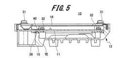
- a plurality of cover pedestals 30 are formed on the housing base 15.
- the cover pedestals 30 are formed integrally with the housing base 15.
- Each cover pedestal 30 has a screw hole 34.
- a plurality of cover fixing holes 35 are formed on the housing cover 16.
- Each cover fixing hole 35 is a through hole for fixing the housing cover 16 to the housing base 15.
- a plurality of screws 31 are engaged with the screw holes 34 of the cover pedestal 30 through the corresponding cover fixing holes 35.
- the housing cover 16 is fixed to the housing base 15 by tightening the respective screws 31. By fixing the housing cover 16 to the housing base 15 in this manner with the screws 31, the housing base 15 and the housing cover 16 are electrically and mechanically connected.
- the side on which the housing base 15 is arranged may be referred to as the lower side, and the side on which the housing cover 16 is arranged may be referred to as the upper side.
- the electronic control device 10 may be mounted in any orientation. In general, it is preferable to mount the electronic control device 10 on a vehicle so that the housing base 15 faces upward and the housing cover 16 faces downward.
- FIG. 4 is a schematic plan view of the circuit board according to the first embodiment. 4 , three electronic components 17, 18, and 19 and two connectors 21 and 22 are mounted on the circuit board 11.
- the circuit board 11 has a circuit area 25 and a ground pattern 26. Each of the electronic components 17, 18, and 19 is mounted on the circuit area 25 of the circuit board 11.
- Each of the connectors 21 and 22 is mounted on an end of the circuit board 11.
- Each of the electronic components 17, 18, 19 is an LSI element that functions as, for example, a CPU.
- LSI is an abbreviation for Large Scale Integration.
- Each of the electronic components 17, 18, 19 is a heat source and a noise source.
- the circuit area 25 of the circuit board 11 is an area in which electronic components other than the LSI elements are also mounted. In other words, the circuit area 25 is a component mounting area in which various electronic components are mounted. In FIG. 4, electronic components other than the LSI elements and wiring patterns of circuit wiring for signal transmission, power supply, etc. are omitted.
- a cable side connector (not shown) can be connected to each of the connectors 21, 22 through the opening 13 (FIG. 1) of the housing 12.
- the ground pattern 26 is formed around the circuit area 25 so as to surround the circuit area 25.
- the ground pattern 26 is preferably a pattern formed from copper.
- the ground pattern 26 is formed in a ring shape so as to surround the circuit area 25 on all four sides.
- the multiple screws 32 mentioned above engage with screw holes 37 in the board base 36 through corresponding board fixing holes 33.
- the circuit board 11 is fixed to the housing base 15 by fastening each screw 32.
- the housing base 15 is formed with protrusions 38 for positioning the board. Multiple protrusions 38 are formed at appropriate positions on the housing base 15.
- the circuit board 11 is screwed to the housing base 15 while being positioned by the multiple protrusions 38.
- a shielding seat 39 is formed on the housing base 15.
- the shielding seat 39 is The shield pedestal 39 is disposed at a position one step lower than the board pedestal 36.
- the shield pedestal 39 is a pedestal for interposing the electromagnetic shielding material 40 between the ground pattern 26 of the circuit board 11 and the housing base 15.
- the electromagnetic shielding material 40 is disposed between the ground pattern 26 (see FIG. 4 ) of the circuit board 11 and the housing base 15, and electrically connects the ground pattern 26 to the housing base 15.
- the electromagnetic shielding material 40 is disposed in a compressed and deformed state between the ground pattern 26 of the circuit board 11 and the shield pedestal 39 of the housing base 15.
- the electromagnetic shielding material 40 is made of a resin containing a large amount of conductive filler, i.e., a conductive adhesive.
- the conductive filler is, for example, a metal filler, and more preferably, a metal filler that has been plated.
- the base material of the electromagnetic shielding material 40 is an elastic adhesive that has the property of becoming a rubber-like elastic body after curing.
- the elastic adhesive is, for example, silicone, urethane, etc.
- the electromagnetic shielding material 40 is, for example, a liquid or paste-like adhesive that hardens as a CIPG (Cured In-Place Gasket).
- the electromagnetic shielding material 40 that hardens as a CIPG has a suitable degree of rubber-like elasticity (elasticity) even after hardening. Therefore, the electromagnetic shielding material 40 has the property of compressively deforming (elastically deforming) when subjected to an external force, thereby reducing the distance between the conductive fillers and reducing the impedance.
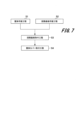
- the electromagnetic wave shielding material 40 is formed on the housing base 15 in the housing manufacturing process S1 described above.
- the housing manufacturing process S1 corresponds to a process of forming the electromagnetic wave shielding material 40 on the housing (the housing base 15 in this embodiment).
- the electromagnetic wave shielding material 40 is provided in a state of being adhered to the surface of the shielding base 39 of the housing base 15.
- the electromagnetic wave shielding material 40 is formed in a state of protruding toward the circuit board 11 side.
- Such an electromagnetic wave shielding material 40 is formed, for example, by the following method in the housing manufacturing process S1 described above. First, the housing base 15 is manufactured by the housing base manufacturing process.
- the ground pattern 26 has a first ground pattern portion 26a, a second ground pattern portion 26b, and a third ground pattern portion 26c.
- the first ground pattern portion 26a, the second ground pattern portion 26b, and the third ground pattern portion 26c are arranged in a position facing the shielding base 39 of the housing base 15.
- the second ground pattern portion 26b and the third ground pattern portion 26c are arranged in a position adjacent to the first ground pattern portion 26a with the first ground pattern portion 26a sandwiched therebetween.
- a predetermined interval is provided between the first ground pattern portion 26a and the second ground pattern portion 26b, and a predetermined interval is also provided between the first ground pattern portion 26a and the third ground pattern portion 26c.
- the first ground pattern portion 26a, the second ground pattern portion 26b, and the third ground pattern portion 26c are formed on the circuit board 11 as independent pattern portions.
- the electromagnetic wave shielding material 40 is in a state where the vicinity of the top 40a of the electromagnetic wave shielding material 40 is pressed against the pattern surface 41 of the first ground pattern portion 26a. Furthermore, the electromagnetic wave shielding material 40 is compressed and deformed by the pressing force applied when the circuit board 11 is attached to the housing base 15 in the circuit board attachment process S3 described above. Figure 6 shows the state of the electromagnetic wave shielding material 40 before it is compressed and deformed.
- each of the conductor protrusions 45, 46 By forming each of the conductor protrusions 45, 46 by soldering in this way, the solder can be formed simultaneously in the process of mounting various electronic components on the circuit board 11 by solder reflow. Therefore, there is no need to add a process for forming the conductor protrusions 45, 46. Therefore, the circuit board 11 on which the conductor protrusions 45, 46 are formed can be manufactured inexpensively.
- the electrical connection between the ground pattern 26 and the housing base 15 can be strengthened, and the electromagnetic wave shielding performance of the electromagnetic wave shielding material 40 can be improved.
- the conductivity of the conductor protrusion is higher than that of the electromagnetic wave shielding material even when the conductor protrusion is made of a material other than solder, specifically, a metal such as copper or aluminum.
- FIG. 8 is a perspective view showing an arrangement of an electromagnetic wave shielding material and a ground pattern in the electronic control device according to the first embodiment.
- the conductor protrusion 46 is formed along the ground pattern 26.
- the conductor protrusion 45 is formed along the ground pattern 26. Therefore, the length direction of each of the conductor protrusions 45, 46 is the same as the length direction Y of the ground pattern 26. Furthermore, the width direction of each of the conductor protrusions 45, 46 is the same as the width direction X of the ground pattern 26.
- the conductor protrusion 45 is disposed on one side of the ground pattern 26 in the width direction X, and the conductor protrusion 46 is disposed on the other side of the ground pattern 26 in the width direction X.
- the electromagnetic shielding material 40 is arranged in contact with the pattern surface 41 of the ground pattern 26 and the conductor protrusions 45, 46.
- the conductor protrusion 45 is in contact with the side portion 40b of the electromagnetic shielding material 40 that is shifted to one side (left side in FIG. 6) from the top of the electromagnetic shielding material 40.
- the conductor protrusion 46 is in contact with the side portion 40c of the electromagnetic shielding material 40 that is shifted to the other side (right side in FIG. 6) from the top 40a of the electromagnetic shielding material 40.
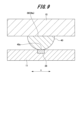
- the following advantages can be obtained compared to a configuration in which the electromagnetic shielding material 40 formed on the housing base 15 is pressed against the ground pattern 26 of the circuit board 11 to electrically connect the ground pattern 26 to the housing base 15, as in the comparative example shown in FIG. 9.
- the contact area of the electromagnetic shielding material 40 with the first ground pattern portion 26a is enlarged.
- the contact area of the electromagnetic shielding material 40 with the conductor protrusion 45 on the second ground pattern portion 26b and the contact area of the electromagnetic shielding material 40 with the conductor protrusion 46 on the third ground pattern portion 26c are both enlarged.
- the contact area of the electromagnetic shielding material 40 with the ground pattern 26 can be substantially enlarged.
- the electromagnetic shielding material 40 is electrically connected to the first ground pattern portion 26a, electrically connected to the second ground pattern portion 26b via the conductor protrusion 45, and electrically connected to the third ground pattern portion 26c via the conductor protrusion 46. Therefore, the electrical connection between the housing base 15 and the ground pattern 26 can be strengthened. As a result, the ground around the circuit area 25 of the circuit board 11 can be strengthened, and the electromagnetic noise shielding performance of the electromagnetic shielding material 40 can be improved.
- Fig. 10 is a perspective view showing a part of a circuit board 11 included in an electronic control device according to the second embodiment.
- Fig. 11 is a front view showing a part of a circuit board 11 included in an electronic control device according to the second embodiment.
- Fig. 10 and Fig. 11 both show the structure of the circuit board 11 at the portion against which the electromagnetic wave shielding material 40 is pressed.
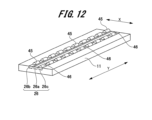
- the ground pattern 26 of the circuit board 11 has a first ground pattern portion 26a, a second ground pattern portion 26b, and a third ground pattern portion 26c.
- each of the conductor protrusions 45, 46 is formed linearly and continuously with the same length as the ground pattern 26.
- each of the conductor protrusions 45, 46 is formed in a plurality of portions at predetermined intervals in the longitudinal direction Y of the ground pattern 26.
- each of the conductor protrusions 45, 46 is formed by dividing it into a plurality of portions in the longitudinal direction Y of the ground pattern 26.
- Such a circuit board 11 can be obtained by changing the position, size, and number of openings of a mask used to apply solder paste to the second ground pattern portion 26b and the third ground pattern portion 26c in the circuit board manufacturing process S2 described above.
- the multiple conductor protrusions 45 are arranged on one side of the ground pattern 26 in the width direction X (upper side in FIG. 11).
- the multiple conductor protrusions 46 are arranged on the other side of the ground pattern 26 in the width direction X (lower side in FIG. 11).
- the multiple conductor protrusions 45 and the multiple conductor protrusions 46 are also arranged at the same positions as each other in the length direction Y of the ground pattern 26. Therefore, when viewed from the width direction X of the ground pattern 26, the multiple conductor protrusions 45 and the multiple conductor protrusions 46 are arranged to overlap each other.
- each of the conductor protrusions 45, 46 By forming each of the conductor protrusions 45, 46 at a predetermined interval in the longitudinal direction Y of the ground pattern 26 in this manner, the amount of material used to construct the conductor protrusions 45, 46 can be reduced compared to the first embodiment described above. Therefore, high shielding performance can be ensured at low cost.
- the first ground pattern portion 26a of the ground pattern 26 has a recess 47.
- the recess 47 is formed in a state where it is recessed from the pattern surface 41 of the first ground pattern portion 26a.
- the shape of the recess 47 in FIG. 14 shows the cross-sectional shape of the recess 47.
- the surface of the recess 47 corresponds to the conductor reference surface.
- the recess 47 is formed by machining a part of the first ground pattern portion 26a after the pattern formation process in the circuit board manufacturing process S2 (see FIG. 7) described above.
- the recess 47 is formed at a location where the electromagnetic wave shielding material 40 comes into contact.
- the recess 47 is formed at a location where the top of the electromagnetic wave shielding material 40 protruding in a semicircular shape comes into contact.
- the recess 47 is formed continuously along the length direction Y of the ground pattern 26 (see FIG. 8).
- the recess 47 may be formed intermittently (discontinuously) at a predetermined interval in the length direction Y of the ground pattern 26.
- the top of the electromagnetic shielding material 40 is pressed into the recess 47 by the pressing force F that is generated when the circuit board 11 is attached to the housing base 15.
- the top of the electromagnetic shielding material 40 deforms to fit the shape of the recess 47 due to the compressive deformation of the electromagnetic shielding material 40. This increases the contact area of the electromagnetic shielding material 40 with the first ground pattern portion 26a. This ensures higher shielding performance.
- FIG. 15 is an enlarged cross-sectional view showing the arrangement of a circuit board 11, a housing base 15, and an electromagnetic wave shielding material 40 provided in an electronic control device according to the fifth embodiment.
- the top of the electromagnetic shielding material 40 easily conforms to the shape of the recess 47 when the top of the electromagnetic shielding material 40 is pressed into the recess 47 by the above-mentioned pressing force F. This increases the contact area of the electromagnetic shielding material 40 with the first ground pattern portion 26a, ensuring higher shielding performance.
- the conductor protrusions 51, 52 are formed by fixing copper blocks to the second ground pattern portion 26b and the third ground pattern portion 26c by soldering after the pattern formation process in the circuit board fabrication process S2 described above (see FIG. 7).
- the copper blocks are also fabricated by, for example, cutting before the above-mentioned soldering.
- a conductor protrusion 51 is formed on the second ground pattern portion 26b, and a conductor protrusion 52 is formed on the third ground pattern portion 26c. Both conductor protrusions 51 and 52 are formed from copper blocks.
- the shapes of conductor protrusions 51 and 52 in FIG. 18 show the cross-sectional shapes of conductor protrusions 51 and 52.
- the method of forming conductor protrusions 51 and 52 is basically the same as in the seventh embodiment described above.
- the pattern recess 55 is formed by recessing the center of the ground pattern 26 in the width direction X into a substantially U-shape (concave shape). Therefore, the thickness dimension of the ground pattern 26 is smaller in the center of the ground pattern 26 than in other parts.
- the pattern recess 55 is formed continuously and long along the length of the ground pattern 26. However, the pattern recess 55 may be formed intermittently (discontinuously) at a predetermined interval in the length of the ground pattern 26.
- the width W3 of the pattern recess 55 is narrower than the width W2 of the electromagnetic wave shielding material 40.
- the width W1 of the ground pattern 26, the width W2 of the electromagnetic wave shielding material 40, and the width W3 of the pattern recess 55 are all dimensions defined in the width direction X of the ground pattern 26.
- the bottom surface 55a of the pattern recess 55 corresponds to the conductor reference surface
- the top surface 26d of the ground pattern 26 corresponds to the conductor protrusion.
- the pattern recess 55 is formed in the ground pattern 26, and the central part of the ground pattern 26 in the width direction X is recessed due to the presence of this pattern recess 55, so that the bottom surface 55a as the conductor reference surface and the top surface 26d as the conductor protrusion are formed integrally (integral structure) with the ground pattern 26.
- the cross-sectional shape of the pattern recess 55 is not limited to an approximately U-shape, but may be, for example, a semicircular shape or an approximately V-shape.
- the width W1 of the ground pattern 26 is equal to or greater than the width W2 of the electromagnetic wave shielding material 40.
- the electronic control device according to the tenth embodiment is partially different from the above-described ninth embodiment in the structure of the ground pattern 26.
- 20 is an enlarged cross-sectional view showing the arrangement of the circuit board 11, the housing base 15, and the electromagnetic shielding material 40 included in the electronic control device according to the tenth embodiment.
- the shape of the ground pattern 26 in FIG. 20 shows the cross-sectional shape of the ground pattern 26.
- the ground pattern 26 has a pattern recess 55 in the center of the width direction X of the ground pattern 26. This is the same as the ninth embodiment, including the method of forming the pattern recess 55.
- the upper surface 26d of the ground pattern 26 forms a plane that is substantially flush with the main surface 11a of the circuit board 11.
- the upper surface 26d of the ground pattern 26 is disposed so as to protrude toward the electromagnetic wave shielding material 40 (housing base 15) side from the main surface 11a of the circuit board 11.
- the pattern convex portion 56 may be divided into multiple portions at a predetermined interval in the length direction of the ground pattern 26.
- the pattern convex portion 56 is formed in a convex shape in a state where it protrudes toward the electromagnetic wave shielding material 40 side from the upper surface (main surface) 26e of the ground pattern 26.
- the top surface 26e (main surface) of the ground pattern 26 is arranged in pairs on both sides of the pattern protrusion 56 when viewed from the longitudinal direction of the ground pattern 26.
- the top surface 26e of the ground pattern 26 forms a plane that is substantially the same as the main surface 11a of the circuit board 11.
- the top surface 26e of the ground pattern 26 corresponds to the conductor reference plane
- the pattern protrusion 56 of the ground pattern 26 corresponds to the conductor protrusion.
- the pattern protrusion 56 is formed in the ground pattern 26, and the central portion of the ground pattern 26 in the width direction X is protruded by the presence of this pattern protrusion 56, so that the top surface 26e as the conductor reference plane and the pattern protrusion 56 as the conductor protrusion are formed integrally with the ground pattern 26.
- the contact area of the electromagnetic shielding material 40 with the ground pattern 26 can be enlarged, and the electrical connection between the housing base 15 and the ground pattern 26 can be strengthened. Therefore, the electromagnetic noise shielding performance of the electromagnetic shielding material 40 can be improved.
- the pattern protrusions 56 bite into the electromagnetic shielding material 40, thereby restricting the movement of the electromagnetic shielding material 40 in the width direction X of the ground pattern 26. As a result, it is possible to suppress the positional deviation of the electromagnetic shielding material 40 in the width direction X of the ground pattern 26.
- the electronic control device according to the twelfth embodiment is different from the above-described eleventh embodiment in the number of pattern protrusions 56 provided on the ground pattern 26 .
- 22 is an enlarged cross-sectional view showing the arrangement of the circuit board 11, the housing base 15, and the electromagnetic shielding material 40 included in the electronic control device according to the twelfth embodiment.
- the shape of the ground pattern 26 in FIG. 22 shows the cross-sectional shape of the ground pattern 26.
- the ground pattern 26 has a plurality of pattern protrusions 56 (56a, 56b, 56c, 56d, 56e).
- five pattern protrusions 56a, 56b, 56c, 56d, 56e are provided on the ground pattern 26.
- the five pattern protrusions 56a, 56b, 56c, 56d, 56e are formed integrally with the ground pattern 26 by protruding multiple locations in the width direction X of the ground pattern 26.
- the five pattern protrusions 56a, 56b, 56c, 56d, 56e are formed at predetermined intervals in the width direction X of the ground pattern 26.
- the five pattern convex portions 56a, 56b, 56c, 56d, and 56e are formed by, for example, cutting the ground pattern 26 so as to leave the five pattern convex portions 56a, 56b, 56c, 56d, and 56e after the pattern formation process in the circuit board fabrication process S2 described above (see FIG. 7).
- the pattern convex portion 56c is formed in the center of the ground pattern 26 in the width direction X.
- the pattern convex portions 56a and 56e are formed at both ends of the ground pattern 26 in the width direction X.
- the pattern convex portion 56b is formed between the pattern convex portions 56a and 56c in the width direction X of the ground pattern 26.
- the pattern convex portion 56d is formed between the pattern convex portions 56c and 56e in the width direction X of the ground pattern 26.
- the multiple pattern protrusions 56 (56a, 56b, 56c, 56d, and 56e) in the ground pattern 26 in this way, the upper surface 26e of the ground pattern 26 as the conductor reference surface and the multiple pattern protrusions 56 (56a, 56b, 56c, 56d, and 56e) as the conductor protrusions are formed integrally with the ground pattern 26.
- the pattern convex portion 56c when the electromagnetic shielding material 40 is pressed against the ground pattern 26 by the pressing force generated when the circuit board 11 is attached to the housing base 15, the pattern convex portion 56c is in a state of being embedded in the top of the electromagnetic shielding material 40.
- the pattern convex portion 56b is in a state of being embedded in one side portion (left side in FIG. 22) of the electromagnetic shielding material 40, and the pattern convex portion 56d is in a state of being embedded in the other side portion (right side in FIG. 22) of the electromagnetic shielding material 40.
- five pattern protrusions 56 are formed on the ground pattern 26, but the number of pattern protrusions 56 may be two or more.
- FIG. 23 is an enlarged cross-sectional view showing the arrangement of a circuit board 11, a housing base 15, and an electromagnetic wave shielding material 60 provided in an electronic control device according to the thirteenth embodiment.
- the electromagnetic shielding material 60 is disposed between the ground pattern 26 of the circuit board 11 and the shielding seat 39 of the housing base 15.
- the ground pattern 26 is formed to be wider than the ground pattern 26 in the comparative example (FIG. 9).
- the electromagnetic shielding material 60 is formed in a semicircular shape when viewed from the longitudinal direction of the ground pattern 26.
- the shape of the electromagnetic shielding material 60 in FIG. 23 shows the cross-sectional shape of the electromagnetic shielding material 60.
- the shape of the electromagnetic shielding material 60 in FIG. 23 shows the shape before the electromagnetic shielding material 60 is compressed and deformed.
- the electromagnetic shielding material 60 is formed on the ground pattern 26 of the circuit board 11.
- the electromagnetic shielding material 60 is provided in a state of being adhered to the upper surface (front surface) 26f of the ground pattern 26.
- the electromagnetic shielding material 60 is formed in a state of protruding toward the housing base 15 in the thickness direction of the circuit board 11.
- Such an electromagnetic wave shielding material 60 is formed on the circuit board 11 in the circuit board manufacturing process S2 (see FIG. 7) described above, for example, by the following method.
- the circuit board 11 on which the pattern forming process has been completed is prepared.
- a liquid or paste-like material (conductive adhesive) containing a conductive filler which is the raw material of the electromagnetic wave shielding material 60, is applied to the surface of the ground pattern 26 of the circuit board 11 using a coating nozzle (not shown).
- the material on the ground pattern 26 is hardened, for example, by moisture, heat, ultraviolet light irradiation, etc.
- the method for hardening the material applied to the ground pattern 26 of the circuit board 11 is determined by the properties (moisture hardening, heat hardening, ultraviolet light hardening, etc.) of the material used as the raw material of the electromagnetic wave shielding material 40.
- the electromagnetic wave shielding material 60 is formed in a semicircular protruding state.
- the electromagnetic wave shielding material 60 has rubber-like elasticity by being made of the same material as the electromagnetic wave shielding material 40 in the first embodiment.
- the circuit board manufacturing process S2 corresponds to the process of forming the electromagnetic wave shielding material 60 on the circuit board 11.
- the housing base 15 is provided with two conductor protrusions 61, 62.
- Each of the conductor protrusions 61, 62 is formed by partially protruding the housing base 15 in a convex shape. Therefore, each of the conductor protrusions 61, 62 can be referred to as a housing protrusion.
- the conductor protrusions 61, 62 are formed integrally with the housing base 15 by protruding a part of a specific surface of the housing base 15 arranged in a state facing the ground pattern 26. Specifically, the conductor protrusions 61, 62 are provided in a state of protruding from the surface 39a of the shielding base 39.
- the surface 39a of the shielding base 39 corresponds to the conductor reference surface.
- the conductor protrusions 61, 62 are formed integrally (integral structure) with the housing base 15. This allows the housing base 15 to be manufactured at a lower cost than when the conductor protrusions are formed separately (as separate structures) on the housing base 15.
- the two conductor protrusions 61, 62 may be formed in the housing base manufacturing process S1 (see FIG. 7) described above, or may be formed by performing post-processing such as cutting on the housing base 15 obtained by the housing base manufacturing process.
- the housing manufacturing process S1 corresponds to a process of forming the conductor reference surface and the conductor protrusions on the housing (housing base 15 in this embodiment).
- the conductor protrusions 61, 52 are arranged in pairs in the width direction X of the ground pattern 26.
- Each of the conductor protrusions 61, 62 is formed at a position facing both ends of the ground pattern 26 in the width direction X.
- each of the conductor protrusions 61, 62 is formed in a state in which a part of the surface 39a of the shield base 39 protrudes toward the electromagnetic wave shielding material 60 side (circuit board 11 side) in the thickness direction of the housing base 15. Therefore, the conductor protrusions 61, 62 protrude toward the electromagnetic wave shielding material 60 side (circuit board 11 side) more than the surface 39a of the shield base 39.
- the surface 39a of the shield base 39 corresponds to a predetermined surface of the housing that is arranged in a state facing the ground pattern 26.
- Each of the conductor protrusions 61, 62 is formed long and continuous along the ground pattern 26 in the length direction of the ground pattern 26 (depth direction in FIG. 23). However, each of the conductor protrusions 61, 62 may be divided into multiple parts at a predetermined interval in the longitudinal direction of the ground pattern 26. Also, each of the conductor protrusions 61, 62 is formed in a convex shape. The shapes of the conductor protrusions 61, 62 in FIG. 23 show the cross-sectional shapes of the conductor protrusions 61, 62 when viewed from the longitudinal direction of the ground pattern 26.
- each of the conductor protrusions 61, 62 may be, for example, a trapezoid or a triangle in order to form the side of each of the conductor protrusions 61, 62 in a tapered shape. This makes it easier for the side portions 60b, 60c of the electromagnetic shielding material 60 to fit the side of the corresponding conductor protrusions 61, 62 when the electromagnetic shielding material 60 is pressed against the shielding base 39. This increases the contact area of the electromagnetic shielding material 60 with the housing base 15, ensuring higher shielding performance.
- the housing base 15 has a housing recess 65.
- the housing recess 65 may be formed in the housing base manufacturing process S1 (see FIG. 7) described above, or may be formed by performing post-processing such as cutting on the housing base 15 obtained in the housing base manufacturing process.
- the housing recess 65 is formed by recessing a part of the surface 39b of the shield base 39 into a substantially U-shape.
- the housing recess 65 is formed integrally with the housing base 15.
- the housing recess 65 is formed in a state facing the ground pattern 26.
- the surface 39b of the shield base 39 is disposed in a state protruding toward the electromagnetic wave shielding material 60 side more than the bottom surface 65a of the housing recess 65.
- the electromagnetic shielding material 60 is compressively deformed (elastically deformed) by the pressing force F that is generated when the circuit board 11 is attached to the housing base 15.
- the vicinity of the top of the electromagnetic shielding material 60 contacts the bottom surface 65a of the housing recess 65, and the side portion of the electromagnetic shielding material 60 contacts the surface 39b of the shield base 39. Therefore, the same effect as in the 13th embodiment can be obtained.
- the conductor protrusion 66 is formed in a state where it protrudes toward the electromagnetic wave shielding material 60 side (circuit board 11 side) more than the surface 39c of the shield base 39.
- the surface 39c of the shield base 39 corresponds to a predetermined surface of the housing that is arranged in a state facing the ground pattern 26.
- the surface 39c of the shield base 39 corresponds to a conductor reference surface.
- the conductor protrusion 66 is formed continuously and elongated along the ground pattern 26 in the longitudinal direction of the ground pattern 26 (depth direction in FIG. 25). However, the conductor protrusion 66 may be divided into multiple parts at predetermined intervals in the longitudinal direction of the ground pattern 26.
- the conductor protrusion 66 is formed in a convex shape.
- the shape of the conductor protrusion 66 in FIG. 25 shows the cross-sectional shape of the conductor protrusion 66 when viewed in the longitudinal direction of the ground pattern 26.
- the conductor protrusion 66 bites into the electromagnetic shielding material 60, thereby restricting the movement of the electromagnetic shielding material 60 in the width direction X of the ground pattern 26. As a result, it is possible to suppress the positional deviation of the electromagnetic shielding material 60 in the width direction X of the ground pattern 26.
- the housing base 15 has a plurality of conductor protrusions 66 (66a, 66b, 66c, 66d, 66e).
- five conductor protrusions 66a, 66b, 66c, 66d, 66e are provided on the housing base 15.
- the five conductor protrusions 66a, 66b, 66c, 66d, 66e are arranged at a predetermined interval in the width direction X of the ground pattern 26.
- the five conductor protrusions 66a, 66b, 66c, 66d, 66e may be formed by the housing base manufacturing process in the housing manufacturing process S1 described above (see FIG.
- Each of the conductor protrusions 66a, 66b, 66c, 66d, and 66e is formed so as to protrude further toward the electromagnetic wave shielding material 60 than the surface 39c of the shield base 39.
- the surface 39c of the shield base 39 is formed between two adjacent conductor protrusions in the width direction X of the ground pattern 26.
- the surface 39c of the shield base 39 can be rephrased as a concave bottom surface formed between two adjacent conductor protrusions in the width direction X of the ground pattern 26.
- the electromagnetic shielding material 60 when the electromagnetic shielding material 60 is pressed against the shielding base 39 of the housing base 15 by the above-mentioned pressing force, at least three conductor protrusions 66b, 66c, and 66d bite into the electromagnetic shielding material 60, thereby restricting the movement of the electromagnetic shielding material 60 in the width direction X of the ground pattern 26. As a result, it is possible to suppress the positional deviation of the electromagnetic shielding material 60 in the width direction X of the ground pattern 26.
- five conductor protrusions 66 (66a, 66b, 66c, 66d, 66e) are formed on the housing base 15, but the number of conductor protrusions 66 may be two or more.
- the ground pattern 26 is formed so as to surround the circuit area 25 on all four sides as shown in FIG. 4 above, but the present invention is not limited to this, and the ground pattern 26 may be formed so as to surround the circuit area 25 on three sides.
Landscapes
- Engineering & Computer Science (AREA)
- Microelectronics & Electronic Packaging (AREA)
- Shielding Devices Or Components To Electric Or Magnetic Fields (AREA)
Priority Applications (3)
| Application Number | Priority Date | Filing Date | Title |
|---|---|---|---|
| CN202380101901.7A CN121753492A (zh) | 2023-10-10 | 2023-10-10 | 电子控制装置和电子控制装置的制造方法 |
| JP2025551227A JPWO2025079129A1 (https=) | 2023-10-10 | 2023-10-10 | |
| PCT/JP2023/036694 WO2025079129A1 (ja) | 2023-10-10 | 2023-10-10 | 電子制御装置、及び、電子制御装置の製造方法 |
Applications Claiming Priority (1)
| Application Number | Priority Date | Filing Date | Title |
|---|---|---|---|
| PCT/JP2023/036694 WO2025079129A1 (ja) | 2023-10-10 | 2023-10-10 | 電子制御装置、及び、電子制御装置の製造方法 |
Publications (1)
| Publication Number | Publication Date |
|---|---|
| WO2025079129A1 true WO2025079129A1 (ja) | 2025-04-17 |
Family
ID=95395310
Family Applications (1)
| Application Number | Title | Priority Date | Filing Date |
|---|---|---|---|
| PCT/JP2023/036694 Pending WO2025079129A1 (ja) | 2023-10-10 | 2023-10-10 | 電子制御装置、及び、電子制御装置の製造方法 |
Country Status (3)
| Country | Link |
|---|---|
| JP (1) | JPWO2025079129A1 (https=) |
| CN (1) | CN121753492A (https=) |
| WO (1) | WO2025079129A1 (https=) |
Citations (3)
| Publication number | Priority date | Publication date | Assignee | Title |
|---|---|---|---|---|
| JPH0195069U (https=) * | 1987-12-17 | 1989-06-22 | ||
| JPH0613195U (ja) * | 1992-07-24 | 1994-02-18 | ユピテル工業株式会社 | シールドボックスへの基板の保持構造 |
| JPH10107476A (ja) * | 1996-09-27 | 1998-04-24 | New Japan Radio Co Ltd | 高周波回路基板の接地及び電波シールド構造 |
-
2023
- 2023-10-10 JP JP2025551227A patent/JPWO2025079129A1/ja active Pending
- 2023-10-10 WO PCT/JP2023/036694 patent/WO2025079129A1/ja active Pending
- 2023-10-10 CN CN202380101901.7A patent/CN121753492A/zh active Pending
Patent Citations (3)
| Publication number | Priority date | Publication date | Assignee | Title |
|---|---|---|---|---|
| JPH0195069U (https=) * | 1987-12-17 | 1989-06-22 | ||
| JPH0613195U (ja) * | 1992-07-24 | 1994-02-18 | ユピテル工業株式会社 | シールドボックスへの基板の保持構造 |
| JPH10107476A (ja) * | 1996-09-27 | 1998-04-24 | New Japan Radio Co Ltd | 高周波回路基板の接地及び電波シールド構造 |
Also Published As
| Publication number | Publication date |
|---|---|
| JPWO2025079129A1 (https=) | 2025-04-17 |
| CN121753492A (zh) | 2026-03-27 |
Similar Documents
| Publication | Publication Date | Title |
|---|---|---|
| JP4470980B2 (ja) | 電子装置 | |
| CN1285247C (zh) | 电磁屏蔽板、电磁屏蔽结构件和娱乐装置 | |
| JP5632898B2 (ja) | 機械的構造物により把持され固定される回路基板、及びこれを用いた制御装置 | |
| JP2003124662A (ja) | 車載電子機器 | |
| US20150207216A1 (en) | Wireless module | |
| CN1302694C (zh) | 被冷却的电开关装置 | |
| JP2002216886A (ja) | 車載電子機器 | |
| US7244141B2 (en) | Electric connector box | |
| DE102014207039B4 (de) | Elektronische Steuereinheit | |
| JP2009295706A (ja) | 電子制御装置 | |
| WO2025079129A1 (ja) | 電子制御装置、及び、電子制御装置の製造方法 | |
| JP2013149899A (ja) | 電子制御ユニットのケース | |
| JP5239926B2 (ja) | 電子装置及びその製造方法 | |
| JP2019036678A (ja) | 電子装置 | |
| US6178095B1 (en) | Structure for fixing an element to a printed wiring board, and electronic equipment having the structure | |
| JP4876906B2 (ja) | 三次元基板間接続構造体およびそれを用いた立体回路装置 | |
| JP7598482B2 (ja) | 電子制御装置 | |
| JP2000012129A (ja) | 基板取り付けコネクタ構成部材、基板取り付けコネクタ対およびコネクタ接続構造 | |
| US20250365908A1 (en) | Electronic control device and method for manufacturing electronic control device | |
| WO2021070569A1 (ja) | 電子機器 | |
| JP2024125736A (ja) | シールド構造を有する電子機器、及び電子機器の製造方法 | |
| JP6475502B2 (ja) | 機械的構造物により把持されて固定される回路基板、及びこれを用いた電子装置 | |
| CN216596157U (zh) | 电脑水冷散热装置 | |
| JP2007066575A (ja) | コネクタの実装構造及び実装方法 | |
| JP2023127764A (ja) | 電子制御装置 |
Legal Events
| Date | Code | Title | Description |
|---|---|---|---|
| 121 | Ep: the epo has been informed by wipo that ep was designated in this application |
Ref document number: 23955381 Country of ref document: EP Kind code of ref document: A1 |
|
| ENP | Entry into the national phase |
Ref document number: 2025551227 Country of ref document: JP Kind code of ref document: A |