WO2025062637A1 - 半導体装置 - Google Patents
半導体装置 Download PDFInfo
- Publication number
- WO2025062637A1 WO2025062637A1 PCT/JP2023/034522 JP2023034522W WO2025062637A1 WO 2025062637 A1 WO2025062637 A1 WO 2025062637A1 JP 2023034522 W JP2023034522 W JP 2023034522W WO 2025062637 A1 WO2025062637 A1 WO 2025062637A1
- Authority
- WO
- WIPO (PCT)
- Prior art keywords
- semiconductor device
- electrode
- conductive portion
- substrate
- recess
- Prior art date
- Legal status (The legal status is an assumption and is not a legal conclusion. Google has not performed a legal analysis and makes no representation as to the accuracy of the status listed.)
- Pending
Links
Images






Classifications
-
- H—ELECTRICITY
- H10—SEMICONDUCTOR DEVICES; ELECTRIC SOLID-STATE DEVICES NOT OTHERWISE PROVIDED FOR
- H10W—GENERIC PACKAGES, INTERCONNECTIONS, CONNECTORS OR OTHER CONSTRUCTIONAL DETAILS OF DEVICES COVERED BY CLASS H10
- H10W70/00—Package substrates; Interposers; Redistribution layers [RDL]
- H10W70/60—Insulating or insulated package substrates; Interposers; Redistribution layers
Definitions
- This disclosure relates to a semiconductor device.
- JP 2013-89948 A there is known a semiconductor device that uses flip-chip mounting in which a mounting substrate is connected to an electrode of a semiconductor substrate so that the back surface of the semiconductor substrate faces the mounting substrate (see, for example, JP 2013-89948 A).
- the semiconductor substrate has a guard ring as an electric field strength mitigation section that mitigates the high electric field generated in the active region.
- the semiconductor device includes a semiconductor substrate and a mounting substrate.
- the semiconductor substrate has a first surface.
- the mounting substrate has a main surface. The main surface faces the first surface.
- An electric field strength mitigation portion and an electrode are formed on the first surface.
- the electrode is connected to the mounting substrate.
- a recess is formed on the main surface. The recess is disposed at a position overlapping the electric field strength mitigation portion in a plan view of the first surface.
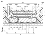
- 1 is a schematic cross-sectional view of a semiconductor device according to a first embodiment
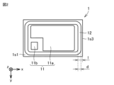
- 2 is a schematic bottom view of a semiconductor substrate in the semiconductor device according to the first embodiment
- 1 is a schematic plan view of a mounting substrate in a semiconductor device according to a first embodiment
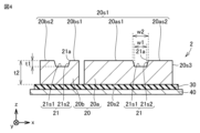
- 4 is a schematic cross-sectional view taken along line IV-IV in FIG. 3.
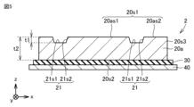
- 4 is a schematic cross-sectional view taken along line VV in FIG. 3.
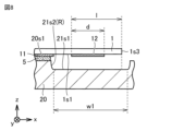
- 3 is a schematic partial cross-sectional view of a recess in the semiconductor device according to the first embodiment
- 10 is a schematic partial cross-sectional view of a modified example of a recess in the semiconductor device according to the first embodiment.
- FIG. 10 is a schematic partial cross-sectional view of a modified example of a recess in the semiconductor device according to the first embodiment.
- FIG. 10 is a schematic partial cross-sectional view of a modified example of a recess in the semiconductor device according to the first embodiment.
- FIG. 2 is a schematic plan view showing a conductive portion in the semiconductor device according to the first embodiment;
- 11 is a schematic cross-sectional view taken along line XI-XI in FIG. 10 .
- FIG. 17 is a schematic cross-sectional view taken along line XVII-XVII in FIG. 16.
- FIG. 11 is a schematic cross-sectional view of a semiconductor device according to a third embodiment.
- FIG. 11 is a schematic cross-sectional view of a semiconductor device according to a fourth embodiment.
- FIG. 13 is a schematic cross-sectional view of a semiconductor device according to a fifth embodiment.
- FIG. 13 is a schematic cross-sectional view of a modified example of the semiconductor device according to the fifth embodiment.
- FIG 1 is a schematic cross-sectional view of a semiconductor device 100a according to a first embodiment.
- FIG 2 is a schematic bottom view of a semiconductor substrate 1 in the semiconductor device 100a according to the first embodiment.
- FIG 3 is a schematic plan view of a mounting substrate 2 in the semiconductor device 100a according to the first embodiment.
- FIG 4 is a schematic cross-sectional view taken along line IV-IV in FIG 3.
- FIG 5 is a schematic cross-sectional view taken along line V-V in FIG 3.
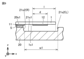
- FIG 6 is a schematic partial cross-sectional view of an electric field intensity mitigating portion 12 and a recess 21 in the semiconductor device 100a according to the first embodiment.
- the semiconductor device 100a shown in Figures 1 to 6 is, for example, a power semiconductor device 100a, and mainly comprises a semiconductor substrate 1, a mounting substrate 2, a joint 5, a wiring circuit 6, and a sealing resin 7.
- the joint 5 includes a first joint 5a, a second joint 5b, a third joint 5c, a fourth joint 5d, and a fifth joint 5e.
- the wiring circuit 6 includes a first wiring circuit 6a, a second wiring circuit 6b, and a third wiring circuit 6c.
- the semiconductor substrate 1 has a first surface 1s1, a second surface 1s2, and a third surface 1s3.
- the first surface 1s1 is the surface facing the main surface 20s1 of the mounting substrate 2.
- the second surface 1s2 is the surface opposite the first surface 1s1.
- the third surface 1s3 connects the first surface 1s1 and the second surface 1s2.
- the first surface 1s1 is the back surface of the semiconductor substrate 1.
- the second surface 1s2 is the front surface of the semiconductor substrate 1.
- the third surface 1s3 is the side surface of the semiconductor substrate 1.
- the first surface 1s1 and the second surface 1s2 extend in the x direction and the y direction perpendicular to the x direction.
- the x direction is the direction in which the wiring circuit extends.
- the y direction is perpendicular to the x direction.
- the z direction is the thickness direction of the semiconductor substrate 1.
- the normal direction of the first surface 1s1 is the z direction.
- the second surface 1s2 faces the +z direction.
- the first surface 1s1 faces the -z direction.
- the shape of the electric field strength mitigation section 12 does not have to be annular.
- the electric field strength mitigation section 12 may be a termination structure called a JTE (Junction Termination Extension) structure.
- the electric field strength mitigation section 12 may be, for example, a p-type region formed by ion implantation.
- the electrode 11 includes a first electrode 11a and a second electrode 11b.
- the first electrode 11a is a main electrode.
- a main current flows through the main electrode.
- the second electrode 11b is a control electrode.
- the control electrode controls the main current.
- the first electrode 11a and the second electrode 11b are disposed spaced apart from each other on the first surface 1s1.
- the first electrode 11a is connected to the mounting substrate 2 via the first joint 5a.
- the second electrode 11b is connected to the mounting substrate 2 via the second joint 5b.
- an upper electrode 11u is formed on the second surface 1s2 of the semiconductor substrate 1.
- a main current flows through the upper electrode 11u.
- a third wiring circuit 6c is connected to the upper electrode 11u via a fifth joint 5e.
- the third wiring circuit 6c extends in the x-direction.
- the semiconductor substrate 1 is a so-called power semiconductor substrate 1 that controls power. Any material may be used as the material for forming the semiconductor substrate 1. Materials such as silicon (Si), silicon carbide (SiC), gallium nitride (GaN), and gallium oxide (GaO) may be used as the material for forming the semiconductor substrate 1.
- the material constituting the electrode 11 is preferably a material having high electrical and thermal conductivity.
- the material constituting the electrode 11 may include, for example, any of aluminum (Al), an aluminum alloy, copper (Cu), and a copper alloy.
- the electrode 11 may have a two-layer structure of Al/Cu, or a multi-layer structure including any of gold (Au) and silver (Ag).
- the electrode 11 may include a diffusion prevention layer.
- the diffusion prevention layer may include, for example, titanium (Ti) or the like.
- Nickel (Ni) silicide may be used as an underlayer for the electrode 11 to make ohmic contact with the semiconductor substrate 1.
- the electrode 11 may include a thin surface layer to prevent oxidation of the electrode 11 or to improve its bonding properties.
- the material constituting the surface layer is, for example, a precious metal such as gold.
- the electrodes 11 there are no particular restrictions on the electrodes 11.
- the locations of the first electrode 11a and the second electrode 11b there are no particular restrictions on the locations of the first electrode 11a and the second electrode 11b.
- the second electrode 11b may be disposed as a control electrode in a corner on the first surface 1s1, but it may also be disposed in the center of the first surface 1s1.
- the shape of the second electrode 11b may be any shape.
- the shape of the second electrode 11b may be a rectangle as shown in FIG. 2, or may be a circle, an ellipse, or a combination of an ellipse and a rectangle.
- the shape of the second electrode 11b may be a hexagon.
- the mounting substrate 2 has a conductive portion 20, a thermally conductive insulating layer 30, and a support layer 40.
- the conductive portion 20 has a front surface, a back surface 20s2, and a side surface 20s3.
- the front surface faces the first surface 1s1 of the semiconductor substrate 1.
- the main surface 20s1 of the mounting substrate 2 is composed of the front surface of the conductive portion 20.
- the back surface 20s2 is the surface opposite to the front surface of the conductive portion 20.
- the side surface 20s3 is a surface that connects the front surface and the back surface 20s2.
- the thermally conductive insulating layer 30 is connected to the back surface 20s2 of the conductive portion 20.
- the support layer 40 is connected to the surface of the thermally conductive insulating layer 30 opposite to the surface to which the conductive portion 20 is connected.
- the surface of the support layer 40 opposite to the surface to which the thermally conductive insulating layer 30 is connected is exposed from the sealing resin 7.
- the conductive portion 20 includes a first conductive portion 20a and a second conductive portion 20b.
- the first conductive portion 20a is disposed at a distance from the second conductive portion 20b. It is sufficient that the first conductive portion 20a and the second conductive portion 20b are insulated from each other. As shown in FIG. 1, it is preferable that the space between the first conductive portion 20a and the second conductive portion 20b is filled with an insulating material such as silicone gel or epoxy resin.
- the insulating material filled between the first conductive portion 20a and the second conductive portion 20b may be, for example, a sealing resin 7 as shown in FIG. 1.
- Insulating material may be filled between the first conductive portion 20a and the second conductive portion 20b at any stage in the manufacturing process of the semiconductor device 100a.
- insulating material may be filled between the first conductive portion 20a and the second conductive portion 20b at an early stage in the manufacturing process of the semiconductor device 100a.
- insulating material may be filled between the first conductive portion 20a and the second conductive portion 20b at a stage near the final process in the manufacturing process of the semiconductor device 100a.
- the insulating material filled between the first conductive portion 20a and the second conductive portion 20b is silicone gel, it is preferable to fill the insulating material after the semiconductor device 100a has been subjected to a process in which it is treated at high temperature.
- a recess 21 is formed on the main surface 20s1 of the mounting substrate 2. That is, the recess 21 is formed on the surface of the conductive portion 20.
- the main surface 20s1 includes a first electrode side surface 20as1 and a first wiring circuit side surface 20as2.
- the recess 21 is formed between the first electrode side surface 20as1 and the first wiring circuit side surface 20as2.
- the recess 21 is preferably filled with a sealing resin 7.
- the main surface 20s1 includes a second electrode side surface 20bs1 and a second wiring circuit side surface 20bs2.
- a recess 21 is formed between the second electrode side surface 20bs1 and the second wiring circuit side surface 20bs2.
- the conductive portion 20 is connected to the electrode 11. Specifically, the first electrode 11a is connected to the first electrode side surface 20as1 of the first conductive portion 20a via the first joint portion 5a. The second electrode 11b is connected to the second electrode side surface 20bs1 of the second conductive portion 20b via the second joint portion 5b.
- the first electrode 11a is disposed at a position overlapping the first electrode side surface 20as1 of the first conductive portion 20a.
- the second electrode 11b is disposed at a position overlapping the second electrode side surface 20bs1 of the second conductive portion 20b.
- the first wiring circuit 6a is connected to the first wiring circuit side 20as2 via the third joint 5c.
- the first wiring circuit 6a extends in the x direction.
- the second wiring circuit 6b is connected to the second wiring circuit side 20bs2 via the fourth joint 5d.
- the second wiring circuit 6b extends in the -x direction. In this way, the first electrode 11a, which is the main electrode, and the first conductive portion 20a are electrically and mechanically connected, and the second electrode 11b, which is the control electrode, and the second conductive portion 20b are electrically and mechanically connected.
- the material constituting the conductive portion 20 is preferably a material having high electrical and thermal conductivity.
- the material constituting the conductive portion 20 may include, for example, aluminum (Al), an aluminum alloy, copper (Cu), or a copper alloy.
- the thermally conductive insulating layer 30 is preferably made of a material having adhesive, electrical insulating, and thermally conductive functions.
- the material constituting the thermally conductive insulating layer 30 may be, for example, a thermosetting resin sheet containing an inorganic filler, an inorganic molded body sheet impregnated with a thermosetting resin, or a coating film.
- the thermally conductive insulating layer 30 fixes the first conductive portion 20a and the second conductive portion 20b, which are spaced apart from each other.
- a cooler (not shown) may be connected to the underside of the support layer 40.
- the support layer 40 may be made of a material capable of transferring heat to the cooler. Specifically, the material constituting the support layer 40 may be a thin metal plate or metal foil containing copper, aluminum, or an alloy thereof, which have high thermal conductivity.
- the support layer 40 also accounts for the majority of the mechanical strength of the semiconductor device 100a. For this reason, it is preferable that the support layer 40 has high mechanical strength.
- the conductive part 20, the thermally conductive insulating layer 30, and the support layer 40 are bonded together by the adhesive function of the thermally conductive insulating layer 30. Specifically, the conductive part 20, the thermally conductive insulating layer 30, and the support layer 40 are bonded together by applying pressure and heat.
- the members constituting the first wiring circuit 6a, the second wiring circuit 6b, and the third wiring circuit 6c may be, for example, conductive lead frames. It is preferable that the first wiring circuit 6a, the second wiring circuit 6b, and the third wiring circuit 6c are arranged parallel to the main surface 20s1. In particular, it is preferable that the first wiring circuit 6a and the third wiring circuit 6c have a flat plate shape. In this way, parasitic inductance is reduced.
- the sealing resin 7 covers the semiconductor substrate 1, the mounting substrate 2, a portion of the first wiring circuit 6a, a portion of the second wiring circuit 6b, and a portion of the third wiring circuit 6c. In this way, the insulation of the semiconductor device 100a is improved, and the effects of the external environment such as humidity and contamination can be reduced.
- the first wiring circuit 6a extends from the first wiring circuit side surface 20as2 of the first conductive portion 20a to the outside of the sealing resin 7.
- the second wiring circuit 6b extends from the second wiring circuit side surface 20bs2 of the second conductive portion 20b to the outside of the sealing resin 7.
- the third wiring circuit 6c extends from the second surface 1s2 of the semiconductor substrate 1 to the outside of the sealing resin 7.
- a portion of each of the first wiring circuit 6a, the second wiring circuit 6b, and the third wiring circuit 6c extends outward from the surface of the sealing resin 7 so as to be connectable to an external device outside the sealing resin 7.
- the first wiring circuit 6a, the second wiring circuit 6b, and the third wiring circuit 6c may be bent, for example, by forming, in the portions extending outward from the sealing resin 7.
- the material constituting the joint 5 can be solder. However, since solder has a relatively high thermal resistance, materials other than solder may be used to constitute the joint 5 of the semiconductor device 100a according to the first embodiment. Also, from the viewpoint of the long-term reliability of the joint 5, materials other than solder may be used.
- the thermal resistance is determined by the thermal conductivity, the joint thickness in the z direction, and the cross-sectional area of the joint 5 in the x and y directions.
- the third joint 5c, the fourth joint 5d, and the fifth joint 5e are formed using solder, remelting of the solder may occur depending on the process temperature and temperature profile during the manufacturing process of the semiconductor device 100a. Therefore, a material other than solder may be used to form the third joint 5c, the fourth joint 5d, and the fifth joint 5e of the semiconductor device 100a according to the first embodiment.
- a sintered material containing fine particles of silver (Ag) or copper (Cu) is preferable as a material for forming the joint 5 of the semiconductor device 100a according to the first embodiment.
- the joint thickness becomes thin.
- the sintered material has high thermal conductivity. As a result, the joint 5 has low thermal resistance.
- the joint 5 may be formed by liquid phase diffusion of Cu-Sn or the like. In this way, the joint thickness is reduced, and the thermal resistance at the joint 5 can be further reduced.
- the joint 5 may not be formed.
- the components constituting the semiconductor device 100a may be directly joined by a solid-state reaction.
- the first electrode 11a and the first conductive portion 20a may be directly connected by a solid-state reaction without going through the first joint 5a.
- the semiconductor substrate 1 When the semiconductor device 100a is in operation, the semiconductor substrate 1 generates heat.
- the heat generated in the semiconductor substrate 1 passes through the electrodes 11.
- the amount of heat passing through the second electrode 11b which is a control electrode, is smaller than the amount of heat passing through the first electrode 11a, which is a main electrode. Therefore, when forming the first joint 5a and the second joint 5b, the first joint 5a and the second joint 5b do not need to be made of the same material. However, from the perspective of shortening the manufacturing process, it is preferable that the first joint 5a and the second joint 5b are made of the same material.
- the material constituting the third joint 5c, the fourth joint 5d, and the fifth joint 5e may be the same material as that of the first joint 5a and the second joint 5b.
- the lead frame may be directly joined by ultrasonic bonding or laser welding without forming the third joint 5c, the fourth joint 5d, and the fifth joint 5e.
- the material constituting the sealing resin 7 may be, for example, a thermosetting resin such as an epoxy resin.
- the sealing resin 7 is formed, for example, by transfer molding. As described later, the sealing resin 7 may also be formed by case molding.
- the recess 21 is formed on the main surface 20s1 of the mounting substrate 2, thereby suppressing the influence of the mounting substrate 2 on the electric field intensity mitigation portion 12. As a result, the voltage resistance of the semiconductor device 100a is improved.
- the recess 21 is preferably formed to conform to the shape of the electric field intensity mitigation section 12.
- the shape of the recess 21 may be annular in a plan view of the main surface 20s1.
- the influence of the mounting substrate 2 on the electric field intensity mitigation portion 12 is suppressed.
- the rear surface (first surface 1s1) of the semiconductor substrate 1 serves as a heat dissipation surface, suppressing thermal resistance. As a result, the heat dissipation properties of the semiconductor device 100a are improved.
- the recess 21 has a bottom surface 21s1 and a side surface 21s2.
- the bottom surface 21s1 is the surface of the recess 21 that is the furthest in the z direction from the first surface 1s1 and the electric field intensity mitigation portion 12.
- the side surface 21s2 is a surface that connects the main surface 20s1 and the bottom surface 21s1.
- the distance t1 from the main surface 20s1 to the bottom surface 21s1 is smaller than the thickness t2 of the conductive portion 20.
- the thickness t2 of the conductive portion 20 is the distance in the z direction from the front surface 20s2 of the conductive portion 20.
- the inner surface of the recess 21 is made of a conductor, and the inner surface is electrically continuous. From a different perspective, for example, in the first conductive portion 20a, the first electrode side surface 20as1 and the first wiring circuit side surface 20as2 are conductive via the recess 21. In the second conductive portion 20b, the second electrode side surface 20bs1 and the second wiring circuit side surface 20bs2 are conductive via the recess 21.
- the recess 21 has an opening 21a formed on the main surface 20s1. As shown in Figures 4 and 5, in a cross section along the z direction, the shape of the recess 21 may be narrowed from the opening 21a toward the bottom surface 21s1. Specifically, as shown in Figure 4, the width w1 of the bottom surface 21s1 is smaller than the width w2 of the opening 21a. In this way, the flow path width of the heat generated in the semiconductor substrate 1 and passing through the electrode 11 is expanded, reducing the thermal resistance in the semiconductor device 100a.
- the shape of side 21s2 may be a linear taper. Specifically, in a cross section taken along the z direction, the shape of side 21s2 may have a linear portion L. As described below, in a cross section taken along the z direction, side 21s2 may be an arc or ellipse. Specifically, in a cross section taken along the z direction, side 21s2 may have a curved portion R.
- the side surface 21s2 may be a surface that combines a straight portion L and a curved portion R. In this way, in a cross section in the z direction, the shape of the recess 21 may be a shape that narrows from the opening 21a toward the bottom surface 21s1.
- the width w1 of the recess 21 is preferably greater than the width d of the electric field intensity mitigation portion 12. It is more preferable that the width w1 of the recess 21 is greater than the distance l from the third surface 1s3 to the inner peripheral surface of the electric field intensity mitigation portion 12.
- FIGS. 7 to 9 are schematic partial cross-sectional views of modified examples of the recess 21 in the semiconductor device 100a according to the first embodiment.
- FIGS. 7 to 9 correspond to FIG. 6.
- the semiconductor device 100a shown in FIGS. 7 to 9 basically has the same configuration as the semiconductor device 100a shown in FIGS. 1 to 6 and can achieve the same effects, but the shape of the recess 21 is different.
- the bottom surface 21s1 may extend to the side surface 20s3 of the mounting substrate 2.
- the width w1 of the recess 21 is the distance in the x direction from the side surface 21s2 of the recess 21 to the side surface 20s3 of the mounting substrate 2.
- the lead frames of the first wiring circuit 6a, the second wiring circuit 6b, etc. may be connected to the bottom surface 21s1 of the recess 21.
- the surface morphology of the main surfaces 20s1 of the first wiring circuit side surface 20as2 and the second wiring circuit side surface 20bs2, etc. is superior to that of the bottom surface 21s1 of the recess 21.
- the lead frames of the first wiring circuit 6a, the second wiring circuit 6b, etc. are connected to the main surfaces 20s1 of the first wiring circuit side surface 20as2 and the second wiring circuit side surface 20bs2, etc.
- the side surface 21s2 may have a curved portion R.
- the side surface 21s2 may be a surface that combines a straight portion L and a curved portion R.
- the shape of the inner side surface 21s2 and the outer side surface 21s2 may be different from each other.
- the cross-sectional shape of the inner side surface 21s2 may be a curved shape such as an arc or an ellipse
- the cross-sectional shape of the outer side surface 21s2 may be a straight line.
- the outer side surface 21s2 may be tapered and inclined with respect to the bottom surface 21s1.
- the inner side surface 21s2 may have a curved portion R
- the outer side surface 21s2 may have a straight portion L.
- the shape of the recess 21 in the cross section in the z direction may be a shape that narrows from the opening 21a toward the bottom surface 21s1.
- the recess 21 as described above is preferably filled with an insulating material such as silicone gel or epoxy resin.
- the insulating material filled in the recess 21 may be, for example, sealing resin 7 as shown in FIG. 1.
- the recess 21 may be formed by any method, such as mechanical processing or chemical processing.
- mechanical processing include removal processes such as cutting, grinding, and milling, and molding processes such as pressing, casting, and forging.
- chemical processing include etching.
- a step (S1a) of preparing a semiconductor substrate 1 and a conductive portion 20 is performed.
- a recess 21 is formed on the surface of the conductive portion 20.
- the conductive portion 20 includes a first conductive portion 20a and a second conductive portion 20b. The first conductive portion 20a and the second conductive portion 20b are disposed spaced apart from each other.
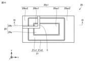
- Figure 10 is a schematic plan view showing the conductive portion 20 in the semiconductor device 100a according to the first embodiment.
- Figure 11 is a schematic cross-sectional view taken along line XI-XI in Figure 10.
- the insulating section 3 has an adhesive function for connecting the first conductive section 20a and the second conductive section 20b, and an electrical insulating function for insulating the first conductive section 20a and the second conductive section 20b.
- the material constituting the insulating section 3 is, for example, a thermosetting resin such as epoxy resin.
- a step (S2a) is performed in which the semiconductor substrate 1 is mounted on the conductive portion 20. Specifically, the electrode 11 formed on the first surface 1s1 of the semiconductor substrate 1 is connected to the conductive portion 20 via the joint 5.
- the step (S3a) of connecting the lead frames is carried out.
- the first wiring circuit 6a is connected to the first conductive portion 20a via the joint 5.
- the second wiring circuit 6b is connected to the second conductive portion 20b via the joint 5.
- the third wiring circuit 6c is connected to the upper electrode 11u of the semiconductor substrate 1 via the joint 5.
- the step (S4a) of forming the sealing resin 7 is carried out. Specifically, the support layer 40, the thermally conductive insulating layer 30, and the conductive portion 20 carrying the semiconductor substrate 1 described above are arranged in a metal mold for transfer molding. After that, the sealing resin 7 is formed by transfer molding.
- a semiconductor device 100a includes a semiconductor substrate 1 and a mounting substrate 2.
- the semiconductor substrate 1 has a first surface 1s1.
- the mounting substrate 2 has a main surface 20s1.
- the main surface 20s1 faces the first surface 1s1.
- An electric field intensity mitigating portion 12 and an electrode 11 are formed on the first surface 1s1.
- the electrode 11 is connected to the mounting substrate 2.
- a recess 21 is formed on the main surface 20s1.
- the recess 21 is disposed at a position overlapping the electric field intensity mitigating portion 12 in a plan view of the first surface 1s1.
- the recess 21 can be formed to sufficiently increase the distance between the electric field strength mitigation section 12 and the mounting substrate 2. This reduces the influence of the mounting substrate 2 on the electric field strength mitigation section 12. As a result, the voltage resistance of the semiconductor device 100a is improved.
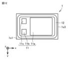
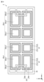
- FIG. 12 is a schematic bottom view of the semiconductor substrate 1 in the first modified example of the semiconductor device according to the first embodiment.
- FIG. 12 corresponds to FIG. 2.
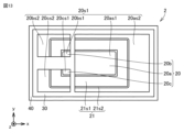
- FIG. 13 is a schematic plan view of the mounting substrate 2 in the first modified example of the semiconductor device 100a according to the first embodiment.
- FIG. 13 corresponds to FIG. 3.
- the semiconductor device 100a shown in FIG. 12 and FIG. 13 basically has the same configuration as the semiconductor device 100a shown in FIG. 1 to FIG. 6 and can obtain the same effect, but is different in that the third electrode 11c is formed on the first surface 1s1 of the semiconductor substrate 1 as shown in FIG. 12.
- at least one or more third electrodes 11c may be formed on the first surface 1s1.
- the number of the third electrodes 11c may be one or more.
- the third electrode 11c is disposed on the first surface 1s1 at a distance from the first electrode 11a and the second electrode 11b.
- the conductive portion 20 includes a third conductive portion 20c that can be wired in parallel to the second electrode 11b, which is the control electrode.
- the third conductive portion 20c is disposed at a distance from the first conductive portion 20a and the second conductive portion 20b.
- the first conductive portion 20a, the second conductive portion 20b, and the third conductive portion 20c only need to be insulated from one another. It is preferable that the spaces between the first conductive portion 20a, the second conductive portion 20b, and the third conductive portion 20c are filled with an insulating material such as silicone gel or epoxy resin.
- the insulating material filled between the first conductive portion 20a, the second conductive portion 20b, and the third conductive portion 20c may be, for example, the sealing resin 7 shown in FIG. 1.
- either the current sense line or the temperature sense line which is the wiring from the on-chip diode, may be connected to the third conductive portion 20c.
- the third electrode 11c has the same potential as the first electrode 11a.
- Fig. 14 is a schematic bottom view of the mounting substrate 2 in the modified example 2 of the semiconductor device 100a according to the first embodiment.
- Fig. 14 corresponds to Fig. 3.
- the mounting substrate 2 shown in Fig. 14 basically has the same configuration as the mounting substrate 2 in the semiconductor device 100a shown in Figs. 1 to 6, and can obtain the same effects, but is different in that the semiconductor device 100a according to the first embodiment has a plurality of semiconductor substrates 1, as shown in Fig. 14.
- the semiconductor device 100a shown in Figures 1 to 6 has one semiconductor substrate 1, but the semiconductor device 100a may have multiple semiconductor substrates 1.
- the semiconductor device 100a may have multiple semiconductor substrates 1 that are different from each other, or multiple semiconductor substrates 1 that have different structures from each other.
- the type of semiconductor substrate 1 has a structure called vertical type, there are no particular restrictions on the number of parallel substrates and combinations.
- the circuit configuration of the semiconductor device 100a is a so-called 2-in-1 type in which two semiconductor substrates 1 are mounted on one module.
- FIG. 14 shows a mounting substrate 2 that configures a half bridge. As shown in FIG. 14, the four first electrode side surfaces 20as1 arranged on both the left and right ends of the mounting substrate 2 may be connected to the semiconductor substrate 1 for the transistor. The four first electrode side surfaces 20as1 arranged in the center of the mounting substrate 2 may be connected to the semiconductor substrate 1 for the transistor.
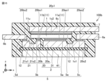
- FIG. 15 is a schematic cross-sectional view of a semiconductor device 100b according to a second embodiment.
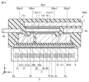
- FIG. 15 corresponds to FIG. 1.
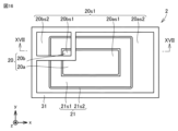
- FIG. 16 is a schematic plan view of a mounting substrate 2 in the semiconductor device 100b according to the second embodiment.
- FIG. 16 corresponds to FIG. 3.
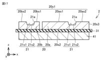
- FIG. 17 is a schematic cross-sectional view taken along line XVII-XVII in FIG. 16.
- FIG. 17 corresponds to FIG. 4.
- the semiconductor device 100b shown in FIGS. 15 to 17 basically has the same configuration as the semiconductor device 100a shown in FIGS. 1 and 6 and can achieve the same effects, but is different in that the member connected to the rear surface 20s2 of the conductive portion 20 is an insulating substrate 31, not a thermally conductive insulating layer 30.
- the mounting substrate 2 has a conductive portion 20, an insulating substrate 31, and a lower electrode 41.
- the insulating substrate 31 is connected to the rear surface 20s2 of the conductive portion 20.
- the lower electrode 41 is connected to the surface of the insulating substrate 31 opposite to the surface to which the conductive portion 20 is connected.
- the surface of the lower electrode 41 opposite to the surface to which the insulating substrate 31 is connected is exposed from the sealing resin 7.
- the material constituting the insulating substrate 31 may be any material, for example, a ceramic whose main component is either Si-N or Al-N.
- the insulating substrate 31 insulates the conductive portion 20 and the lower electrode 41.
- the lower electrode 41 has high thermal conductivity.
- the linear expansion coefficient of the lower electrode 41 is the same as the linear expansion coefficient of the conductive portion 20.
- the material constituting the lower electrode 41 is the same as the material constituting the conductive portion 20.
- the material constituting the lower electrode may include, for example, any one of aluminum (Al), an aluminum alloy, copper (Cu), and a copper alloy.
- the conductive portion 20, insulating substrate 31, and lower electrode 41 may each be joined by a direct joining method or an active metal brazing method.
- the direct joining method is a method in which two constituent materials are joined by a direct reaction.
- the active metal brazing method is a method in which two constituent materials are joined by a brazing material to which an active metal such as titanium or zirconium is added.
- the conductive portion 20, insulating substrate 31, and lower electrode 41 are integrated into the mounting substrate 2, which improves the handleability of the conductive portion 20 during the manufacturing process of the semiconductor device 100b.
- the mounting substrate 2 has an insulating substrate 31 and a lower electrode 41.
- the insulating substrate 31 is connected to the conductive portion 20.
- the lower electrode 41 is connected to the insulating substrate 31.
- the lower electrode 41 is disposed on the side of the insulating substrate 31 opposite to the side on which the conductive portion 20 is disposed.
- the conductive portion 20, the insulating substrate 31, and the lower electrode 41 are integrated into the mounting substrate 2.
- the handleability of the conductive portion 20 during the manufacturing process of the semiconductor device 100b is improved.
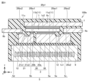
- Fig. 18 is a schematic cross-sectional view of a semiconductor device 100c according to a third embodiment.
- Fig. 18 corresponds to Fig. 1.
- the semiconductor device 100c shown in Fig. 18 basically has the same configuration as the semiconductor device 100a shown in Figs. 1 and 6, and can obtain the same effects, but is different in that a sealing resin 7 is formed by a case mold.
- a sealing resin 7 is formed by a case mold.
- a potting resin is used as the sealing resin 7.
- the material constituting the potting resin is, for example, a silicone gel.
- the case 8 is disposed on the support layer 40.
- the case 8 is disposed so as to surround the semiconductor substrate 1.
- the case 8 is fixed to the support layer 40 by adhesive or the like.
- the case 8 and the support layer 40 fixed by adhesive or the like are sealed.
- the material that constitutes the case 8 is preferably, for example, a material that can be injection molded and has high heat resistance and insulating properties. Any material may be used as the material that constitutes the case 8, but it may be, for example, an engineering plastic such as polyphenylene sulfide (PPS).
- PPS polyphenylene sulfide
- a step (S1c) of preparing a semiconductor substrate 1 and a mounting substrate 2 is performed.
- the mounting substrate 2 has a conductive portion 20, a thermally conductive insulating layer 30, and a support layer 40.
- a recess 21 is formed on the surface of the conductive portion 20.
- a step (S2c) is performed in which the semiconductor substrate 1 is mounted on the conductive portion 20. Specifically, the electrode 11 formed on the first surface 1s1 of the semiconductor substrate 1 is connected to the conductive portion 20 via the joint 5.
- the step (S3c) of connecting the lead frames is carried out.
- the first wiring circuit 6a is connected to the first conductive portion 20a via the joint 5.
- the second wiring circuit 6b is connected to the second conductive portion 20b via the joint 5.
- the third wiring circuit 6c is connected to the upper electrode 11u of the semiconductor substrate 1 via the joint 5.
- case 8 is fixed to support layer 40 with adhesive or the like. Then, case 8 is filled with potting resin or the like.
- a lid (not shown) may be mounted on the semiconductor device 100c.
- terminal processing such as bending may be performed on the wiring circuit extending outside the sealing resin 7.
- the semiconductor device 100c according to the third embodiment shown in FIG. 18 can be obtained.
- the semiconductor device 100c further includes a case 8.
- the case 8 surrounds the sealing resin 7.
- Fig. 19 is a schematic cross-sectional view of a semiconductor device 100d according to embodiment 4.
- Fig. 19 corresponds to Fig. 1.
- the semiconductor device 100d shown in Fig. 19 basically has a similar configuration to the semiconductor device 100a shown in Fig. 1 to Fig. 6 and can obtain similar effects, but differs in that it includes a cooler 9.
- the cooler 9 is connected to the back surface of the support layer 40 exposed from the sealing resin 7 via the sixth joint 5f.
- a flow path is formed inside the cooler 9 for circulating a liquid as a refrigerant.
- the cooler 9 in the semiconductor device 100d according to the fourth embodiment is a cooler 9 for liquid cooling, but may also be a cooler 9 for air cooling. In this way, the heat dissipation properties of the semiconductor device 100d are improved.
- the sixth joint 5f can be made of solder, but it is particularly preferable to use a material that has high thermal conductivity and can ensure long-term reliability even when the joint is thin.
- the material constituting the cooler 9 may be any material having high thermal conductivity.
- the material constituting the cooler 9 may include, for example, aluminum (Al), an aluminum alloy, copper (Cu), or a copper alloy.
- the sealing resin 7 when the sealing resin 7 is formed by case molding, it is preferable to fill the case 8 with potting resin after bonding the cooler 9 to the mounting substrate 2.
- the semiconductor device 100d further includes a cooler 9.
- the cooler 9 is connected to the mounting board 2.
- Fig. 20 is a schematic cross-sectional view of a semiconductor device 100e according to embodiment 5.
- Fig. 20 corresponds to Fig. 1.
- the semiconductor device 100e shown in Fig. 20 basically has the same configuration as the semiconductor device 100a shown in Fig. 1 to Fig. 6 and can obtain the same effects, but differs in that the sealing resin 7 seals a part of the cooler 9.
- the cooler 9 plays the role of the support layer 40 of the mounting substrate 2. Therefore, the thermally conductive insulating layer 30 is connected to the cooler 9. Therefore, the cooler 9 does not have to be connected to the thermally conductive insulating layer 30 via the sixth joint 5f shown in FIG. 19. In this way, the heat dissipation properties of the semiconductor device 100e are further improved.
- FIG. 21 is a schematic cross-sectional view of a modified example of the semiconductor device 100e according to the fifth embodiment.
- FIG. 21 corresponds to FIG. 1.
- the semiconductor device 100e shown in FIG. 21 basically has the same configuration as the semiconductor device 100e shown in FIG. 20 and can achieve the same effects, but differs in that the sealing resin 7 seals the entire cooler 9.
- the semiconductor device 100e has at least a part of the cooler 9 sealed therein.
Landscapes
- Structures Or Materials For Encapsulating Or Coating Semiconductor Devices Or Solid State Devices (AREA)
Abstract
半導体装置(100a)は、半導体基板(1)と実装基板(2)とを備える。半導体基板(1)は第1面(1s1)を有する。実装基板(2)は主面(20s1)を有する。主面(20s1)は第1面(1s1)に対面する。第1面(1s1)には、電界強度緩和部(12)と、電極(11)とが形成されている。電極(11)は、実装基板(2)に接続されている。主面(20s1)には、凹部(21)が形成されている。凹部(21)は、第1面(1s1)の平面視において電界強度緩和部(12)に重なる位置に配置されている。
Description
本開示は、半導体装置に関する。
従来、半導体基板の裏面と実装基板とが対向するように当該実装基板が半導体基板の電極に接続されているフリップチップ実装が用いられた半導体装置が知られている(例えば、特開2013‐89948号公報参照)。特開2013‐89948号公報では、半導体基板は活性領域に発生する高電界を緩和する電界強度緩和部としてガードリングを有する。
しかし、上記のような半導体装置において、実装基板およびガードリングが近接すると、半導体基板における活性領域の電界が緩和されず、半導体装置の耐圧性が悪化する。
本開示は、上記のような課題を解決するために成されたものであり、本開示の目的は、耐圧性が改善された半導体装置を提供することである。
本開示に従った半導体装置は、半導体基板と実装基板とを備える。半導体基板は第1面を有する。実装基板は主面を有する。主面は第1面に対面する。第1面には、電界強度緩和部と、電極とが形成されている。電極は、実装基板に接続されている。主面には、凹部が形成されている。凹部は、第1面の平面視において電界強度緩和部に重なる位置に配置されている。
上記によれば、耐圧性が改善された半導体装置を得ることができる。
以下、本開示の実施の形態を説明する。なお、特に言及しない限り、以下の図面において同一または対応する部分には同一の参照番号を付し、その説明は繰り返さない。
実施の形態1.
<半導体装置の構成>
図1は、実施の形態1に係る半導体装置100aの概略断面図である。図2は、実施の形態1に係る半導体装置100aにおける半導体基板1の概略底面図である。図3は、実施の形態1に係る半導体装置100aにおける実装基板2の概略平面図である。図4は、図3の線分IV-IVにおける概略断面図である。図5は、図3の線分V-Vにおける概略断面図である。図6は、実施の形態1に係る半導体装置100aにおける電界強度緩和部12および凹部21の概略部分断面図である。
<半導体装置の構成>
図1は、実施の形態1に係る半導体装置100aの概略断面図である。図2は、実施の形態1に係る半導体装置100aにおける半導体基板1の概略底面図である。図3は、実施の形態1に係る半導体装置100aにおける実装基板2の概略平面図である。図4は、図3の線分IV-IVにおける概略断面図である。図5は、図3の線分V-Vにおける概略断面図である。図6は、実施の形態1に係る半導体装置100aにおける電界強度緩和部12および凹部21の概略部分断面図である。
図1から図6に示された半導体装置100aは、たとえば、電力用の半導体装置100aであって、半導体基板1と、実装基板2と、接合部5と、配線回路6と、封止樹脂7とを主に備える。接合部5は、第1接合部5a、第2接合部5b、第3接合部5c、第4接合部5d、および第5接合部5eを含む。配線回路6は、第1配線回路6a、第2配線回路6b、および第3配線回路6cを含む。
半導体基板1は、第1面1s1と第2面1s2と第3面1s3とを有する。第1面1s1は、実装基板2の主面20s1に対向する面である。第2面1s2は、第1面1s1の反対側の面である。第3面1s3は、第1面1s1と第2面1s2とを接続する。本実施の形態1に係る半導体装置100aにおいて、第1面1s1は、半導体基板1の裏面である。本実施の形態1に係る半導体装置100aにおいて、第2面1s2は、半導体基板1の表面である。本実施の形態1に係る半導体装置100aにおいて、第3面1s3は、半導体基板1の側面である。
第1面1s1および第2面1s2は、x方向と、x方向に垂直なy方向とに延在している。x方向は、配線回路が延びている方向である。y方向は、x方向に対して垂直な方向である。z方向は、半導体基板1の厚さ方向である。第1面1s1の法線方向は、z方向方向である。第2面1s2は+z方向を向いている。第1面1s1は、-z方向を向いている。
図1および図2に示されているように、第1面1s1には、電界強度緩和部12と、電極11とが形成されている。電界強度緩和部12は、半導体基板1の裏面上に形成される電界強度を緩和する。そのため、電界強度緩和部12は、第1面1s1上において電極11に対して離間して配置されている。図2に示されているように、電界強度緩和部12は、電極11を囲むように配置されていてもよい。電界強度緩和部12の形状は、たとえば、環状であってもよい。具体的には、電界強度緩和部12は、ガードリングと呼ばれる終端構造であってもよい。
電界強度緩和部12の形状は、環状でなくてもよい。具体的には、電界強度緩和部12は、JTE(Junction Termination Extension)構造と呼ばれる終端構造であってもよい。電界強度緩和部12は、たとえば、p型領域であって、イオン注入によって形成されてもよい。
図2に示されているように、電極11は、第1電極11aと、第2電極11bとを含む。第1電極11aは、主電極である。主電極には主電流が流れる。第2電極11bは、制御電極である。制御電極は、主電流を制御する。第1電極11aおよび第2電極11bは第1面1s1上において互いに離間して配置されている。
第1電極11aは、第1接合部5aを介して実装基板2に接続されている。第2電極11bは、第2接合部5bを介して実装基板2に接続されている。
図1に示されているように、半導体基板1の第2面1s2には、上電極11uが形成されている。上電極11uには主電流が流れる。上電極11uには、第5接合部5eを介して第3配線回路6cが接続されている。第3配線回路6cは、x方向に延びている。
半導体基板1は、電力を制御するいわゆる電力用の半導体基板1である。半導体基板1を構成する材料として、任意の材料を用いてもよい。半導体基板1を構成する材料として、珪素(Si)、炭化珪素(SiC)、窒化ガリウム(GaN)、酸化ガリウム(GaO)といった材料を用いてもよい。
半導体基板1に形成されている半導体素子の種類としては、特に限定する必要はないが、たとえば縦型の半導体素子であってもよい。この場合、当該半導体基板1のz方向(厚さ方向)に主電流が流れる。本実施の形態1における半導体基板1は、制御電極を有するトランジスタであるが、縦型の半導体素子であればダイオードであってもよく、他の機能を有してもよい。半導体基板1は、たとえばIGBT(Insulated Gate Bipolar Transistor)、MOSFET(Metal Oxide Semiconductor Field Effect Transistor)等を用いることができる。
電極11を構成する材料は、高い導電性および熱伝導性を有する材料であることが好ましい。電極11を構成する材料は、たとえば、アルミニウム(Al)、アルミニウム合金、銅(Cu)、銅合金のいずれかを含んでもよい。電極11は、Al/Cuの2層構造であってもよく、金(Au)および銀(Ag)のいずれかを含む多層構造であってもよい。
電極11は、拡散防止層を含んでもよい。拡散防止層として、たとえば、チタン(Ti)等を含んでもよい。半導体基板1とオーミックコンタクトをとるために、電極11の下地層としてニッケル(Ni)シリサイドを用いてもよい。電極11の酸化防止あるいは接合性向上のために、電極11は薄い表面層を含んでもよい。表面層を構成する材料は、たとえば金などの貴金属である。
本実施の形態1に係る半導体装置100aにおいて、電極11に特段の制約はない。たとえば、第1電極11aおよび第2電極11bの配置箇所に特段の制約はない。具体的には、図2に示されているように、制御電極として第2電極11bは第1面1s1上の隅に配置されてもよいが、第1面1s1の中心に配置されてもよい。
第2電極11bの形状は、任意の形状であってもよい。第2電極11bの形状は、たとえば、図2に示されているように四角形状であってもよく、その他に、円状であってもよく、楕円状であってもよく、楕円状と四角状とを組み合わせた形状であってもよい。第2電極11bの形状は、六角形状であってもよい。
図1に示されているように、実装基板2は、導電部20と、熱伝導性絶縁層30と、支持層40とを有している。導電部20は、表面と裏面20s2と側面20s3とを有する。表面は、半導体基板1の第1面1s1に対面している。つまり、実装基板2の主面20s1は、導電部20の表面から構成される。裏面20s2は、導電部20の表面の反対側の面である。側面20s3は、表面と裏面20s2とを接続する面である。
図1に示されているように、熱伝導性絶縁層30は、導電部20の裏面20s2に接続されている。支持層40は、熱伝導性絶縁層30において導電部20が接続されている面の反対側の面に接続されている。支持層40において、熱伝導性絶縁層30が接続されている面の反対側の面が封止樹脂7から露出している。
導電部20は、第1導電部20aと第2導電部20bとを含む。第1導電部20aは、第2導電部20bに対して離間して配置されている。第1導電部20aおよび第2導電部20bは互いに絶縁されていればよい。図1に示されているように、第1導電部20aと第2導電部20bとの間は、たとえば、シリコーンゲルあるいはエポキシ樹脂などの絶縁材料で充填されていることが好ましい。本実施の形態1に係る半導体装置100aにおいて、第1導電部20aと第2導電部20bとの間に充填される絶縁材料として、たとえば、図1に示されているように、封止樹脂7であってもよい。
当該半導体装置100aの製造工程において、任意の段階で、第1導電部20aと第2導電部20bとの間に、絶縁材料が充填されてもよい。たとえば、半導体装置100aの製造工程の初期段階で、第1導電部20aと第2導電部20bとの間に、絶縁材料が充填されてもよい。たとえば、当該半導体装置100aの製造工程において最終工程に近い段階で、第1導電部20aと第2導電部20bとの間に、絶縁材料が充填されてもよい。
耐熱性の観点から、第1導電部20aと第2導電部20bとの間に充填される絶縁材料がシリコーンゲルである場合、半導体装置100aが高温で処理される工程を経た後に、当該絶縁材料を充填することが好ましい。
図3に示されているように、実装基板2の主面20s1には凹部21が形成されている。つまり、凹部21は、導電部20の表面に形成されている。第1導電部20aにおいて、主面20s1は、第1電極側面20as1と、第1配線回路側面20as2とを含む。第1電極側面20as1および第1配線回路側面20as2の間に凹部21が形成されている。凹部21には、封止樹脂7が充填されていることが好ましい。
第2導電部20bにおいて、主面20s1は、第2電極側面20bs1と、第2配線回路側面20bs2とを含む。第2電極側面20bs1および第2配線回路側面20bs2の間に凹部21が形成されている。
導電部20は、電極11に接続されている。具体的には、第1電極11aは、第1導電部20aの第1電極側面20as1に第1接合部5aを介して接続されている。第2電極11bは、第2導電部20bの第2電極側面20bs1に第2接合部5bを介して接続されている。
つまり、z方向からみた平面視において、第1電極11aは、第1導電部20aの第1電極側面20as1に重なる位置に配置されている。z方向からみた平面視において、第2電極11bは、第2導電部20bの第2電極側面20bs1に重なる位置に配置されている。
図1に示されているように、第1配線回路6aは、第1配線回路側面20as2に第3接合部5cを介して接続されている。第1配線回路6aは、x方向に延びている。第2配線回路6bは、第2配線回路側面20bs2に第4接合部5dを介して接続されている。第2配線回路6bは、-x方向に延びている。このようにして、主電極である第1電極11aと第1導電部20aとが電気的および機械的に接続され、制御電極である第2電極11bと第2導電部20bとが電気的および機械的に接続される。
導電部20を構成する材料は、高い導電性および熱伝導性を有する材料であることが好ましい。導電部20を構成する材料は、たとえば、アルミニウム(Al)、アルミニウム合金、銅(Cu)、銅合金のいずれかを含んでもよい。
熱伝導性絶縁層30は、接着機能、電気的絶縁機能、熱伝導機能を有する材料であることが好ましい。熱伝導性絶縁層30を構成する材料は、たとえば、無機充填材を含有した熱硬化性樹脂シート、熱硬化性樹脂が含侵された無機成形体シート、および塗布膜などであってもよい。熱伝導性絶縁層30は、互いに離間している第1導電部20aおよび第2導電部20bとを固定する。
支持層40の下面に冷却器(図示せず)が接続されてもよい。支持層40は、当該冷却器に熱を伝えることができる材料であってもよい。具体的は、支持層40を構成する材料は、高い熱伝導率を有する銅、アルミニウム、あるいはそれらの合金を含む金属薄板あるいは金属箔であってもよい。また、支持層40は、当該半導体装置100aの機械的強度の大半を占める。そのため、支持層40は高い機械的強度を有することが好ましい。
実装基板2において、導電部20、熱伝導性絶縁層30、および支持層40は熱伝導性絶縁層30の接着機能により接着されている。具体的には、加圧および加温することで導電部20、熱伝導性絶縁層30、および支持層40が接着される。
第1配線回路6a、第2配線回路6b、第3配線回路6cを構成する部材は、たとえば導電性を有するリードフレームであってもよい。第1配線回路6a、第2配線回路6b、第3配線回路6cは、主面20s1に対して平行となるように配置されていることが好ましい。特に、第1配線回路6aおよび第3配線回路6cの形状は、平板状であることが好ましい。このようにすれば、寄生インダクタンスが低減される。
封止樹脂7は、半導体基板1と、実装基板2と、第1配線回路6aの一部と、第2配線回路6bの一部と、第3配線回路6cの一部とを覆う。このようにすれば、半導体装置100aの絶縁性が向上し、湿度や汚染などによる外部環境の影響を低減できる。
第1配線回路6aは第1導電部20aの第1配線回路側面20as2から封止樹脂7の外側へ延在している。第2配線回路6bは第2導電部20bの第2配線回路側面20bs2から封止樹脂7の外側へ延在している。第3配線回路6cは半導体基板1の第2面1s2から封止樹脂7の外側へ延在している。
封止樹脂7の外部において外部機器と接続できるように、第1配線回路6a、第2配線回路6b、第3配線回路6cの各々における一部は、封止樹脂7の表面から外側へ延在している。第1配線回路6a、第2配線回路6b、第3配線回路6cは、封止樹脂7の外側に延在している部分において、たとえばフォーミングにより屈曲していてもよい。
接合部5を構成する材料として、はんだが挙げられる。ただし、はんだは比較的高い熱抵抗を有するため、本実施の形態1に係る半導体装置100aの接合部5を構成する材料としてはんだ以外の材料を用いてもよい。また、接合部5の長期信頼性の観点からも、はんだ以外の材料を用いてもよい。なお、熱抵抗は、熱伝導率と、z方向における接合厚さと、x方向およびy方向における接合部5の断面積とから決定される。
特に、はんだを用いて第3接合部5c、第4接合部5d、第5接合部5eを形成すると、当該半導体装置100aの製造工程上、プロセス温度、温度プロファイルによって、はんだの再溶融が発生し得る。そのため、本実施の形態1に係る半導体装置100aの第3接合部5c、第4接合部5d、第5接合部5eを構成する材料としてはんだとは異なる材料を用いてもよい。
たとえば、銀(Ag)あるいは銅(Cu)等の微粒子を含む焼結材は、本実施の形態1に係る半導体装置100aの接合部5を構成する材料として好ましい。焼結材を用いて接合部5を形成することで、接合厚さが薄くなる。また、焼結材は、高い熱伝導率を有する。その結果、当該接合部5は小さい熱抵抗を有する。接合部5を形成する際に、加圧、無加圧、プロセス温度、温度プロファイルについて、特段条件はない。
Cu-Sn等の液相拡散によって接合部5が形成されてもよい。このようにすれば、接合厚さを低減するため、当該接合部5における熱抵抗を更に低減することができる。
熱抵抗の更なる抑制のために、接合部5は形成されてなくてもよい。固相反応によって、半導体装置100aを構成する部材が直接的に接合されてもよい。具体的には、第1電極11aおよび第1導電部20aが、第1接合部5aを介さず、固相反応により直接的に接続されてもよい。
当該半導体装置100aの動作時に、半導体基板1は発熱する。半導体基板1で発生した熱は、電極11を通過する。制御電極である第2電極11bを通過する熱量は、主電極である第1電極11aを通過する熱量より小さい。そのため、第1接合部5aおよび第2接合部5bを形成する際、第1接合部5aおよび第2接合部5bは同じ材料でなくてもよい。ただし、製造工程の短縮の観点から、第1接合部5aおよび第2接合部5bは同じ材料であることが好ましい。
製造工程の短縮の観点から、第3接合部5c、第4接合部5d、第5接合部5eを構成する材料は、第1接合部5a、第2接合部5bと同じ材料であってもよい。第3接合部5c、第4接合部5d、第5接合部5eを形成せず、超音波接合あるいはレーザー溶接によって直接的にリードフレームを接合してもよい。
封止樹脂7を構成する材料は、たとえば、エポキシ樹脂などの熱硬化性樹脂であってもよい。封止樹脂7は、たとえば、トランスファーモールドによって形成される。後述するように、封止樹脂7は、ケースモールドによって形成されてもよい。
ここで、本実施の形態1に係る半導体装置100aの特徴は、図1および図3に示されるように、実装基板2の主面20s1に凹部21が形成されている点である。凹部21は、第1面1s1の平面視において、電界強度緩和部12に重なる位置に配置されている。
前述したように、電界強度緩和部12は、半導体基板1の裏面上に形成される電界強度を緩和する。ただし、実装基板2が当該電界強度緩和部12の近傍に配置されている場合、実装基板2が電界強度緩和部12の電界強度に影響を与えてしまう。その結果、半導体装置100aの耐圧性が悪化するおそれがある。
本実施の形態1に係る半導体装置100aにおいて、実装基板2の主面20s1に凹部21が形成されていることで、電界強度緩和部12が実装基板2から受ける影響が抑制される。その結果、半導体装置100aの耐圧性が改善する。
図3に示されているように、凹部21は電界強度緩和部12の形状に沿って形成されていることが好ましい。具体的には、主面20s1の平面視において凹部21の形状は、環状であってもよい。
このようにすることで、電界強度緩和部12が実装基板2から受ける影響が抑制される。また、半導体基板1の裏面(第1面1s1)が、放熱面として熱抵抗が抑制される。その結果、当該半導体装置100aの放熱性が向上する。
図4および図5に示されているように、凹部21は、底面21s1と側面21s2とを有する。底面21s1は、凹部21において、第1面1s1および電界強度緩和部12からz方向において最も離れた面である。側面21s2は、主面20s1と底面21s1とを接続する面である。
図4および図5に示されているように、主面20s1から底面21s1までの距離t1は、導電部20の厚みt2より小さい。導電部20の厚みt2は、導電部20の表面から裏面20s2までのz方向における距離である。つまり、凹部21の内周面は導電体により構成されており、当該内周面は電気的に連続している。異なる観点から言うと、たとえば、第1導電部20aにおいて第1電極側面20as1および第1配線回路側面20as2は凹部21を介して導通している。第2導電部20bにおいて第2電極側面20bs1および第2配線回路側面20bs2は凹部21を介して導通している。
凹部21は、主面20s1上に形成された開口部21aを有する。図4および図5に示されているように、z方向に沿った断面において、凹部21の形状は、開口部21aから底面21s1に向かって狭くなっている形状であってもよい。具体的には、図4に示されているように、底面21s1の幅w1は開口部21aの幅w2より小さい。このようにすることで、半導体基板1で発生し電極11を通過する熱の流路幅が広がり、当該半導体装置100aにおける熱抵抗が低減する。
図6に示されているように、z方向に沿った断面において、側面21s2の形状は、直線的なテーパ状であってもよい。具体的には、z方向に沿った断面において、側面21s2の形状は、直線部Lを有してもよい。後述するように、z方向に沿った断面において、側面21s2は、円弧状あるいは楕円状であってもよい。具体的には、z方向に沿った断面において、側面21s2は、曲線部Rを有してもよい。
側面21s2は、直線部Lおよび曲線部Rを組み合わせた面であってもよい。このようにして、z方向における断面において、凹部21の形状は、開口部21aから底面21s1に向かって狭くなっている形状であってもよい。
図6に示されているように、凹部21の幅w1は、電界強度緩和部12の幅dより大きいことが好ましい。凹部21の幅w1は、第3面1s3から電界強度緩和部12の内周面までの距離lより大きいことがより好ましい。
図7から図9は、実施の形態1に係る半導体装置100aにおける凹部21の変形例における概略部分断面図である。図7から図9は、図6に対応する。図7から図9に示された半導体装置100aは、基本的には図1から図6に示された半導体装置100aと同様の構成を備え、同様の効果を得ることができるが、凹部21の形状が異なる。
図7に示されているように、底面21s1が実装基板2の側面20s3にまで延在していてもよい。図7に示されているように、凹部21の幅w1は、凹部21の側面21s2から実装基板2の側面20s3までのx方向における距離である。
なお、第1配線回路6a、第2配線回路6bなどのリードフレームは、凹部21の底面21s1に接続されてもよい。ただし、凹部21の底面21s1より、第1配線回路側面20as2および第2配線回路側面20bs2などの主面20s1の表面モフォロジーが優れている。そのため、第1配線回路6a、第2配線回路6bなどのリードフレームは、第1配線回路側面20as2および第2配線回路側面20bs2などの主面20s1に接続されていることが好ましい。
図8に示されているように、z方向に沿った断面において、側面21s2は、曲線部Rを有してもよい。側面21s2は、直線部Lと曲線部Rとを組み合わせた面であってもよい。
凹部21において、内周側の側面21s2および外周側の側面21s2の形状が互いに異なっていてもよい。具体的には、図9に示されているように、内周側の側面21s2の断面形状が円弧状あるいは楕円状などの曲線状であり、外周側の側面21s2の断面形状が直線状であってもよい。また、外周側の側面21s2はテーパ状に底面21s1に対して傾斜していてもよい。具体的には、内周側の側面21s2は、曲線部Rを有しており、外周側の側面21s2が、直線部Lを有していてもよい。このようにすることで、z方向における断面において、凹部21の形状は、開口部21aから底面21s1に向かって狭くなっている形状であってもよい。
上述のような凹部21は、シリコーンゲルあるいはエポキシ樹脂などの絶縁材料で充填されていることが好ましい。本実施の形態1に係る半導体装置100aにおいて、凹部21に充填される絶縁材料として、たとえば、図1に示されているように、封止樹脂7であってもよい。
凹部21は、機械加工あるいは化学加工などの任意の方法で形成されてもよい。機械加工として、具体的には、切削加工、研削加工、フライス加工等の除去加工、およびプレス加工、鋳造加工、鍛造加工等の成形加工などが挙げられる。化学加工として、具体的には、エッチング加工などが挙げられる。
<半導体装置の製造方法>
本実施の形態に係る半導体装置100aの製造方法では、まず半導体基板1および導電部20を準備する工程(S1a)を実施する。導電部20の表面上には凹部21が形成されている。導電部20は、第1導電部20aおよび第2導電部20bを含む。第1導電部20aおよび第2導電部20bは、互いに離間して配置される。
本実施の形態に係る半導体装置100aの製造方法では、まず半導体基板1および導電部20を準備する工程(S1a)を実施する。導電部20の表面上には凹部21が形成されている。導電部20は、第1導電部20aおよび第2導電部20bを含む。第1導電部20aおよび第2導電部20bは、互いに離間して配置される。
第1導電部20aおよび第2導電部20bが互いに離れている状態だと、当該半導体装置100aの製造工程中において、当該導電部20の取り扱いが困難となる。そのため、図10および図11に示されているように、第1導電部20aおよび第2導電部20bは、絶縁材料として絶縁部3を介して接続されていてもよい。図10は、実施の形態1に係る半導体装置100aにおける導電部20を示す概略平面図である。図11は、図10の線分XI-XIにおける概略断面図である。
絶縁部3は、第1導電部20aおよび第2導電部20bを接続する接着機能と、第1導電部20aおよび第2導電部20bを絶縁する電気的絶縁機能とを有する。絶縁部3を構成する材料は、たとえば、エポキシ樹脂などの熱硬化性樹脂である。このように、絶縁部3を用いることで、当該半導体装置100aの製造工程中に第1導電部20aおよび第2導電部20bを一体として取り扱うことができる。また、第1導電部20aおよび第2導電部20bが一体となっているため、導電部20における機械的強度が確保される。
次に、導電部20に半導体基板1を搭載する工程(S2a)を実施する。具体的には、半導体基板1の第1面1s1に形成された電極11と導電部20とを接合部5を介して接続する。
次に、リードフレームを接続する工程(S3a)を実施する。具体的には、第1導電部20aに接合部5を介して第1配線回路6aを接続する。第2導電部20bに接合部5を介して第2配線回路6bを接続する。半導体基板1の上電極11uに接合部5を介して第3配線回路6cを接続する。
次に、封止樹脂7を形成する工程(S4a)を実施する。具体的には、トランスファーモールド用の金型内に、支持層40、熱伝導性絶縁層30、および上述した半導体基板1を搭載した導電部20を配置する。その後、トランスファーモールドによって封止樹脂7を形成する。
このようにして、図1から図6に示された本実施の形態1に係る半導体装置100aを得ることができる。
<半導体装置の製造方法の変形例>
本実施の形態1に係る半導体装置100aの製造方法の変形例では、まず半導体基板1および実装基板2を準備する工程(S1b)を実施する。実装基板2は、導電部20、熱伝導性絶縁層30、および支持層40を有する。導電部20の表面上には凹部21が形成されている。
本実施の形態1に係る半導体装置100aの製造方法の変形例では、まず半導体基板1および実装基板2を準備する工程(S1b)を実施する。実装基板2は、導電部20、熱伝導性絶縁層30、および支持層40を有する。導電部20の表面上には凹部21が形成されている。
このようにすることで、当該半導体装置100aの製造工程中に、導電部20、熱伝導性絶縁層30、および支持層40が実装基板2として一体となっていることで、導電部20における機械的な強度が確保される。また、導電部20、熱伝導性絶縁層30、および支持層40が実装基板2として一体となっていることで、当該半導体装置100aの製造工程における導電部20の取り扱い性が向上する。そのため、半導体装置100aの製造工程において、導電部20、熱伝導性絶縁層30、および支持層40が実装基板2として一体となって製造されることが好ましい。
次に、導電部20に半導体基板1を搭載する工程(S2b)を実施する。具体的には、半導体基板1の第1面1s1に形成された電極11と導電部20とを接合部5を介して接続する。
次に、リードフレームを接続する工程(S3b)を実施する。具体的には、第1導電部20aに接合部5を介して第1配線回路6aを接続する。第2導電部20bに接合部5を介して第2配線回路6bを接続する。半導体基板1の上電極11uに接合部5を介して第3配線回路6cを接続する。
次に、封止樹脂7を形成する工程(S4b)を実施する。具体的には、トランスファーモールド用の金型内に、半導体基板1を搭載した実装基板2を配置する。その後、トランスファーモールドによって封止樹脂7を形成する。
この工程(S4b)において、樹脂による圧力を利用して、熱伝導性絶縁層30の接着機能、電気的絶縁機能を発生させる必要がない。そのため、この工程(S4b)におけるトランスファーモールドによって封止樹脂7を形成する際の条件が緩和する。
このようにして、図1から図6に示された本実施の形態1に係る半導体装置100aを得ることができる。
<作用効果>
本開示に従った半導体装置100aは、半導体基板1と実装基板2とを備える。半導体基板1は第1面1s1を有する。実装基板2は主面20s1を有する。主面20s1は第1面1s1に対面する。第1面1s1には、電界強度緩和部12と、電極11とが形成されている。電極11は、実装基板2に接続されている。主面20s1には、凹部21が形成されている。凹部21は、第1面1s1の平面視において電界強度緩和部12に重なる位置に配置されている。
本開示に従った半導体装置100aは、半導体基板1と実装基板2とを備える。半導体基板1は第1面1s1を有する。実装基板2は主面20s1を有する。主面20s1は第1面1s1に対面する。第1面1s1には、電界強度緩和部12と、電極11とが形成されている。電極11は、実装基板2に接続されている。主面20s1には、凹部21が形成されている。凹部21は、第1面1s1の平面視において電界強度緩和部12に重なる位置に配置されている。
このようにすることで、凹部21が形成されることで電界強度緩和部12と実装基板2との間の距離を充分大きくできる。このため、電界強度緩和部12が実装基板2から受ける影響が抑制される。その結果、半導体装置100aの耐圧性が改善する。
上記半導体装置100aにおいて、第1面1s1に対して垂直な方向をz方向とする。凹部21は、開口部21aと底面21s1とを有する。開口部21aは、主面20s1上に形成されている。底面21s1は、第1面1s1からz方向において最も離れている。底面21s1の幅w1は開口部21aの幅w2よりも小さい。
このようにすれば、半導体基板1で発生し電極11を通過する熱の流路幅が広がり、当該半導体装置100aにおける熱抵抗が低減する。
上記半導体装置100aにおいて、凹部21は、側面21s2を有する。側面21s2は、主面20s1と底面21s1とを接続する。z方向に沿った断面において、側面21s2は直線部Lを有する。
このようにすれば、z方向における断面において、凹部21の形状は、開口部21aから底面21s1に向かって狭くなっている形状となる。その結果、半導体基板1で発生し電極11を通過する熱の流路幅が広がり、当該半導体装置100aにおける熱抵抗が低減する。
上記半導体装置100aにおいて凹部21は、凹部21は、側面21s2を有する。側面21s2は、主面20s1と底面21s1とを接続する。z方向に沿った断面において、側面21s2は曲線部Rを有する。
このようにすれば、z方向における断面において、凹部21の形状は、開口部21aから底面21s1に向かって狭くなっている形状となる。その結果、半導体基板1で発生し電極11を通過する熱の流路幅が広がり、当該半導体装置100aにおける熱抵抗が低減する。
上記半導体装置100aにおいて、電極11は、第1電極11aと第2電極11bとを含む。第1電極11aは、主電極である。第2電極11bは、制御電極である。実装基板2は、導電部20を有する。導電部20は、第1導電部20aと、第2導電部20bとを含む。第1導電部20aは、第1電極11aに接続されている。第2導電部20bは、第2電極11bに接続されている。第1導電部20aおよび第2導電部20bは、絶縁部を介して接続されている。
このようにすれば、半導体装置100aの製造工程中に第1導電部20aおよび第2導電部20bを一体として取り扱うことができる。つまり、半導体装置100aの製造工程における導電部20の取り扱い性が向上する。また、第1導電部20aおよび第2導電部20bが一体となっているため、導電部20における機械的強度が確保される。
上記半導体装置100aにおいて、実装基板2は、熱伝導性絶縁層30を有する。熱伝導性絶縁層30は、導電部20に接続されている。
このようにすれば、導電部20における機械的な強度が確保される。また、導電部20、熱伝導性絶縁層30、および支持層40が実装基板2として一体となっていることで、当該半導体装置100aの製造工程における導電部20の取り扱い性が向上する。
<変形例1の構成>
図12は、実施の形態1に係る半導体装置の変形例1における半導体基板1の概略底面図である。図12は、図2に対応する。図13は、実施の形態1に係る半導体装置100aの変形例1における実装基板2の概略平面図である。図13は、図3に対応する。図12および図13に示された半導体装置100aは、基本的には図1から図6に示された半導体装置100aと同様の構成を備え、同様の効果を得ることができるが、図12に示されているように、半導体基板1の第1面1s1に第3電極11cが形成されている点で異なる。第1電極11aおよび第2電極11bの他に、第1面1s1に少なくとも1以上の第3電極11cが形成されていてもよい。第3電極11cの数は、1であってもよく、複数であってもよい。
図12は、実施の形態1に係る半導体装置の変形例1における半導体基板1の概略底面図である。図12は、図2に対応する。図13は、実施の形態1に係る半導体装置100aの変形例1における実装基板2の概略平面図である。図13は、図3に対応する。図12および図13に示された半導体装置100aは、基本的には図1から図6に示された半導体装置100aと同様の構成を備え、同様の効果を得ることができるが、図12に示されているように、半導体基板1の第1面1s1に第3電極11cが形成されている点で異なる。第1電極11aおよび第2電極11bの他に、第1面1s1に少なくとも1以上の第3電極11cが形成されていてもよい。第3電極11cの数は、1であってもよく、複数であってもよい。
図12に示されているように、第3電極11cは、第1面1s1上において第1電極11aおよび第2電極11bに対して離間して配置されている。このようにすれば、第3電極11cが、主電極である第1電極11aと同電位である時、導電部20は制御電極である第2電極11bに対して平行に配線が可能な第3導電部20cを含む。その結果、耐ノイズ性が向上した半導体装置100aを得ることができる。
前述したように、第1面1s1に第3電極11cが形成されている時、図13に示されているように、導電部20は第3導電部20cを更に含む。第3導電部20cは接合部5(図示せず)を介して第3電極11cに接続されている。
図13に示されているように、第3導電部20cは、第1導電部20aおよび第2導電部20bに対して離間して配置されている。第1導電部20a、第2導電部20b、および第3導電部20cは互いに絶縁されていればよい。第1導電部20a、第2導電部20b、および第3導電部20cの間は、たとえば、シリコーンゲルあるいはエポキシ樹脂などの絶縁材料で充填されていることが好ましい。第1導電部20a、第2導電部20b、および第3導電部20cの間に充填される絶縁材料として、たとえば、図1に示されている封止樹脂7であってもよい。
第3導電部20cにおいて、主面20s1は、第3電極側面20cs1と、第3配線回路側面20cs2とを含む。第3電極側面20cs1および第3配線回路側面20cs2の間に凹部21が形成されている。
z方向からみた平面視において、第3電極11cは、第3導電部20cの第3電極側面20cs1に重なる位置に配置されている。第3配線回路側面20cs2に、電流センス線およびオンチップダイオードからの配線である温度センス線のいずれかが接続されていてもよい。このようにして、第3電極11cと第3導電部20cとが電気的および機械的に接続されてもよい。
<作用効果>
上記半導体装置100aにおいて、電極11は、少なくとも1以上の第3電極11cを含む。導電部20は、第3導電部20cを含む。第3導電部20cは、第3電極11cに接続されている。
上記半導体装置100aにおいて、電極11は、少なくとも1以上の第3電極11cを含む。導電部20は、第3導電部20cを含む。第3導電部20cは、第3電極11cに接続されている。
このようにすることで、第3導電部20cに、電流センス線およびオンチップダイオードからの配線である温度センス線のいずれかが接続されていてもよい。
上記半導体装置100aにおいて、第3電極11cは、第1電極11aと同電位である。
このようにすることで、耐ノイズ性が向上した半導体装置100aを得ることができる。
<変形例2の構成>
図14は、実施の形態1に係る半導体装置100aの変形例2における実装基板2の概略底面図である。図14は、図3に対応する。図14に示された実装基板2は、基本的には図1から図6に示された半導体装置100aにおける実装基板2と同様の構成を備え、同様の効果を得ることができるが、図14に示されているように、本実施の形態1に係る半導体装置100aが複数の半導体基板1を備える点で異なる。
図14は、実施の形態1に係る半導体装置100aの変形例2における実装基板2の概略底面図である。図14は、図3に対応する。図14に示された実装基板2は、基本的には図1から図6に示された半導体装置100aにおける実装基板2と同様の構成を備え、同様の効果を得ることができるが、図14に示されているように、本実施の形態1に係る半導体装置100aが複数の半導体基板1を備える点で異なる。
図1から図6に示された半導体装置100aは、半導体基板1の数は1つであったが、半導体装置100aにおいて半導体基板1の数は複数であってもよい。半導体装置100aは、互いに異なる複数の半導体基板1を備えてもよく、互いに異なる構造を有する複数の半導体基板1を備えてもよい。半導体基板1の種類として縦型と呼ばれる構造であれば、パラレル数および組み合わせに関して特段の制約はない。
実施の形態1に係る半導体装置100aの変形例2において、半導体装置100aの回路構成は、1つのモジュールに2つの半導体基板1を搭載したいわゆる2in1タイプとなっている。図14は、ハーフブリッジを構成する実装基板2である。図14に示されているように、実装基板2の左右両端に配置されている4つの第1電極側面20as1はトランジスタ用の半導体基板1に接続されてもよい。実装基板2の中央に配置されている4つの第1電極側面20as1はトランジスタ用の半導体基板1に接続されてもよい。
実施の形態2.
<半導体装置の構成>
図15は、実施の形態2に係る半導体装置100bの概略断面図である。図15は、図1に対応する。図16は、実施の形態2に係る半導体装置100bにおける実装基板2の概略平面図である。図16は、図3に対応する。図17は、図16の線分XVII-XVIIにおける概略断面図である。図17は、図4に対応する。図15から図17に示された半導体装置100bは、基本的には図1および図6に示された半導体装置100aと同様の構成を備え、同様の効果を得られるが、導電部20の裏面20s2に接続されている部材が、熱伝導性絶縁層30ではなく、絶縁基板31である点で異なる。
<半導体装置の構成>
図15は、実施の形態2に係る半導体装置100bの概略断面図である。図15は、図1に対応する。図16は、実施の形態2に係る半導体装置100bにおける実装基板2の概略平面図である。図16は、図3に対応する。図17は、図16の線分XVII-XVIIにおける概略断面図である。図17は、図4に対応する。図15から図17に示された半導体装置100bは、基本的には図1および図6に示された半導体装置100aと同様の構成を備え、同様の効果を得られるが、導電部20の裏面20s2に接続されている部材が、熱伝導性絶縁層30ではなく、絶縁基板31である点で異なる。
具体的には、本実施の形態2に係る半導体装置100bにおいて、実装基板2は導電部20と絶縁基板31と下電極41とを有する。前述したように、絶縁基板31は、導電部20の裏面20s2に接続されている。下電極41は、絶縁基板31において導電部20が接続されている面の反対側の面に接続されている。下電極41は、絶縁基板31が接続されている面の反対側の面が封止樹脂7から露出している。
絶縁基板31を構成する材料は、たとえば、任意の材料であってもよく、Si-NおよびAl-Nのいずれかが主成分であるセラミックであってもよい。絶縁基板31は、導電部20および下電極41を絶縁する。
本実施の形態2に係る半導体装置100bにおいて、下電極41には電流が流れない。ただし、高い熱伝導性を有することが好ましい。また、当該半導体装置100bにおける反りを抑制するために、下電極41の線膨張係数は、導電部20の線膨張係数と同じであることが好ましい。つまり、下電極41を構成する材料は、導電部20を構成する材料と同じであることが好ましい。下電極を構成する材料は、たとえば、アルミニウム(Al)、アルミニウム合金、銅(Cu)、銅合金のいずれかを含んでもよい。
導電部20、絶縁基板31、下電極41の各々は、直接接合法または活性金属接合(Active Metal Brazing)法により接合されてもよい。なお、ここで直接接合法とは、2つの構成材料を直接反応により接合する方法である。また、ここで活性金属接合法とは、2つの構成材料をチタンまたはジルコニウムなどの活性金属を添加したロウ材により接合する方法である。
図17に示されているように、導電部20、絶縁基板31、下電極41が実装基板2として一体となっていることで、当該半導体装置100bの製造工程における導電部20の取り扱い性が向上する。
<作用効果>
上記半導体装置100bにおいて、実装基板2は、絶縁基板31と、下電極41とを有している。絶縁基板31は、導電部20に接続されている。下電極41は、絶縁基板31に接続されている。絶縁基板31からみて導電部20が配置している側の反対側に下電極41が配置されている。
上記半導体装置100bにおいて、実装基板2は、絶縁基板31と、下電極41とを有している。絶縁基板31は、導電部20に接続されている。下電極41は、絶縁基板31に接続されている。絶縁基板31からみて導電部20が配置している側の反対側に下電極41が配置されている。
このようにすることで、導電部20、絶縁基板31、下電極41が実装基板2として一体となる。その結果、当該半導体装置100bの製造工程における導電部20の取り扱い性が向上する。
実施の形態3.
<半導体装置の構成>
図18は、実施の形態3に係る半導体装置100cの概略断面図である。図18は、図1に対応する。図18に示された半導体装置100cは、基本的には図1および図6に示された半導体装置100aと同様の構成を備え、同様の効果を得られるが、ケースモールドによって封止樹脂7が形成されている点で異なる。封止樹脂7として、たとえば、ポッティング樹脂が使用される。ポッティング樹脂を構成する材料は、たとえば、シリコーンゲルである。
<半導体装置の構成>
図18は、実施の形態3に係る半導体装置100cの概略断面図である。図18は、図1に対応する。図18に示された半導体装置100cは、基本的には図1および図6に示された半導体装置100aと同様の構成を備え、同様の効果を得られるが、ケースモールドによって封止樹脂7が形成されている点で異なる。封止樹脂7として、たとえば、ポッティング樹脂が使用される。ポッティング樹脂を構成する材料は、たとえば、シリコーンゲルである。
図18に示されているように、支持層40上にケース8が配置されている。当該半導体基板1を囲むようにケース8が配置されている。ケース8は、接着剤などによって支持層40に固定される。接着剤などによって固定されたケース8および支持層40はシールされている。
ケース8を構成する材料は、たとえば、射出成形が可能であり、高い耐熱性および絶縁性を有する材料であることが好ましい。ケース8を構成する材料として、任意の材料を用いてもよいが、たとえば、ポリフェニレンサルファイド(PPS)などのエンジニアリングプラスチックであってもよい。
<半導体装置の製造方法>
本実施の形態3に係る半導体装置100cの製造方法では、まず半導体基板1および実装基板2を準備する工程(S1c)を実施する。実装基板2は、導電部20、熱伝導性絶縁層30、および支持層40を有する。導電部20の表面上には凹部21が形成されている。
本実施の形態3に係る半導体装置100cの製造方法では、まず半導体基板1および実装基板2を準備する工程(S1c)を実施する。実装基板2は、導電部20、熱伝導性絶縁層30、および支持層40を有する。導電部20の表面上には凹部21が形成されている。
次に、導電部20に半導体基板1を搭載する工程(S2c)を実施する。具体的には、半導体基板1の第1面1s1に形成された電極11と導電部20とを接合部5を介して接続する。
次に、リードフレームを接続する工程(S3c)を実施する。具体的には、第1導電部20aに接合部5を介して第1配線回路6aを接続する。第2導電部20bに接合部5を介して第2配線回路6bを接続する。半導体基板1の上電極11uに接合部5を介して第3配線回路6cを接続する。
次に、封止樹脂7を形成する工程(S4c)を実施する。具体的には、接着剤などによって支持層40にケース8を固定する。その後、ポッティング樹脂等をケース8に充填する。
次の工程として、たとえば、蓋(図示せず)を当該半導体装置100cに搭載してもよい。また、封止樹脂7の外部に延在している配線回路に対して、折り曲げなどの端子処理を施してもよい。
このようにして、図18に示された本実施の形態3に係る半導体装置100cを得ることができる。
<作用効果>
上記半導体装置100cは、ケース8を更に備える。ケース8は、封止樹脂7を囲む。
上記半導体装置100cは、ケース8を更に備える。ケース8は、封止樹脂7を囲む。
このようにすれば、ケースモールドによって封止樹脂7が形成された半導体装置100cを得ることができる。
実施の形態4.
<半導体装置の構成>
図19は、実施の形態4に係る半導体装置100dの概略断面図である。図19は、図1に対応する。図19に示された半導体装置100dは、基本的には図1から図6に示された半導体装置100aと同様の構成を備え、同様の効果を得られるが、冷却器9を備える点で異なる。
<半導体装置の構成>
図19は、実施の形態4に係る半導体装置100dの概略断面図である。図19は、図1に対応する。図19に示された半導体装置100dは、基本的には図1から図6に示された半導体装置100aと同様の構成を備え、同様の効果を得られるが、冷却器9を備える点で異なる。
具体的には、封止樹脂7から露出している支持層40の裏面に第6接合部5fを介して冷却器9が接続されている。冷却器9の内部には冷媒としての液体を流通させるための流路が形成されている。本実施の形態4に係る半導体装置100dにおける冷却器9は、液体冷却用の冷却器9であるが、空冷用の冷却器9であってもよい。このようにすれば、当該半導体装置100dの放熱性が改善される。
第6接合部5fを構成する材料として、はんだが挙げられるが、高い熱伝導率を有し、接合厚さが薄くても長期信頼性を確保できる材料であることが特に好ましい。
冷却器9を構成する材料は、高い熱伝導率を有する材料であればよい。冷却器9を構成する材料は、たとえば、アルミニウム(Al)、アルミニウム合金、銅(Cu)、銅合金のいずれかを含んでもよい。
本実施の形態4に係る半導体装置100dにおいて、ケースモールドによって封止樹脂7を形成する場合、冷却器9を実装基板2に接合した後に、ポッティング樹脂をケース8に充填することが好ましい。
<作用効果>
上記半導体装置100dは、冷却器9を更に備える。冷却器9は、実装基板2に接続されている。
上記半導体装置100dは、冷却器9を更に備える。冷却器9は、実装基板2に接続されている。
このようにすることで、当該半導体装置100dにおける放熱性が改善される。
実施の形態5.
<半導体装置の構成>
図20は、実施の形態5に係る半導体装置100eの概略断面図である。図20は、図1に対応する。図20に示された半導体装置100eは、基本的には図1から図6に示された半導体装置100aと同様の構成を備え、同様の効果を得られるが、封止樹脂7が冷却器9の一部を封止している点で異なる。
実施の形態5.
<半導体装置の構成>
図20は、実施の形態5に係る半導体装置100eの概略断面図である。図20は、図1に対応する。図20に示された半導体装置100eは、基本的には図1から図6に示された半導体装置100aと同様の構成を備え、同様の効果を得られるが、封止樹脂7が冷却器9の一部を封止している点で異なる。
冷却器9は、実装基板2の支持層40の役割を有する。そのため、冷却器9に熱伝導性絶縁層30が接続されている。そのため、冷却器9は、図19に示されている第6接合部5fを介して熱伝導性絶縁層30に接続されていなくてもよい。このようにすることで、当該半導体装置100eの放熱性が更に改善される。
図21は、実施の形態5に係る半導体装置100eの変形例における概略断面図である。図21は、図1に対応する。図21に示された半導体装置100eは、基本的には図20に示された半導体装置100eと同様の構成を備え、同様の効果を得られるが、封止樹脂7が冷却器9の全体を封止している点で異なる。
<作用効果>
上記半導体装置100eは、内部に冷却器9の少なくとも一部を封止する。
上記半導体装置100eは、内部に冷却器9の少なくとも一部を封止する。
このようにすることで、当該半導体装置100eの放熱性が更に改善される。
今回開示された実施の形態はすべての点で例示であって制限的なものではないと考えられるべきである。矛盾のない限り、今回開示された実施の形態の少なくとも2つを組み合わせてもよい。本開示の基本的な範囲は、上記した説明ではなく請求の範囲によって示され、請求の範囲と均等の意味および範囲内でのすべての変更が含まれることを意図される。
今回開示された実施の形態はすべての点で例示であって制限的なものではないと考えられるべきである。矛盾のない限り、今回開示された実施の形態の少なくとも2つを組み合わせてもよい。本開示の基本的な範囲は、上記した説明ではなく請求の範囲によって示され、請求の範囲と均等の意味および範囲内でのすべての変更が含まれることを意図される。
1 半導体基板、1s1 第1面、1s2 第2面、1s3 第3面、2 実装基板、3 絶縁部、5 接合部、5a 第1接合部、5b 第2接合部、5c 第3接合部、5d 第4接合部、5e 第5接合部、5f 第6接合部、6 配線回路、6a 第1配線回路、6b 第2配線回路、6c 第3配線回路、7 封止樹脂、8 ケース、9 冷却器、11 電極、11a 第1電極、11b 第2電極、11c 第3電極、11u 上電極、12 電界強度緩和部、20 導電部、20a 第1導電部、20as1 第1電極側面、20as2 第1配線回路側面、20b 第2導電部、20bs1 第2電極側面、20bs2 第2配線回路側面、20c 第3導電部、20cs1 第3電極側面、20cs2 第3配線回路側面、20s1 主面、20s2 裏面、20s3 側面、21 凹部、21a 開口部、21s1 底面、21s2 側面、30 熱伝導性絶縁層、31 絶縁基板、40 支持層、41 下電極
100a,100b,100c,100d,100e 半導体装置、d 幅、l 距離、L 直線部、R 曲線部、t1 距離、w1 幅、w2 幅。
100a,100b,100c,100d,100e 半導体装置、d 幅、l 距離、L 直線部、R 曲線部、t1 距離、w1 幅、w2 幅。
Claims (13)
- 第1面を有する半導体基板と、
前記第1面に対面する主面を有する実装基板とを備え、
前記第1面には、電界強度緩和部と、前記実装基板に接続されている電極とが形成されており、
前記主面には、凹部が形成されており、
前記凹部は、前記第1面の平面視において前記電界強度緩和部に重なる位置に配置されている、半導体装置。 - 前記第1面に対して垂直な方向をz方向とすると、
前記凹部は、前記主面上に形成された開口部と、前記第1面から前記z方向において最も離れた底面とを有し、
前記底面の幅は前記開口部の幅よりも小さい、請求項1に記載の半導体装置。 - 前記凹部は、前記主面と前記底面とを接続する側面を有し、
前記z方向に沿った断面において、前記側面は直線部を有する、請求項2に記載の半導体装置。 - 前記凹部は、前記主面と前記底面とを接続する側面を有し、
前記z方向に沿った断面において、前記側面は曲線部を有する、請求項2または請求項3に記載の半導体装置。 - 前記電極は、主電極である第1電極と制御電極である第2電極と含み、
前記実装基板は、導電部を有し、
前記導電部は、前記第1電極に接続されている第1導電部と、前記第2電極に接続されている第2導電部とを含み、
前記第1導電部および前記第2導電部は、絶縁部を介して接続されている、請求項1から請求項4のいずれか1項に記載の半導体装置。 - 前記電極は、少なくとも1以上の第3電極を含み、
前記導電部は、前記第3電極に接続されている第3導電部を含む、請求項5に記載の半導体装置。 - 前記第3電極は、前記第1電極と同電位である、請求項6に記載の半導体装置。
- 前記実装基板は、前記導電部に接続されている熱伝導性絶縁層を有する、請求項5から請求項7のいずれか1項に記載の半導体装置。
- 前記実装基板は、前記導電部に接続されている絶縁基板と、前記絶縁基板に接続されている下電極とを有し、
前記絶縁基板からみて前記導電部が配置している側の反対側に前記下電極が配置されている、請求項5から請求項7のいずれか1項に記載の半導体装置。 - 前記半導体基板を内部に封止する封止樹脂を更に備える、請求項1から請求項9のいずれか1項に記載の半導体装置。
- 前記封止樹脂を囲むケースを更に備えた、請求項10に記載の半導体装置。
- 前記実装基板に接続されている冷却器を更に備えた、請求項10または請求項11に記載の半導体装置。
- 前記封止樹脂は、内部に前記冷却器の少なくとも一部を封止する、請求項12に記載の半導体装置。
Priority Applications (3)
| Application Number | Priority Date | Filing Date | Title |
|---|---|---|---|
| PCT/JP2023/034522 WO2025062637A1 (ja) | 2023-09-22 | 2023-09-22 | 半導体装置 |
| CN202380102351.0A CN121890330A (zh) | 2023-09-22 | 2023-09-22 | 半导体装置 |
| JP2024517145A JP7678934B1 (ja) | 2023-09-22 | 2023-09-22 | 半導体装置 |
Applications Claiming Priority (1)
| Application Number | Priority Date | Filing Date | Title |
|---|---|---|---|
| PCT/JP2023/034522 WO2025062637A1 (ja) | 2023-09-22 | 2023-09-22 | 半導体装置 |
Publications (1)
| Publication Number | Publication Date |
|---|---|
| WO2025062637A1 true WO2025062637A1 (ja) | 2025-03-27 |
Family
ID=95072624
Family Applications (1)
| Application Number | Title | Priority Date | Filing Date |
|---|---|---|---|
| PCT/JP2023/034522 Pending WO2025062637A1 (ja) | 2023-09-22 | 2023-09-22 | 半導体装置 |
Country Status (3)
| Country | Link |
|---|---|
| JP (1) | JP7678934B1 (ja) |
| CN (1) | CN121890330A (ja) |
| WO (1) | WO2025062637A1 (ja) |
Citations (2)
| Publication number | Priority date | Publication date | Assignee | Title |
|---|---|---|---|---|
| JPH04167565A (ja) * | 1990-10-31 | 1992-06-15 | Fujitsu Ltd | フリップチップ型受光素子 |
| JP2000114413A (ja) * | 1998-09-29 | 2000-04-21 | Sony Corp | 半導体装置、その製造方法および部品の実装方法 |
Family Cites Families (8)
| Publication number | Priority date | Publication date | Assignee | Title |
|---|---|---|---|---|
| JP3639515B2 (ja) * | 2000-09-04 | 2005-04-20 | 三洋電機株式会社 | Mosfetの実装構造の製造方法 |
| US7786558B2 (en) * | 2005-10-20 | 2010-08-31 | Infineon Technologies Ag | Semiconductor component and methods to produce a semiconductor component |
| ITMI20111213A1 (it) * | 2011-06-30 | 2012-12-31 | St Microelectronics Srl | Dispositivo elettronico a semi-ponte con dissipatore di calore ausiliario comune |
| US9673163B2 (en) * | 2011-10-18 | 2017-06-06 | Rohm Co., Ltd. | Semiconductor device with flip chip structure and fabrication method of the semiconductor device |
| US9653386B2 (en) * | 2014-10-16 | 2017-05-16 | Infineon Technologies Americas Corp. | Compact multi-die power semiconductor package |
| EP3648159B1 (en) * | 2018-10-31 | 2021-12-15 | Infineon Technologies Austria AG | Semiconductor package and method of fabricating a semiconductor package |
| WO2021112590A2 (ko) * | 2019-12-05 | 2021-06-10 | 주식회사 아모센스 | 전력반도체 모듈 |
| IT202000032267A1 (it) * | 2020-12-23 | 2022-06-23 | St Microelectronics Srl | Dispositivo elettronico incapsulato ad elevata dissipazione termica e relativo procedimento di fabbricazione |
-
2023
- 2023-09-22 CN CN202380102351.0A patent/CN121890330A/zh active Pending
- 2023-09-22 WO PCT/JP2023/034522 patent/WO2025062637A1/ja active Pending
- 2023-09-22 JP JP2024517145A patent/JP7678934B1/ja active Active
Patent Citations (2)
| Publication number | Priority date | Publication date | Assignee | Title |
|---|---|---|---|---|
| JPH04167565A (ja) * | 1990-10-31 | 1992-06-15 | Fujitsu Ltd | フリップチップ型受光素子 |
| JP2000114413A (ja) * | 1998-09-29 | 2000-04-21 | Sony Corp | 半導体装置、その製造方法および部品の実装方法 |
Also Published As
| Publication number | Publication date |
|---|---|
| CN121890330A (zh) | 2026-04-17 |
| JP7678934B1 (ja) | 2025-05-16 |
| JPWO2025062637A1 (ja) | 2025-03-27 |
Similar Documents
| Publication | Publication Date | Title |
|---|---|---|
| JP3910383B2 (ja) | パワーモジュールおよびインバータ | |
| US7816784B2 (en) | Power quad flat no-lead semiconductor die packages with isolated heat sink for high-voltage, high-power applications, systems using the same, and methods of making the same | |
| CN104285294B (zh) | 半导体装置及该半导体装置的制造方法 | |
| TWI855173B (zh) | 半導體裝置 | |
| US9704819B1 (en) | Three dimensional fully molded power electronics module having a plurality of spacers for high power applications | |
| US8198712B2 (en) | Hermetically sealed semiconductor device module | |
| JP5017332B2 (ja) | インバータ | |
| JP2004296588A (ja) | 半導体装置 | |
| US10903138B2 (en) | Semiconductor device and method of manufacturing the same | |
| WO2021210402A1 (ja) | 半導体装置 | |
| CN110771027B (zh) | 功率半导体装置及使用该装置的电力转换装置 | |
| CN111354710A (zh) | 半导体装置及其制造方法 | |
| JP2012209470A (ja) | 半導体装置、半導体装置モジュール及び半導体装置の製造方法 | |
| JP7018756B2 (ja) | パワーモジュール用基板およびパワーモジュール | |
| JP4096741B2 (ja) | 半導体装置 | |
| KR101644913B1 (ko) | 초음파 용접을 이용한 반도체 패키지 및 제조 방법 | |
| JP2009170645A (ja) | 電力変換装置及びその製造方法 | |
| JP5056105B2 (ja) | 半導体装置およびその製造方法 | |
| JP7495225B2 (ja) | 半導体装置 | |
| JP7678934B1 (ja) | 半導体装置 | |
| JP7117960B2 (ja) | パワーモジュール用基板およびパワーモジュール | |
| JP2019009280A (ja) | 半導体装置 | |
| JP4403166B2 (ja) | パワーモジュールおよび電力変換装置 | |
| JP7613169B2 (ja) | 半導体モジュール | |
| US20230096381A1 (en) | Semiconductor device and method for manufacturing semiconductor device |
Legal Events
| Date | Code | Title | Description |
|---|---|---|---|
| ENP | Entry into the national phase |
Ref document number: 2024517145 Country of ref document: JP Kind code of ref document: A |
|
| WWE | Wipo information: entry into national phase |
Ref document number: 2024517145 Country of ref document: JP |
|
| 121 | Ep: the epo has been informed by wipo that ep was designated in this application |
Ref document number: 23953114 Country of ref document: EP Kind code of ref document: A1 |