WO2025062529A1 - 半導体装置及びその製造方法 - Google Patents
半導体装置及びその製造方法 Download PDFInfo
- Publication number
- WO2025062529A1 WO2025062529A1 PCT/JP2023/034096 JP2023034096W WO2025062529A1 WO 2025062529 A1 WO2025062529 A1 WO 2025062529A1 JP 2023034096 W JP2023034096 W JP 2023034096W WO 2025062529 A1 WO2025062529 A1 WO 2025062529A1
- Authority
- WO
- WIPO (PCT)
- Prior art keywords
- nitride semiconductor
- conductive member
- semiconductor layer
- substrate
- layer
- Prior art date
- Legal status (The legal status is an assumption and is not a legal conclusion. Google has not performed a legal analysis and makes no representation as to the accuracy of the status listed.)
- Pending
Links
Images



Classifications
-
- H—ELECTRICITY
- H10—SEMICONDUCTOR DEVICES; ELECTRIC SOLID-STATE DEVICES NOT OTHERWISE PROVIDED FOR
- H10D—INORGANIC ELECTRIC SEMICONDUCTOR DEVICES
- H10D84/00—Integrated devices formed in or on semiconductor substrates that comprise only semiconducting layers, e.g. on Si wafers or on GaAs-on-Si wafers
- H10D84/80—Integrated devices formed in or on semiconductor substrates that comprise only semiconducting layers, e.g. on Si wafers or on GaAs-on-Si wafers characterised by the integration of at least one component covered by groups H10D12/00 or H10D30/00, e.g. integration of IGFETs
- H10D84/82—Integrated devices formed in or on semiconductor substrates that comprise only semiconducting layers, e.g. on Si wafers or on GaAs-on-Si wafers characterised by the integration of at least one component covered by groups H10D12/00 or H10D30/00, e.g. integration of IGFETs of only field-effect components
- H10D84/83—Integrated devices formed in or on semiconductor substrates that comprise only semiconducting layers, e.g. on Si wafers or on GaAs-on-Si wafers characterised by the integration of at least one component covered by groups H10D12/00 or H10D30/00, e.g. integration of IGFETs of only field-effect components of only insulated-gate FETs [IGFET]
-
- H—ELECTRICITY
- H10—SEMICONDUCTOR DEVICES; ELECTRIC SOLID-STATE DEVICES NOT OTHERWISE PROVIDED FOR
- H10D—INORGANIC ELECTRIC SEMICONDUCTOR DEVICES
- H10D30/00—Field-effect transistors [FET]
- H10D30/01—Manufacture or treatment
- H10D30/015—Manufacture or treatment of FETs having heterojunction interface channels or heterojunction gate electrodes, e.g. HEMT
-
- H—ELECTRICITY
- H10—SEMICONDUCTOR DEVICES; ELECTRIC SOLID-STATE DEVICES NOT OTHERWISE PROVIDED FOR
- H10D—INORGANIC ELECTRIC SEMICONDUCTOR DEVICES
- H10D30/00—Field-effect transistors [FET]
- H10D30/40—FETs having zero-dimensional [0D], one-dimensional [1D] or two-dimensional [2D] charge carrier gas channels
- H10D30/47—FETs having zero-dimensional [0D], one-dimensional [1D] or two-dimensional [2D] charge carrier gas channels having two-dimensional [2D] charge carrier gas channels, e.g. nanoribbon FETs or high electron mobility transistors [HEMT]
- H10D30/471—High electron mobility transistors [HEMT] or high hole mobility transistors [HHMT]
- H10D30/475—High electron mobility transistors [HEMT] or high hole mobility transistors [HHMT] having wider bandgap layer formed on top of lower bandgap active layer, e.g. undoped barrier HEMTs such as i-AlGaN/GaN HEMTs
-
- H—ELECTRICITY
- H10—SEMICONDUCTOR DEVICES; ELECTRIC SOLID-STATE DEVICES NOT OTHERWISE PROVIDED FOR
- H10D—INORGANIC ELECTRIC SEMICONDUCTOR DEVICES
- H10D62/00—Semiconductor bodies, or regions thereof, of devices having potential barriers
- H10D62/10—Shapes, relative sizes or dispositions of the regions of the semiconductor bodies; Shapes of the semiconductor bodies
- H10D62/102—Constructional design considerations for preventing surface leakage or controlling electric field concentration
-
- H—ELECTRICITY
- H10—SEMICONDUCTOR DEVICES; ELECTRIC SOLID-STATE DEVICES NOT OTHERWISE PROVIDED FOR
- H10D—INORGANIC ELECTRIC SEMICONDUCTOR DEVICES
- H10D62/00—Semiconductor bodies, or regions thereof, of devices having potential barriers
- H10D62/10—Shapes, relative sizes or dispositions of the regions of the semiconductor bodies; Shapes of the semiconductor bodies
- H10D62/17—Semiconductor regions connected to electrodes not carrying current to be rectified, amplified or switched, e.g. channel regions
- H10D62/343—Gate regions of field-effect devices having PN junction gates
-
- H—ELECTRICITY
- H10—SEMICONDUCTOR DEVICES; ELECTRIC SOLID-STATE DEVICES NOT OTHERWISE PROVIDED FOR
- H10D—INORGANIC ELECTRIC SEMICONDUCTOR DEVICES
- H10D62/00—Semiconductor bodies, or regions thereof, of devices having potential barriers
- H10D62/80—Semiconductor bodies, or regions thereof, of devices having potential barriers characterised by the materials
- H10D62/82—Heterojunctions
- H10D62/824—Heterojunctions comprising only Group III-V materials heterojunctions, e.g. GaN/AlGaN heterojunctions
-
- H—ELECTRICITY
- H10—SEMICONDUCTOR DEVICES; ELECTRIC SOLID-STATE DEVICES NOT OTHERWISE PROVIDED FOR
- H10D—INORGANIC ELECTRIC SEMICONDUCTOR DEVICES
- H10D62/00—Semiconductor bodies, or regions thereof, of devices having potential barriers
- H10D62/80—Semiconductor bodies, or regions thereof, of devices having potential barriers characterised by the materials
- H10D62/85—Semiconductor bodies, or regions thereof, of devices having potential barriers characterised by the materials being Group III-V materials, e.g. GaAs
- H10D62/8503—Nitride Group III-V materials, e.g. AlN or GaN
-
- H—ELECTRICITY
- H10—SEMICONDUCTOR DEVICES; ELECTRIC SOLID-STATE DEVICES NOT OTHERWISE PROVIDED FOR
- H10D—INORGANIC ELECTRIC SEMICONDUCTOR DEVICES
- H10D64/00—Electrodes of devices having potential barriers
- H10D64/111—Field plates
- H10D64/112—Field plates comprising multiple field plate segments
-
- H—ELECTRICITY
- H10—SEMICONDUCTOR DEVICES; ELECTRIC SOLID-STATE DEVICES NOT OTHERWISE PROVIDED FOR
- H10D—INORGANIC ELECTRIC SEMICONDUCTOR DEVICES
- H10D64/00—Electrodes of devices having potential barriers
- H10D64/111—Field plates
- H10D64/117—Recessed field plates, e.g. trench field plates or buried field plates
-
- H—ELECTRICITY
- H10—SEMICONDUCTOR DEVICES; ELECTRIC SOLID-STATE DEVICES NOT OTHERWISE PROVIDED FOR
- H10D—INORGANIC ELECTRIC SEMICONDUCTOR DEVICES
- H10D84/00—Integrated devices formed in or on semiconductor substrates that comprise only semiconducting layers, e.g. on Si wafers or on GaAs-on-Si wafers
- H10D84/01—Manufacture or treatment
- H10D84/0123—Integrating together multiple components covered by H10D12/00 or H10D30/00, e.g. integrating multiple IGBTs
- H10D84/0126—Integrating together multiple components covered by H10D12/00 or H10D30/00, e.g. integrating multiple IGBTs the components including insulated gates, e.g. IGFETs
- H10D84/0149—Manufacturing their interconnections or electrodes, e.g. source or drain electrodes
-
- H—ELECTRICITY
- H10—SEMICONDUCTOR DEVICES; ELECTRIC SOLID-STATE DEVICES NOT OTHERWISE PROVIDED FOR
- H10W—GENERIC PACKAGES, INTERCONNECTIONS, CONNECTORS OR OTHER CONSTRUCTIONAL DETAILS OF DEVICES COVERED BY CLASS H10
- H10W72/00—Interconnections or connectors in packages
- H10W72/50—Bond wires
-
- H—ELECTRICITY
- H10—SEMICONDUCTOR DEVICES; ELECTRIC SOLID-STATE DEVICES NOT OTHERWISE PROVIDED FOR
- H10W—GENERIC PACKAGES, INTERCONNECTIONS, CONNECTORS OR OTHER CONSTRUCTIONAL DETAILS OF DEVICES COVERED BY CLASS H10
- H10W90/00—Package configurations
- H10W90/701—Package configurations characterised by the relative positions of pads or connectors relative to package parts
- H10W90/751—Package configurations characterised by the relative positions of pads or connectors relative to package parts of bond wires
- H10W90/755—Package configurations characterised by the relative positions of pads or connectors relative to package parts of bond wires between a chip and a laterally-adjacent insulating package substrate, interpose or RDL
Definitions
- the substrate 10 is, for example, a silicon substrate.
- a sapphire substrate may also be used as the substrate 10.
- the first conductive member 20 may contain, for example, at least one selected from the group consisting of nickel, titanium nitride, and tungsten. When a silicon substrate is used as the substrate 10, the first conductive member 20 may contain nickel silicide.
- the first nitride semiconductor element 101 and the second nitride semiconductor element 102 are provided on the substrate 10 and the first conductive member 20, and have a plurality of nitride semiconductor layers 30 that are separated from each other.
- the first nitride semiconductor element 101 has a first nitride semiconductor layer 30A
- the second nitride semiconductor element 102 has a second nitride semiconductor layer 30B.
- the first nitride semiconductor layer 30A and the second nitride semiconductor layer 30B are not distinguished from each other, and are simply referred to as the nitride semiconductor layer 30. Note that three or more nitride semiconductor layers 30 that are separated from each other may be provided on the substrate 10.
- the source electrode 60 has a source finger portion 62 and a source pad portion 61.
- the source pad portion 61 extends in a first direction X.
- a plurality of source finger portions 62 extend from the source pad portion 61 in a second direction Y.
- the source finger portions 62 contact the surface of the nitride semiconductor layer 30 and are electrically connected to the nitride semiconductor layer 30.
- a layered structure of titanium (Ti) and aluminum (Al) can be used as the material of the source electrode 60.
- the gate electrode 50 has a gate finger portion 52 and a gate wiring portion 51.
- the gate wiring portion 51 extends in a first direction X.
- a plurality of gate finger portions 52 extend from the gate wiring portion 51 in a second direction Y.
- the gate finger portion 52 extends from the gate wiring portion 51 toward the drain pad portion 41.
- the gate finger portion 52 is located between the drain finger portion 42 and the source finger portion 62 in the first direction X.
- Two gate finger portions 52 are located between two adjacent drain finger portions 42 in the first direction X.
- One source finger portion 62 is located between two adjacent gate finger portions 52 in the first direction X.
- a layered structure of nickel (Ni) and gold (Au), titanium nitride (TiN), or polycrystalline silicon (Poly-Si) can be used as the material of the gate electrode 50.
- Each of the first nitride semiconductor element 101 and the second nitride semiconductor element 102 can have a second insulating film 72 provided between the surface of the nitride semiconductor layer 30 and the source pad portion 61.
- the second insulating film 72 is also provided between the surface of the nitride semiconductor layer 30 and the drain pad portion 41, and between the surface of the nitride semiconductor layer 30 and the gate wiring portion 51.
- the second insulating film 72 is also provided between a gate pad portion 53 (shown in FIG. 1 ) described later and the surface of the nitride semiconductor layer 30.
- a silicon oxide film can be used as the second insulating film 72.
- the semiconductor device of the embodiment can include a support member 200 that supports the first nitride semiconductor element 101 and the second nitride semiconductor element 102.
- the support member 200 has an insulating portion 201 and a conductive portion.
- the insulating portion 201 can be made of, for example, resin.
- the conductive portion is, for example, a lead frame, and includes a first lead 211, a second lead 212, a third lead 213, a fourth lead 214, and a fifth lead 215.
- the first lead 211, the second lead 212, the third lead 213, the fourth lead 214, and the fifth lead 215 can be made of, for example, iron (Fe), nickel (Ni), or copper (Cu).
- the drain pad portion 41 provided on the first nitride semiconductor layer 30A of the first nitride semiconductor element 101 is electrically connected to the first lead 211 via a wire w.
- the first lead 211 is electrically connected to a power source.
- a gold wire can be used as the wire w.
- a gate pad portion 53 electrically connected to the gate wiring portion 51 of the first nitride semiconductor element 101 is provided on the first nitride semiconductor layer 30A of the first nitride semiconductor element 101, and the gate pad portion 53 of the first nitride semiconductor element 101 is electrically connected to the third lead 213 via a wire w.
- a gate pad portion 53 electrically connected to the gate wiring portion 51 of the second nitride semiconductor element 102 is provided on the second nitride semiconductor layer 30B of the second nitride semiconductor element 102, and the gate pad portion 53 of the second nitride semiconductor element 102 is electrically connected to the fourth lead 214 via a wire w.
- the source pad portion 61 provided on the first nitride semiconductor layer 30A of the first nitride semiconductor element 101 is electrically connected to the fifth lead 215 via a wire w.
- the drain pad portion 41 provided on the second nitride semiconductor layer 30B of the second nitride semiconductor element 102 is electrically connected to the fifth lead 215 via a wire w. Therefore, the source electrode 60 of the first nitride semiconductor element 101 is electrically connected to the drain electrode 40 of the second nitride semiconductor element 102 at the fifth lead 215.
- the fifth lead 215 serves as the output terminal of the half-bridge circuit.
- the source pad portion 61 of the first nitride semiconductor element 101 and the drain pad portion 41 of the second nitride semiconductor element 102 may be connected to straddle the element isolation portion 300 above the nitride semiconductor layer 30, thereby electrically connecting the source electrode 60 of the first nitride semiconductor element 101 and the drain electrode 40 of the second nitride semiconductor element 102.
- the upper surface of the semiconductor device 1 shown in FIG. 1 is covered with a sealing member made of, for example, a resin material.
- the first conductive member 20 is also located under the drain finger portion 42 of the drain electrode 40 and under the gate finger portion 52 of the gate electrode 50. This provides a field plate effect to the nitride semiconductor layer 30 from the back side, making it possible to alleviate the concentration of the electric field.
- the method for manufacturing a semiconductor device includes a step of forming a first conductive member 20 on a portion of the surface 10a of the substrate 10, as shown in FIG. 6(a).
- the first conductive member 20 can be formed in a grid pattern.
- the method for manufacturing a semiconductor device includes a step of forming a nitride semiconductor layer 30 on the substrate 10 and the first conductive member 20.
- the nitride semiconductor layer 30 can be formed on the substrate 10, which is a silicon substrate, by MOCVD (metal organic chemical vapor deposition).
- MOCVD metal organic chemical vapor deposition
- the area of the portion of the surface 10a of the substrate 10 where the first conductive member 20 is provided is smaller than the area of the other portion where the first conductive member 20 is not provided.
- a third layer 33 is formed on the surface 10a of the substrate 10 as a buffer layer.
- the third layer 33 grown from the surface 10a of the substrate 10 can grow laterally on the first conductive member 20 to cover the first conductive member 20.
- an aluminum nitride layer can be used as the third layer 33.
- the first layer 31 and the second layer 32 are grown in sequence on the third layer 33.
- an insulating film 70 is formed on the second layer 32.
- the insulating film 70 may include the first insulating film 71 and the second insulating film 72 described above.
- the planar shape of the hole h is, for example, a rectangle.
- the planar shape of the hole h may be a circle.
- the width or diameter of the hole h can be, for example, 100 ⁇ m.
- about 10 of the multiple first conductive members 20 arranged in the first direction X at intervals (pitch) of 10 ⁇ m can be exposed at the bottom of the hole h.
- about 10 of the multiple first conductive members 20 arranged in the second direction Y at intervals (pitch) of 10 ⁇ m can be exposed at the bottom of the hole h.
- the first conductive members 20 in, for example, a lattice pattern on the surface 10a of the substrate 10 and forming holes h with a planar size larger than the pitch of the first conductive members 20, it is possible to easily expose the first conductive members 20 at the bottom of the hole h regardless of where the hole h is formed in the nitride semiconductor layer 30 without requiring any marks or the like.
- the method for manufacturing a semiconductor device includes a step of forming a second conductive member 80 in the hole h. As shown in FIG. 5, the second conductive member 80 contacts the first conductive member 20 at the bottom of the hole h.
- the method for manufacturing a semiconductor device includes a step of forming a source electrode 60 on the nitride semiconductor layer 30, the source electrode 60 being electrically connected to the second conductive member 80.
- the source pad portion 61 of the source electrode 60 contacts the upper surface of the second conductive member 80.
- the first conductive member 20 is electrically connected to the source electrode 60 via the second conductive member 80.
- the first conductive member 20 contains nickel. After forming the first conductive member 20, the silicon of the substrate 10 and the nickel of the first conductive member 20 can be thermally reacted to convert the first conductive member 20 into nickel silicide. Since the lattice constant of nickel silicide is close to that of silicon, in the step of forming the nitride semiconductor layer 30, it is possible to easily form the nitride semiconductor layer 30 on the first conductive member 20 with reduced defects.
- the first conductive member 20 can be converted into nickel silicide by the heat applied during the process of forming the nitride semiconductor layer 30 by the MOCVD method, while the nitride semiconductor layer 30 can be grown on the nickel silicide.
- the thickness (height) of the first conductive member 20 in the third direction Z is required to be such that the first conductive member 20 is not lost but remains reliably during etching to form the holes h. From this perspective, the thickness (height) of the first conductive member 20 in the third direction Z is preferably 10 nm or more and 100 nm or less.
- 1...semiconductor device 10...substrate, 20...first conductive member, 30...nitride semiconductor layer, 30A...first nitride semiconductor layer, 30B...second nitride semiconductor layer, 31...first layer, 32...second layer, 33...third layer, 35...two-dimensional electron gas, 40...drain electrode, 41...drain pad portion, 42...drain finger portion, 50...gate electrode, 51...gate wiring portion, 52...gate finger portion, 53...gate pad portion, 60...source electrode, 61...source pad portion, 62...source finger portion, 101...first nitride semiconductor element, 102...second nitride semiconductor element, 200...support member, 211...first lead, 212...second lead, 213...third lead, 214...fourth lead, 215...fifth lead, 300...element isolation portion, h...hole, AR...active region
Landscapes
- Junction Field-Effect Transistors (AREA)
Abstract
半導体装置は、基板と、前記基板の表面の一部上に設けられた第1導電部材と、前記基板上及び前記第1導電部材上に設けられ、互いに分離した複数の窒化物半導体層と、前記窒化物半導体層上に設けられたソース電極と、前記窒化物半導体層上に設けられたドレイン電極と、前記窒化物半導体層上に設けられたゲート電極と、前記窒化物半導体層内において前記第1導電部材と前記ソース電極との間を延び、前記第1導電部材及び前記ソース電極と電気的に接続された第2導電部材と、を備える。
Description
実施形態は、半導体装置及びその製造方法に関する。
パワーデバイスとして、窒化ガリウム系材料を用いたHEMT(High Electron Mobility Transistor)が知られている。例えば、2つのGaNHEMTを含むハーフブリッジ回路を同じウェハ上に形成した場合、ローサイド素子のオフ時にハイサイド素子の裏面に負電圧がかかり、実効的なバックゲート効果を受け、オン抵抗が上昇し得る。
実施形態は、互いに素子分離された複数の窒化物半導体層を支持する基板の電位を固定することができる半導体装置及びその製造方法を提供する。
実施形態によれば、半導体装置は、基板と、前記基板の表面の一部上に設けられた第1導電部材と、前記基板上及び前記第1導電部材上に設けられ、互いに分離した複数の窒化物半導体層と、前記窒化物半導体層上に設けられたソース電極と、前記窒化物半導体層上に設けられたドレイン電極と、前記窒化物半導体層上に設けられたゲート電極と、前記窒化物半導体層内において前記第1導電部材と前記ソース電極との間を延び、前記第1導電部材及び前記ソース電極と電気的に接続された第2導電部材と、を備える。
以下、図面を参照し、実施形態について説明する。なお、各図面中、同じ構成には同じ符号を付している。
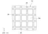
図4に示すように、実施形態の半導体装置1は、基板10と、基板10の表面10aの一部上に設けられた第1導電部材20とを備える。基板10の表面10aに平行で且つ互いに交差する(この例では直交する)2方向を第1方向X及び第2方向Y方向とする。第1方向X及び第2方向Y方向に直交し、基板10の表面10aに垂直な方向を第3方向Zとする。例えば、第1導電部材20は、第1方向X及び第2方向Y方向に沿って延び、格子状の平面パターンを有する。第1導電部材20は、基板10の表面10aに直接接している。
基板10は、例えば、シリコン基板である。基板10として、サファイア基板を用いてもよい。第1導電部材20は、例えば、ニッケル、窒化チタン、及びタングステンよりなる群から選択された少なくとも1つを含むことができる。基板10としてシリコン基板を用いた場合には、第1導電部材20はニッケルシリサイドを含むことができる。
実施形態の半導体装置1は、複数の窒化物半導体素子を備える。図1に示す例では、複数の窒化物半導体素子として、第1窒化物半導体素子101と第2窒化物半導体素子102とを示す。第1窒化物半導体素子101及び第2窒化物半導体素子102は、例えば、横型HEMT素子である。
第1窒化物半導体素子101及び第2窒化物半導体素子102は、基板10上及び第1導電部材20上に設けられ、互いに分離した複数の窒化物半導体層30を有する。第1窒化物半導体素子101は第1窒化物半導体層30Aを有し、第2窒化物半導体素子102は第2窒化物半導体層30Bを有する。本明細書において、第1窒化物半導体層30Aと第2窒化物半導体層30Bとを区別せずに、単に窒化物半導体層30とも言う。なお、基板10上において互いに素子分離された3以上の窒化物半導体層30が設けられてもよい。
第1窒化物半導体層30Aと第2窒化物半導体層30Bとは、基板10上において素子分離部300によって互いに分離されている。素子分離部300は、第1窒化物半導体層30Aの周囲及び第2窒化物半導体層30Bの周囲を連続して囲んでいる。素子分離部300は、絶縁部材であり、例えば、シリコン酸化膜を含むことができる。
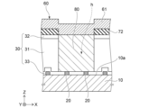
図3に示すように、窒化物半導体層30は、第1層31と第2層32とを有する。第2層32は、第3方向Zにおいて第1層31上に設けられている。第2層32のバンドギャップは、第1層31のバンドギャップよりも広い。例えば、第1層31は窒化ガリウム(GaN)層であり、第2層32は窒化アルミニウムガリウム(AlGaN)層である。第1層31における第2層32との界面近傍に2次元電子ガス35が分布する。
窒化物半導体層30は、第3層33をさらに有してもよい。第3層33は、基板10と第1層31との間、及び第1導電部材20と第1層31との間に設けられる。第3層33は、窒化物半導体層30の結晶欠陥を低減するバッファ層として機能する。第3層33として、例えば、窒化アルミニウム(AlN)層を用いることができる。
第1窒化物半導体素子101及び第2窒化物半導体素子102のそれぞれは、アクティブ領域ARを有する。図2は、アクティブ領域ARの模式平面図である。図3は、図2におけるA-A線断面図である。
第1窒化物半導体素子101及び第2窒化物半導体素子102のそれぞれは、ソース電極60、ドレイン電極40、ゲート電極50、及び第1絶縁膜71を有する。これらは、窒化物半導体層30上に設けられている。
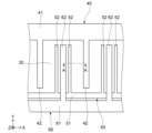
図2に示すように、ソース電極60は、ソースフィンガー部62とソースパッド部61とを有する。ソースパッド部61は第1方向Xに延びている。複数のソースフィンガー部62が、ソースパッド部61から第2方向Yに延びている。図3に示すように、ソースフィンガー部62は、窒化物半導体層30の表面に接し、窒化物半導体層30と電気的に接続されている。ソース電極60の材料として、例えば、チタン(Ti)とアルミニウム(Al)の積層構造を用いることができる。
図2に示すように、ドレイン電極40は、ドレインフィンガー部42とドレインパッド部41とを有する。ドレインパッド部41は第1方向Xに延びている。複数のドレインフィンガー部42が、ドレインパッド部41から、ソースパッド部61に向けて第2方向Yに延びている。図3に示すように、ドレインフィンガー部42は、窒化物半導体層30の表面に接し、窒化物半導体層30と電気的に接続されている。ドレイン電極40の材料として、例えば、ソース電極60と同じ材料を用いることができる。
図3に示すように、ソースフィンガー部62とドレインフィンガー部42との間の窒化物半導体層30の表面上に、第1絶縁膜71が設けられている。第1絶縁膜71として、例えば、シリコン酸化膜を用いることができる。
図2に示すように、ゲート電極50は、ゲートフィンガー部52とゲート配線部51とを有する。ゲート配線部51は第1方向Xに延びている。複数のゲートフィンガー部52が、ゲート配線部51から第2方向Yに延びている。例えば、ゲートフィンガー部52は、ゲート配線部51からドレインパッド部41に向けて延びている。ゲートフィンガー部52は、第1方向Xにおいて、ドレインフィンガー部42とソースフィンガー部62との間に位置する。第1方向Xにおいて隣り合う2つのドレインフィンガー部42の間に2つのゲートフィンガー部52が位置する。第1方向Xにおいて隣り合う2つのゲートフィンガー部52の間に、1つのソースフィンガー部62が位置する。ゲート電極50の材料として、例えば、ニッケル(Ni)と金(Au)の積層構造、窒化チタン(TiN)、又は多結晶シリコン(Poly-Si)を用いることができる。
図3に示すように、ゲートフィンガー部52は、第1絶縁膜71上に設けられている。ドレイン電極40のドレインフィンガー部42と、ゲート電極50のゲートフィンガー部52との間の第1方向Xの距離は、ソース電極60のソースフィンガー部62と、ゲート電極50のゲートフィンガー部52との間の第1方向Xの距離よりも長い。これにより、耐圧を向上できる。
第1窒化物半導体素子101及び第2窒化物半導体素子102のそれぞれは、図5に示す第2導電部材80を有する。第2導電部材80は、窒化物半導体層30内において柱状に設けられている。第2導電部材80は、第1導電部材20とソース電極60との間を延び、第1導電部材20及びソース電極60と電気的に接続されている。第2導電部材80の材料として、例えば、ニッケル(Ni)、チタン(Ti)、アルミニウム(Al)などを用いることができる。
第2導電部材80は、窒化物半導体層30に形成されたホールh内に設けられる。ホールhの底部において第1導電部材20が露出する。その露出した第1導電部材20に、第2導電部材80が接している。第2導電部材80は、例えば格子状に延びる複数本の第1導電部材20の少なくとも1本の第1導電部材20に接する。複数本の第1導電部材20は例えば格子状に連続しているため、複数本の第1導電部材20が第2導電部材80を介してソース電極60と電気的に接続される。第2導電部材80の上面は、ソース電極60のソースパッド部61に接している。
第1窒化物半導体素子101及び第2窒化物半導体素子102のそれぞれは、窒化物半導体層30の表面とソースパッド部61との間に設けられた第2絶縁膜72を有することができる。第2絶縁膜72は、窒化物半導体層30の表面とドレインパッド部41との間、及び窒化物半導体層30の表面とゲート配線部51との間にも設けられる。また、第2絶縁膜72は、後述するゲートパッド部53(図1に示す)と、窒化物半導体層30の表面との間にも設けられる。第2絶縁膜72として、例えば、シリコン酸化膜を用いることができる。
実施形態の半導体装置は、図1に示すように、第1窒化物半導体素子101及び第2窒化物半導体素子102を支持する支持部材200を備えることができる。支持部材200は、絶縁部201と導電部とを有する。絶縁部201の材料として、例えば、樹脂を用いることができる。導電部は、例えば、リードフレームであり、第1リード211、第2リード212、第3リード213、第4リード214、及び第5リード215を含む。第1リード211、第2リード212、第3リード213、第4リード214、及び第5リード215の材料として、例えば、鉄(Fe)、ニッケル(Ni)、銅(Cu)を用いることができる。
第1窒化物半導体素子101及び第2窒化物半導体素子102は、例えば、ハーフブリッジ回路を構成する。第1窒化物半導体素子101がハイサイド素子として機能し、第2窒化物半導体素子102がローサイド素子として機能する。なお、半導体装置1は、基板10上に3以上の窒化物半導体素子を有してもよい。
図1に示すように、第1窒化物半導体素子101の第1窒化物半導体層30A上に設けられたドレインパッド部41は、ワイヤwを介して、第1リード211と電気的に接続されている。第1リード211は、電源と電気的に接続される。ワイヤwとして、例えば、金ワイヤを用いることができる。
第2窒化物半導体素子102の第2窒化物半導体層30B上に設けられたソースパッド部61は、ワイヤwを介して、第2リード212と電気的に接続されている。第2リード212は接地される。
第1窒化物半導体素子101の第1窒化物半導体層30A上には、第1窒化物半導体素子101のゲート配線部51と電気的に接続されたゲートパッド部53が設けられ、第1窒化物半導体素子101のゲートパッド部53はワイヤwを介して第3リード213と電気的に接続されている。
第2窒化物半導体素子102の第2窒化物半導体層30B上には、第2窒化物半導体素子102のゲート配線部51と電気的に接続されたゲートパッド部53が設けられ、第2窒化物半導体素子102のゲートパッド部53はワイヤwを介して第4リード214と電気的に接続されている。
第1窒化物半導体素子101の第1窒化物半導体層30A上に設けられたソースパッド部61は、ワイヤwを介して第5リード215と電気的に接続されている。第2窒化物半導体素子102の第2窒化物半導体層30B上に設けられたドレインパッド部41は、ワイヤwを介して第5リード215と電気的に接続されている。したがって、第1窒化物半導体素子101のソース電極60は、第5リード215において、第2窒化物半導体素子102のドレイン電極40と電気的に接続されている。第5リード215は、ハーフブリッジ回路の出力端子となる。
または、図8に示すように、第1窒化物半導体素子101のソースパッド部61と、第2窒化物半導体素子102のドレインパッド部41とを、窒化物半導体層30の上方において素子分離部300を跨ぐように接続することで、第1窒化物半導体素子101のソース電極60と、第2窒化物半導体素子102のドレイン電極40とを電気的に接続してもよい。
図1に示す半導体装置1の上面は、例えば樹脂材料からなる封止部材で覆われる。
本実施形態によれば、複数の窒化物半導体素子101、102を同じ基板10上で実現しつつ、基板10には第2導電部材80及び第1導電部材20を介してソース電極60の電位を与えることができる。基板10の電位をソース電位に固定することで、複数の窒化物半導体素子101、102のそれぞれを、他の窒化物半導体素子の影響を受けずに動作させることができる。例えば、ローサイド素子(第2窒化物半導体素子102)のオフ時にハイサイド素子(第1窒化物半導体素子101)の裏面に負電圧がかかることによるオン抵抗の上昇を抑制できる。ソース電位は、例えば、グランド電位である。
図4に示すように、第1導電部材20は基板10の表面10aにおいて例えば格子状に延びており、その格子状の第1導電部材20の一部分が第2導電部材80に接することで、基板10の表面10aにおける第2導電部材80の配置位置以外の広い範囲にソース電位を与えることができる。第1導電部材20の平面パターンは、例えば、第1方向Xまたは第2方向Yに延びる複数本のストライプ状パターンであってもよい。その場合、ストライプ状の第1導電部材20を横切る方向に延びる少なくとも1本の第1導電部材20で、ストライプ状の第1導電部材20同士を接続することができる。
図3に示すように、第1導電部材20は、ドレイン電極40のドレインフィンガー部42の下及びゲート電極50のゲートフィンガー部52の下にも位置する。これにより、窒化物半導体層30に対して裏面側からフィールドプレート効果を与えることができ、電界の集中を緩和することが可能になる。
次に、実施形態の半導体装置の製造方法について説明する。
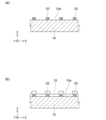
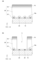
実施形態の半導体装置の製造方法は、図6(a)に示すように、基板10の表面10aの一部上に、第1導電部材20を形成する工程を備える。例えば、図4を参照して前述したように、格子状のパターンで第1導電部材20を形成することができる。
第1導電部材20を形成した後、実施形態の半導体装置の製造方法は、基板10上及び第1導電部材20上に窒化物半導体層30を形成する工程を備える。
例えば、シリコン基板である基板10上に、MOCVD(metal organic chemical vapor deposition)法により、窒化物半導体層30を形成することができる。窒化物半導体層30を基板10上に良好に成長させるために、基板10の表面10aにおいて、第1導電部材20が設けられた一部の面積は、第1導電部材20が設けられていない他の部分の面積よりも小さいことが好ましい。
例えば、図4に示す例において、第1導電部材20の第1方向Xの幅及び第2方向Yの幅は0.1μmであり、第1方向Xにおいて隣り合う第1導電部材20間の距離(ピッチ)及び第2方向Yにおいて隣り合う第1導電部材20間の距離(ピッチ)は10μmである。
窒化物半導体層30を形成する工程において、図6(b)に示すように、例えば、バッファ層として第3層33が基板10の表面10a上に形成される。基板10の表面10aから成長した第3層33は、第1導電部材20上において横方向に成長して第1導電部材20を覆うことができる。第3層33として、例えば、窒化アルミニウム層を用いることができる。
第3層33上には、図7(a)に示すように、第1層31及び第2層32が順に成長される。また、第2層32上に絶縁膜70が形成される。絶縁膜70は、前述した第1絶縁膜71及び第2絶縁膜72を含むことができる。
実施形態の半導体装置の製造方法は、窒化物半導体層30を、複数に分離する工程を備える。例えば、RIE(Reactive Ion Etching)法により、窒化物半導体層30に、図1に示す素子分離部300に沿うトレンチを形成する。トレンチは、基板10の表面10aに達する。トレンチの底部において、第1導電部材20間に第3層33が残っていてもよい。トレンチによって、窒化物半導体層30は複数に分離される。図1に示す例では、窒化物半導体層30は、第1窒化物半導体層30Aと第2窒化物半導体層30Bとに分離される。トレンチ内には、絶縁部材が埋め込まれる。窒化物半導体層30は、3以上に分離してもよい。
実施形態の半導体装置の製造方法は、図7(b)に示すように、窒化物半導体層30に、第1導電部材20に達するホールhを形成する工程を備える。ホールhは、例えば、RIE法により形成することができる。上記トレンチとホールは同時に形成することができる。ホールhは、少なくとも、絶縁膜70、第2層32、及び第1層31を第3方向Zにおいて貫通する。ホールhの底部において第1導電部材20の少なくとも上面が露出する。ホールhの底部において第1導電部材20の側面の少なくとも一部が露出してもよい。
ホールhの平面形状は例えば四角形である。ホールhの平面形状は円形であってもよい。ホールhの幅または直径は、例えば、100μmにすることができる。この場合、例えば10μm間隔(ピッチ)で第1方向Xに並ぶ複数本の第1導電部材20のうちの10本程度がホールhの底部に露出することができる。同様に、例えば10μm間隔(ピッチ)で第2方向Yに並ぶ複数本の第1導電部材20のうちの10本程度がホールhの底部に露出することができる。基板10の表面10aに例えば格子状パターンで第1導電部材20を形成し、第1導電部材20のピッチよりも大きい平面サイズのホールhを形成することで、特にマークなどを必要とせずに、窒化物半導体層30のどこにホールhを形成しても、ホールhの底部に第1導電部材20を露出させやすくできる。
実施形態の半導体装置の製造方法は、ホールh内に、第2導電部材80を形成する工程を備える。図5に示すように、第2導電部材80はホールhの底部において第1導電部材20に接する。
実施形態の半導体装置の製造方法は、窒化物半導体層30上に、第2導電部材80と電気的に接続するソース電極60を形成する工程を備える。図5に示す例では、ソース電極60のソースパッド部61が第2導電部材80の上面に接する。これにより、第1導電部材20は、第2導電部材80を介してソース電極60と電気的に接続される。
第1導電部材20を形成する工程において、基板10がシリコン基板の場合、第1導電部材20はニッケルを含むことが好ましい。第1導電部材20を形成した後、基板10のシリコンと第1導電部材20のニッケルとを熱反応させ、第1導電部材20をニッケルシリサイド化することができる。ニッケルシリサイドの格子定数は、シリコンの格子定数と近いため、窒化物半導体層30を形成する工程において、第1導電部材20の上にも窒化物半導体層30を欠陥を低減して形成しやすくできる。
例えば、MOCVD法により窒化物半導体層30を形成する工程において加わる熱により、第1導電部材20をニッケルシリサイド化しつつ、ニッケルシリサイド上に窒化物半導体層30を成長させることができる。
第1導電部材20の第3方向Zの厚さ(高さ)を小さくすることで、窒化物半導体層30の平坦性を確保しやすい。また、第1導電部材20の厚さには、ホールhを形成するエッチングの際に第1導電部材20が消失せずに確実に残る厚さが求められる。このような観点から、第1導電部材20の第3方向Zにおける厚さ(高さ)は、10nm以上100nm以下が好ましい。
本発明のいくつかの実施形態を説明したが、これらの実施形態は、例として提示したものであり、発明の範囲を限定することは意図していない。これら新規な実施形態は、その他の様々な形態で実施されることが可能であり、発明の要旨を逸脱しない範囲で、種々の省略、置き換え、変更を行うことができる。これら実施形態やその変形は、発明の範囲や要旨に含まれるとともに、特許請求の範囲に記載された発明とその均等の範囲に含まれる。
1…半導体装置、10…基板、20…第1導電部材、30…窒化物半導体層、30A…第1窒化物半導体層、30B…第2窒化物半導体層、31…第1層、32…第2層、33…第3層、35…2次元電子ガス、40…ドレイン電極、41…ドレインパッド部、42…ドレインフィンガー部、50…ゲート電極、51…ゲート配線部、52…ゲートフィンガー部、53…ゲートパッド部、60…ソース電極、61…ソースパッド部、62…ソースフィンガー部、101…第1窒化物半導体素子、102…第2窒化物半導体素子、200…支持部材、211…第1リード、212…第2リード、213…第3リード、214…第4リード、215…第5リード、300…素子分離部、h…ホール、AR…アクティブ領域
Claims (11)
- 基板と、
前記基板の表面の一部上に設けられた第1導電部材と、
前記基板上及び前記第1導電部材上に設けられ、互いに分離した複数の窒化物半導体層と、
前記窒化物半導体層上に設けられたソース電極と、
前記窒化物半導体層上に設けられたドレイン電極と、
前記窒化物半導体層上に設けられたゲート電極と、
前記窒化物半導体層内において前記第1導電部材と前記ソース電極との間を延び、前記第1導電部材及び前記ソース電極と電気的に接続された第2導電部材と、
を備える半導体装置。 - 前記基板の前記表面において、前記第1導電部材が設けられた前記一部の面積は、前記第1導電部材が設けられていない他の部分の面積よりも小さい請求項1に記載の半導体装置。
- 前記第1導電部材は、前記基板の前記表面に平行で且つ互いに交差する2方向に沿って延びている請求項1または2に記載の半導体装置。
- 前記窒化物半導体層は、第1層と、前記第1層上に設けられ、前記第1層よりもバンドギャップが広い第2層とを有する請求項1または2に記載の半導体装置。
- 前記複数の窒化物半導体層は、第1窒化物半導体層と第2窒化物半導体層とを有し、
前記第1窒化物半導体層上に設けられた前記ソース電極は、前記第2窒化物半導体層上に設けられた前記ドレイン電極と電気的に接続されている請求項1または2に記載の半導体装置。 - 前記第1導電部材は、前記ドレイン電極の下及び前記ゲート電極の下にも位置する請求項1または2に記載の半導体装置。
- 前記基板は、シリコン基板であり、
前記第1導電部材は、ニッケルシリサイドを含む請求項1または2に記載の半導体装置。 - 前記ドレイン電極と前記ゲート電極との間の距離は、前記ソース電極と前記ゲート電極との間の距離よりも長い請求項1または2に記載の半導体装置。
- 基板の表面の一部上に、第1導電部材を形成する工程と、
前記基板上及び前記第1導電部材上に、窒化物半導体層を形成する工程と、
前記窒化物半導体層を、複数に分離する工程と、
前記窒化物半導体層に、前記第1導電部材に達するホールを形成する工程と、
前記ホール内に、前記第1導電部材に接する第2導電部材を形成する工程と、
前記窒化物半導体層上に、前記第2導電部材と電気的に接続するソース電極を形成する工程と、
を備える半導体装置の製造方法。 - 前記基板は、シリコン基板であり、
前記第1導電部材は、ニッケルを含み、
シリコンとニッケルを熱反応させ、前記第1導電部材をニッケルシリサイド化する請求項9に記載の半導体装置の製造方法。 - 前記窒化物半導体層を形成する工程において加わる熱により、前記第1導電部材をニッケルシリサイド化する請求項10に記載の半導体装置の製造方法。
Priority Applications (4)
| Application Number | Priority Date | Filing Date | Title |
|---|---|---|---|
| CN202380099489.XA CN121336508A (zh) | 2023-09-20 | 2023-09-20 | 半导体装置及其制造方法 |
| JP2025547044A JPWO2025062529A1 (ja) | 2023-09-20 | 2023-09-20 | |
| PCT/JP2023/034096 WO2025062529A1 (ja) | 2023-09-20 | 2023-09-20 | 半導体装置及びその製造方法 |
| US19/409,636 US20260090077A1 (en) | 2023-09-20 | 2025-12-04 | Semiconductor device and method for manufacturing same |
Applications Claiming Priority (1)
| Application Number | Priority Date | Filing Date | Title |
|---|---|---|---|
| PCT/JP2023/034096 WO2025062529A1 (ja) | 2023-09-20 | 2023-09-20 | 半導体装置及びその製造方法 |
Related Child Applications (1)
| Application Number | Title | Priority Date | Filing Date |
|---|---|---|---|
| US19/409,636 Continuation US20260090077A1 (en) | 2023-09-20 | 2025-12-04 | Semiconductor device and method for manufacturing same |
Publications (1)
| Publication Number | Publication Date |
|---|---|
| WO2025062529A1 true WO2025062529A1 (ja) | 2025-03-27 |
Family
ID=95072385
Family Applications (1)
| Application Number | Title | Priority Date | Filing Date |
|---|---|---|---|
| PCT/JP2023/034096 Pending WO2025062529A1 (ja) | 2023-09-20 | 2023-09-20 | 半導体装置及びその製造方法 |
Country Status (4)
| Country | Link |
|---|---|
| US (1) | US20260090077A1 (ja) |
| JP (1) | JPWO2025062529A1 (ja) |
| CN (1) | CN121336508A (ja) |
| WO (1) | WO2025062529A1 (ja) |
Citations (5)
| Publication number | Priority date | Publication date | Assignee | Title |
|---|---|---|---|---|
| JP2008235738A (ja) * | 2007-03-23 | 2008-10-02 | Furukawa Electric Co Ltd:The | GaN系半導体素子 |
| JP2015032675A (ja) * | 2013-08-01 | 2015-02-16 | 株式会社東芝 | 半導体装置 |
| JP2015149324A (ja) * | 2014-02-05 | 2015-08-20 | ルネサスエレクトロニクス株式会社 | 半導体装置 |
| JP2020198327A (ja) * | 2019-05-30 | 2020-12-10 | ローム株式会社 | 窒化物半導体装置 |
| WO2023048160A1 (ja) * | 2021-09-22 | 2023-03-30 | エア・ウォーター株式会社 | 半導体基板、半導体デバイス、半導体基板の製造方法、および半導体デバイスの製造方法 |
-
2023
- 2023-09-20 JP JP2025547044A patent/JPWO2025062529A1/ja active Pending
- 2023-09-20 WO PCT/JP2023/034096 patent/WO2025062529A1/ja active Pending
- 2023-09-20 CN CN202380099489.XA patent/CN121336508A/zh active Pending
-
2025
- 2025-12-04 US US19/409,636 patent/US20260090077A1/en active Pending
Patent Citations (5)
| Publication number | Priority date | Publication date | Assignee | Title |
|---|---|---|---|---|
| JP2008235738A (ja) * | 2007-03-23 | 2008-10-02 | Furukawa Electric Co Ltd:The | GaN系半導体素子 |
| JP2015032675A (ja) * | 2013-08-01 | 2015-02-16 | 株式会社東芝 | 半導体装置 |
| JP2015149324A (ja) * | 2014-02-05 | 2015-08-20 | ルネサスエレクトロニクス株式会社 | 半導体装置 |
| JP2020198327A (ja) * | 2019-05-30 | 2020-12-10 | ローム株式会社 | 窒化物半導体装置 |
| WO2023048160A1 (ja) * | 2021-09-22 | 2023-03-30 | エア・ウォーター株式会社 | 半導体基板、半導体デバイス、半導体基板の製造方法、および半導体デバイスの製造方法 |
Also Published As
| Publication number | Publication date |
|---|---|
| JPWO2025062529A1 (ja) | 2025-03-27 |
| US20260090077A1 (en) | 2026-03-26 |
| CN121336508A (zh) | 2026-01-13 |
Similar Documents
| Publication | Publication Date | Title |
|---|---|---|
| TWI525753B (zh) | 利用島狀形貌之氮化鎵功率器件 | |
| US8916962B2 (en) | III-nitride transistor with source-connected heat spreading plate | |
| JP7470848B2 (ja) | 半導体装置 | |
| US20210265477A1 (en) | III-Nitride Transistor With A Cap Layer For RF Operation | |
| WO2020032206A1 (ja) | SiC半導体装置 | |
| JP2013187546A (ja) | 高電子移動度トランジスタ及びその製造方法 | |
| JPWO2020255259A1 (ja) | 半導体装置およびその製造方法 | |
| CN107768438B (zh) | 半导体装置 | |
| JP7095982B2 (ja) | 半導体装置 | |
| JP7655485B2 (ja) | 電界効果トランジスタ、その製造方法、及び電子回路 | |
| CN116504759B (zh) | 一种半导体器件及其制备方法 | |
| KR20210132573A (ko) | 반도체 디바이스를 위한 기판 손실 감소 | |
| CN113224153A (zh) | 高电子迁移率晶体管及其制作方法 | |
| CN114503261B (zh) | 氮化物基半导体电路及其制造方法 | |
| CN117981087A (zh) | 降低漏电流的氮化镓半导体装置及其制造方法 | |
| US20240395920A1 (en) | High electron mobility transistor and its manufacturing method | |
| WO2025062529A1 (ja) | 半導体装置及びその製造方法 | |
| KR100797169B1 (ko) | 반도체 디바이스 및 그 형성 방법 | |
| CN216213472U (zh) | 半导体装置 | |
| KR101402147B1 (ko) | 갈륨 질화물계 반도체 소자, 이의 제조 방법 및 이를 포함하는 파워 모듈 | |
| KR20150039481A (ko) | 전력 반도체 소자 | |
| US20250351414A1 (en) | Semiconductor device | |
| TWI849920B (zh) | 高電子遷移率電晶體及其製造方法 | |
| KR101392398B1 (ko) | 갈륨 질화물계 반도체 소자, 이의 제조 방법 및 이를 포함하는 파워 모듈 | |
| US20240194746A1 (en) | Vertical Semiconductor Power Device and Method for Manufacturing the Same |
Legal Events
| Date | Code | Title | Description |
|---|---|---|---|
| ENP | Entry into the national phase |
Ref document number: 2025547044 Country of ref document: JP Kind code of ref document: A |