WO2025057740A1 - エッチング方法およびエッチング装置 - Google Patents
エッチング方法およびエッチング装置 Download PDFInfo
- Publication number
- WO2025057740A1 WO2025057740A1 PCT/JP2024/030794 JP2024030794W WO2025057740A1 WO 2025057740 A1 WO2025057740 A1 WO 2025057740A1 JP 2024030794 W JP2024030794 W JP 2024030794W WO 2025057740 A1 WO2025057740 A1 WO 2025057740A1
- Authority
- WO
- WIPO (PCT)
- Prior art keywords
- etching
- gas
- substrate
- temperature
- sige
- Prior art date
- Legal status (The legal status is an assumption and is not a legal conclusion. Google has not performed a legal analysis and makes no representation as to the accuracy of the status listed.)
- Ceased
Links
Images






Classifications
-
- H—ELECTRICITY
- H10—SEMICONDUCTOR DEVICES; ELECTRIC SOLID-STATE DEVICES NOT OTHERWISE PROVIDED FOR
- H10P—GENERIC PROCESSES OR APPARATUS FOR THE MANUFACTURE OR TREATMENT OF DEVICES COVERED BY CLASS H10
- H10P50/00—Etching of wafers, substrates or parts of devices
- H10P50/20—Dry etching; Plasma etching; Reactive-ion etching
- H10P50/24—Dry etching; Plasma etching; Reactive-ion etching of semiconductor materials
- H10P50/242—Dry etching; Plasma etching; Reactive-ion etching of semiconductor materials of Group IV materials
-
- H—ELECTRICITY
- H01—ELECTRIC ELEMENTS
- H01J—ELECTRIC DISCHARGE TUBES OR DISCHARGE LAMPS
- H01J37/00—Discharge tubes with provision for introducing objects or material to be exposed to the discharge, e.g. for the purpose of examination or processing thereof
- H01J37/32—Gas-filled discharge tubes
- H01J37/32431—Constructional details of the reactor
- H01J37/3244—Gas supply means
- H01J37/32449—Gas control, e.g. control of the gas flow
-
- H—ELECTRICITY
- H01—ELECTRIC ELEMENTS
- H01J—ELECTRIC DISCHARGE TUBES OR DISCHARGE LAMPS
- H01J37/00—Discharge tubes with provision for introducing objects or material to be exposed to the discharge, e.g. for the purpose of examination or processing thereof
- H01J37/32—Gas-filled discharge tubes
- H01J37/32431—Constructional details of the reactor
- H01J37/32715—Workpiece holder
- H01J37/32724—Temperature
-
- H—ELECTRICITY
- H10—SEMICONDUCTOR DEVICES; ELECTRIC SOLID-STATE DEVICES NOT OTHERWISE PROVIDED FOR
- H10P—GENERIC PROCESSES OR APPARATUS FOR THE MANUFACTURE OR TREATMENT OF DEVICES COVERED BY CLASS H10
- H10P50/00—Etching of wafers, substrates or parts of devices
-
- H—ELECTRICITY
- H10—SEMICONDUCTOR DEVICES; ELECTRIC SOLID-STATE DEVICES NOT OTHERWISE PROVIDED FOR
- H10P—GENERIC PROCESSES OR APPARATUS FOR THE MANUFACTURE OR TREATMENT OF DEVICES COVERED BY CLASS H10
- H10P50/00—Etching of wafers, substrates or parts of devices
- H10P50/20—Dry etching; Plasma etching; Reactive-ion etching
- H10P50/26—Dry etching; Plasma etching; Reactive-ion etching of conductive or resistive materials
- H10P50/264—Dry etching; Plasma etching; Reactive-ion etching of conductive or resistive materials by chemical means
- H10P50/266—Dry etching; Plasma etching; Reactive-ion etching of conductive or resistive materials by chemical means by vapour etching only
-
- H—ELECTRICITY
- H10—SEMICONDUCTOR DEVICES; ELECTRIC SOLID-STATE DEVICES NOT OTHERWISE PROVIDED FOR
- H10P—GENERIC PROCESSES OR APPARATUS FOR THE MANUFACTURE OR TREATMENT OF DEVICES COVERED BY CLASS H10
- H10P72/00—Handling or holding of wafers, substrates or devices during manufacture or treatment thereof
- H10P72/04—Apparatus for manufacture or treatment
- H10P72/0402—Apparatus for fluid treatment
- H10P72/0418—Apparatus for fluid treatment for etching
- H10P72/0421—Apparatus for fluid treatment for etching for drying etching
-
- H—ELECTRICITY
- H10—SEMICONDUCTOR DEVICES; ELECTRIC SOLID-STATE DEVICES NOT OTHERWISE PROVIDED FOR
- H10P—GENERIC PROCESSES OR APPARATUS FOR THE MANUFACTURE OR TREATMENT OF DEVICES COVERED BY CLASS H10
- H10P72/00—Handling or holding of wafers, substrates or devices during manufacture or treatment thereof
- H10P72/04—Apparatus for manufacture or treatment
- H10P72/0431—Apparatus for thermal treatment
- H10P72/0434—Apparatus for thermal treatment mainly by convection
-
- H—ELECTRICITY
- H10—SEMICONDUCTOR DEVICES; ELECTRIC SOLID-STATE DEVICES NOT OTHERWISE PROVIDED FOR
- H10P—GENERIC PROCESSES OR APPARATUS FOR THE MANUFACTURE OR TREATMENT OF DEVICES COVERED BY CLASS H10
- H10P72/00—Handling or holding of wafers, substrates or devices during manufacture or treatment thereof
- H10P72/06—Apparatus for monitoring, sorting, marking, testing or measuring
- H10P72/0602—Temperature monitoring
-
- H—ELECTRICITY
- H01—ELECTRIC ELEMENTS
- H01J—ELECTRIC DISCHARGE TUBES OR DISCHARGE LAMPS
- H01J2237/00—Discharge tubes exposing object to beam, e.g. for analysis treatment, etching, imaging
- H01J2237/32—Processing objects by plasma generation
- H01J2237/33—Processing objects by plasma generation characterised by the type of processing
- H01J2237/334—Etching
Definitions
- This disclosure relates to an etching method and an etching apparatus.
- Patent Document 1 proposes a technique for selectively etching such SiGe and Ge relative to Si using a processing gas containing a fluorine-containing gas and a hydrogen-containing gas.
- the present disclosure provides an etching method and an etching apparatus that can etch SiGe or Ge with high controllability.
- An etching method includes providing a substrate having SiGe or Ge on its surface in a chamber, supplying an etching gas for etching the SiGe or Ge to the substrate held at a first temperature at which no etching reaction occurs, so that the etching gas is adsorbed onto the surface of the substrate, and raising the temperature of the substrate to a second temperature at which a reaction occurs between the SiGe or Ge and the etching gas, thereby etching the SiGe or Ge.
- the present disclosure provides an etching method and an etching apparatus that can etch SiGe or Ge with high controllability.
- FIG. 1 is a flowchart illustrating a specific example of an etching method according to an embodiment.
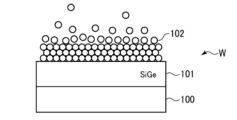
- 4 is a cross-sectional view showing an example of a state of a substrate when step ST2 of the etching method of the embodiment is performed;
- FIG. 1 is a cross-sectional view showing a schematic example of a state of a substrate when step ST3 of an etching method according to an embodiment is performed;
- 1 is a cross-sectional view showing an example of a state of a substrate when step ST4 of an etching method according to an embodiment is performed;
- 4 is a timing chart showing a typical example of a process sequence of steps ST2 to ST5 in an etching method according to an embodiment.
- FIG. 11 is a graph showing the results of an evaluation test.
- 1 is a SEM image showing the results of an evaluation test.
- 1 is a SEM image showing the results of an evaluation test.
- 1 is a SEM image showing the results of an evaluation test.
- 1 is a SEM image showing the results of an evaluation test.
- 1 is a SEM image showing the results of an evaluation test.
- FIG. 1 is a flow chart showing a specific example of an etching method according to one embodiment.
- a substrate having SiGe or Ge on its surface is placed in a chamber for performing an etching process (step ST1).
- step ST5 the residues resulting from the etching are removed from the chamber.
- the desired amount of etching is performed on the SiGe or Ge.
- the ratio of Si and Ge in SiGe is arbitrary, but it is preferable that Si is 90 at % or less.
- the form of SiGe and Ge is not particularly limited, but an example is one formed as a film, and an example of the film is one formed by a chemical vapor deposition (CVD) method.
- the substrate is not particularly limited, but an example is a semiconductor wafer (hereinafter simply referred to as a wafer).
- the substrate is not particularly limited, but examples include substrates that contain Si in the portion that comes into contact with the etching gas during processing in addition to SiGe or Ge. In this case, it is desirable to selectively etch SiGe or Ge relative to Si.
- Si may be doped with B, P, C, As, etc.
- step ST2 when a processing gas including an etching gas is supplied to the substrate surface for adsorption, the etching gas is adsorbed until it is saturated on the surface of the SiGe or Ge to be etched.
- the etching gas 102 is adsorbed on the surface of the SiGe film 101 formed on the semiconductor base 100 in the substrate W until it is saturated.
- the processing gas may contain an inert gas such as N 2 gas or Ar gas as a dilution gas or carrier gas.
- the inert gas can also be used as a purge gas.
- the etching gas is not particularly limited as long as it can etch SiGe or Ge.
- a fluorine-containing gas can be used.
- the fluorine-containing gas is suitable for etching SiGe or Ge with a high selectivity to Si.
- the fluorine-containing gas can be ClF3 gas, F2 gas, SF6 gas, or IF7 gas, and at least one of these can be used.
- the etching gas can be adsorbed without causing an etching reaction by setting the first temperature lower than the boiling point of the etching product.
- the etching product is a reaction product of the etching gas with SiGe or Ge, and is a compound containing Ge and F. If the first temperature is too low, the energy used to change the temperature between the first temperature and the second temperature becomes large, and the time required for the temperature change also becomes long. From the viewpoint of adsorbing the etching gas as described above and avoiding excessive cooling of the substrate, the first temperature is preferably -40°C or higher and -20°C or lower.
- the substrate temperature can be controlled using a temperature control mechanism such as a cooling mechanism or a heating mechanism that is provided on the stage on which the substrate is placed.
- the substrate temperature can be controlled with high precision by using an electrostatic chuck to hold the substrate using electrostatic force.
- the pressure when performing step ST2 is appropriately set according to the etching gas used.
- the etching gas is a fluorine-containing gas, for example, F2 gas
- a range of 0.01 to 1 Torr (1.33 to 133 Pa) is preferable.
- the time for step ST2 may be a time that allows the etching gas to be adsorbed to the surface of the SiGe or Ge to be etched until it is saturated, for example, 10 to 300 sec.
- the etching gas is a fluorine-containing gas, for example, F2 gas
- a time longer than 30 sec is preferable, as shown in the test results described later.
- step ST3 the etching gas is exhausted from the chamber, thereby removing excess etching gas 102 adsorbed on the surface of the substrate in step ST2.
- the amount of etching gas 102 adsorbed on the surface of the SiGe film 101 is controlled to, for example, one atomic layer or one molecular layer.
- the method for exhausting the etching gas in step ST3, can be performed by purging the chamber with an inert gas.
- the etching gas may be exhausted by evacuating the chamber.
- step ST4 the temperature of the substrate is changed from the first temperature to the second temperature while the etching gas is adsorbed on the surface of the SiGe or Ge in step ST3, and the SiGe or Ge is etched. That is, by changing the temperature of the substrate to the second temperature, a reaction occurs between the SiGe or Ge and the adsorbed etching gas. At this time, since the etching gas is adsorbed before the etching reaction occurs, the SiGe or Ge can be etched with high controllability. In addition, since the adsorption amount of the etching gas is controlled in step ST3, the etching amount can be controlled with higher accuracy. In the example shown in FIG.
- the etching gas 102 adsorbed on the surface of the SiGe film 101 is controlled to one atomic layer or one molecular layer, and when the etching reaction occurs from this state, as shown in FIG. 4, the SiGe film 101 can be etched with high accuracy by an amount corresponding to the adsorption amount of the etching gas.
- 103 is the etched portion of the SiGe film 101.
- the etching reaction can be caused by setting the second temperature to a temperature equal to or higher than the boiling point of the etching product described above.
- the boiling point here includes the sublimation point.
- the second temperature is a temperature higher than the first temperature described above, and is preferably -20°C or higher.
- the temperature adjustment mechanism provided on the shower head which is a gas ejection unit provided opposite the mounting table, may be used to change the temperature of the substrate by lifting the substrate with a lift pin provided on the mounting table.
- it is also possible to change the temperature of the substrate by supplying gas to the substrate, or by using plasma generated by a plasma generation unit.
- the pressure when performing step ST4 is appropriately set according to the etching gas used.
- the etching gas is a fluorine-containing gas, for example, F2 gas
- the pressure is preferably in the range of 0.01 to 3 Torr (1.33 to 400 Pa).
- the time of step ST4 is set to a time that allows the adsorbed etching gas to react appropriately with SiGe or Ge.
- the etching gas is a fluorine-containing gas, for example, F2 gas
- the time is preferably longer than 30 sec.
- the time of step ST4 is set so that etching of Si is suppressed as much as possible.
- the method for step ST5 is not limited as long as it can evacuate the chamber from the residues produced by etching. For example, it can be performed by drawing a vacuum inside the chamber.
- the chamber may also be purged with an inert gas before drawing a vacuum.
- step ST2 the etching gas is turned ON while the substrate is maintained at a first temperature, and the etching gas is adsorbed.
- step ST3 the etching gas is turned OFF and the purge gas is turned ON to purge the chamber.
- step ST4 the temperature of the substrate is raised to a second temperature to allow the etching reaction to proceed.
- step ST5 the chamber is evacuated to remove any residue within the chamber.
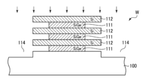
- Fig. 6 is a cross-sectional view showing an example of the structure of a wafer, which is a substrate to which the etching method of one embodiment is applied.
- the wafer W in Fig. 6 has a laminated structure 113 in which a SiGe film 111 and a Si film 112 are alternately laminated on the surface of a semiconductor substrate 100 made of, for example, Si.
- a recess 114 is formed in the laminated structure 113 by plasma etching, and the side surfaces of the alternately laminated SiGe film 111 and Si film 112 are exposed in the recess 114.
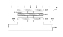
- the SiGe film 111 is side-etched and selectively etched with respect to the Si film 112 as shown in Fig. 7.
- Fig. 7 shows a state in which the SiGe film 111 is partially etched, but it may be entirely etched as shown in Fig. 8. Even if it is entirely etched, the remaining Si film 112 is supported by support columns 115 made of SiN or the like.
- the etching gas is adsorbed onto the surface of the substrate, and then the amount of adsorption is controlled, and the temperature of the substrate is raised from a first temperature to a second temperature to cause an etching reaction, thereby enabling the SiGe or Ge present on the surface of the substrate to be etched with high controllability.
- the amount of etching gas adsorbed on the SiGe or Ge surface is controlled, and then the temperature is changed to allow the etching reaction to proceed, so that the amount of etching per time is a very small amount corresponding to the amount of adsorbed etching gas, allowing etching to be performed with high controllability. Then, by performing steps ST2 to ST5 once or multiple times, etching can be performed with the desired amount of etching. Specifically, roughness control during etching is possible, and it is also possible to control the amount of etching by a small amount. It is also possible to suppress loading in coarse and dense patterns and top/bottom loading.
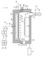
- the etching apparatus 1 includes a chamber 10 having a sealed structure.
- a mounting table 12 on which a substrate W is horizontally mounted is provided inside the chamber 10.
- the substrate W has SiGe or Ge on its surface, and has, for example, the structure shown in Fig. 6.
- the etching apparatus 1 also includes a gas supply mechanism 13 that supplies an etching gas to the chamber 10, an exhaust mechanism 14 that exhausts the inside of the chamber 10, and a control unit 15.
- the chamber 10 is composed of a chamber body 21 and a lid portion 22.
- the chamber body 21 has a roughly cylindrical side wall portion 21a and a bottom portion 21b, and the top is open, which is closed by the lid portion 22.
- the side wall portion 21a and the lid portion 22 are sealed by a sealing member (not shown), ensuring airtightness within the chamber 10.
- the lid portion 22 has a lid member 25 that forms the outer side, and a shower head 26 that is fitted inside the lid member 25 and is provided so as to face the mounting table 12.
- the shower head 26 has a main body 27 that has a cylindrical side wall 27a and an upper wall 27b, and a shower plate 28 that is provided at the bottom of the main body 27. A space 29 is formed between the main body 27 and the shower plate 28.
- a gas inlet passage 31 is formed in the lid member 25 and the upper wall 27b of the main body 27, penetrating into the space 29, and this gas inlet passage 31 is connected to a pipe 49 of the gas supply mechanism 13, which will be described later.
- the shower plate 28 has multiple gas discharge holes 32 formed therein, and gas introduced into the space 29 via the piping 49 and the gas introduction path 31 is discharged from the gas discharge holes 32 into the space within the chamber 10.
- the side wall portion 21a is provided with a loading/unloading opening 23 for loading and unloading the substrate W, and this loading/unloading opening 23 can be opened and closed by a gate valve 24.
- the mounting table 12 is generally circular in plan view and is fixed to the bottom 21b of the chamber 10.
- a temperature control mechanism 35 is provided inside the mounting table 12 to adjust the temperature of the mounting table 12 and control the temperature of the substrate W placed on it.
- the temperature control mechanism 35 has, for example, a heater and a pipe through which a low-temperature cooling medium circulates, making it possible to control the temperature of the substrate W.
- the mounting table 12 may be provided with an electrostatic chuck that attracts the substrate W by electrostatic force. By attracting the substrate W, the temperature control mechanism 35 can control the temperature of the substrate W with high precision.
- the mounting table 12 has built-in lift pins (not shown) that are used when transporting the substrate W.
- the substrate temperature can be changed from the first temperature to the second temperature by changing the controlled temperature of the temperature adjustment mechanism 35.
- a temperature adjustment mechanism may be provided in the shower head 26 provided opposite the mounting table 12, and the temperature of the substrate may be changed by lifting the substrate W with a lift pin (not shown) provided on the mounting table 12.
- the gas supply mechanism 13 supplies a process gas including an etching gas, and in this example, supplies F2 gas, which is a fluorine-containing gas, as the etching gas.
- F2 gas which is a fluorine-containing gas
- an inert gas is also supplied as the process gas.
- N2 gas is supplied as the inert gas.
- the inert gas is used as a carrier gas, a dilution gas, and a purge gas.
- the gas supply mechanism 13 has an F2 gas supply source 45 that supplies F2 gas, which is an etching gas, and an N2 gas supply source 46 that supplies N2 gas, which is an inert gas, to which one end of an F2 gas supply pipe 41 and an N2 gas supply pipe 42 are connected, respectively.
- the other end of the F2 gas supply pipe 41 and the N2 gas supply pipe 42 are connected to a common pipe 49, and the pipe 49 is connected to the above-mentioned gas introduction passage 31.
- the F2 gas supply pipe 41 and the N2 gas supply pipe 42 are provided with flow rate control units 41a and 42a, respectively, that open and close the flow passages and control the flow rate.
- the flow rate control sections 41a and 42a are constituted by, for example, an on-off valve and a flow rate control device such as a mass flow controller.
- F 2 gas as an etching gas and N 2 gas as an inert gas are supplied from gas supply sources 45 , 46 through pipes 41 , 42 , 49 into the shower head 26 and discharged from the gas discharge holes 32 of the shower plate 28 into the chamber 10 .
- the exhaust mechanism 14 has an exhaust pipe 52 connected to an exhaust port 51 formed in the bottom 21b of the chamber 10, and further has an automatic pressure control valve (APC) 53 for controlling the pressure inside the chamber 10 and a vacuum pump 54 for exhausting the inside of the chamber 10, both of which are provided on the exhaust pipe 52.
- APC automatic pressure control valve
- Two capacitance manometers 56a, 56b for high and low pressure are provided on the side wall of the chamber 10 as pressure gauges for measuring the pressure inside the chamber 10, and are inserted into the chamber 10. Based on the detection values of the capacitance manometers 56a, 56b, the opening of the automatic pressure control valve (APC) 53 is adjusted to control the pressure inside the chamber 10.
- APC automatic pressure control valve
- the control unit 15 is typically made up of a computer, and has a main control unit with a CPU that controls each component of the etching apparatus 1.
- the control unit 15 also has an input device (keyboard, mouse, etc.), an output device (printer, etc.), a display device (display, etc.), and a storage device (storage medium) connected to the main control unit.
- the main control unit of the control unit 15 controls the operation of the etching apparatus 1 based on a processing recipe stored in, for example, a storage medium built into the storage device or a storage medium set in the storage device.
- the substrate W is carried into the chamber 10 and placed on the mounting table 12.
- the temperature of the mounting table 12 is controlled by a temperature control mechanism 35, and the temperature of the substrate W is set to a first temperature at which no etching reaction occurs.
- the first temperature is set by the temperature control mechanism 35 of the mounting table 12 to a temperature lower than the boiling point of the etching product, preferably -40°C to -20°C.
- the pressure inside the chamber 10 is controlled to a pressure in the range of, for example, 0.01 to 1 Torr (1.33 to 133 Pa).
- a processing gas containing F2 gas which is a fluorine-containing gas, as an etching gas is supplied into the chamber 10.
- F2 gas which is a fluorine-containing gas
- F2 gas is adsorbed on the surface of the substrate W held at the first temperature.
- N2 gas which is an inert gas
- the adsorption process of F2 gas is performed until it is saturated on the surface of SiGe or Ge, which is the etching target present on the surface of the substrate W.
- the time for this process is preferably longer than 30 sec.
- the supply of F2 gas is stopped, and, for example, N2 gas is supplied into the chamber 10 to purge the chamber 10, thereby discharging the F2 gas adsorbed on the substrate W from the chamber 10 and controlling the amount of adsorption of F2 gas.
- the temperature of the substrate W is increased from the first temperature to a second temperature to cause a reaction between the SiGe or Ge of the substrate W and the adsorbed etching gas, and to proceed with etching of the SiGe or Ge.
- the second temperature is set to be equal to or higher than the boiling point of the etching product, and is preferably set to be equal to or higher than -20°C.
- the pressure within the chamber 10 is controlled to be within the range of, for example, 0.01 to 3 Torr (1.33 to 400 Pa).
- the substrate temperature can be changed from the first temperature to the second temperature by changing the control temperature of the temperature adjustment mechanism 35, as described above.
- the temperature of the substrate W may be changed by lifting the substrate W with lift pins, supplying gas to the substrate W, or using plasma, without changing the control temperature of the temperature adjustment mechanism 35.
- the etching time is preferably longer than 30 sec. As shown in FIG. 6, when the substrate W has a structure in which SiGe or Ge and Si coexist, the etching time is set so as to suppress etching of Si as much as possible.
- the chamber 10 is evacuated by the exhaust mechanism 14 to remove any residues resulting from etching from the chamber.
- the above process is performed once or multiple times a predetermined number of times to etch the SiGe or Ge to the desired extent. After etching is completed, the substrate W is removed from the chamber 10.
- the processing is performed by changing the temperature of the substrate W in one chamber 10. Therefore, when the temperature of the substrate W is changed by the temperature adjustment mechanism 35 and the processing is performed, if the second temperature is too high, it takes a long time to process the substrate W at the first temperature when processing one substrate W by repeating steps ST2 to ST5 or when multiple substrates W are sequentially loaded into the chamber 10 and processed. In other words, after processing the substrate W at the second temperature, it takes a long time to cool each part in the chamber 10 to process the substrate W at the first temperature.
- the second temperature mentioned above is, for example, below room temperature, and more specifically, it is preferable that it is, for example, below 5°C. Therefore, the second temperature is, for example, -20°C to 5°C.
- the above room temperature is the temperature of the clean room in which the etching apparatus 1 is placed, for example, 24°C.
- the first temperature and the second temperature have only a slight difference from the boiling point of the etching product; for example, the first temperature is set to -1°C or less than the boiling point, and the second temperature is set to +1°C or less than the boiling point (so the difference between the first temperature and the second temperature is set to 2°C or less). In this way, by setting the first temperature and the second temperature respectively near the boiling point of the etching product, it is possible to quickly adjust the temperature between the first and second temperatures.
- the first temperature and the second temperature can be set based on the boiling point of the etching product.
- this boiling point if the substance of the etching product produced by the reaction is known, the boiling point of that substance can be set at the pressure inside the chamber 10 when the substrate W is heated to the second temperature. Even if the substance of the etching product is unknown, the boiling point can be determined by performing a preliminary test before processing the substrate W in the etching device 1. In the preliminary test, the pressure inside the chamber 10 is set to the pressure when the substrate W is heated to the second temperature during actual processing, and the substrate W that has been sufficiently cooled and supplied with etching gas is heated to cause the etching reaction. The temperature at which this etching reaction is recognized to have occurred can be set to the boiling point.
- the etching apparatus 1A includes a first module that performs steps ST2 and ST3, and a second module that performs steps ST4 and ST5.
- the first module has the same configuration as the etching apparatus 1
- the second module has the same configuration as the etching apparatus 1 except that an etching gas is not supplied.
- the etching apparatus 1A includes a chamber 10 for processing the substrate W at a first temperature and a chamber 10 for processing the substrate W at a second temperature, separately.
- the etching apparatus 1A includes a transport path for the substrate W that connects the chamber 10 of the first module and the chamber 10 of the second module to form a vacuum atmosphere, and a transport mechanism that can move along the transport path.
- the substrate W is repeatedly moved back and forth between the chambers 10 by the transport mechanism, and a cycle consisting of steps ST2 to ST5 is repeated.
- the apparatus may be configured such that it is not necessary to change the temperature of the substrate W between the first and second temperatures in one chamber 10. Note that, because of the apparatus configuration described above, the etching apparatus 1A can maintain a vacuum atmosphere around the substrate W while the above cycle is repeated, just like the etching apparatus 1.
- the substrate W is processed by creating a vacuum atmosphere around it.
- the vacuuming in step ST5 is performed by evacuating the chamber 10 so that a higher vacuum atmosphere is formed around the substrate W compared to steps ST2 to ST4.
- etching may be performed by raising the substrate W to the second temperature in step ST4 without performing step ST3 in which excess etching gas not adsorbed on the surface of the substrate W is removed from the surface of the substrate W by purging or exhausting.
- the amount of etching gas supplied to the chamber 10 is determined to be an appropriate amount by performing experiments in advance, for example, so that the adsorption on the SiGe film surface to be etched is saturated and the variation in the amount of adsorption at each part of the surface is suppressed.
- it is effective to perform step ST3.
- the example substrate structure shown in FIG. 6 is merely an example, and can be applied to any substrate having SiGe or Ge on the surface.
- the structure of the etching device is also merely an example, and devices of various configurations can be used.
- the example shows a case where a semiconductor wafer is used as the substrate, it is not limited to semiconductor wafers, and other substrates such as FPD (flat panel display) substrates, such as LCD (liquid crystal display) substrates, and ceramic substrates may also be used.
- evaluation test 1 the etching process of the present disclosure was performed on a plurality of wafers each having a SiGe film formed on a flat surface using the etching apparatus 1A, and the amount of etching of the SiGe film was measured.
- the etching process was performed by changing the combination of the number of times the cycle of steps ST2 to ST5 was performed (hereinafter, referred to as the number of cycles) and the duration of step ST2 (i.e., the supply time of the etching gas) for each wafer.
- the supply time of the etching gas was 30 sec, and the number of cycles was 1, 2, or 5.
- the first temperature of the wafer in steps ST2 and ST3 was set to a temperature within the preferred range described in the above embodiment.
- the chamber 10 was evacuated for 120 sec with the wafer placed on the placement table 12, and a purge gas, which is a mixed gas of N 2 gas and Ar gas, was supplied into the chamber 10 for 60 sec.
- the total time of steps ST4 and ST5 was 300 sec, and the temperature of the wafer in ST4 and ST5 was set to 190° C.
- the reason for heating the wafer at such a temperature higher than the temperature exemplified in the embodiment is to ensure that the etching product is removed from the wafer in order to accurately verify the influence of the difference in the supply time of the etching gas between the evaluation tests 1-1 to 1-4 (1-2 to 1-4 will be described later).
- the etching gas supply time was 90 seconds.
- the number of cycles was 1, 2, 4, or 8 in evaluation test 1-2, and 1, 2, or 5 in evaluation test 1-3.
- the etching gas supply time was 120 seconds, and the number of cycles was 1, 2, or 5.
- Other test conditions for evaluation tests 1-2 to 1-4 were set to the same as those for evaluation test 1-1.
- FIG. 10 is a graph showing the results of evaluation test 1, showing the change in the amount of etching versus the number of cycles.
- the vertical axis of the graph shows the normalized value obtained by dividing the measured value of the amount of etching by a predetermined value, and the horizontal axis of the graph shows the number of cycles.
- the graph plots the measurement results of evaluation tests 1-1 to 1-4, and shows the approximate straight lines calculated from the measurement results for each of evaluation tests 1-1 to 1-4, each of which is shown with a different line type. As is clear from the graph, the amount of etching in evaluation tests 1-1 to 1-4 increases roughly in proportion to the number of cycles.
- the unnormalized amount of etching when the number of cycles was one was about 1 ⁇ . From these results, it was found that the etching method disclosed herein can etch a very small amount of SiGe film, and the amount of etching can be adjusted by the number of cycles.
- evaluation test 1-1 in which the etching gas supply time was 30 seconds, the adsorption of the etching gas to the surface of the SiGe film was not saturated, that is, part of the surface of the SiGe film was not covered by the etching gas and was exposed.
- the etching gas supply time was 90 seconds or more, it is presumed that the adsorption was saturated, that is, the etching gas was adsorbed and covered the entire surface of the SiGe film. If the adsorption is not saturated, there is a risk of the amount of etching varying in each part of the film to be etched. Therefore, it is clear from this evaluation test 1 that the etching gas supply time is preferably longer than 30 seconds, and more preferably 90 seconds or more.
- ⁇ Evaluation Test 2> a substrate having a laminated portion in which SiGe films and Si films are alternately provided on the surface portion as shown in FIG. 6 was prepared and tested.
- the SiGe films are formed in three stages separated from each other, and the upper and lower sides of the SiGe film of each stage are in contact with the Si film.
- the side surfaces of each SiGe film are generally flat and formed generally perpendicular to the surface direction of the substrate.
- the etching process of the present disclosure and the etching process of the comparative example described later were performed on such a substrate, and SEM images obtained before and after the etching process were compared.
- the difference in etching between the SiGe films and the rectangularity of the recesses formed by etching the SiGe films of each stage were verified from the SEM images. Furthermore, the lateral etching amount of each SiGe film at different height positions was measured, and the variation was calculated.
- this recess is formed by the lower surface of the Si film above the SiGe film and the upper surface of the Si film below the SiGe film being perpendicular to the side of the SiGe film. If such a recess is taken as the reference recess, then high rectangularity means that the shape of the recess that is actually formed is close to the shape of the reference recess, which also means that the etching of the side of the SiGe film in the height direction is highly uniform. For this reason, high rectangularity is desirable.
- evaluation test 2-1 etching of a comparative example was performed. Unlike the etching of the present disclosure, the etching of this comparative example was performed by setting the substrate temperature to a relatively high temperature so that the etching gas reacted with the SiGe film during the supply of the etching gas in step ST2 to generate an etching product. In other words, the substrate was heated to a temperature higher than the range exemplified as the first temperature, and the etching gas was supplied. In evaluation test 2-2, the etching described in FIG. 1 was performed. The processing conditions other than the substrate temperature described above were the same between evaluation tests 2-1 and 2-2.
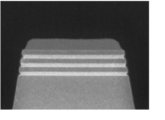
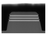
- Figures 11 and 12 are SEM images of the substrate after the etching process of evaluation test 2-1, and Figure 12 is an enlarged portion of the image in Figure 11. As these images show, the central portion of the side of each SiGe film in the stacking direction of each film (thickness direction of the substrate) was etched more than the other portions, and the rectangularity described above was not high. Furthermore, the amount of etching of the second-stage SiGe film was less than the amount of etching of the first and third-stage SiGe films.
- Figures 13 and 14 are SEM images of the substrate after the etching process of evaluation test 2-2, and Figure 14 is an enlarged portion of the image in Figure 13. As shown in these images, the side surfaces of each SiGe film are relatively flat, and therefore the rectangularity described above is good. Furthermore, the etching amounts of the first to third SiGe films were roughly uniform. The standardized value of the average etching amount was 1.04. Regarding the variation in the calculated etching amount, the standardized value of 3 ⁇ (unit: nm) was 0.3, and 3 ⁇ % was 27.5%.
- evaluation test 2-2 suppressed the variation in the etching amount within the same SiGe film and between SiGe films of different heights. It was also shown that evaluation test 2-2 had a higher rectangularity of the space formed by etching, and that evaluation test 2-2 suppressed the loading (difference in etching rate) between the film formed on the upper side of the substrate (top) and the film formed on the lower side of the substrate (bottom).
Landscapes
- Physics & Mathematics (AREA)
- Engineering & Computer Science (AREA)
- Plasma & Fusion (AREA)
- Chemical & Material Sciences (AREA)
- Analytical Chemistry (AREA)
- Drying Of Semiconductors (AREA)
- ing And Chemical Polishing (AREA)
Abstract
Description
一実施形態に係るエッチング方法においては、最初に、表面部分にSiGeまたはGeを有する基板を、エッチング処理を行うためのチャンバー内に設ける。次いで、SiGeまたはGeをエッチングするためのエッチングガスを、エッチング反応が生じない第1の温度に保持された基板に供給して、基板の表面に吸着させる。次いで、基板の温度をSiGeまたはGeとエッチングガスとの反応が生じる第2の温度にしてSiGeまたはGeをエッチングする。エッチングガスを基板の表面に吸着させることと、エッチングすることとは複数回繰り返してもよい。
SiGeのSiおよびGeの割合は任意であるが、Siが90at%以下であることが好ましい。また、SiGe、Geの形態は特に限定されないが、膜として形成されたものが例示され、膜としては化学蒸着(CVD)法で形成されたものが例示される。基板は特に限定されないが、半導体ウエハ(以下単にウエハと記す)が例示される。
図6は、一実施形態のエッチング方法が適用される基板であるウエハの構造例を示す断面図である。図6のウエハWは、例えばSiからなる半導体基体100の表面に、SiGe膜111と、Si膜112とが交互に積層された積層構造部113を有している。積層構造部113にはプラズマエッチングにより凹部114が形成されており、凹部114には交互に積層されたSiGe膜111とSi膜112の側面が露出している。
次に、実施形態に係るエッチング方法を実施するためのエッチング装置の一例について説明する。図9は、エッチング装置の一例を示す断面図である。
図9に示すように、エッチング装置1は、密閉構造のチャンバー10を備えている。チャンバー10の内部には、基板Wを水平状態で載置する載置台12が設けられている。基板Wは表面にSiGeまたはGeを有するものであり、例えば、図6の構造を有している。また、エッチング装置1は、チャンバー10にエッチングガスを供給するガス供給機構13、チャンバー10内を排気する排気機構14、および制御部15を備えている。
ところでエッチング装置の他の例であるエッチング装置1Aについて以下に述べる。エッチング装置1Aは、ステップST2、ST3を実施する第1モジュールと、ステップST4、ST5を実施する第2モジュールと、を備える。第1モジュールはエッチング装置1と同様の構成であり、第2モジュールは、エッチングガスの供給が行われないことを除いてエッチング装置1と同様の構成である。従ってエッチング装置1Aは、基板Wを第1の温度で処理するチャンバー10と、基板Wを第2の温度で処理するチャンバー10と、を個別に備える。
例えばエッチングガスを第1の温度の基板Wに吸着させるステップST2を行った後、パージや排気によって基板Wの表面から当該表面に吸着されていない余分なエッチングガスを除去するステップST3が行われずに、ステップST4の基板Wを第2の温度にすることでのエッチングが行われてもよい。チャンバー10に供給するエッチングガスの供給量については、例えばエッチング対象のSiGe膜表面への吸着が飽和し、且つ表面の各部での吸着量のばらつきが抑えられるように、事前に実験等を行うなどして、適量となるように決めておく。ただし吸着量のばらつきがより確実に抑えられるようにしてSiGe膜表面の各部でエッチング量がばらつくことを抑えるために、ステップST3を行うことが有効である。
以上、実施形態について説明したが、今回開示された実施形態は、全ての点で例示であって制限的なものではないと考えられるべきである。上記の実施形態は、添付の特許請求の範囲およびその主旨を逸脱することなく、様々な形態で省略、置換、変更されてもよい。
以下、本開示におけるエッチング方法に関して行われた評価試験について説明する。
評価試験1として、平坦な表面にSiGe膜が形成された複数のウエハに対して、エッチング装置1Aを用いて本開示のエッチング処理を行い、当該SiGe膜のエッチング量を測定した。エッチング処理については、ウエハ毎にステップST2~ST5のサイクルを実施する回数(以下、サイクル数と記載する)及びステップST2の実施時間(即ち、エッチングガスの供給時間)の組み合わせを変更して行った。
評価試験2では、図6に示すような表面部分にSiGe膜とSi膜とが交互に設けられた積層部が形成された基板を用意して試験を行った。この積層部においてSiGe膜は互いに離れて3段に形成されており、各段のSiGe膜の上側及び下側はSi膜に接している。そして、各SiGe膜の側面は概ね平坦であると共に、基板の面方向に対して概ね垂直に形成されている。このような基板に対し、本開示のエッチング処理と、後述する比較例のエッチング処理とを行い、エッチング処理の前後で取得したSEM画像を比較した。詳しく述べるとSEM画像より、SiGe膜間におけるエッチングの違い、各段のSiGe膜のエッチングによって形成される凹部の矩形性について検証した。さらに、各SiGe膜における異なる高さ位置の横方向のエッチング量を測定し、ばらつきを算出した。
10;チャンバー
12;載置台
13;ガス供給機構
14;排気機構
26;シャワーヘッド
35;温調機構
100;半導体基体
101,111;SiGe膜
102;エッチングガス
112;Si膜
114;凹部
W;半導体ウエハ(基板)
Claims (15)
- 表面部分にSiGeまたはGeを有する基板をチャンバー内に設けることと、
SiGeまたはGeをエッチングするためのエッチングガスを、エッチング反応が生じない第1の温度に保持された前記基板に供給して、基板の表面に吸着させることと、
前記基板の温度を前記SiGeまたはGeと前記エッチングガスとの反応が生じる第2の温度にして前記SiGeまたはGeをエッチングすることと、
を有する、エッチング方法。 - 前記エッチングガスを前記基板の表面に吸着させることと、前記エッチングすることと、を複数回繰り返す、請求項1に記載のエッチング方法。
- 前記エッチングガスを前記基板の表面に吸着させることの後に、前記エッチングガスを前記チャンバーから排出させることをさらに有する、請求項1に記載のエッチング方法。
- 前記エッチングガスを前記チャンバーから排出させることは、前記チャンバー内を不活性ガスでパージすることにより行われる、請求項3に記載のエッチング方法。
- 前記エッチングすることの後に、前記エッチングすることにより生じた残留物を前記チャンバーから排出させることをさらに有する、請求項1に記載のエッチング方法。
- 前記残留物を前記チャンバーから排出させることは、前記チャンバー内を真空引きすることにより行う、請求項5に記載のエッチング方法。
- 前記基板は、処理中にエッチングガスが接触する部分にSiが存在し、前記SiGeまたはGeを前記Siに対して選択的にエッチングする、請求項1から請求項6のいずれか一項に記載のエッチング方法。
- 前記SiGeまたはGeが、SiGe膜またはGe膜であり、前記SiがSi膜である、請求項7に記載のエッチング方法。
- 前記基板は、表面部分に前記SiGe膜と前記Si膜とが交互に積層されてなる積層構造部を有する、請求項8に記載のエッチング方法。
- 前記エッチングガスは、フッ素含有ガスである、請求項7に記載のエッチング方法。
- 前記フッ素含有ガスは、ClF3ガス、F2ガス、SF6ガス、IF7ガスの少なくとも一種である、請求項10に記載のエッチング方法。
- 前記エッチングガスとしてフッ素含有ガスを用いる場合に、前記第1の温度は-20℃以下であり、前記第2の温度は前記第1の温度よりも高い請求項10に記載のエッチング方法。
- 前記第2の温度は常温以下である請求項12に記載のエッチング方法。
- 前記エッチングガスを前記基板の表面に吸着させる際に、前記基板に前記エッチングガスとともに不活性ガスを供給する、請求項1に記載のエッチング方法。
- 表面部分にSiGeまたはGeを有する基板を収容するチャンバーと、
前記チャンバー内で基板を載置する載置台と、
前記チャンバー内にエッチングガスを供給するガス供給部と、
前記チャンバー内を排気する排気部と、
前記載置台上の基板の温度を調節する温調機構と、
制御部と、
を具備し、
前記制御部は、前記請求項1から請求項14のいずれか一項のエッチング方法が行われるように、前記ガス供給部と、前記排気部と、前記温調部とを制御する、エッチング装置。
Priority Applications (2)
| Application Number | Priority Date | Filing Date | Title |
|---|---|---|---|
| KR1020267009959A KR20260059656A (ko) | 2023-09-11 | 2024-08-28 | 에칭 방법 및 에칭 장치 |
| US19/562,917 US20260206508A1 (en) | 2023-09-11 | 2026-03-11 | Etching Method and Etching Apparatus |
Applications Claiming Priority (2)
| Application Number | Priority Date | Filing Date | Title |
|---|---|---|---|
| JP2023147055A JP2025040250A (ja) | 2023-09-11 | 2023-09-11 | エッチング方法およびエッチング装置 |
| JP2023-147055 | 2023-09-11 |
Related Child Applications (1)
| Application Number | Title | Priority Date | Filing Date |
|---|---|---|---|
| US19/562,917 Continuation US20260206508A1 (en) | 2023-09-11 | 2026-03-11 | Etching Method and Etching Apparatus |
Publications (1)
| Publication Number | Publication Date |
|---|---|
| WO2025057740A1 true WO2025057740A1 (ja) | 2025-03-20 |
Family
ID=95022194
Family Applications (1)
| Application Number | Title | Priority Date | Filing Date |
|---|---|---|---|
| PCT/JP2024/030794 Ceased WO2025057740A1 (ja) | 2023-09-11 | 2024-08-28 | エッチング方法およびエッチング装置 |
Country Status (5)
| Country | Link |
|---|---|
| US (1) | US20260206508A1 (ja) |
| JP (1) | JP2025040250A (ja) |
| KR (1) | KR20260059656A (ja) |
| TW (1) | TW202516620A (ja) |
| WO (1) | WO2025057740A1 (ja) |
Citations (3)
| Publication number | Priority date | Publication date | Assignee | Title |
|---|---|---|---|---|
| JP2005064035A (ja) * | 2003-08-12 | 2005-03-10 | Fujio Masuoka | 半導体装置のエッチング法 |
| JP2020021958A (ja) * | 2019-10-30 | 2020-02-06 | 東京エレクトロン株式会社 | 基板処理装置および基板載置台 |
| JP2020053448A (ja) * | 2018-09-25 | 2020-04-02 | 東京エレクトロン株式会社 | エッチング方法、エッチング装置、および記憶媒体 |
-
2023
- 2023-09-11 JP JP2023147055A patent/JP2025040250A/ja active Pending
-
2024
- 2024-08-28 WO PCT/JP2024/030794 patent/WO2025057740A1/ja not_active Ceased
- 2024-08-28 KR KR1020267009959A patent/KR20260059656A/ko active Pending
- 2024-09-02 TW TW113133032A patent/TW202516620A/zh unknown
-
2026
- 2026-03-11 US US19/562,917 patent/US20260206508A1/en active Pending
Patent Citations (3)
| Publication number | Priority date | Publication date | Assignee | Title |
|---|---|---|---|---|
| JP2005064035A (ja) * | 2003-08-12 | 2005-03-10 | Fujio Masuoka | 半導体装置のエッチング法 |
| JP2020053448A (ja) * | 2018-09-25 | 2020-04-02 | 東京エレクトロン株式会社 | エッチング方法、エッチング装置、および記憶媒体 |
| JP2020021958A (ja) * | 2019-10-30 | 2020-02-06 | 東京エレクトロン株式会社 | 基板処理装置および基板載置台 |
Also Published As
| Publication number | Publication date |
|---|---|
| US20260206508A1 (en) | 2026-07-16 |
| JP2025040250A (ja) | 2025-03-24 |
| KR20260059656A (ko) | 2026-04-30 |
| TW202516620A (zh) | 2025-04-16 |
Similar Documents
| Publication | Publication Date | Title |
|---|---|---|
| CN110581067B (zh) | 蚀刻方法及蚀刻装置 | |
| US11594417B2 (en) | Etching method and apparatus | |
| US20200098575A1 (en) | Etching Method, Etching Apparatus, and Storage Medium | |
| US8535479B2 (en) | Manufacturing method of semiconductor device, and semiconductor device | |
| CN108352309B (zh) | 基板处理方法和基板处理装置 | |
| TWI675420B (zh) | 蝕刻方法 | |
| US20160056035A1 (en) | Method of Manufacturing Semiconductor Device | |
| US11011383B2 (en) | Etching method | |
| US10312079B2 (en) | Etching method | |
| US11557486B2 (en) | Etching method, damage layer removal method, and storage medium | |
| US10923358B2 (en) | Substrate processing method | |
| US12628586B2 (en) | Etching method including steps of an oxidation process, a gas based chemical process, and removal of chemical products | |
| US10622205B2 (en) | Substrate processing method and substrate processing apparatus | |
| WO2012018010A1 (ja) | 基板処理方法および基板処理装置 | |
| US20240006187A1 (en) | Etching method and etching apparatus | |
| JP2020025070A (ja) | エッチング方法およびエッチング装置 | |
| US9236272B2 (en) | Etching apparatus and etching method | |
| TWI791741B (zh) | 蝕刻方法 | |
| WO2015186461A1 (ja) | エッチング方法 | |
| JP7738439B2 (ja) | エッチング方法およびエッチング装置 | |
| JP7486398B2 (ja) | エッチング方法およびエッチング装置 | |
| JP7521230B2 (ja) | エッチング方法及びエッチング装置 | |
| JP2025040250A (ja) | エッチング方法およびエッチング装置 | |
| KR102608729B1 (ko) | 에칭 방법 및 에칭 장치 | |
| JP7822166B2 (ja) | ガス処理方法およびガス処理装置 |
Legal Events
| Date | Code | Title | Description |
|---|---|---|---|
| 121 | Ep: the epo has been informed by wipo that ep was designated in this application |
Ref document number: 24865242 Country of ref document: EP Kind code of ref document: A1 |
|
| ENP | Entry into the national phase |
Ref document number: 1020267009959 Country of ref document: KR Free format text: ST27 STATUS EVENT CODE: A-0-1-A10-A15-NAP-PA0105 (AS PROVIDED BY THE NATIONAL OFFICE) |
|
| NENP | Non-entry into the national phase |
Ref country code: DE |
|
| WWE | Wipo information: entry into national phase |
Ref document number: 11202601453P Country of ref document: SG |
|
| WWP | Wipo information: published in national office |
Ref document number: 11202601453P Country of ref document: SG |