WO2025052753A1 - 赤外線ヒーター - Google Patents
赤外線ヒーター Download PDFInfo
- Publication number
- WO2025052753A1 WO2025052753A1 PCT/JP2024/021525 JP2024021525W WO2025052753A1 WO 2025052753 A1 WO2025052753 A1 WO 2025052753A1 JP 2024021525 W JP2024021525 W JP 2024021525W WO 2025052753 A1 WO2025052753 A1 WO 2025052753A1
- Authority
- WO
- WIPO (PCT)
- Prior art keywords
- layer
- conductor
- adhesive layer
- infrared heater
- dielectric layer
- Prior art date
- Legal status (The legal status is an assumption and is not a legal conclusion. Google has not performed a legal analysis and makes no representation as to the accuracy of the status listed.)
- Pending
Links
Images






Classifications
-
- H—ELECTRICITY
- H05—ELECTRIC TECHNIQUES NOT OTHERWISE PROVIDED FOR
- H05B—ELECTRIC HEATING; ELECTRIC LIGHT SOURCES NOT OTHERWISE PROVIDED FOR; CIRCUIT ARRANGEMENTS FOR ELECTRIC LIGHT SOURCES, IN GENERAL
- H05B3/00—Ohmic-resistance heating
- H05B3/20—Heating elements having extended surface area substantially in a two-dimensional [2D] plane, e.g. plate-heater
- H05B3/22—Heating elements having extended surface area substantially in a two-dimensional [2D] plane, e.g. plate-heater non-flexible
- H05B3/26—Heating elements having extended surface area substantially in a two-dimensional [2D] plane, e.g. plate-heater non-flexible heating conductor mounted on insulating base
-
- H—ELECTRICITY
- H05—ELECTRIC TECHNIQUES NOT OTHERWISE PROVIDED FOR
- H05B—ELECTRIC HEATING; ELECTRIC LIGHT SOURCES NOT OTHERWISE PROVIDED FOR; CIRCUIT ARRANGEMENTS FOR ELECTRIC LIGHT SOURCES, IN GENERAL
- H05B3/00—Ohmic-resistance heating
- H05B3/10—Heating elements characterised by the composition or nature of the materials or by the arrangement of the conductor
-
- H—ELECTRICITY
- H05—ELECTRIC TECHNIQUES NOT OTHERWISE PROVIDED FOR
- H05B—ELECTRIC HEATING; ELECTRIC LIGHT SOURCES NOT OTHERWISE PROVIDED FOR; CIRCUIT ARRANGEMENTS FOR ELECTRIC LIGHT SOURCES, IN GENERAL
- H05B3/00—Ohmic-resistance heating
- H05B3/20—Heating elements having extended surface area substantially in a two-dimensional [2D] plane, e.g. plate-heater
-
- H—ELECTRICITY
- H05—ELECTRIC TECHNIQUES NOT OTHERWISE PROVIDED FOR
- H05B—ELECTRIC HEATING; ELECTRIC LIGHT SOURCES NOT OTHERWISE PROVIDED FOR; CIRCUIT ARRANGEMENTS FOR ELECTRIC LIGHT SOURCES, IN GENERAL
- H05B2203/00—Aspects relating to Ohmic resistive heating covered by group H05B3/00
- H05B2203/013—Heaters using resistive films or coatings
-
- H—ELECTRICITY
- H05—ELECTRIC TECHNIQUES NOT OTHERWISE PROVIDED FOR
- H05B—ELECTRIC HEATING; ELECTRIC LIGHT SOURCES NOT OTHERWISE PROVIDED FOR; CIRCUIT ARRANGEMENTS FOR ELECTRIC LIGHT SOURCES, IN GENERAL
- H05B2203/00—Aspects relating to Ohmic resistive heating covered by group H05B3/00
- H05B2203/032—Heaters specially adapted for heating by radiation heating
Definitions
- the present invention relates to an infrared heater.
- an infrared heater that emit infrared rays.
- an infrared heater has been proposed that includes a heating element and a structure having an infrared radiation surface, and the structure includes a first conductor layer including a plurality of individual conductor layers that form a periodic structure, an adhesive layer, a dielectric layer, and a second conductor layer in this order (see, for example, Patent Document 1).
- infrared heater when the structure absorbs energy from the heating element, infrared rays having a half-width of 1.5 ⁇ m or less and a maximum peak with an emissivity of 0.8 or more are emitted.
- a higher temperature e.g. 400° C. or higher
- the heat resistance of infrared heaters will be improved so that they can operate in high temperature ranges.
- the main objective of the present invention is to provide an infrared heater with excellent heat resistance.
- An infrared heater includes a dielectric layer, a conductor pattern including a plurality of first conductor parts, and a second conductor part.
- the conductor pattern is disposed on the dielectric layer.
- the plurality of first conductor parts are arranged at intervals from each other to form a periodic structure.
- the second conductor part is disposed on the opposite side of the dielectric layer to the conductor pattern.
- Each of the plurality of first conductor parts includes a first adhesive layer, a first barrier layer, and a first body layer.
- the first adhesive layer is in contact with the dielectric layer.
- the first body layer is disposed on the opposite side of the first adhesive layer to the dielectric layer.
- the first barrier layer is disposed between the first adhesive layer and the first body layer.
- the first barrier layer is capable of blocking migration of a material constituting the first adhesive layer to the first body layer.
- the first barrier layer may have a thickness of 0.2 nm or more and 50 nm or less.
- the material constituting the first barrier layer may contain a platinum group element and/or an oxide thereof.
- the second conductor may include a second adhesive layer, a second barrier layer, and a second body layer. The second adhesive layer is in contact with the dielectric layer.
- the second body layer is disposed on the opposite side of the second adhesive layer to the dielectric layer.
- the second barrier layer is disposed between the second adhesive layer and the second body layer.
- the second barrier layer is capable of preventing migration of a material constituting the second adhesive layer to the second body layer.
- the infrared heater according to the above [4] may further include a support substrate.
- the support substrate is disposed on the opposite side of the second conductor portion to the dielectric layer.
- the second conductor may further include a third adhesive layer and a third barrier layer.
- the third adhesive layer is in contact with the support substrate.
- the third barrier layer is disposed between the third adhesive layer and the second main body layer.
- the third barrier layer can prevent a material constituting the third adhesive layer from migrating to the second main body layer.
- the thickness of each of the first conductors may be 30 nm or more and 200 nm or less.
- the length of one side of the first conductor may be 500 nm or more and 8000 nm or less.
- the diameter of the first conductor may be 500 nm or more and 8000 nm or less.
- a distance between adjacent first conductors among the plurality of first conductors may be 300 nm or more and 4000 nm or less.
- the infrared heater according to any one of the above [1] to [8] may further include a heating unit capable of heating a metamaterial structure including the dielectric layer, the plurality of first conductors, and the second conductor.
- the metamaterial structure may be configured such that a resonance phenomenon due to magnetic polaritons occurs when the heating unit is heated.
- the infrared heater may be capable of emitting infrared rays having a maximum peak with a normal emissivity of 0.8 or more.
- the peak wavelength of the maximum peak may be 2 ⁇ m or more and 10 ⁇ m or less, and the half width of the maximum peak may be 1.5 ⁇ m or less.
- an infrared heater with excellent heat resistance can be realized.
- FIG. 1 is a schematic cross-sectional view of an infrared heater according to one embodiment of the present invention.
- FIG. 2 is a cross-sectional view of the first conductor portion shown in FIG. 1 taken along line II-II'.
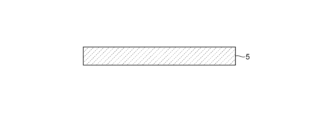
- FIG. 3A is a schematic cross-sectional view illustrating a step of preparing a support substrate in a method for manufacturing an infrared heater according to an embodiment of the present invention.
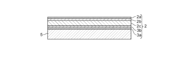
- FIG. 3B is a schematic cross-sectional view for illustrating a step of forming a second conductor on the support substrate of FIG. 3A.
- FIG. 3C is a schematic cross-sectional view for illustrating a step of forming a dielectric layer on the second conductor portion in FIG. 3B.
- FIG. 3A is a schematic cross-sectional view of preparing a support substrate in a method for manufacturing an infrared heater according to an embodiment of the present invention.
- FIG. 3B is a schematic cross-sectional view for illustrating a step of
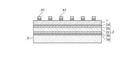
- FIG. 3D is a schematic cross-sectional view for illustrating a step of forming a resist pattern on the dielectric layer of FIG. 3C.
- FIG. 3E is a schematic cross-sectional view for illustrating a step of forming a conductor pattern on the dielectric layer via the resist pattern of FIG. 3D.
- FIG. 4 is a graph showing infrared emissivity curves of the infrared heater of Example 2 before and after a heating durability test.
- FIG. 5 is a graph showing infrared emissivity curves before and after a heating durability test for the infrared heater of Comparative Example 2.
- FIG. 6 is a graph showing infrared emissivity curves of the infrared heater of Example 2 before and after a heating durability test.
- FIG. 7 is a graph showing infrared emissivity curves before and after a heating durability test for the infrared heater of Example 3.
- FIG. 8 is a graph showing infrared emissivity curves before and after a heating durability test for the infrared heater of Example 4.
- FIG. 9 is a scanning electron microscope (SEM) photograph of the first conductor portion of the infrared heater of Example 2 before the heating durability test.
- FIG. 10 is a SEM photograph of the first conductor of the infrared heater of Example 2 after a 500-hour heating durability test.
- FIG. 11 is a SEM photograph of the first conductor of the infrared heater of Example 3 after a 500-hour heating durability test.
- FIG. 12 is a SEM photograph of the first conductor of the infrared heater of Example 4 after a 500-hour heating durability test.
- FIG. 1 is a schematic cross-sectional view of an infrared heater according to one embodiment of the present invention
- Fig. 2 is a cross-sectional view of the first conductor portion taken along line II-II' in Fig. 1. For convenience, hatching has been omitted in Fig. 2.
- the illustrated infrared heater 100 can emit infrared rays with a controlled wavelength, more specifically, infrared rays with a controlled wavelength (hereinafter, referred to as peak wavelength) at which the normal emissivity is maximized. That is, the infrared heater 100 typically functions as a wavelength-controlled heater.
- the infrared heater 100 includes a dielectric layer 1, a conductor pattern 4 including a plurality of first conductor portions 41, and a second conductor portion 2.
- the conductor pattern 4 is disposed on the dielectric layer 1.
- the plurality of first conductor portions 41 are arranged at intervals to form a periodic structure.
- the second conductor portion 2 is disposed on the opposite side of the dielectric layer 1 to the conductor pattern 4.
- Each of the multiple first conductor parts 41 includes a first adhesive layer 41a, a first barrier layer 41b, and a first body layer 41c.
- the first adhesive layer 41a is in contact with the dielectric layer 1.
- the first body layer 41c is disposed on the opposite side of the first adhesive layer 41a to the dielectric layer 1.
- the first barrier layer 41b is disposed between the first adhesive layer 41a and the first body layer 41c.
- the first barrier layer 41b can prevent the material constituting the first adhesive layer 41a from migrating to the first body layer 41c.
- the present inventors have discovered that when an infrared heater is operated in a high temperature range (e.g., 400°C or higher), the maximum emissivity of infrared rays emitted by the infrared heater gradually decreases.
- the heat resistance of an infrared heater can be sufficiently improved by providing a first barrier layer between the first adhesive layer and the first main body layer in the first conductor. More specifically, when a first barrier layer is provided between the first adhesive layer and the first main body layer, the first barrier layer can suppress the migration of the material constituting the first adhesive layer to the first main body layer. This can suppress the material of the first adhesive layer from migrating to the first main body layer and forming an oxide film on the first main body layer even when the infrared heater is operated in a high temperature range.
- the infrared heater can be operated in a high temperature range for a long period of time and can stably emit infrared rays with excellent maximum normal emissivity.
- Such an infrared heater 100 can be suitably operated in a temperature range of, for example, 10°C or higher and 600°C or lower, for example, 650°C or higher and 800°C or lower, or for example, 400°C or higher and 1000°C or lower.
- the multiple first conductors 41, the dielectric layer 1, and the second conductors 2 form a metamaterial structure 10.
- the metamaterial structure 10 is typically configured to generate a resonance phenomenon caused by magnetic polaritons. When this resonance phenomenon occurs, a strong electromagnetic field confinement effect can occur in the dielectric layer 1 between the multiple first conductors 41 and the second conductors 2. This causes the portions of the dielectric layer 1 sandwiched between the first conductors 41 and the second conductors 2 to function as an infrared radiation source.
- infrared rays with a controlled peak wavelength are radiated from a portion of the surface of the dielectric layer 1 where the multiple first conductors 41 are not provided (hereinafter referred to as the radiation surface 1a), going around the multiple first conductors 41.
- the infrared heater 100 can emit infrared rays having a maximum peak normal emissivity of 0.80 or more.
- the maximum peak can be determined, for example, from an infrared emissivity curve (see FIG. 4) that is determined by plotting the wavelength of infrared rays and the normal emissivity.
- the peak wavelength of the maximum peak is located, for example, in the range of 2.0 ⁇ m or more and 10 ⁇ m or less, and is also located, for example, in the range of 3.0 ⁇ m or more and 7.0 ⁇ m or less.
- the maximum peak normal emissivity is preferably 0.85 or more, more preferably 0.90 or more.
- the upper limit of the maximum peak normal emissivity is typically 1.0.
- the normal emissivity in infrared rays is calculated, for example, by the following formula (1) obtained by applying Kirchhoff's law with the transmittance set to a value of 0.
- the normal reflectivity is measured, for example, by a Fourier transform infrared spectrometer (FT-IR) having an integrating sphere.
- FT-IR Fourier transform infrared spectrometer
- Vertical emissivity 1 - (vertical reflectance)...(1)
- the half width of the maximum peak is, for example, 1.5 ⁇ m or less, and preferably 1.0 ⁇ m or less, whereas the lower limit of the half width of the maximum peak is typically 0 ⁇ m.
- the second conductor portion 2 includes a second adhesive layer 2a, a second barrier layer 2b, and a second body layer 2c.
- the second adhesive layer 2a is in contact with the dielectric layer 1.
- the second body layer 2c is disposed on the opposite side of the second adhesive layer 2a to the dielectric layer 1.
- the second barrier layer 2b is disposed between the second adhesive layer 2a and the second body layer 2c.
- the second barrier layer 2b can prevent the material constituting the second adhesive layer 2a from migrating to the second body layer 2c. According to this configuration, since both the first conductor and the second conductor have a laminated structure, the above-mentioned resonance phenomenon can be stably generated in the metamaterial structure.
- the second barrier layer can suppress the migration of the material constituting the second adhesive layer to the second main body layer. Therefore, the heat resistance of the infrared heater can be further improved, and the infrared heater can radiate infrared rays having the above-mentioned maximum peak more stably.
- the infrared heater 100 further includes a support substrate 5.
- the support substrate 5 is disposed on the opposite side of the second conductor portion 2 from the dielectric layer 1. This allows the support substrate to stably support the metamaterial structure described above.
- the second conductor 2 further includes a third adhesive layer 3a and a third barrier layer 3b.
- the third adhesive layer 3a is in contact with the support substrate 5.
- the third barrier layer 3b is disposed between the third adhesive layer 3a and the second body layer 2c.
- the third barrier layer 3b can prevent the material constituting the third adhesive layer 3a from migrating to the second body layer 2c.
- the infrared heater 100 further includes a heating unit 6.
- the heating unit 6 is capable of heating the metamaterial structure 10.
- the above-mentioned resonance phenomenon can occur due to heating by the heating unit 6. This allows the infrared heater to stably radiate the above-mentioned infrared rays.
- the heating section 6 is disposed on the opposite side of the supporting substrate 5 to the second conductor section 2. Therefore, the heating section can smoothly heat the metamaterial structure via the supporting substrate.
- the infrared heater 100 has any suitable shape when viewed from the thickness direction of the dielectric layer 1.
- shapes of the infrared heater when viewed from the thickness direction include a triangle, a rectangle, a pentagon, a polygon with hexagons or more, a circle, and an ellipse.
- the dielectric layer 1 is disposed between the conductor pattern 4 including a plurality of first conductor portions 41 and the second conductor portion 2. In the illustrated example, the dielectric layer 1 is in direct contact with each of the first conductor portion 41 and the second conductor portion 2.
- the material constituting the dielectric layer 1 may be any suitable inorganic oxide capable of forming a metamaterial structure.
- the inorganic oxide include silica (SiO 2 ) and alumina (Al 2 O 3 ), and preferably alumina.
- the inorganic oxide may be used alone or in combination.
- the thickness d of the dielectric layer 1 is, for example, 30 nm or more, preferably 100 nm or more, and more preferably 150 nm or more.
- the thickness d of the dielectric layer 1 is, for example, 300 nm or less, preferably 250 nm or less, and more preferably 210 nm or less.
- Conductive pattern including a plurality of first conductor portions The conductor pattern 4 is typically provided directly on the surface of the dielectric layer 1 opposite to the second conductor portion 2.
- the conductor pattern 4 has any appropriate pattern shape capable of forming a metamaterial structure.
- the conductor pattern 4 includes a plurality of first conductor portions 41. Each of the plurality of first conductor portions 41 typically has electrical conductivity.
- the first conductor parts 41 are arranged at equal intervals on the dielectric layer 1 to form a periodic structure. More specifically, a row of the first conductor parts 41 arranged at equal intervals in the first plane direction of the dielectric layer 1 is arranged in parallel at equal intervals in the second plane direction perpendicular to the first plane direction (see FIG. 2).
- the interval between adjacent first conductors 41 among the plurality of first conductors 41 is, for example, 300 nm or more, for example, 500 nm or more, or for example, 1000 nm or more.
- the interval between adjacent first conductors 41 is, for example, 8000 nm or less, for example, 5000 nm or less, or for example, 4000 nm or less.
- Each of the first conductors 41 may have any appropriate shape capable of forming a metamaterial structure.
- Examples of the shape of the first conductors 41 as viewed in the thickness direction include a circular shape and a rectangular shape (quadangle shape), preferably a rectangular shape, and more preferably a square shape.
- the dimension of the first conductor 41 in the plane direction (first plane direction or second plane direction) of the dielectric layer can be arbitrarily and appropriately adjusted according to the desired peak wavelength.
- the length (width) w of one side of the first conductor 41 is, for example, 500 nm or more, or, for example, 1000 nm or more.
- the length (width) w of one side of the first conductor 41 is, for example, 8000 nm or less, or, for example, 4000 nm or less.
- the range of the diameter (width) of the first conductor portion 41 is, for example, the same as the range of the width w described above.
- the shapes and sizes of the first conductors 41 may all be the same, or at least some of them may differ from one another.
- the shapes and sizes of the first conductors 41 are preferably all the same.
- the period ⁇ of the periodic structure formed by the multiple first conductors 41 is the sum of the interval between the adjacent first conductors 41 and the width w of the first conductors 41.
- the period ⁇ can be arbitrarily and appropriately adjusted according to the desired peak wavelength.
- the period ⁇ is, for example, 500 nm or more, or, for example, 1000 nm or more.
- the period ⁇ is, for example, 8000 nm or less, or, for example, 4000 nm or less. If the period ⁇ is within this range, the angle dependency of the infrared heater can be suitably adjusted.
- the thickness h of the first conductor portion 41 is, for example, 30 nm or more, and preferably 50 nm or more. On the other hand, the thickness h of the first conductor portion 41 is, for example, 200 nm or less, preferably 150 nm or less, and more preferably 100 nm or less. When the thickness of the first conductor portion is in this range, the peak wavelength of the infrared light can be stably adjusted to the above range.
- each of the first conductors 41 includes the first adhesive layer 41a, the first barrier layer 41b, and the first main body layer 41c.
- the first adhesive layer 41a typically bonds the first conductor portion 41 to the dielectric layer 1. This can improve the adhesion of the first conductor portion to the dielectric layer and can suppress peeling of the first conductor portion from the dielectric layer.
- the first adhesive layer 41a may be made of any suitable metal material.
- metal materials constituting the first adhesive layer 41a include chromium (Cr), nickel (Ni), titanium (Ti), and alloys thereof, with titanium (Ti) being preferred.
- the thickness of the first adhesive layer 41a is, for example, 0.2 nm or more, and preferably 3.0 nm or more. If the first adhesive layer has such a thickness, the adhesion of the first conductor portion to the dielectric layer can be stably improved. On the other hand, the thickness of the first adhesive layer 41a is, for example, 30 nm or less, preferably 20 nm or less, more preferably 10 nm or less, and even more preferably 8.0 nm or less.
- the first barrier layer 41b is provided directly on the surface of the first adhesive layer 41a opposite to the dielectric layer 1.
- the first barrier layer 41b is typically provided over the entire surface of the first adhesive layer 41a opposite to the dielectric layer 1. This can provide a more stable barrier against migration of the material of the first adhesive layer to the first body layer.
- the first barrier layer 41b may be made of any suitable metal material.
- the metal material constituting the first barrier layer 41b include platinum group elements and their oxides. Specific examples of platinum group elements include platinum (Pt), palladium (Pd), and ruthenium (Ru), preferably platinum (Pt) and palladium (Pd), and more preferably platinum (Pt).
- the metal material constituting the first barrier layer 41b may be an alloy of two or more platinum group elements.
- the thickness of the first barrier layer 41b is, for example, 0.2 nm or more, more preferably 1.0 nm or more, and even more preferably 3.0 nm or more. If the first barrier layer has such a thickness, migration of the material of the first adhesive layer to the first main body layer can be stably suppressed. On the other hand, the thickness of the first barrier layer 41b is, for example, 50 nm or less, more preferably 30 nm or less, even more preferably 20 nm or less, particularly preferably 15 nm or less, particularly preferably 10 nm or less, and most preferably 8.0 nm or less.
- the first barrier layer has such a thickness, it is possible to suppress the first barrier layer from affecting the resonance phenomenon occurring in the metamaterial structure, and it is possible to more stably radiate infrared rays having the above-mentioned maximum peak. Furthermore, if the thickness of the first barrier layer is not more than this upper limit, grain growth in the first barrier layer can be suppressed even if the infrared heater is exposed to high temperatures for a long period of time. If grain growth occurs in the first barrier layer, the pattern shape of the first conductor may be distorted (deformed), and the maximum emissivity of the infrared rays radiated by the infrared heater may decrease.
- the pattern shape of the first conductor can be prevented from collapsing (deforming) even if the infrared heater is exposed to high temperatures for a long period of time, and the maximum emissivity of the infrared radiation emitted by the infrared heater can be sufficiently suppressed from decreasing, thereby further improving the heat resistance of the infrared heater.
- the thickness of the first barrier layer 41b is typically equal to or greater than the thickness of the first adhesive layer 41a. That is, the thickness ratio of the first barrier layer 41b to the thickness of the first adhesive layer 41a (thickness of the first barrier layer/thickness of the first adhesive layer) is, for example, 1.0 or greater. On the other hand, the thickness of the first barrier layer/thickness of the first adhesive layer is, for example, 10 or less, preferably 5.0 or less, and more preferably 2.0 or less. The thickness of the first barrier layer 41b is typically less than the thickness of the first main layer 41c.
- the thickness ratio of the first barrier layer 41b to the thickness of the first main layer 41c is, for example, 0.02 or more, preferably 0.05 or more.
- the thickness of the first barrier layer/thickness of the first main layer is, for example, 0.50 or less, preferably 0.30 or less, more preferably 0.15 or less.
- first body layer 41c is provided directly on the surface of the first barrier layer 41b opposite to the first adhesive layer 41a.
- the first body layer 41c is typically provided over the entire surface of the first barrier layer 41b opposite to the first adhesive layer 41a.
- the first body layer 41c may be made of any suitable metal material, such as a low-melting-point material having a melting point of less than 2500° C., a high-melting-point material having a melting point of 2500° C. or higher, or an alloy thereof.
- suitable metal material such as a low-melting-point material having a melting point of less than 2500° C., a high-melting-point material having a melting point of 2500° C. or higher, or an alloy thereof.
- low melting point materials include gold (Au, melting point: 1064°C), silver (Ag, melting point: 962°C), copper (Cu, melting point: 1085°C), iron (Fe, melting point: 1538°C), aluminum (Al, melting point: 660°C), and alloys thereof, and preferably gold (Au).
- high melting point materials include iridium (Ir, melting point: 2466°C), ruthenium (Ru, melting point: 2334°C), hafnium nitride (HfN, melting point: 3334°C), titanium nitride (TiN, melting point: 2930°C), and alloys thereof.
- iridium Ir, melting point: 2466°C
- ruthenium Ru, melting point: 2334°C
- hafnium nitride HfN, melting point: 3334°C
- titanium nitride TiN, melting point: 2930°C
- the thickness of the first main body layer 41c is, for example, 30 nm or more and 200 nm or less, and preferably 50 nm or more and 110 nm or less.
- the second conductor section 2 is typically provided directly on the surface of the dielectric layer 1 opposite the conductor pattern 4.
- the second conductor section 2 has electrical conductivity.
- the second conductor section 2 may be provided on the entire surface of the dielectric layer 1 opposite the conductor pattern 4, or may be provided on only a part of that surface. In the illustrated example, the second conductor section 2 is provided in a layer shape across the entire surface of the dielectric layer 1 opposite the conductor pattern 4.
- the second conductor 2 may have a single-layer structure or a laminated structure in which a plurality of metal films are laminated.
- the material constituting the second conductor 2 may be any suitable metal material capable of forming a metamaterial structure.
- the metal material include chromium (Cr), titanium (Ti), ruthenium (Ru), gold (Au), aluminum (Al), nickel (Ni), copper (Cu), silver (Ag), palladium (Pd), and alloys thereof.
- the thickness f of the second conductor 2 is, for example, 30 nm to 500 nm, preferably 50 nm to 300 nm. When the second conductor has such a thickness, the above-mentioned resonance phenomenon can be stably generated in the metamaterial structure.
- the second conductor portion 2 has a laminated structure and includes a second adhesive layer 2a, a second barrier layer 2b, a second main body layer 2c, a third barrier layer 3b, and a third adhesive layer 3a.
- the second adhesive layer 2a typically bonds the second conductor 2 to the dielectric layer 1. This can improve the adhesion of the second conductor to the dielectric layer and suppress peeling of the second conductor from the dielectric layer.
- the second adhesive layer 2a can be described in the same manner as the above-mentioned first adhesive layer 41a. Therefore, the description of the second adhesive layer 2a is omitted.
- the metal material constituting the second adhesive layer 2a is preferably the same as the metal material constituting the first adhesive layer 41a.
- the thickness of the second adhesive layer 2a is preferably the same as the thickness of the first adhesive layer 41a.
- the second barrier layer 2b is provided directly on the surface of the second adhesive layer 2a opposite the dielectric layer 1.
- the second barrier layer 2b is typically provided on the entire surface of the second adhesive layer 2a opposite the dielectric layer 1. This makes it possible to more stably suppress the migration of the material of the second adhesive layer to the second body layer.
- the second barrier layer 2b can be explained in the same manner as the first barrier layer 41b described above. Therefore, the explanation of the second barrier layer 2b is omitted.
- the metal material constituting the second barrier layer 2b is preferably the same as the metal material constituting the first barrier layer 41b.
- the thickness of the second barrier layer 2b is preferably the same as the thickness of the first barrier layer 41b.
- the second body layer 2c is provided directly on the surface of the second barrier layer 2b opposite the second adhesive layer 2a.
- the second body layer 2c is typically provided on the entire surface of the second barrier layer 2b opposite the second adhesive layer 2a.
- the second body layer 2c can be described in the same manner as the first body layer 41c described above. Therefore, the description of the second body layer 2c is omitted.
- the metal material constituting the second body layer 2c is preferably the same as the metal material constituting the first body layer 41c.
- the thickness of the second body layer 2c is preferably the same as the thickness of the first body layer 41c.
- the third adhesive layer 3a is provided directly on the surface of the support substrate 5 facing the second conductor 2.
- the third adhesive layer 3a may be provided on the entire surface of the support substrate 5 facing the second conductor 2, or may be provided on only a part of the surface. In the illustrated example, the third adhesive layer 3a is provided on the entire surface of the support substrate 5.
- the third adhesive layer 3a typically bonds the second conductor 2 to the support substrate 5. This can improve the adhesion of the second conductor to the support substrate, and can suppress the second conductor from peeling off from the support substrate.
- the third adhesive layer 3a can be described in the same manner as the above-mentioned first adhesive layer 41a. Therefore, the description of the third adhesive layer 3a is omitted.
- the metal material constituting the third adhesive layer 3a is preferably the same as the metal material constituting the first adhesive layer 41a.
- the thickness of the third adhesive layer 3a is preferably the same as the thickness of the first adhesive layer 41a.
- the third barrier layer 3b is provided directly on the surface of the third adhesive layer 3a opposite the support substrate 5, and is in contact with the second main body layer 2c.
- the third barrier layer 3b is typically provided on the entire surface of the third adhesive layer 3a opposite the support substrate 5. This makes it possible to more stably suppress the migration of the material of the third adhesive layer to the second main body layer.
- the third barrier layer 3b can be explained in the same manner as the first barrier layer 41b described above. Therefore, the explanation of the third barrier layer 3b is omitted.
- the metal material constituting the third barrier layer 3b is preferably the same as the metal material constituting the first barrier layer 41b.
- the thickness of the third barrier layer 3b is preferably the same as the thickness of the first barrier layer 41b.
- the support substrate 5 can provide excellent mechanical strength to the infrared heater 100. Any appropriate substrate usable for an infrared heater can be adopted as the support substrate 5.
- the support substrate 5 typically has a substantially flat plate shape.
- the material constituting the support substrate 5 may be, for example, a material having excellent heat resistance, such as sapphire, silicon (Si), or quartz, with quartz being preferred.
- the support substrate 5 may have a single-layer structure, or may have a layered structure in which a plurality of substrates are layered.
- the thickness of the support substrate 5 is, for example, not less than 100 ⁇ m and not more than 1000 ⁇ m, and is, for example, not less than 50 ⁇ m and not more than 700 ⁇ m.
- the heating section 6 is typically in contact with the surface of the supporting substrate 5 opposite to the second conductor section 2. As described above, the heating section 6 is capable of heating the metamaterial structure 10.
- the heating temperature of the heating section 6 is, for example, 200° C. or more and 800° C. or less, and preferably 650° C. or more and 800° C. or less. There is no particular limitation on the configuration of the heating section 6. Any appropriate heat generating unit may be adopted as the heating section.
- the heating unit 6 is configured as a sheet heater.
- the heating unit 6 includes a base body 62 and a heating element 61.
- the base 62 is typically made of an insulating material. Examples of the insulating material include insulating resins such as polyimide, and insulating ceramic materials.
- the base 62 has a substantially flat plate shape.
- the heating element 61 is typically embedded in the base 62.
- the heating element 61 is a resistive heating element, and generates heat by receiving power from the outside.
- the heating element 61 includes a heater wire and a terminal.
- the heater wire typically has a linear or strip shape. The heater wire is routed inside the base 62 in an arbitrary and appropriate manner.
- Terminals are provided at both ends of the heater wire.
- the terminals are typically electrically connected to an external power source.
- Examples of materials for the heating element 61 include tungsten (W), molybdenum (Mo), tantalum (Ta), Ta, Fe-Cr-Al alloy, and Ni-Cr alloy.
- FIG. 3A the above-mentioned support substrate 5 is prepared.
- FIG. 3B the above-mentioned second conductor portion 2 is formed on the support substrate 5 as necessary.
- the second conductor portion 2 is formed on the support substrate 5.
- Examples of the film formation method of the second conductor portion 2 include sputtering, plating, and vapor deposition, and preferably sputtering.
- the second conductor portion 2 has a second adhesive layer 2a, a second barrier layer 2b, a second main body layer 2c, a third barrier layer 3b, and a third adhesive layer 3a.
- the above-mentioned film formation method is repeated to form the third adhesive layer 3a, the third barrier layer 3b, the second main body layer 2c, the second barrier layer 2b, and the second adhesive layer 2a in this order from the support substrate 5 side.
- the above-mentioned dielectric layer 1 is formed on the second conductor portion 2.
- the dielectric layer 1 is deposited on the second conductor portion 2.
- the dielectric layer 1 is deposited on the second adhesive layer 2a.
- methods for depositing the dielectric layer 1 include sputtering and atomic layer deposition (ALD).
- a conductor pattern 4 including a plurality of first conductor portions 41 described above is formed on the dielectric layer 1.
- a resist pattern 9 is formed on the dielectric layer 1. Examples of methods for forming the resist pattern 9 include photolithography, nanoimprint lithography, and maskless lithography using electron beam (EB) drawing, and photolithography is preferred. This allows openings corresponding to the multiple first conductors 41 to be formed in the resist pattern 9 with high accuracy. The size of the openings corresponds to the width w of the first conductors 41 described above.
- the above-mentioned multiple first conductors 41 are formed on the exposed portions of the dielectric layer 1 from the resist pattern 9 by any appropriate film formation method.
- the film formation method for the first conductors 41 include sputtering, plating, and vapor deposition, and vapor deposition is preferred. More specifically, the above-mentioned film formation method is repeated to form the first adhesive layer 41a, the first barrier layer 41b, and the first main body layer 41c in this order from the dielectric layer 1 side.
- the resist pattern 9 is then removed by any appropriate method.
- an infrared heater 100 is manufactured, which has a structure of a conductor pattern 4 including a plurality of first conductor portions 41/dielectric layer 1/second conductor portion 2/support substrate 5, as shown in FIG. 1.
- a quartz wafer with a thickness of 625 ⁇ m was prepared as a support substrate.
- a third adhesive layer, a third barrier layer, a second main body layer, a second barrier layer, and a second adhesive layer were formed in this order on the support substrate by sputtering. This resulted in the formation of a second conductor portion including the second adhesive layer, the second barrier layer, the second main body layer, the third barrier layer, and the third adhesive layer.
- the metal materials constituting each of the second adhesive layer, the second barrier layer, the second main body layer, the third barrier layer, and the third adhesive layer, and the thicknesses of each layer are shown in Table 1.
- a dielectric layer made of alumina (Al 2 O 3 ) was formed on the second adhesive layer by sputtering.
- the thickness of the dielectric layer is shown in Table 1.
- a resist pattern was formed on the dielectric layer by photolithography.
- the resist pattern had openings corresponding to the first conductor portions of the conductor pattern.
- a first adhesive layer, a first barrier layer, and a first main layer were formed in this order on the portion of the dielectric layer that was exposed from the resist pattern, thereby forming a conductor pattern on the dielectric layer.
- the conductor pattern included a plurality of first conductors forming a periodic structure.
- Each of the first conductors included a first main body layer, a first barrier layer, and a first adhesive layer.
- the metal materials constituting the first main body layer, the first barrier layer, and the first adhesive layer, and the thicknesses of each layer are shown in Table 1.
- Each of the first conductors had a circular shape when viewed in the thickness direction.
- the diameter of each of the first conductors was 2.3 ⁇ m.
- the period of the first conductors was 4.3 ⁇ m. Thereafter, the resist pattern was removed.
- an infrared heater was obtained that had a structure of a conductor pattern including multiple first conductor parts/dielectric layer/second conductor part/support substrate.
- ⁇ Heat durability test>> The obtained infrared heater was subjected to a heating durability test. More specifically, the infrared heater was placed in a heating furnace and left to stand at 650°C for the time shown in Table 1.
- “0 hr” in Table 1 means the start of the heating durability test (i.e., before heating).
- 10 hr x 5" in Table 1 means that the infrared heater was placed in a heating furnace, heated at 650°C for 10 hours, and then removed from the heating furnace and cooled to room temperature (23°C), and this cycle was repeated five times.
- the infrared heater after the heating durability test shown in Table 1 was allowed to emit infrared rays from the radiation surface of the dielectric layer at room temperature.
- the normal incidence hemispherical reflectance of the infrared rays was measured in the wavelength range of 2.0 ⁇ m to 12.0 ⁇ m using a Fourier transform infrared spectrometer (FT-IR) having an integrating sphere, and the normal emissivity was calculated using the above formula (1).
- the maximum normal emissivity of infrared rays is shown in Table 1.
- the infrared emissivity curve at "0 hr" of the infrared heater of Example 2 is shown by a dotted line
- the infrared emissivity curve at "10 hr x 5" of the infrared heater of Example 2 is shown by a solid line.
- the infrared emissivity curve is determined by plotting the wavelength of infrared rays emitted by the infrared heater and the normal emissivity.
- Fig. 6 shows the infrared emissivity curve of the infrared heater of Example 2
- Fig. 7 shows the infrared emissivity curve of the infrared heater of Example 3
- FIG. 8 shows the infrared emissivity curve of the infrared heater of Example 4.
- the infrared emissivity curve of the infrared heater at "0 hr” is shown by a dotted line
- the infrared emissivity curve of the infrared heater at "100 hr” is shown by a dashed dotted line
- the infrared emissivity curve of the infrared heater at "500 hr” is shown by a solid line.
- a quartz wafer with a thickness of 625 ⁇ m was prepared as a support substrate.
- a third adhesive layer, a second main layer, and a second adhesive layer were formed in this order on the support substrate by sputtering. This resulted in a second conductor portion having the second adhesive layer, the second main layer, and the third adhesive layer, but not having a second barrier layer.
- the metal materials and thicknesses of the second adhesive layer, the second main layer, and the third adhesive layer are shown in Table 1.
- a dielectric layer made of alumina (Al 2 O 3 ) was formed on the second adhesive layer by sputtering.
- the thickness of the dielectric layer is shown in Table 1.
- a resist pattern was formed on the dielectric layer by photolithography.
- the resist pattern had openings corresponding to the first conductor portions of the conductor pattern.
- a first adhesive layer and a first main layer were deposited in this order on the portion of the dielectric layer exposed from the resist pattern by vapor deposition. This formed a conductor pattern on the dielectric layer.
- the conductor pattern included a plurality of first conductor portions forming a periodic structure.
- Each of the first conductor portions included a first adhesive layer and a first main layer, but did not include a first barrier layer.
- the metal materials and thicknesses of the first main layer and the first adhesive layer are shown in Table 1.
- Each of the first conductors had a circular shape when viewed in the thickness direction.
- the diameter of each of the first conductors was 2.3 ⁇ m.
- the period of the first conductors was 4.3 ⁇ m. Thereafter, the resist pattern was removed.
- the infrared heaters (Examples 1 to 4) having a first barrier layer between the first adhesive layer and the first main body layer have superior heat resistance compared to the infrared heaters (Comparative Examples 1 to 3) not having a barrier layer. More specifically, the infrared heaters of Comparative Examples 1 to 3 have a maximum normal emissivity of less than 0.8 after a 10-hour heating durability test at 650°C is repeated five times. In contrast, the infrared heaters of Examples 1 to 4 have a maximum normal emissivity of 0.8 or more even after a 10-hour heating durability test at 650°C is repeated five times, demonstrating superior heat resistance.
- the infrared heater of Example 2 had a maximum normal emissivity of 0.8 or more even after being subjected to a heating endurance test at 650°C for 500 hours. Therefore, for the infrared heaters of Examples 2 to 4, the shapes of the first conductor parts after a heating endurance test at 650°C for 500 hours were confirmed using a scanning electron microscope (SEM).
- SEM scanning electron microscope
- Figures 10 to 12 For comparison, a SEM photograph of the first conductor part of the infrared heater of Example 2 before the heating endurance test is shown in Figure 9. The magnification of the SEM photograph is 30,000 times.
- Figures 9 to 12 in Example 2, compared to Examples 3 and 4, grain growth in the heating durability test is suppressed, and deformation of the pattern shape of the first conductor portion is suppressed.
- Infrared heaters according to embodiments of the present invention can be used in the manufacture of various industrial products, and are particularly suitable for use in the manufacture of film products, organic synthesis products, etc.
Landscapes
- Resistance Heating (AREA)
Priority Applications (2)
| Application Number | Priority Date | Filing Date | Title |
|---|---|---|---|
| JP2025544149A JPWO2025052753A1 (https=) | 2023-09-05 | 2024-06-13 | |
| CN202480042412.3A CN121400059A (zh) | 2023-09-05 | 2024-06-13 | 红外线加热器 |
Applications Claiming Priority (2)
| Application Number | Priority Date | Filing Date | Title |
|---|---|---|---|
| JP2023143888 | 2023-09-05 | ||
| JP2023-143888 | 2023-09-05 |
Publications (1)
| Publication Number | Publication Date |
|---|---|
| WO2025052753A1 true WO2025052753A1 (ja) | 2025-03-13 |
Family
ID=94923138
Family Applications (1)
| Application Number | Title | Priority Date | Filing Date |
|---|---|---|---|
| PCT/JP2024/021525 Pending WO2025052753A1 (ja) | 2023-09-05 | 2024-06-13 | 赤外線ヒーター |
Country Status (3)
| Country | Link |
|---|---|
| JP (1) | JPWO2025052753A1 (https=) |
| CN (1) | CN121400059A (https=) |
| WO (1) | WO2025052753A1 (https=) |
Citations (5)
| Publication number | Priority date | Publication date | Assignee | Title |
|---|---|---|---|---|
| JPS4940256B1 (https=) * | 1964-12-28 | 1974-11-01 | ||
| JP2017050254A (ja) | 2015-09-04 | 2017-03-09 | 国立大学法人北海道大学 | 赤外線ヒーター |
| WO2018025914A1 (ja) * | 2016-08-03 | 2018-02-08 | 日本碍子株式会社 | 反応生成物の製法 |
| JP2018193533A (ja) * | 2017-05-19 | 2018-12-06 | トヨタ自動車株式会社 | 熱放射構造体 |
| JP2020515492A (ja) * | 2017-04-18 | 2020-05-28 | サン−ゴバン グラス フランス | 加熱可能なtcoコーティングを有するペイン |
-
2024
- 2024-06-13 CN CN202480042412.3A patent/CN121400059A/zh active Pending
- 2024-06-13 WO PCT/JP2024/021525 patent/WO2025052753A1/ja active Pending
- 2024-06-13 JP JP2025544149A patent/JPWO2025052753A1/ja active Pending
Patent Citations (5)
| Publication number | Priority date | Publication date | Assignee | Title |
|---|---|---|---|---|
| JPS4940256B1 (https=) * | 1964-12-28 | 1974-11-01 | ||
| JP2017050254A (ja) | 2015-09-04 | 2017-03-09 | 国立大学法人北海道大学 | 赤外線ヒーター |
| WO2018025914A1 (ja) * | 2016-08-03 | 2018-02-08 | 日本碍子株式会社 | 反応生成物の製法 |
| JP2020515492A (ja) * | 2017-04-18 | 2020-05-28 | サン−ゴバン グラス フランス | 加熱可能なtcoコーティングを有するペイン |
| JP2018193533A (ja) * | 2017-05-19 | 2018-12-06 | トヨタ自動車株式会社 | 熱放射構造体 |
Also Published As
| Publication number | Publication date |
|---|---|
| CN121400059A (zh) | 2026-01-23 |
| JPWO2025052753A1 (https=) | 2025-03-13 |
Similar Documents
| Publication | Publication Date | Title |
|---|---|---|
| JP6380899B2 (ja) | 電磁波吸収及び輻射材料及びその製造方法並びに赤外線源 | |
| TWI662858B (zh) | 紅外線面板輻射器 | |
| US6242719B1 (en) | Multiple-layered ceramic heater | |
| US7477003B2 (en) | Bimorph element, bimorph switch, mirror element, and method for manufacturing these | |
| JP2023101719A (ja) | ひずみゲージ | |
| US10707067B2 (en) | Infrared radiating element | |
| CN102859444B (zh) | 光谱纯度滤光片 | |
| WO2019225726A1 (ja) | 積層型ふく射光源 | |
| JP6692046B2 (ja) | 赤外線ヒーター | |
| JP2015516667A (ja) | セラミックヒータ用熱線配置構造 | |
| WO2025052753A1 (ja) | 赤外線ヒーター | |
| JP6985161B2 (ja) | 熱放射構造体 | |
| CN109565907B (zh) | 微加热导体 | |
| TW201817278A (zh) | 紅外線輻射器 | |
| JP6977943B2 (ja) | 赤外線放射装置 | |
| JP7638093B2 (ja) | プラズモニック構造体、光源、及び波長選択吸収体 | |
| WO2025197762A1 (ja) | 波長制御エミッタ | |
| JP6198100B2 (ja) | 赤外光源素子 | |
| TWI297224B (en) | Light emitting device and method of manufacturing the same | |
| US8823250B2 (en) | High efficiency incandescent lighting | |
| KR102762457B1 (ko) | 세라믹 히터 | |
| WO2021065502A1 (ja) | 導電フィルムおよび温度センサフィルム | |
| CN113396322A (zh) | 导电薄膜、导电薄膜卷绕体及其制造方法、以及温度传感器薄膜 | |
| JP2024158335A (ja) | 導電性部材とこれを用いたサーミスタ素子 | |
| CN101939815A (zh) | 具有热改善的灯 |
Legal Events
| Date | Code | Title | Description |
|---|---|---|---|
| 121 | Ep: the epo has been informed by wipo that ep was designated in this application |
Ref document number: 24862410 Country of ref document: EP Kind code of ref document: A1 |
|
| ENP | Entry into the national phase |
Ref document number: 2025544149 Country of ref document: JP Kind code of ref document: A |
|
| WWE | Wipo information: entry into national phase |
Ref document number: 2025544149 Country of ref document: JP |
|
| WWE | Wipo information: entry into national phase |
Ref document number: 2024862410 Country of ref document: EP |