WO2025047594A1 - 光学異方性層、光学素子、画像表示装置 - Google Patents
光学異方性層、光学素子、画像表示装置 Download PDFInfo
- Publication number
- WO2025047594A1 WO2025047594A1 PCT/JP2024/029937 JP2024029937W WO2025047594A1 WO 2025047594 A1 WO2025047594 A1 WO 2025047594A1 JP 2024029937 W JP2024029937 W JP 2024029937W WO 2025047594 A1 WO2025047594 A1 WO 2025047594A1
- Authority
- WO
- WIPO (PCT)
- Prior art keywords
- liquid crystal
- optically anisotropic
- anisotropic layer
- crystal compound
- light
- Prior art date
- Legal status (The legal status is an assumption and is not a legal conclusion. Google has not performed a legal analysis and makes no representation as to the accuracy of the status listed.)
- Ceased
Links
Images
Classifications
-
- G—PHYSICS
- G02—OPTICS
- G02B—OPTICAL ELEMENTS, SYSTEMS OR APPARATUS
- G02B5/00—Optical elements other than lenses
- G02B5/18—Diffraction gratings
-
- G—PHYSICS
- G02—OPTICS
- G02B—OPTICAL ELEMENTS, SYSTEMS OR APPARATUS
- G02B5/00—Optical elements other than lenses
- G02B5/30—Polarising elements
-
- G—PHYSICS
- G09—EDUCATION; CRYPTOGRAPHY; DISPLAY; ADVERTISING; SEALS
- G09F—DISPLAYING; ADVERTISING; SIGNS; LABELS OR NAME-PLATES; SEALS
- G09F9/00—Indicating arrangements for variable information in which the information is built-up on a support by selection or combination of individual elements
Definitions
- the present invention relates to an optically anisotropic layer, an optical element, and an image display device.
- Optical elements that control the direction of light are used in many optical devices and systems.
- optical elements that control the direction of light are used in various optical devices, such as backlights of liquid crystal display devices, head mounted displays (HMDs) such as AR (Augmented Reality) glasses that overlay virtual images and various information on the scene that is actually being viewed, projectors, beam steering, and sensors for detecting objects and measuring the distance to objects.
- HMDs head mounted displays
- AR Augmented Reality
- Optically anisotropic layers formed using compositions containing liquid crystal compounds are known as optical components used in the above-mentioned optical elements, particularly in applications such as diffraction elements and wavelength-selective reflecting layers.
- Optically anisotropic layers are formed by orienting liquid crystal compounds in a predetermined orientation state.
- Patent Document 1 discloses a technology relating to a polarization diffraction grating that includes a photo-alignment layer that is sensitive to polarized light and a liquid crystal composition disposed on the photo-alignment layer, in which an anisotropic alignment pattern is disposed in the photo-alignment layer, and the liquid crystal composition is aligned by the alignment pattern.
- the alignment pattern of this polarization diffraction grating changes periodically along at least one straight line in a plane.
- a polarizing diffraction element having a liquid crystal orientation pattern that changes while continuously rotating along at least one direction in a plane, as described in Patent Document 1 has been considered.
- the present inventors have studied a head mounted display (HMD) using the above-mentioned polarizing diffraction element with reference to the description in Patent Document 1, and have found that stray light (ghost) may occur when the polarizing diffraction element is used in the HMD.
- stray light ghost
- the present inventors have found that there is a possibility that the zero-order light transmitted through the polarizing diffraction element becomes stray light and is observed by an observer.
- the present invention aims to provide an optically anisotropic layer that has excellent performance in suppressing zero-order light. It is also an object of the present invention to provide an optical element and an image display device that include the optically anisotropic layer.
- the present invention can provide an optically anisotropic layer that has excellent performance in suppressing zero-order light.
- the present invention can also provide an optical element and an image display device that include the optically anisotropic layer.
- FIG. 1 is a cross-sectional view conceptually illustrating an example of the optically anisotropic layer of the present invention.
- FIG. 2 is a plan view of the optically anisotropic layer shown in FIG. 1 .
- FIG. 2 is a cross-sectional view conceptually illustrating an example of the function of the optically anisotropic layer of the present invention.
- FIG. 4 is a cross-sectional view conceptually illustrating another example of the function of the optically anisotropic layer of the present invention.
- FIG. 1 is a diagram conceptually illustrating an example of an exposure apparatus for forming an alignment pattern.
- FIG. 2 is a plan view conceptually illustrating another example of the optically anisotropic layer of the present invention.
- FIG. 13 is a diagram conceptually illustrating another example of an exposure apparatus for forming an alignment pattern.
- a numerical range expressed using “to” means a range that includes the numerical values before and after “to” as the lower and upper limits.
- each component may be used alone or in combination of two or more substances corresponding to each component.
- the content of the component refers to the total content of the substances used in combination, unless otherwise specified.
- the "solid content" of a composition means components that form a composition layer formed using the composition, and when the composition contains a solvent (organic solvent, water, etc.), it means all components excluding the solvent.
- liquid components are also considered to be solid contents as long as they form a composition layer.
- (meth)acrylate is used to mean either or both of acrylate and methacrylate.
- (meth)acryloyl group is used to mean either or both of acryloyl group and methacryloyl group.
- (meth)acrylic is used to mean either or both of acrylic and methacrylic.
- “same” includes a generally acceptable margin of error in the technical field.
- the terms “all”, “any”, “all over” and the like include not only 100% but also a generally acceptable margin of error in the technical field, for example, 99% or more, 95% or more, or 90% or more.
- “orthogonal” or “perpendicular” means a range of 90° ⁇ 5°
- “parallel” means a range of 0° ⁇ 5°.
- angles unless otherwise specified, it means that the difference from the exact angle is within a range of 5 degrees. The difference in the above angles is preferably within 4 degrees, and more preferably within 3 degrees.
- visible light is electromagnetic radiation having a wavelength visible to the human eye, in the wavelength region of 380 to 780 nm, ultraviolet light is light having a wavelength region of 10 nm or more and less than 380 nm, and infrared light is light having a wavelength region of more than 780 nm.
- light in the wavelength region of 420 to 490 nm is blue (B) light
- light in the wavelength region of 495 to 570 nm is green (G) light
- light in the wavelength region of 620 to 750 nm is red (R) light.
- Re( ⁇ ) represents the in-plane retardation at a wavelength ⁇ . Unless otherwise specified, the wavelength ⁇ is 550 nm.
- the thickness of a layer is the average value of thicknesses measured at 10 points on a cross section cut with a microtome and observed with a SEM (scanning electron microscope) or TEM (transmission electron microscope).
- the optically anisotropic layer of the present invention is an optically anisotropic layer formed using a composition containing a liquid crystal compound, and has a liquid crystal alignment pattern in which the direction of the optical axis derived from the liquid crystal compound changes while continuously rotating along at least one direction in the plane.
- the optically anisotropic layer of the present invention has a region A in which the length of one period is 0.2 to 20.0 ⁇ m when the length of the optical axis direction rotating 180° in the plane in this one direction is defined as one period, and the surface of the optically anisotropic layer corresponding to the region A has an uneven structure, and the maximum height of the uneven structure in the one direction is 60 nm or less.
- Fig. 1 and 2 conceptually show an example of the optically anisotropic layer of the present invention.
- Fig. 2 is a plan view of the optically anisotropic layer shown in Fig. 1. That is, Fig. 2 is a view of the optically anisotropic layer 10 as viewed from the thickness direction (the direction indicated by the arrow Z in Fig. 1). In other words, Fig. 2 is a view of the optically anisotropic layer 10 as viewed from a direction perpendicular to the main surface.
- Fig. 1 is a cross-sectional view taken along line A-A in Fig. 2.
- the optically anisotropic layer 10 of the present invention in order to clearly show the structure of the optically anisotropic layer 10 of the present invention, only the liquid crystal compound 30 on the surface of the optically anisotropic layer 10 is shown.
- the optically anisotropic layer 10 has a structure in which the liquid crystal compound 30 is stacked in the thickness direction as shown in FIG.
- the optically anisotropic layer 10 is formed using a composition containing a liquid crystal compound 30 .
- the optically anisotropic layer 10 has a liquid crystal alignment pattern in which the direction of the optical axis 30A derived from the liquid crystal compound 30 changes while rotating continuously in one direction within the plane of the optically anisotropic layer 10.
- the direction of the optical axis 30A derived from the liquid crystal compound 30 changes while rotating continuously counterclockwise along one direction indicated by the arrow X, but the present invention is not particularly limited to this embodiment, and the direction of the optical axis derived from the liquid crystal compound may change while rotating continuously clockwise along one direction.
- the optical axis 30A derived from the liquid crystal compound 30 is the axis along which the refractive index is highest in the liquid crystal compound 30, that is, the so-called slow axis.
- the optical axis 30A is aligned along the long axis direction of the rod shape.
- a concave-convex structure 20 is formed on a surface 10A corresponding to the above-mentioned region A. The region A and the concave-convex structure 20 will be described in detail later.
- the optical axis originating from the liquid crystal compound is also referred to as the "optical axis of the liquid crystal compound” or simply as the “optical axis.”
- the liquid crystal compound 30 is two-dimensionally aligned in a plane including the X direction and a direction indicated by an arrow Y (hereinafter also referred to as the "Y direction") perpendicular to the X direction in the optically anisotropic layer 10.
- the Y direction is perpendicular to the paper surface. 1 (hereinafter also referred to as the "Z direction") is the thickness direction of the optically anisotropic layer 10, and is also a direction perpendicular to the X direction and the Y direction in the optically anisotropic layer 10.
- the Z direction is a direction perpendicular to the paper surface.
- FIG. 2 conceptually shows a plan view of the optically anisotropic layer 10.
- the optically anisotropic layer 10 has a liquid crystal alignment pattern in which the direction of the optical axis 30A derived from the liquid crystal compound 30 changes while continuously rotating along the X direction within the plane of the optically anisotropic layer 10.
- the direction of the optical axis 30A of the liquid crystal compound 30 changes while continuously rotating in the X direction (a predetermined direction), specifically, means that the angle between the optical axis 30A of the liquid crystal compound 30 aligned along the X direction and the X direction differs depending on the position in the X direction, and the angle between the optical axis 30A and the X direction changes sequentially from ⁇ to ⁇ +180° or ⁇ 180° along the X direction.
- the difference in angle between the optical axes 30A of the liquid crystal compounds 30 adjacent to each other in the X direction is preferably 45° or less, more preferably 15° or less, and even more preferably a smaller angle.
- the liquid crystal compound is rotated in a direction such that the angle between the optical axes 30A of the liquid crystal compound 30 adjacent to each other in the X direction becomes smaller. Therefore, in the optically anisotropic layer 10 shown in Figures 1 and 2, the optical axes 30A of the liquid crystal compound 30 rotate leftward (counterclockwise) along the X direction.
- the liquid crystal compound 30 forming the optically anisotropic layer 10 has the same orientation of the optical axis 30A in the Y direction perpendicular to the X direction, that is, in the Y direction perpendicular to the one direction in which the optical axis 30A continuously rotates.
- the angles between the optical axes 30A of the liquid crystal compounds 30 aligned in the Y direction are equal to each other and the X direction.
- the angle between the optical axis 30A and the X direction (one direction in which the optical axis of the liquid crystal compound 30 rotates) is equal for the liquid crystal compound 30 aligned in the Y direction.
- a region R is defined as a region in which the liquid crystal compound 30 aligned in the Y direction has the same angle between the optical axis 30A and the X direction.
- the value of the in-plane retardation (Re) in each region R is preferably half the wavelength, i.e., ⁇ /2.
- the refractive index difference associated with the refractive index anisotropy of the region R in the optically anisotropic layer is a refractive index difference defined by the difference between the refractive index in the direction of the slow axis in the plane of the region R and the refractive index in the direction perpendicular to the direction of the slow axis. That is, the refractive index difference ⁇ n associated with the refractive index anisotropy of the region R is equal to the difference between the refractive index of the liquid crystal compound 30 in the direction of the optical axis 30A and the refractive index of the liquid crystal compound 30 in the direction perpendicular to the optical axis 30A in the plane of the region R. That is, the refractive index difference ⁇ n is equal to the refractive index difference of the liquid crystal compound.
- the length (distance) over which the optical axis 30A of the liquid crystal compound 30 rotates 180° in the X direction, in which the orientation of the optical axis 30A changes continuously in the plane is defined as the length ⁇ of one period of the liquid crystal orientation pattern.
- the length of one period of the liquid crystal orientation pattern is defined as the distance from when the angle between the optical axis 30A of the liquid crystal compound 30 and the X direction changes from ⁇ to ⁇ +180°. That is, the distance between the centers in the X direction of two liquid crystal compounds 30 that have the same angle with respect to the X direction is defined as the length ⁇ of one period.
- the distance between the centers in the X direction of two liquid crystal compounds 30 whose optical axes 30A coincide with the X direction is defined as the length ⁇ of one period.
- this length ⁇ of one period is also referred to as "one period ⁇ ".
- this one period ⁇ is repeated in the X direction, that is, in one direction in which the orientation of the optical axis 30A changes by continuous rotation.
- the optically anisotropic layer of the present invention has a region A in which one period ⁇ in the liquid crystal alignment pattern is 0.2 to 20.0 ⁇ m.
- Region A may be a part of the liquid crystal alignment pattern of the optically anisotropic layer or may be the entire surface of the liquid crystal alignment pattern, but it is preferable that the entire surface of the liquid crystal alignment pattern of the optically anisotropic layer is region A.
- the period ⁇ in the optically anisotropic layer does not have to be uniform over the entire surface as long as at least a part of the optically anisotropic layer is the region A. In other words, the optically anisotropic layer may have regions with different periods ⁇ in the plane.
- one period ⁇ is preferably 10 ⁇ m or less, and more preferably 5 ⁇ m or less, in terms of superior performance in suppressing zero-order light. There is no particular lower limit for one period ⁇ , but it is preferably 0.5 ⁇ m or more.
- the optically anisotropic layer may have a liquid crystal orientation pattern formed in part in which the optical axis direction is rotated in the X direction, and may have an area in which the optical axis direction is constant.
- the direction of the X direction and the length ⁇ of one period in which the optical axis derived from the liquid crystal compound rotates 180° along the X direction can be measured by observing the optically anisotropic layer using a polarizing microscope, or by observing a cross section of the optically anisotropic layer including the Z direction using an atomic force microscope (AFM).
- AFM atomic force microscope
- the optically anisotropic layer 10 of the present invention has a concave-convex structure 20 with a maximum height of 60 nm or less in the X direction on a surface 10A corresponding to a region A where one period ⁇ is 0.2 to 20.0 ⁇ m. It is believed that by having such an uneven structure 20 on the surface 10A of the optically anisotropic layer 10, the component of circularly polarized light (e.g., right-handed circularly polarized light) having the opposite rotation direction to the desired circularly polarized light (e.g., left-handed circularly polarized light) in the transmitted light diffracted in the optically anisotropic layer 10, i.e., zero-order light, can be suppressed.
- circularly polarized light e.g., right-handed circularly polarized light
- desired circularly polarized light e.g., left-handed circularly polarized light
- the maximum height in the X direction of the unevenness structure 20 of the surface 10A corresponding to region A of the optically anisotropic layer 10 (hereinafter also referred to as the "maximum height d of the unevenness structure") means the difference between the highest point and the lowest point on a roughness curve representing the shape of the surface of the optically anisotropic layer 10 along the X direction.
- the maximum height d of the uneven structure is preferably 30 nm or less, and more preferably 20 nm or less, in terms of better performance in suppressing zero-order light.
- the lower limit is not particularly limited, and may be, for example, 1 nm or more.
- the maximum height d of the uneven structure can be adjusted by the composition of the liquid crystal compound-containing composition used to form the optically anisotropic layer, and the curing conditions when the optically anisotropic layer is formed using the composition.
- the shape of the uneven structure is not particularly limited, but it is preferable that the surface corresponding to region A has a periodic structure in which protrusions and recesses are periodically repeated along the X direction.
- the unevenness structure has the above-mentioned periodic structure in the X direction, it is preferable that the length of one period of the periodic structure in which the convex portions and concave portions are periodically repeated (hereinafter also referred to as the "average length P of one period of the unevenness structure”) is equal to one period ⁇ of the liquid crystal orientation pattern.
- the average length P of one period of the concave-convex structure is equal to one period ⁇ of the liquid crystal alignment pattern” means that the absolute value of the value calculated using the following formula (A) is 5% or less.
- the average length P of one period of the uneven structure means the distance between two adjacent convex portions or two adjacent concave portions in a periodic structure in which convex portions and concave portions are periodically repeated. More precisely, the average length P of one period of the uneven structure is obtained by determining the positions showing the maximum value (or minimum value) of each of two adjacent convex portions (or concave portions) from the roughness curve showing the surface shape of the uneven structure in the X direction, and then calculating the distance between both positions.
- the absolute value of the average length P of one period of the concave-convex structure is, for example, 0.2 to 20.0 ⁇ m, preferably 0.2 to 10 ⁇ m, and more preferably 0.5 to 5 ⁇ m.
- the shape, including the maximum height d and the average length P of one period, of the uneven structure formed on the surface of the optically anisotropic layer can be measured using a non-contact surface/layer cross-sectional shape measurement system VertScan (manufactured by Hitachi High-Tech Corporation) and the built-in data analysis software (VS-Measure).
- VertScan manufactured by Hitachi High-Tech Corporation
- VS-Measure built-in data analysis software
- the value ⁇ calculated from ⁇ and d using the following formula (1) is preferably 50 or less, and more preferably 40 or less.
- ⁇ ( ⁇ ) 1/2 ⁇ d (1) This is because when the value ⁇ is in the above range, the performance of suppressing the zero-order light is superior.
- the lower limit of the value ⁇ is not particularly limited, and may be, for example, 1 or more.
- the thickness of the optically anisotropic layer is not particularly limited, but is preferably greater than 1 ⁇ 4 of the minimum length of one period in which the direction of the optical axis derived from the liquid crystal compound rotates 180° in the plane.
- the upper limit is not particularly limited, but is often not more than twice the minimum length of one period.
- the thickness of the optically anisotropic layer is not particularly limited, but is preferably 0.1 ⁇ m or more, more preferably 0.5 ⁇ m or more, and even more preferably 1.5 ⁇ m or more.
- the upper limit is not particularly limited, but is preferably 20 ⁇ m or less, and more preferably 15 ⁇ m or less.
- the optically anisotropic layer of the present invention has a function of, for example, transmitting incident circularly polarized light and refracting (diffracting) it in the direction in which the optical axis rotates continuously. That is, the optically anisotropic layer can be used as a transmission type optically anisotropic layer (liquid crystal diffraction grating) that transmits circularly polarized light and diffracts the transmitted light. In this case, the direction of diffraction differs depending on the rotation direction of the incident circularly polarized light. In addition, the optically anisotropic layer changes the rotation direction of the transmitted circularly polarized light to the opposite direction.
- the transmitted light L2 travels in a direction different from the traveling direction of the incident light L1 .
- the left-handed circularly polarized incident light L1 is converted into right-handed circularly polarized transmitted light L2 that is tilted at a certain angle in the X direction with respect to the incident direction.
- the transmitted light L2 is diffracted so as to travel in a lower right direction.
- the transmitted light L5 travels in a direction different from that of the transmitted light L2 , that is, in a direction opposite to the X direction with respect to the incident direction.
- the incident light L4 is converted into the transmitted light L5 of left-handed circular polarization tilted at a certain angle in a direction opposite to the X direction with respect to the incident direction.
- the transmitted light L5 is diffracted so as to travel in a lower left direction.
- the optically anisotropic layer can adjust the angle of refraction of the transmitted light L2 and L5 depending on the length of one period ⁇ of the formed liquid crystal orientation pattern. Specifically, the shorter the period ⁇ of the liquid crystal orientation pattern, the stronger the interference between the lights passing through the adjacent liquid crystal compounds 30, so that the optically anisotropic layer can refract the transmitted light L2 and L5 to a greater extent.
- right-handed circularly polarized light that enters the optically anisotropic layer from the upper side in the figure is converted to left-handed circularly polarized light by passing through the optically anisotropic layer, and is diffracted so as to travel in the lower right direction in the figure.
- An optically anisotropic layer can be formed by applying a liquid crystal composition containing a liquid crystal compound onto an alignment film for orienting the liquid crystal compound in a predetermined liquid crystal alignment pattern, forming a liquid crystal alignment pattern in which the direction of the optical axis derived from the liquid crystal compound changes while continuously rotating along at least one direction in the plane, and then fixing this in a layer form.
- the optically anisotropic layer and the alignment film used for forming the optically anisotropic layer are preferably supported by a support.
- a support As the support for supporting the alignment film and the optically anisotropic layer, various sheet-like objects (films, plate-like objects) can be used as long as they can support the alignment film and the optically anisotropic layer.
- the support preferably has a transmittance for diffracted light of 50% or more, more preferably 70% or more, and even more preferably 85% or more.
- the thickness of the support is not particularly limited, and may be appropriately set to a thickness capable of supporting the alignment film and the optically anisotropic layer depending on the application of the optical element and the material forming the support.
- the thickness of the support is preferably from 1 to 1000 ⁇ m, more preferably from 3 to 250 ⁇ m, and even more preferably from 5 to 150 ⁇ m.
- the support may be a single layer or a multilayer.
- Examples of the support in the case of a single layer include supports made of glass, triacetyl cellulose (TAC), polyethylene terephthalate (PET), polycarbonate, polyvinyl chloride, acrylic, polyolefin, etc.
- Examples of the support in the case of a multilayer include those that include any of the above-mentioned single-layer supports as a substrate and have another layer provided on the surface of this substrate.
- the alignment film is a film for aligning the liquid crystal compound 30 in a predetermined liquid crystal alignment pattern when forming an optically anisotropic layer.
- the optically anisotropic layer of the present invention has a liquid crystal alignment pattern in which the direction of the optical axis 30A (see FIG. 2) derived from the liquid crystal compound 30 changes while continuously rotating along one direction in the plane. Therefore, the alignment film is formed so that the optically anisotropic layer can form this liquid crystal alignment pattern.
- “the orientation of the optical axis 30A rotates” will also be simply referred to as "the optical axis 30A rotates.”
- the alignment film various known films can be used. Examples of such films include a rubbed film made of an organic compound such as a polymer, an obliquely evaporated film of an inorganic compound, a film having a microgroove, and a film obtained by accumulating LB (Langmuir-Blodgett) films made by the Langmuir-Blodgett method of an organic compound such as ⁇ -tricosanoic acid, dioctadecylmethylammonium chloride, and methyl stearate.
- LB Lightmuir-Blodgett
- the alignment layer formed by rubbing treatment can be formed by rubbing the surface of the polymer layer several times in a certain direction with paper or cloth.
- materials used for the alignment film polyimide, polyvinyl alcohol, polymers having polymerizable groups described in JP-A-9-152509, and materials used for forming alignment film 18 and the like described in JP-A-2005-97377, JP-A-2005-99228, and JP-A-2005-128503 are preferred.
- the alignment film is preferably a so-called photo-alignment film obtained by irradiating a photo-alignable material with polarized or non-polarized light to form an alignment film. That is, the alignment film is preferably a photo-alignment film formed by applying a photo-alignment material onto a support.
- the photo-alignment film can be irradiated with polarized light from a vertical direction or an oblique direction, while the photo-alignment film can be irradiated with unpolarized light from an oblique direction.
- photo-alignment materials used in the alignment film include those described in JP-A-2006-285197, JP-A-2007-76839, JP-A-2007-138138, JP-A-2007-94071, JP-A-2007-121721, JP-A-2007-140465, JP-A-2007-156439, and JP-A-2007-160144.
- photocrosslinkable polyimides photocrosslinkable polyamides and photocrosslinkable polyesters described in JP-T-2003-520878, JP-T-2004-529220 and JP-T-4162850, and photodimerizable compounds described in JP-A-9-118717, JP-T-10-506420, JP-T-2003-505561, WO 2010/150748, JP-A-2013-177561 and JP-A-2014-12823, in particular cinnamate compounds, chalcone compounds and coumarin compounds, are exemplified as preferred examples.
- azo compounds photocrosslinkable polyimides, photocrosslinkable polyamides, photocrosslinkable polyesters, cinnamate compounds, and chalcone compounds are preferably used.
- the thickness of the alignment film is not particularly limited, and may be appropriately set to a thickness that provides the necessary alignment function depending on the material from which the alignment film is formed.
- the thickness of the alignment film is preferably from 0.01 to 5 ⁇ m, and more preferably from 0.05 to 2 ⁇ m.
- the method for forming the alignment film is not particularly limited, and various known methods can be used depending on the material for forming the alignment film.
- One example is a method in which an alignment film is applied to the surface of a support and dried, and then the alignment film is exposed to laser light to form an alignment pattern.
- FIG. 5 conceptually shows an example of an exposure apparatus for forming an alignment pattern by exposing an alignment film.
- the exposure device 60 shown in FIG. 5 includes a light source 64 having a laser 62, a ⁇ /2 plate 65 that changes the polarization direction of the laser light M emitted by the laser 62, a beam splitter 68 that splits the laser light M emitted by the laser 62 into two light beams MA and MB, mirrors 70A and 70B that are respectively arranged on the optical paths of the two split light beams MA and MB, and ⁇ /4 plates 72A and 72B.
- the light source 64 emits linearly polarized light P 0.
- the ⁇ /4 plate 72A converts the linearly polarized light P 0 (light beam MA) into right-handed circularly polarized light P R
- the ⁇ /4 plate 72B converts the linearly polarized light P 0 (light beam MB) into left-handed circularly polarized light P L.
- a support 12 having an alignment film 18 before an alignment pattern is formed is placed in an exposure section, and two light beams MA and MB are caused to intersect and interfere on the alignment film 18, and the alignment film 18 is exposed by being irradiated with the interference light. Due to the interference at this time, the polarization state of the light irradiated to the alignment film 18 changes periodically in the form of interference fringes, thereby obtaining an alignment film having an alignment pattern in which the alignment state changes periodically (hereinafter also referred to as a "pattern alignment film").
- the period of the orientation pattern can be adjusted by changing the crossing angle ⁇ of the two light beams MA and MB.
- the length of one period (one period ⁇ ) in which the optical axis 30A originating from the liquid crystal compound 30 rotates 180° in the orientation pattern in which the optical axis 30A continuously rotates along one direction can be adjusted by adjusting the crossing angle ⁇ .
- an optically anisotropic layer By forming an optically anisotropic layer on the alignment film 18 having an alignment pattern in which the alignment state changes periodically, an optically anisotropic layer can be formed having a liquid crystal alignment pattern in which the optical axis 30A derived from the liquid crystal compound 30 rotates continuously along one direction.
- the rotation direction of the optical axis 30A can be reversed.
- the patterned alignment film has an alignment pattern that aligns the liquid crystal compounds in the optically anisotropic layer formed on the patterned alignment film, so that the orientation of the optical axis of the liquid crystal compounds changes while rotating continuously along at least one direction in the plane. If the axis along which the patterned alignment film aligns the liquid crystal compounds is taken as the alignment axis, it can be said that the patterned alignment film has an alignment pattern in which the orientation of the alignment axis changes while rotating continuously along at least one direction in the plane.
- the alignment axis of the patterned alignment film can be detected by measuring the absorption anisotropy. For example, when the patterned alignment film is irradiated with linearly polarized light while rotating and the amount of light transmitted through the patterned alignment film is measured, the direction in which the amount of light is maximum or minimum is observed to change gradually along one direction in the plane.
- the alignment film is provided as a preferred embodiment, but is not an essential component.
- the optically anisotropic layer may act as an alignment film.
- the optically anisotropic layer can be formed by forming a liquid crystal alignment pattern in which the direction of the optical axis derived from the liquid crystal compound changes while continuously rotating along at least one direction in the plane, and then fixing (curing) this into a layer.
- the fixed liquid crystal orientation pattern may be any structure in which the orientation of the liquid crystal compound is maintained, and typically, a polymerizable liquid crystal compound is oriented along the liquid crystal orientation pattern, and then polymerized and hardened by ultraviolet light irradiation, heating, etc. to form a layer with no fluidity, and at the same time, a structure in which the orientation form is changed to a state in which it cannot be changed by an external field or external force is preferred.
- the fixed liquid crystal alignment pattern maintains the optical properties required to function as an optically anisotropic layer, and the liquid crystal compound in the optically anisotropic layer does not need to exhibit liquid crystallinity.
- the polymerizable liquid crystal compound may lose its liquid crystallinity due to its high molecular weight caused by a curing reaction.
- the optically anisotropic layer of the present invention is formed using a liquid crystal composition containing a liquid crystal compound, which is preferably a polymerizable liquid crystal compound.
- the liquid crystal composition used for forming the optically anisotropic layer may further contain a surfactant, a polymerization initiator, a crosslinking agent, and the like.
- the polymerizable liquid crystal compound may be a rod-shaped liquid crystal compound or a discotic liquid crystal compound.
- rod-shaped polymerizable liquid crystal compounds that form optically anisotropic layers include rod-shaped nematic liquid crystal compounds.As rod-shaped nematic liquid crystal compounds, azomethines, azoxys, cyanobiphenyls, cyanophenyl esters, benzoates, cyclohexane carboxylic acid phenyl esters, cyanophenylcyclohexanes, cyano-substituted phenylpyrimidines, alkoxy-substituted phenylpyrimidines, phenyldioxanes, tolanes, and alkenylcyclohexylbenzonitriles are preferably used.
- the liquid crystal compound may be either a low molecular weight liquid crystal compound or a high molecular weight liquid crystal compound.
- low molecular weight liquid crystal compound refers to a liquid crystal compound that does not have a repeating unit in its chemical structure
- high molecular weight liquid crystal compound refers to a liquid crystal compound that has a repeating unit in its chemical structure.
- a polymerizable liquid crystal compound can be obtained by introducing a polymerizable group into a liquid crystal compound.
- the polymerizable group is not particularly limited, but is preferably a polymerizable group capable of radical polymerization or cationic polymerization.
- a known radical polymerizable group can be used, and a suitable one is a (meth)acryloyloxy group.
- the polymerization rate of the acryloyloxy group is generally fast, and from the viewpoint of improving productivity, the acryloyloxy group is preferred, but the methacryloyloxy group can also be used as the polymerizable group.
- a known cationic polymerizable group can be used, and specific examples thereof include an alicyclic ether group, a cyclic acetal group, a cyclic lactone group, a cyclic thioether group, a spiro orthoester group, and a vinyloxy group.
- an alicyclic ether group or a vinyloxy group is preferable, and an epoxy group, an oxetanyl group, or a vinyloxy group is particularly preferable.
- Particularly preferred examples of the polymerizable group include polymerizable groups represented by any of the following formulas (P-1) to (P-20). Among them, an acryloyloxy group represented by the following formula (P-1) or a methacryloyloxy group represented by the following formula (P-2) is more preferred.
- polymerizable liquid crystal compounds examples include compounds described in JP 2013-112631 A, JP 2010-70543 A, Japanese Patent No. 4725516 A, JP 2001-328973 A, JP 2011-207942 A, JP 2012-006996 A, JP 2012-006843 A, JP-T-2005-531618 A, JP-T-2004-534100 A, JP-T-2008-512504 A, JP-T-2011-510915 A, JP-T-2016-509247 A, and International Publication No. WO 2019/182129.
- the type of liquid crystal compound is not particularly limited as long as it is possible to orient the liquid crystal compound in a pattern in which the direction of the optical axis derived from the liquid crystal compound changes while continuously rotating along at least one direction in the plane, but a liquid crystal compound having a tolan structure (diphenylacetylene structure) (hereinafter also referred to as a "tolan type liquid crystal compound”) is preferred in that the birefringence (refractive index difference) ⁇ n of the optically anisotropic layer is high and the thickness of the optically anisotropic layer can be reduced, resulting in better optical performance of the optically anisotropic layer.
- the tolan type liquid crystal compound the compounds described in International Publication No. 2019/182129 are preferred.
- a compound represented by the following general formula (I) is preferable.
- P1 and P2 each independently represent a hydrogen atom, -CN, -NCS, or a polymerizable group, provided that at least one of P1 and P2 represents a polymerizable group. It is preferable that both P1 and P2 represent a polymerizable group.
- Sp1 and Sp2 each independently represent a single bond or a divalent linking group, provided that Sp1 and Sp2 do not represent a divalent linking group containing at least one group selected from the group consisting of an aromatic hydrocarbon ring group, an aromatic heterocyclic group, and an aliphatic hydrocarbon ring group.
- R represents a hydrogen atom or an alkyl group having 1 to 10 carbon atoms.
- Rs When a plurality of Rs are present, they may be the same or different.
- Z 1 and Z 2 When a plurality of Z 3s are present, they may be the same or different.
- Z3 linked to Sp2 represents a single bond.
- X1 and X2 each independently represent a single bond or -S-.
- a plurality of X1s and X2s may be the same or different.
- k represents an integer of 2 to 4.
- m and n each independently represent an integer of 0 to 3.
- a plurality of m's may be the same or different.
- a 1 , A 2 , A 3 and A 4 each independently represent a group represented by any one of the following general formulae (B-1) to (B-7), or a group formed by linking two or more and three or less groups represented by any one of the following general formulae (B-1) to (B-7).
- B-1 , A 2 , A 3 and A 4 each independently represent a group represented by any one of the following general formulae (B-1) to (B-7), or a group formed by linking two or more and three or less groups represented by any one of the following general formulae (B-1) to (B-7).
- a 2 and A 3 When there are multiple A 2 and A 3 , they may be the same or different.
- a 1 and A 4 they may be the same or different.
- W 1 to W 18 each independently represent CR 1 or N, and R 1 represents a hydrogen atom or a substituent L described below.
- R 1 to Y 6 each independently represent NR 2 , O or S, and R 2 represents a hydrogen atom or a substituent L as described below.
- G 1 to G 4 each independently represent CR 3 R 4 , NR 5 , O or S, and R 3 to R 5 each independently represent a hydrogen atom or the following substituent L.
- M1 and M2 each independently represent CR6 or N, and R6 represents a hydrogen atom or the following substituent L. * indicates the bond position.
- the substituent L is an alkyl group having 1 to 10 carbon atoms, an alkoxy group having 1 to 10 carbon atoms, an alkylamino group having 1 to 10 carbon atoms, an alkylthio group having 1 to 10 carbon atoms, an alkanoyl group having 1 to 10 carbon atoms, an alkanoyloxy group having 1 to 10 carbon atoms, an alkanoylamino group having 1 to 10 carbon atoms, an alkanoylthio group having 1 to 10 carbon atoms, an alkyloxycarbonyl group having 2 to 10 carbon atoms, an alkylaminocarbonyl group having 2 to 10 carbon atoms, an alkylthiocarbonyl group having 2 to 10 carbon atoms, a hydroxy group, an amino group, a mercapto group, a carboxy group, a sulfo group, an amido group, a cyano group, a nitro group, a halogen atom, or a polyme
- the substituent L when the above group described as the substituent L has -CH 2 -, the substituent L also includes a group in which at least one of the -CH 2 - contained in the above group is replaced with -O-, -CO-, -CH ⁇ CH-, or -C ⁇ C-.
- the substituent L when the above group described as the substituent L has a hydrogen atom, the substituent L also includes a group in which at least one of the hydrogen atoms contained in the above group is replaced with at least one selected from the group consisting of a fluorine atom and a polymerizable group.
- the tolan type liquid crystal compound further has a sulfide bond (-S-).
- a sulfide bond (-S-).
- the tolan type liquid crystal compound represented by the above general formula (I) it is preferable that at least one of the multiple X1s , the multiple X2s , Z1s , Z2s , and Z3s represents -S-, and it is more preferable that at least one of the multiple X1s and the multiple X2s represents -S-.
- the number of sulfide bonds contained in the tolan type liquid crystal compound is not particularly limited and is, for example, 1 to 6, preferably 1 to 3, and more preferably 2.
- the liquid crystal composition contains a polyfunctional polymerizable liquid crystal compound having two or more polymerizable groups, since it is easier to control the thickness of the coating film to be laminated when laminating the liquid crystal composition to prepare an optically anisotropic layer.
- the polymerizable group possessed by the polyfunctional polymerizable liquid crystal compound is the same as the polymerizable group possessed by the above-mentioned polymerizable liquid crystal compound, including preferred embodiments.
- the number of polymerizable groups in the polyfunctional polymerizable liquid crystal compound is, for example, 2 to 6, preferably 2 to 4, and more preferably 2.
- Examples of the polyfunctional polymerizable liquid crystal compound include compounds represented by the above formula (I) in which both P 1 and P 2 represent a polymerizable group.
- the content of the polyfunctional polymerizable liquid crystal compound is preferably 50% by mass or more, more preferably 50 to 98% by mass, and even more preferably 60 to 95% by mass, based on the total mass of the solid content of the liquid crystal composition.
- polyfunctional polymerizable liquid crystal compound examples include the following compounds.
- the liquid crystal composition preferably contains a monofunctional polymerizable liquid crystal compound having only one polymerizable group, in that it is possible to control the uneven structure of the surface of the optically anisotropic layer while maintaining the function of the optically anisotropic layer based on the alignment of the liquid crystal compound.
- the polymerizable group possessed by the monofunctional polymerizable liquid crystal compound is the same as the polymerizable group possessed by the above-mentioned polymerizable liquid crystal compound, including preferred embodiments.
- Examples of the monofunctional polymerizable liquid crystal compound include, among the compounds represented by the above formula (I), a compound in which only one of P1 and P2 represents a polymerizable group, and a compound represented by the following formula (II).
- P represents a polymerizable group.
- Q 1 represents a hydrogen atom, a halogen atom, -CN, -NCS, or an alkyl group having 1 to 15 carbon atoms.
- Q represents a hydrogen atom, a fluorine atom, or an alkyl group having 1 to 10 carbon atoms. When a plurality of Qs are present, the plurality of Qs may be the same or different.
- Sp represents a single bond or a divalent linking group, provided that Sp does not represent a divalent linking group containing at least one group selected from the group consisting of an aromatic hydrocarbon ring group, an aromatic heterocyclic group, and an aliphatic hydrocarbon ring group.
- n represents an integer of 1 to 5.
- R represents a hydrogen atom or an alkyl group having 1 to 10 carbon atoms.
- the multiple Rs may be the same or different.
- Z represents -C ⁇ C-; when n is an integer of 2 to 5, multiple Zs may be the same or different, but at least one Z represents -C ⁇ C-.
- a and B each independently represent a 5-, 6- or 7-membered ring, or a divalent cyclic group formed by condensing these rings and which may have a substituent, and at least one of A and B represents a substituted or unsubstituted 1,4-phenylene group, with the proviso that A and B each independently may be substituted with a halogen atom, -CN, -NCS, or an alkyl group having 1 to 8 carbon atoms.
- Q represents a hydrogen atom, a fluorine atom, or an alkyl group having 1 to 5 carbon atoms.
- the plurality of Qs may be the same or different.
- n represents an integer of 2 to 5
- the plurality of A's may be the same or different.
- examples of the polymerizable group represented by P in the above formula (II) include the same groups as those explained for the polymerizable group contained in the above-mentioned polymerizable liquid crystal compound.
- examples of the divalent linking group represented by one embodiment of Sp include a linear or branched alkylene group having 1 to 12 carbon atoms, and a divalent linking group in which one or more of -CH 2 - constituting the linear or branched alkylene group having 1 to 12 carbon atoms is substituted with -O-, -S-, -NH-, -N(Q)-, or -CO-.
- examples of the divalent cyclic group represented by A and B include the above-mentioned 5-membered ring, 6-membered ring, or 7-membered ring, or a divalent cyclic group formed by condensing these rings, specifically, a 1,4-phenylene group, a naphthalene-2,6-diyl group, etc.
- examples of the substituent that the divalent cyclic group may have include the same substituent as the above-mentioned substituent L, and among them, an alkyl group or a halogen atom is preferable.
- the content of the monofunctional polymerizable liquid crystal compound is preferably 10% by mass or more, more preferably 15 to 60% by mass, and even more preferably 15 to 40% by mass, based on the total mass of the solid content of the liquid crystal composition.
- monofunctional polymerizable liquid crystal compound examples include the following compounds.
- the liquid crystal composition preferably contains both a polyfunctional polymerizable liquid crystal compound and a monofunctional polymerizable liquid crystal compound as liquid crystal compounds.
- the content of the polyfunctional polymerizable liquid crystal compound is preferably 50% by mass or more, more preferably 60 to 90% by mass, and even more preferably 70 to 90% by mass, based on the total mass of the monofunctional polymerizable liquid crystal compound and the polyfunctional polymerizable liquid crystal compound.
- the content of the polymerizable liquid crystal compounds contained in the liquid crystal composition is preferably 60% by mass or more, more preferably 70 to 99% by mass, and even more preferably 80 to 95% by mass, based on the total mass of the solid content of the liquid crystal composition.
- the liquid crystal composition may contain a thiol compound having at least one thiol group (-SH) in the molecule, and preferably contains a thiol compound in that it can reduce the molecular weight of the polymerized units and suppress shrinkage during curing.
- the number of thiol groups in the thiol compound is not particularly limited and is, for example, 1 to 4, and preferably 1 to 3.
- thiol compounds include aliphatic thiols (1-hexanethiol, 1-heptanethiol, 1-octanethiol, hexane-1,6-dithiol, etc.), aromatic thiols (1,4-benzenedithiol, etc.), and mono- or poly(mercaptoacylates) of polyhydric alcohols (ethylene glycol bis(mercaptoacetate), propylene glycol bis(mercaptoacetate), ethylene glycol bis(3-mercaptopropionate), 1,4-bis(3-mercaptobutyryloxy)butane, etc.).
- polyhydric alcohols ethylene glycol bis(mercaptoacetate), propylene glycol bis(mercaptoacetate), ethylene glycol bis(3-mercaptopropionate), 1,4-bis(3-mercaptobutyryloxy)butane, etc.
- thiol compounds include PEMP (manufactured by SC Organic Chemical Co., Ltd.), Suncerer M (manufactured by Sanshin Chemical Industry Co., Ltd.), Karenz MT-BD1 (manufactured by Showa Denko KK), and the like.
- thiol compound a thiol compound exhibiting liquid crystallinity is also preferred because it has better compatibility with liquid crystal compounds.
- thiol compounds exhibiting liquid crystallinity include the compounds described in U.S. Patent No. 6,096,241.
- the content of the thiol compound in the liquid crystal composition is, for example, 0.01 to 10% by mass, preferably 0.05 to 5% by mass, relative to the content of the liquid crystal compound.
- the liquid crystal composition may contain a phenolic compound having at least one phenolic hydroxyl group in the molecule, and preferably contains a phenolic compound in that it can reduce the molecular weight of the polymerized units and suppress shrinkage during curing.
- the number of phenolic hydroxyl groups that the phenol compound has is not particularly limited and is, for example, 1 to 4, and preferably 1 to 3.
- phenol compounds examples include 2,6-di-t-butylphenol, 2,6-di-t-butyl-4-ethylphenol, 2,6-di-t-butyl-4-methylphenol, 2,2'-methylenebis(4-methyl-6-t-butylphenol), 2,2'-methylenebis(4-ethyl-6-t-butylphenol), 4,4'-thiobis(3-methyl-6-t-butylphenol), and 4,4'-butylidenebis(3-methyl-6-t-butylphenol).
- Examples of commercially available phenol compounds include Sumilizer GM (manufactured by Sumitomo Chemical Co., Ltd.) and Sumilizer GS (manufactured by Sumitomo Chemical Co., Ltd.).
- the content of the phenol compound in the liquid crystal composition is, for example, 0.01 to 10% by mass, preferably 0.05 to 5% by mass, relative to the content of the liquid crystal compound.
- the liquid crystal composition preferably contains at least one selected from the group consisting of a thiol compound and a phenol compound.
- the total content of the thiol compound and the phenol compound is, for example, 0.01 to 10 mass %, and preferably 0.05 to 5 mass %, relative to the total mass of the solid content of the liquid crystal composition.
- the liquid crystal composition may contain a surfactant.
- the surfactant is preferably a compound that can function as an alignment control agent that contributes to the alignment of the liquid crystal compound stably or quickly.
- examples of the surfactant include silicone surfactants and fluorine surfactants, and fluorine surfactants are preferred.
- the surfactant include the compounds described in paragraphs [0082] to [0090] of JP-A-2014-119605, the compounds described in paragraphs [0031] to [0034] of JP-A-2012-203237, the compounds exemplified in paragraphs [0092] and [0093] of JP-A-2005-99248, the compounds exemplified in paragraphs [0076] to [0078] and paragraphs [0082] to [0085] of JP-A-2002-129162, and the fluorine (meth)acrylate polymers described in paragraphs [0018] to [0043] of JP-A-2007-272185, and the like.
- the fluorine-based surfactant the compounds described in paragraphs [0082] to [0090] of JP-A-2014-119605 are preferred.
- the amount of surfactant added to the liquid crystal composition is preferably 0.01 to 10% by mass, more preferably 0.01 to 5% by mass, and even more preferably 0.02 to 1% by mass, based on the total mass of the liquid crystal compound.
- the liquid crystal composition contains a polymerizable liquid crystal compound
- the polymerization initiator used is preferably a photopolymerization initiator capable of initiating the polymerization reaction by ultraviolet irradiation.
- the photopolymerization initiator include ⁇ -carbonyl compounds (described in U.S. Pat. Nos. 2,367,661 and 2,367,670), acyloin ethers (described in U.S. Pat. No.
- the content of the photopolymerization initiator in the liquid crystal composition is preferably from 0.1 to 20% by mass, and more preferably from 0.5 to 12% by mass, based on the content of the polymerizable liquid crystal compound.
- the liquid crystal composition may contain a crosslinking agent in order to improve the film strength and durability after curing.
- a crosslinking agent those which are cured by ultraviolet light, heat, moisture, etc. can be suitably used.
- the crosslinking agent is not particularly limited and can be appropriately selected according to the purpose.
- crosslinking agent examples include polyfunctional acrylate compounds such as trimethylolpropane tri(meth)acrylate and pentaerythritol tri(meth)acrylate; epoxy compounds such as glycidyl (meth)acrylate and ethylene glycol diglycidyl ether; aziridine compounds such as 2,2-bishydroxymethylbutanol-tris[3-(1-aziridinyl)propionate] and 4,4-bis(ethyleneiminocarbonylamino)diphenylmethane; isocyanate compounds such as hexamethylene diisocyanate and biuret type isocyanate; polyoxazoline compounds having an oxazoline group in the side chain; and alkoxysilane compounds such as vinyltrimethoxysilane and N-(2-aminoethyl)3-aminopropyltrimethoxysilane.
- polyfunctional acrylate compounds such as trimethylolpropane tri(meth)acrylate and pent
- a known catalyst can be used depending on the reactivity of the crosslinking agent, and in addition to improving the film strength and durability, productivity can be improved. These may be used alone or in combination of two or more.
- the content of the crosslinking agent is preferably 3 to 20% by mass, more preferably 5 to 15% by mass, based on the total mass of the solid content of the liquid crystal composition. When the content of the crosslinking agent is within the above range, the effect of improving the crosslinking density is easily obtained, and the stability of the liquid crystal alignment pattern is further improved.
- the liquid crystal composition may further contain a polymerization inhibitor, an antioxidant, an ultraviolet absorber, a light stabilizer, a coloring material, metal oxide fine particles, and the like, within a range that does not deteriorate the optical performance, and the like.
- the liquid crystal composition is preferably used in the form of a liquid when forming an optically anisotropic layer (when being applied onto an alignment film).
- the liquid crystal composition may contain a solvent.
- the solvent is not particularly limited and can be appropriately selected depending on the purpose, but an organic solvent is preferable.
- the organic solvent is not particularly limited and can be appropriately selected according to the purpose, and examples thereof include ketones, alkyl halides, amides, sulfoxides, heterocyclic compounds, hydrocarbons, esters, and ethers. These may be used alone or in combination of two or more. Among these, ketones are preferred when considering the burden on the environment.
- an optically anisotropic layer it is preferable to apply a liquid crystal composition to the surface on which the optically anisotropic layer is formed, align the liquid crystal compound in a predetermined liquid crystal alignment pattern, and then harden the liquid crystal compound to form the optically anisotropic layer. That is, when forming an optically anisotropic layer on an alignment film, it is preferable to apply a liquid crystal composition to the alignment film, align the liquid crystal compound in a predetermined liquid crystal alignment pattern, and then harden the liquid crystal compound to form the optically anisotropic layer.
- the liquid crystal composition can be applied by any known method capable of uniformly applying a liquid to a sheet-like material, such as a printing method including ink-jet printing and scroll printing, as well as spin coating, bar coating and spray coating.
- the applied liquid crystal composition is dried and/or heated as necessary, and then cured to form an optically anisotropic layer.
- the liquid crystal compounds in the liquid crystal composition may be oriented in a predetermined liquid crystal orientation pattern.
- the heating temperature is preferably 200°C or less, and more preferably 130°C or less.
- the aligned liquid crystal compound is further polymerized as necessary.
- the polymerization may be either thermal polymerization or photopolymerization by light irradiation, but photopolymerization is preferred.
- ultraviolet light is preferably used.
- the irradiation energy is preferably 20 mJ/cm 2 to 50 J/cm 2 , more preferably 50 to 1500 mJ/cm 2.
- the light irradiation may be performed under heating conditions or in a nitrogen atmosphere.
- the wavelength of the ultraviolet light to be irradiated is preferably 250 to 430 nm.
- the illuminance of the light irradiation is preferably 1 to 200 mW/cm 2 , more preferably 10 to 100 mW/cm 2.
- the amount of irradiation varies depending on the thickness of the layer to be fixed, but is, for example, 50 to 500 mJ/cm 2 , preferably 100 to 300 mJ/cm 2 .
- the optically anisotropic layer may be formed to the desired thickness by multiple coatings, which repeat the coating and polymerization process.
- the optically anisotropic layer may be used in a state in which it is laminated on the support and the alignment film.
- the optically anisotropic layer may be used in a state in which, for example, the support is peeled off and only the alignment film and the optically anisotropic layer are laminated.
- the optically anisotropic layer may be used in a state in which, for example, the support and the alignment film are peeled off and only the optically anisotropic layer is laminated.
- the orientation of the optical axes 30A of the liquid crystal compounds 30 in the liquid crystal alignment pattern rotates continuously only along the X direction.
- the present invention is not limited thereto, and various configurations can be used as long as the orientation of the optical axis 30A of the liquid crystal compound 30 rotates continuously along one direction and the optically anisotropic layer has a region A in which one period ⁇ is within a predetermined range.
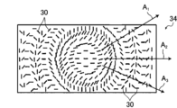
- FIG. 6 is a plan view conceptually showing another example of the optically anisotropic layer of the present invention.
- the optically anisotropic layer may have a liquid crystal alignment pattern radially arranged from the center.
- the direction of the optical axis (not shown) changes while continuously rotating along a number of directions from the center of the optically anisotropic layer 34 toward the outside, for example, the direction indicated by the arrow A1 , the direction indicated by the arrow A2 , the direction indicated by the arrow A3 , .... That is, the arrows A1 , A2 , and A3 are the alignment axes.
- the optical axes of the liquid crystal compound 30 change while rotating in the same direction from the center to the outside of the optically anisotropic layer 34.
- the rotation direction of the optical axes that change along the arrows A1 , A2 , and A3 in the figure becomes counterclockwise from the center to the outside.
- the lines connecting the liquid crystal compounds whose optical axes are oriented in the same direction form a circle, and the line segments of the circle form a concentric pattern.
- the optically anisotropic layer 34 having such a radial liquid crystal orientation pattern can focus transmitted light when the incident light is diffracted along each direction ( A1 to A3 , etc.) so that the azimuth direction is toward the center.
- the optically anisotropic layer 34 can diffuse transmitted light when the incident light is diffracted along each direction ( A1 to A3 ) so that the azimuth direction is toward the outside. Whether the transmitted light is diffracted toward the center or the outside depends on the polarization state of the incident light and the rotation direction of the optical axis in the liquid crystal orientation pattern.
- the liquid crystal alignment pattern of the optically anisotropic layer into such a radial pattern, it is possible to make it into a lens for converging or diverging light.
- the optical element is configured so that the diffraction angle gradually increases from the center to the outside, thereby allowing the optical element to more suitably focus or diverge light.
- FIG. 6 An optically anisotropic layer having a radial liquid crystal alignment pattern as shown in FIG. 6 can be formed, for example, by using an alignment film having an alignment pattern that aligns liquid crystal compounds in a radial liquid crystal alignment pattern.
- FIG. 7 conceptually shows another example of an exposure apparatus for forming an alignment pattern by exposing an alignment film.
- a light source 84 equipped with a laser 82, a polarizing beam splitter 86 that splits laser light M from the laser 82 into S-polarized light MS and P-polarized light MP, a mirror 90A arranged in the optical path of the P-polarized light MP and a mirror 90B arranged in the optical path of the S-polarized light MS, a lens 92 arranged in the optical path of the S-polarized light MS, a polarizing beam splitter 94, and a ⁇ /4 plate 96.
- the P-polarized light MP split by the polarizing beam splitter 86 is reflected by a mirror 90A and enters a polarizing beam splitter 94.
- the S-polarized light MS split by the polarizing beam splitter 86 is reflected by a mirror 90B, collected by a lens 92, and enters the polarizing beam splitter 94.
- the P-polarized light MP and the S-polarized light MS are combined by the polarizing beam splitter 94 and converted by the ⁇ /4 plate 96 into right-handed circularly polarized light and left-handed circularly polarized light according to the polarization direction, and enter the alignment film 18 on the support 12 .
- the polarization state of the light irradiated onto the alignment film 18 changes periodically in the form of interference fringes.
- the crossing angle between the left-handed and right-handed circularly polarized light changes from the inside to the outside of the concentric circles, an exposure pattern whose period changes from the inside to the outside is obtained.
- a radial alignment pattern in which the alignment state changes periodically is obtained in the alignment film 18.
- the length ⁇ of one period of the liquid crystal orientation pattern in which the optical axis of the liquid crystal compound 30 is continuously rotated by 180° can be controlled by changing the refractive power of the lens 92 (the F-number of the lens 92), the focal length of the lens 92, and the distance between the lens 92 and the orientation film 18, etc.
- the refractive power of the lens 92 the F-number of the lens 92
- the length ⁇ of one period of the liquid crystal orientation pattern can be changed in one direction in which the optical axis rotates continuously.
- the length ⁇ of one period of the liquid crystal orientation pattern can be changed in one direction in which the optical axis rotates continuously by the spread angle of the light spread by the lens 92 that interferes with the parallel light. More specifically, when the refractive power of the lens 92 is weakened, the light approaches parallel light, so that the length ⁇ of one period of the liquid crystal orientation pattern gradually shortens from the inside to the outside, and the F-number becomes larger. Conversely, when the refractive power of the lens 92 is strengthened, the length ⁇ of one period of the liquid crystal orientation pattern suddenly shortens from the inside to the outside, and the F-number becomes smaller.
- the optical element of the present invention comprises the above-mentioned optically anisotropic layer.
- An example of the configuration of the optical element is a laminate comprising a support, an alignment film, and the optically anisotropic layer of the present invention, which are integrally arranged in this order.
- the support, alignment film, and optically anisotropic layer are as described above.
- Other examples of the configuration of the optical element include a laminate having no support, an alignment film and the optically anisotropic layer of the present invention, a laminate having no alignment film, a support and the optically anisotropic layer of the present invention, and an embodiment having no support or alignment film and only the optically anisotropic layer of the present invention.
- the optical element may be an optical element that can be used as an optical element that transmits and refracts visible light.
- the optical element is not limited to the above-mentioned aspects, and may have a configuration that refracts and transmits infrared light and/or ultraviolet light, for example.
- the optical element of the present invention can be used in a variety of applications that transmit light in a direction different from the incident direction, such as a polarizing diffraction element in an optical device, an optical path changing component, a light focusing element, and an element for diffusing light in a specific direction.
- the image display device of the present invention is an image display device including the above-mentioned optical element.
- image display devices include augmented reality (AR) glasses, head-mounted displays such as virtual reality (VR), liquid crystal display devices, and projectors.
- AR augmented reality
- VR virtual reality
- LCD liquid crystal display devices
- the image display device when the image display device is AR glasses, it is sufficient that the image display device has the same configuration as known AR glasses except for having the optical elements described above, and may have, for example, a display element for projecting an image, a projection lens, a ⁇ /4 plate, a linear polarizing plate, etc.
- a projection lens a known projection lens (condenser lens) used in AR glasses or the like can be used.
- Examples of display elements include liquid crystal displays (including LCOS: Liquid Crystal On Silicon, etc.), organic electroluminescence displays, DLP (Digital Light Processing), and scanning displays using MEMS (Micro Electro Mechanical Systems) mirrors.
- the display element may be one that displays a monochrome image (single-color image), one that displays a two-color image, or one that displays a color image.
- the light emitted by the display element may be unpolarized or polarized, but is preferably circularly polarized.
- the image display device preferably further includes a circular polarizer consisting of a linear polarizer and a ⁇ /4 plate.
- the image display device preferably further includes, for example, a ⁇ /4 plate.
- the light emitted by the display element may be polarized light other than circularly polarized light, such as linearly polarized light.
- optically anisotropic layer, optical element, and image display device of the present invention have been described in detail above.
- the present invention is not limited to the above examples, and various improvements and modifications may be made without departing from the gist of the present invention.
- the following coating solution for forming an alignment film was applied onto the support by spin coating.
- the support on which the coating film of the coating solution for forming an alignment film was formed was dried on a hot plate at 60° C. for 60 seconds to form an alignment film.
- the alignment film was exposed using the exposure device shown in FIG. 5 to form an alignment film P-1 having an alignment pattern. More specifically, the support with the alignment film formed by the above method was placed in the exposure section of an exposure device, and the alignment film was exposed to interference light of two light beams MA and MB, thereby forming a pattern alignment film having an alignment pattern in which the alignment state changes periodically.
- the exposure device used was a laser emitting laser light with a wavelength of 355 nm.
- the exposure amount of the alignment film to the interference light was 1000 mJ/ cm2 .
- composition A-1 As a liquid crystal composition for forming an optically anisotropic layer, the following composition A-1 was prepared.
- Composition A-1 ⁇ Liquid crystal compound L-1 80.00 parts by mass Liquid crystal compound L-2 20.00 parts by mass Polymerization initiator P-1 3.00 parts by mass Leveling agent T-1 0.40 parts by mass Methyl ethyl ketone 522.00 parts by mass Cyclopentanone 522.00 parts by mass
- An optically anisotropic layer was formed by applying composition A-1 in multiple layers onto alignment film P-1.
- Multi-layer application refers to first applying composition A-1 as the first layer onto the alignment film, heating it and curing it with UV light to create a liquid crystal fixing layer, and then applying layers from the second layer onwards to the liquid crystal fixing layer, and similarly heating it and curing it with UV light, and repeating this process.
- the following composition A-1 was applied onto the alignment film P-1, and the coating film was heated to 80°C on a hot plate. Thereafter, the coating film was irradiated with ultraviolet light having a wavelength of 365 nm using a high-pressure mercury lamp under a nitrogen atmosphere at an illuminance of 10 mW/ cm2 and an exposure dose of 200 mJ/cm2, thereby fixing the alignment of the liquid crystal compound.
- the length ⁇ of one period in which the optical axis derived from the liquid crystal compound rotates 180° along the X direction, in which the direction of the optical axis derived from the liquid crystal compound changes while rotating continuously was 4.0 ⁇ m over the entire surface of the liquid crystal orientation pattern of the optically anisotropic layer of the liquid crystal diffraction element 1.
- Examples 2 to 6, 11 to 12 Except for using compositions A-2 to A-8 having the compositions shown in Table 1 below instead of composition A-1 as the liquid crystal composition for forming the optically anisotropic layer, the optically anisotropic layer was formed in the same manner as in Example 1, and liquid crystal diffraction elements 2 to 6 and 11 to 12 each having a support, an alignment film, and an optically anisotropic layer were prepared.
- the crossing angle ⁇ of the two light beams MA and MB irradiated onto the alignment film before the alignment pattern is formed is adjusted to form alignment films P-2 to P-4 having different alignment patterns with different lengths ⁇ of one period in which the optical axis rotates 180° in the X direction in which the direction of the optical axis derived from the liquid crystal compound changes while rotating.
- an optically anisotropic layer was formed in the same manner as in Example 6, and liquid crystal diffraction elements 7 to 9 each having a support, an alignment film, and an optically anisotropic layer were produced.
- Example 10 In forming an optically anisotropic layer, the composition A-6 was used to form an optically anisotropic layer on the alignment film P-4 or on the liquid crystal fixation layer formed immediately before, and then the coating film was heated, and ultraviolet light having a wavelength of 365 nm was irradiated under the conditions of an illuminance of 200 mW/ cm2 and an exposure dose of 200 mJ/ cm2 . Except for this, an optically anisotropic layer was formed in the same manner as in Example 9, and a liquid crystal diffraction element 10 having a support, an alignment film, and an optically anisotropic layer was produced.
- Example 1 A liquid crystal diffraction element C1 having a support, an alignment film and an optically anisotropic layer was prepared in the same manner as in Example 1, except that a composition A-9 having a composition shown in Table 1 below was used instead of composition A-1 as the liquid crystal composition for forming the optically anisotropic layer, and that a coating film formed on the alignment film P-1 or on the liquid crystal fixing layer formed immediately before using composition A-1 and then heated was irradiated with ultraviolet light having a wavelength of 365 nm at an illuminance of 200 mW/cm 2 and an exposure dose of 200 mJ/cm 2 when the optically anisotropic layer was formed.
- a composition A-9 having a composition shown in Table 1 below was used instead of composition A-1 as the liquid crystal composition for forming the optically anisotropic layer
- a coating film formed on the alignment film P-1 or on the liquid crystal fixing layer formed immediately before using composition A-1 and then heated was irradiated with ultraviolet light having a wavelength of 365
- Table 1 shows the formulations of the liquid crystal compositions used to form the optically anisotropic layers used in each Example and Comparative Example 1.
- Additive A-1 Karenz MT (registered trademark) BD1 (1,4-bis(3-mercaptobutyryloxy)butane) manufactured by Showa Denko K.K.
- Additive A-2 "Sumilizer (registered trademark) GM” manufactured by Sumitomo Chemical Co., Ltd.
- a roughness curve representing the surface shape of the target section and an average line of the roughness curve were created, and the difference between the highest point and the lowest point on the roughness curve was calculated.
- the above measurements and calculations were performed on 10 randomly selected points on the surface of the formed optically anisotropic layer, and the arithmetic average value of the remaining 8 points excluding the highest and lowest values was determined as the maximum height d of the uneven structure formed on the surface of the optically anisotropic layer.
- the unit of the maximum height d of the uneven structure is "nm".
- Measurement mode WAVE mode Objective lens: 50x Measurement area: 124 ⁇ m x 93 ⁇ m
- ⁇ Average length P of one period of uneven structure> Based on the roughness curve representing the surface shape of the optically anisotropic layer, which was created by the above-mentioned method using the VertScan, the distance between the positions showing the maximum values of two adjacent convex portions in the X direction was calculated. The above calculation was performed for 10 points arbitrarily selected on the surface of the optically anisotropic layer, and the arithmetic average value of 8 points excluding the highest and lowest values was taken as the average length P of one period of the uneven structure formed on the surface of the optically anisotropic layer. The unit of the average length P of one period of the uneven structure is " ⁇ m".
- the length ⁇ of one period in which the optical axis derived from the liquid crystal compound rotates 180° in the X direction in which the optical axis derived from the liquid crystal compound changes while rotating continuously was equal to the average length P of one period of the uneven structure formed on the surface of the optically anisotropic layer.
- a right-handed circularly polarized light having a wavelength of 532 nm and an ellipticity ⁇ in of 0.95 or more (0.99) was incident toward the center of the liquid crystal diffraction element from the front side of the liquid crystal diffraction element (the direction of the angle 0° with respect to the normal line).
- the light intensity of the incident light incident on the liquid crystal diffraction element and the light intensity of the zeroth-order light among the outgoing light transmitted through the liquid crystal diffraction element and emitted from the circular polarizer were measured by a photodetector, and the light amount of the zeroth-order light (the light amount of the zeroth-order light when the light amount of the incident light is set to 1) was calculated by the following formula.
- Amount of 0th order light (%) Light intensity of 0th order light / Light intensity of incident light ⁇ 100
- the zero-order light suppression performance was evaluated based on the calculated amount of zero-order light and the following evaluation criteria. The lower the amount of zero-order light, the more the transmission of zero-order light through the optically anisotropic layer is suppressed, and the more the stray light transmitted through the circular polarizer can be suppressed.
- Table 2 shows the numbers of the compositions used to form the optically anisotropic layers, the curing conditions when the optically anisotropic layers were formed, the physical properties of the formed optically anisotropic layers, and the above evaluation results.
- the " ⁇ ( ⁇ m)" column indicates the length ⁇ (unit: ⁇ m) of one period in the liquid crystal alignment pattern of each optically anisotropic layer, measured using a polarizing microscope.
- the length ⁇ of one period was the value shown in the " ⁇ ( ⁇ m)" column in the table over the entire surface of the liquid crystal alignment pattern of the formed optically anisotropic layer.
- the "P ( ⁇ m)” column indicates the measured value (unit: ⁇ m) of the average length P of one period of the unevenness structure measured by the above method
- the "d ( ⁇ m)” column indicates the measured value (unit: nm) of the maximum height d of the unevenness structure measured by the above method.
- the " ⁇ ” column indicates the value ⁇ calculated using the above formula (1) from the length of one period ⁇ ( ⁇ m) and the maximum height d (nm) of the concave-convex structure.
Landscapes
- Physics & Mathematics (AREA)
- General Physics & Mathematics (AREA)
- Optics & Photonics (AREA)
- Engineering & Computer Science (AREA)
- Theoretical Computer Science (AREA)
- Polarising Elements (AREA)
Priority Applications (1)
| Application Number | Priority Date | Filing Date | Title |
|---|---|---|---|
| JP2025543416A JPWO2025047594A1 (cg-RX-API-DMAC7.html) | 2023-08-25 | 2024-08-23 |
Applications Claiming Priority (2)
| Application Number | Priority Date | Filing Date | Title |
|---|---|---|---|
| JP2023-137250 | 2023-08-25 | ||
| JP2023137250 | 2023-08-25 |
Publications (1)
| Publication Number | Publication Date |
|---|---|
| WO2025047594A1 true WO2025047594A1 (ja) | 2025-03-06 |
Family
ID=94819164
Family Applications (1)
| Application Number | Title | Priority Date | Filing Date |
|---|---|---|---|
| PCT/JP2024/029937 Ceased WO2025047594A1 (ja) | 2023-08-25 | 2024-08-23 | 光学異方性層、光学素子、画像表示装置 |
Country Status (2)
| Country | Link |
|---|---|
| JP (1) | JPWO2025047594A1 (cg-RX-API-DMAC7.html) |
| WO (1) | WO2025047594A1 (cg-RX-API-DMAC7.html) |
Citations (7)
| Publication number | Priority date | Publication date | Assignee | Title |
|---|---|---|---|---|
| WO2022050321A1 (ja) * | 2020-09-02 | 2022-03-10 | 富士フイルム株式会社 | 液晶回折素子、光学素子、画像表示ユニット、ヘッドマウントディスプレイ、ビームステアリングおよびセンサー |
| WO2022050319A1 (ja) * | 2020-09-02 | 2022-03-10 | 富士フイルム株式会社 | 液晶回折素子、光学素子、画像表示ユニット、ヘッドマウントディスプレイ、ビームステアリング、および、センサー |
| WO2022270564A1 (ja) * | 2021-06-23 | 2022-12-29 | 富士フイルム株式会社 | 化合物、組成物、硬化物、光学異方体、光学素子及び導光素子 |
| WO2022270563A1 (ja) * | 2021-06-23 | 2022-12-29 | 富士フイルム株式会社 | 化合物、組成物、硬化物、光学異方体、光学素子、及び導光素子 |
| JP2023003351A (ja) * | 2021-06-23 | 2023-01-11 | 富士フイルム株式会社 | 化合物、組成物、硬化物、光学異方体、光学素子及び導光素子 |
| WO2023127538A1 (ja) * | 2021-12-28 | 2023-07-06 | 富士フイルム株式会社 | 液晶性組成物、硬化物、光学異方性層、光学素子、導光素子 |
| WO2024143339A1 (ja) * | 2022-12-28 | 2024-07-04 | 富士フイルム株式会社 | 光学異方性層、導光素子およびar表示デバイス |
-
2024
- 2024-08-23 JP JP2025543416A patent/JPWO2025047594A1/ja active Pending
- 2024-08-23 WO PCT/JP2024/029937 patent/WO2025047594A1/ja not_active Ceased
Patent Citations (7)
| Publication number | Priority date | Publication date | Assignee | Title |
|---|---|---|---|---|
| WO2022050321A1 (ja) * | 2020-09-02 | 2022-03-10 | 富士フイルム株式会社 | 液晶回折素子、光学素子、画像表示ユニット、ヘッドマウントディスプレイ、ビームステアリングおよびセンサー |
| WO2022050319A1 (ja) * | 2020-09-02 | 2022-03-10 | 富士フイルム株式会社 | 液晶回折素子、光学素子、画像表示ユニット、ヘッドマウントディスプレイ、ビームステアリング、および、センサー |
| WO2022270564A1 (ja) * | 2021-06-23 | 2022-12-29 | 富士フイルム株式会社 | 化合物、組成物、硬化物、光学異方体、光学素子及び導光素子 |
| WO2022270563A1 (ja) * | 2021-06-23 | 2022-12-29 | 富士フイルム株式会社 | 化合物、組成物、硬化物、光学異方体、光学素子、及び導光素子 |
| JP2023003351A (ja) * | 2021-06-23 | 2023-01-11 | 富士フイルム株式会社 | 化合物、組成物、硬化物、光学異方体、光学素子及び導光素子 |
| WO2023127538A1 (ja) * | 2021-12-28 | 2023-07-06 | 富士フイルム株式会社 | 液晶性組成物、硬化物、光学異方性層、光学素子、導光素子 |
| WO2024143339A1 (ja) * | 2022-12-28 | 2024-07-04 | 富士フイルム株式会社 | 光学異方性層、導光素子およびar表示デバイス |
Also Published As
| Publication number | Publication date |
|---|---|
| JPWO2025047594A1 (cg-RX-API-DMAC7.html) | 2025-03-06 |
Similar Documents
| Publication | Publication Date | Title |
|---|---|---|
| CN115605785B (zh) | 透射型液晶衍射元件 | |
| JP7515601B2 (ja) | 液晶回折素子、光学素子、画像表示ユニット、ヘッドマウントディスプレイ、ビームステアリング、および、センサー | |
| CN113168016A (zh) | 导光元件、图像显示装置及传感装置 | |
| JP7561763B2 (ja) | 画像表示装置 | |
| JP7431986B2 (ja) | 画像表示ユニットおよびヘッドマウントディスプレイ | |
| JP7483111B2 (ja) | 光学素子および画像表示装置 | |
| US12181771B2 (en) | Transmissive liquid crystal diffraction element | |
| US11886071B2 (en) | Light guide element comprising a diffraction element having a cholesteric liquid crystal layer with a pitch gradient | |
| JPWO2020075702A1 (ja) | 光学素子および画像表示装置 | |
| JP2021107871A (ja) | 投映型画像表示システム | |
| WO2023189884A1 (ja) | 液晶回折素子、光学素子、画像表示ユニット、ヘッドマウントディスプレイ、ビームステアリングおよびセンサー | |
| WO2023101014A1 (ja) | ビームコンバイナ、配向膜の形成方法、および、光学素子の製造方法 | |
| WO2022264908A1 (ja) | 透過型液晶回折素子 | |
| JP7360481B2 (ja) | 光学素子および画像表示装置 | |
| WO2022239835A1 (ja) | 光学素子、画像表示装置、ヘッドマウントディスプレイ、センシング装置、アイトラッキング装置 | |
| US20240027783A1 (en) | Beam combiner, method of forming alignment film, and method of manufacturing optical element | |
| JP7433434B2 (ja) | 光学異方性膜、光学素子、光学システム | |
| CN118176448A (zh) | 光学元件及图像显示装置 | |
| WO2024204065A1 (ja) | 光学積層体、表示装置、センサー | |
| WO2024070693A1 (ja) | 偏光回折素子、光学素子および光学装置 | |
| WO2022239859A1 (ja) | 光学素子、画像表示装置、ヘッドマウントディスプレイ、センシング装置、アイトラッキング装置 | |
| WO2021131709A1 (ja) | 投映型画像表示システム | |
| JP7545296B2 (ja) | 画像表示システム | |
| CN118742831A (zh) | 衍射元件 | |
| WO2025126979A1 (ja) | 光学素子 |
Legal Events
| Date | Code | Title | Description |
|---|---|---|---|
| 121 | Ep: the epo has been informed by wipo that ep was designated in this application |
Ref document number: 24859627 Country of ref document: EP Kind code of ref document: A1 |
|
| ENP | Entry into the national phase |
Ref document number: 2025543416 Country of ref document: JP Kind code of ref document: A |
|
| WWE | Wipo information: entry into national phase |
Ref document number: 2025543416 Country of ref document: JP |
|
| NENP | Non-entry into the national phase |
Ref country code: DE |