WO2025046720A1 - 半導体製造装置用部材 - Google Patents
半導体製造装置用部材 Download PDFInfo
- Publication number
- WO2025046720A1 WO2025046720A1 PCT/JP2023/031085 JP2023031085W WO2025046720A1 WO 2025046720 A1 WO2025046720 A1 WO 2025046720A1 JP 2023031085 W JP2023031085 W JP 2023031085W WO 2025046720 A1 WO2025046720 A1 WO 2025046720A1
- Authority
- WO
- WIPO (PCT)
- Prior art keywords
- central
- ceramic member
- outer peripheral
- semiconductor manufacturing
- manufacturing equipment
- Prior art date
- Legal status (The legal status is an assumption and is not a legal conclusion. Google has not performed a legal analysis and makes no representation as to the accuracy of the status listed.)
- Pending
Links
Images






Classifications
-
- H—ELECTRICITY
- H01—ELECTRIC ELEMENTS
- H01J—ELECTRIC DISCHARGE TUBES OR DISCHARGE LAMPS
- H01J37/00—Discharge tubes with provision for introducing objects or material to be exposed to the discharge, e.g. for the purpose of examination or processing thereof
- H01J37/32—Gas-filled discharge tubes
- H01J37/32431—Constructional details of the reactor
- H01J37/32623—Mechanical discharge control means
- H01J37/32642—Focus rings
-
- H—ELECTRICITY
- H10—SEMICONDUCTOR DEVICES; ELECTRIC SOLID-STATE DEVICES NOT OTHERWISE PROVIDED FOR
- H10P—GENERIC PROCESSES OR APPARATUS FOR THE MANUFACTURE OR TREATMENT OF DEVICES COVERED BY CLASS H10
- H10P72/00—Handling or holding of wafers, substrates or devices during manufacture or treatment thereof
- H10P72/04—Apparatus for manufacture or treatment
- H10P72/0431—Apparatus for thermal treatment
- H10P72/0432—Apparatus for thermal treatment mainly by conduction
-
- H—ELECTRICITY
- H10—SEMICONDUCTOR DEVICES; ELECTRIC SOLID-STATE DEVICES NOT OTHERWISE PROVIDED FOR
- H10P—GENERIC PROCESSES OR APPARATUS FOR THE MANUFACTURE OR TREATMENT OF DEVICES COVERED BY CLASS H10
- H10P72/00—Handling or holding of wafers, substrates or devices during manufacture or treatment thereof
- H10P72/70—Handling or holding of wafers, substrates or devices during manufacture or treatment thereof for supporting or gripping
- H10P72/72—Handling or holding of wafers, substrates or devices during manufacture or treatment thereof for supporting or gripping using electrostatic chucks
-
- H—ELECTRICITY
- H10—SEMICONDUCTOR DEVICES; ELECTRIC SOLID-STATE DEVICES NOT OTHERWISE PROVIDED FOR
- H10P—GENERIC PROCESSES OR APPARATUS FOR THE MANUFACTURE OR TREATMENT OF DEVICES COVERED BY CLASS H10
- H10P72/00—Handling or holding of wafers, substrates or devices during manufacture or treatment thereof
- H10P72/70—Handling or holding of wafers, substrates or devices during manufacture or treatment thereof for supporting or gripping
- H10P72/72—Handling or holding of wafers, substrates or devices during manufacture or treatment thereof for supporting or gripping using electrostatic chucks
- H10P72/722—Details of electrostatic chucks
-
- H—ELECTRICITY
- H10—SEMICONDUCTOR DEVICES; ELECTRIC SOLID-STATE DEVICES NOT OTHERWISE PROVIDED FOR
- H10P—GENERIC PROCESSES OR APPARATUS FOR THE MANUFACTURE OR TREATMENT OF DEVICES COVERED BY CLASS H10
- H10P72/00—Handling or holding of wafers, substrates or devices during manufacture or treatment thereof
- H10P72/70—Handling or holding of wafers, substrates or devices during manufacture or treatment thereof for supporting or gripping
- H10P72/76—Handling or holding of wafers, substrates or devices during manufacture or treatment thereof for supporting or gripping using mechanical means, e.g. clamps or pinches
- H10P72/7604—Handling or holding of wafers, substrates or devices during manufacture or treatment thereof for supporting or gripping using mechanical means, e.g. clamps or pinches the wafers being placed on a susceptor, stage or support
- H10P72/7611—Handling or holding of wafers, substrates or devices during manufacture or treatment thereof for supporting or gripping using mechanical means, e.g. clamps or pinches the wafers being placed on a susceptor, stage or support characterised by edge profile or support profile
-
- H—ELECTRICITY
- H10—SEMICONDUCTOR DEVICES; ELECTRIC SOLID-STATE DEVICES NOT OTHERWISE PROVIDED FOR
- H10P—GENERIC PROCESSES OR APPARATUS FOR THE MANUFACTURE OR TREATMENT OF DEVICES COVERED BY CLASS H10
- H10P72/00—Handling or holding of wafers, substrates or devices during manufacture or treatment thereof
- H10P72/70—Handling or holding of wafers, substrates or devices during manufacture or treatment thereof for supporting or gripping
- H10P72/76—Handling or holding of wafers, substrates or devices during manufacture or treatment thereof for supporting or gripping using mechanical means, e.g. clamps or pinches
- H10P72/7604—Handling or holding of wafers, substrates or devices during manufacture or treatment thereof for supporting or gripping using mechanical means, e.g. clamps or pinches the wafers being placed on a susceptor, stage or support
- H10P72/7616—Handling or holding of wafers, substrates or devices during manufacture or treatment thereof for supporting or gripping using mechanical means, e.g. clamps or pinches the wafers being placed on a susceptor, stage or support characterised by a coating, a hardness or a material
-
- H—ELECTRICITY
- H10—SEMICONDUCTOR DEVICES; ELECTRIC SOLID-STATE DEVICES NOT OTHERWISE PROVIDED FOR
- H10P—GENERIC PROCESSES OR APPARATUS FOR THE MANUFACTURE OR TREATMENT OF DEVICES COVERED BY CLASS H10
- H10P72/00—Handling or holding of wafers, substrates or devices during manufacture or treatment thereof
- H10P72/70—Handling or holding of wafers, substrates or devices during manufacture or treatment thereof for supporting or gripping
- H10P72/76—Handling or holding of wafers, substrates or devices during manufacture or treatment thereof for supporting or gripping using mechanical means, e.g. clamps or pinches
- H10P72/7604—Handling or holding of wafers, substrates or devices during manufacture or treatment thereof for supporting or gripping using mechanical means, e.g. clamps or pinches the wafers being placed on a susceptor, stage or support
- H10P72/7624—Handling or holding of wafers, substrates or devices during manufacture or treatment thereof for supporting or gripping using mechanical means, e.g. clamps or pinches the wafers being placed on a susceptor, stage or support characterised by the mechanical construction of the susceptor, stage or support
-
- H—ELECTRICITY
- H01—ELECTRIC ELEMENTS
- H01J—ELECTRIC DISCHARGE TUBES OR DISCHARGE LAMPS
- H01J2237/00—Discharge tubes exposing object to beam, e.g. for analysis treatment, etching, imaging
- H01J2237/32—Processing objects by plasma generation
- H01J2237/33—Processing objects by plasma generation characterised by the type of processing
- H01J2237/332—Coating
- H01J2237/3322—Problems associated with coating
- H01J2237/3323—Problems associated with coating uniformity
-
- H—ELECTRICITY
- H01—ELECTRIC ELEMENTS
- H01J—ELECTRIC DISCHARGE TUBES OR DISCHARGE LAMPS
- H01J2237/00—Discharge tubes exposing object to beam, e.g. for analysis treatment, etching, imaging
- H01J2237/32—Processing objects by plasma generation
- H01J2237/33—Processing objects by plasma generation characterised by the type of processing
- H01J2237/334—Etching
- H01J2237/3343—Problems associated with etching
Definitions
- the present invention relates to components for semiconductor manufacturing equipment.
- the holding device of Patent Document 1 has a central electrostatic chuck section that mainly holds the wafer and an outer periphery electrostatic chuck section that mainly holds the focus ring.
- the central electrostatic chuck section includes a central ceramic member to which the wafer is attracted on the upper surface, and a metal central base member joined to the lower surface of the central ceramic member by a resin central joint.
- the outer periphery electrostatic chuck section includes a peripheral ceramic member to which the focus ring is attracted on the upper surface, and a metal central base member joined to the lower surface of the peripheral ceramic member by a resin peripheral joint.
- the outer periphery electrostatic chuck section is a substantially annular member that surrounds the central electrostatic chuck section in a plan view.
- the outer periphery electrostatic chuck section is a separate body from the central electrostatic chuck section, and there is a gap between the central electrostatic chuck section and the central electrostatic chuck section.
- the present invention was made to solve these problems, and its main objective is to prevent the deterioration of the device's lifespan.
- the semiconductor manufacturing equipment member of the present invention comprises: a central ceramic member having a wafer mounting surface thereon; an annular peripheral ceramic member having a focus ring mounting surface on an upper surface thereof and disposed on an outer circumferential side of the central ceramic member; a central support part joined to a lower surface of the central ceramic member and supporting the central ceramic member, and a peripheral support part joined to a lower surface of the peripheral ceramic member and supporting the peripheral ceramic member, the central support part and the peripheral support part being separate or integral with each other;
- the diameter of the outer peripheral surface of the central ceramic member and the inner peripheral surface of the outer peripheral ceramic member both change in the up-down direction,
- the maximum diameter of the outer circumferential surface of the central ceramic member is smaller than the maximum diameter of the inner circumferential surface of the outer circumferential ceramic member and is larger than the minimum diameter of the inner circumferential surface of the outer circumferential ceramic member.
- the diameters of the outer peripheral surface of the central ceramic member and the inner peripheral surface of the outer peripheral ceramic member both change in the vertical direction.
- the maximum diameter of the outer peripheral surface of the central ceramic member is smaller than the maximum diameter of the inner peripheral surface of the outer peripheral ceramic member and is smaller than the minimum diameter of the inner peripheral surface of the outer peripheral ceramic member. Therefore, when the semiconductor manufacturing equipment component is viewed in a plan view, the outer peripheral portion of the central ceramic member and the inner peripheral portion of the outer peripheral ceramic member overlap.
- ions accelerated toward the semiconductor manufacturing equipment component during plasma processing collide with the ceramic member before reaching the base member or the joint, and do not proceed beyond that. This suppresses the generation of plasma and radicals around the base member and the joint, and as a result, the deterioration of the equipment life can be suppressed.
- the minimum diameter of the outer peripheral surface of the central ceramic component may be smaller than the minimum diameter of the inner peripheral surface of the outer peripheral ceramic component.
- Such a central ceramic component and an outer peripheral ceramic component can be produced, for example, by hollowing out a single ceramic plate.
- the outer peripheral surface of the central ceramic member and the inner peripheral surface of the peripheral ceramic member may each appear as a diagonal line in a cross section of the semiconductor manufacturing equipment component cut in a direction perpendicular to the wafer mounting surface.
- Such a central ceramic member and peripheral ceramic member may be produced, for example, by hollowing out a single ceramic plate into a truncated cone shape or an inverted truncated cone shape.
- the outer peripheral surface of the central ceramic component may be a tapered surface whose diameter increases toward the top.
- the outer peripheral surface of the central ceramic component may be a tapered surface whose diameter decreases toward the top.
- the outer peripheral support part may be an annular part arranged on the outer periphery of the central support part with a gap therebetween. This makes it easier to control the temperature of the outer peripheral support part and the temperature of the central support part separately, which in turn makes it easier to control the temperature of the wafer mounting surface and the temperature of the focus ring mounting surface separately.
- the central ceramic member and the central support part may be joined by a metallic central joint part, the outer peripheral surface of the central joint part together with the outer peripheral surface of the central support part being covered by a central insulating film, and the outer peripheral ceramic member and the outer peripheral support part may be joined by a metallic outer peripheral joint part, the inner peripheral surface of the outer peripheral joint part together with the inner peripheral surface of the outer peripheral support part being covered by an outer peripheral insulating film.
- the joint part and the base member are covered by an insulating film, corrosion of the joint part and the base member is further suppressed.
- the joint part is made of metal and not resin, the joint part is less likely to deteriorate even if an insulating film is formed by thermal spraying or the like.
- the central ceramic member and the central support part may be joined by a central joint part made of resin, and the peripheral ceramic member and the peripheral support part may be joined by a peripheral joint part made of resin. Since the resin adhesive layer is easily corroded, it is highly meaningful to apply the present invention.
- the semiconductor manufacturing equipment member of the present invention may comprise an annular peripheral ceramic member having a focus ring mounting surface on its upper surface and configured to be arranged on the outer periphery of a central ceramic member having a wafer mounting surface, and a conductive base member joined to the lower surface of the peripheral ceramic member and having an outer periphery support portion that supports the peripheral ceramic member, the inner peripheral surface of the peripheral ceramic member having a diameter that changes in the vertical direction, and the inner peripheral surface of the peripheral ceramic member is a tapered surface in which the diameter increases toward the upper side or decreases toward the upper side, for mounting a focus ring.
- FIG. 2 is a longitudinal sectional view of a semiconductor manufacturing equipment member 10.
- FIG. 2 is a plan view of a semiconductor manufacturing equipment member 10.
- FIG. 2 is a partially enlarged view of FIG. 3 is a manufacturing process diagram of the central ceramic member 22 and the peripheral ceramic member 32.
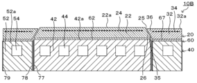
- FIG. 10 is a vertical cross-sectional view of a semiconductor manufacturing equipment member 10B according to another embodiment of the present invention.
- FIG. 10 is a plan view of a semiconductor manufacturing equipment member 10B according to another embodiment of the present invention.
- FIG. 6 is a partially enlarged view of FIG. 5 .
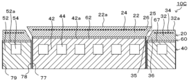
- FIG. 10 is a longitudinal sectional view of a semiconductor manufacturing equipment member 10C according to another embodiment of the present invention.
- FIG. 10 is a vertical cross-sectional view of a semiconductor manufacturing equipment member 10D according to another embodiment of the present invention.
- FIG. 4 is a partial enlarged view of a semiconductor manufacturing equipment member 110 according to a comparative example.
- FIG. 1 is a vertical cross-sectional view of a semiconductor manufacturing equipment member 10 (a cross-sectional view taken along a plane including the central axis of the semiconductor manufacturing equipment member 10).
- FIG. 2 is a plan view of the semiconductor manufacturing equipment member 10.
- FIG. 3 is a partially enlarged view of FIG. 1.
- FIG. 4 is a manufacturing process diagram of the central ceramic member 22 and the peripheral ceramic member 32.
- the semiconductor manufacturing equipment member 10 is used to perform CVD, etching, etc. on a wafer W using plasma, and is fixed to a mounting plate 84 provided inside a semiconductor process chamber 80.
- the semiconductor manufacturing equipment member 10 includes a central ceramic member 22, a peripheral ceramic member 32, and a base member 40.
- the base member 40 includes a central base member 42 as a central support portion and a peripheral base member 52 as a peripheral support portion.
- the central ceramic member 22 and the central base member 42 are joined at a central joint 62.
- the peripheral ceramic member 32 and the peripheral base member 52 are joined at a peripheral joint 67.
- the central ceramic member 22 and the peripheral ceramic member 32 are collectively referred to as ceramic member 20.
- the central joint 62 and the peripheral joint 67 are collectively referred to as joint 60.
- the semiconductor manufacturing equipment member 10 may include a focus ring 70.
- focus ring is abbreviated as "FR”.
- the central ceramic member 22 is a ceramic disk member having a circular wafer mounting surface 22a on the upper surface.
- the wafer W is mounted on the wafer mounting surface 22a.
- the diameter of the wafer mounting surface 22a is smaller than the diameter of the wafer W (e.g., 300 mm).
- the central ceramic member 22 is formed of a ceramic material such as alumina or aluminum nitride.
- the central ceramic member 22 has a wafer adsorption electrode 24 built in.
- the wafer adsorption electrode 24 is formed of a material containing, for example, W, Mo, WC, MoC, etc.
- the wafer adsorption electrode 24 is a plate-shaped or mesh-shaped monopolar electrostatic electrode.
- the layer of the central ceramic member 22 above the wafer adsorption electrode 24 functions as a dielectric layer.
- the wafer adsorption electrode 24 is connected to a DC power source for wafer adsorption (not shown).
- the outer ceramic member 32 is an annular member and has an annular FR mounting surface 32a on the upper surface.
- the outer ceramic member 32 is separate from the central ceramic member 22 and is disposed on the outer periphery of the central ceramic member 22 with a gap therebetween.
- the FR mounting surface 32a is provided at a position one step lower than the wafer mounting surface 22a.
- the FR 70 is mounted on the FR mounting surface 32a.
- the inner diameter of the FR mounting surface 32a is approximately the same as the inner diameter of the FR 70.
- the outer ceramic member 32 is formed of a ceramic material such as alumina or aluminum nitride.
- the outer ceramic member 32 has an FR adsorption electrode 34 built in.
- the FR adsorption electrode 34 is formed of a material containing, for example, W, Mo, WC, MoC, etc.
- the FR adsorption electrode 34 is a plate-shaped or mesh-shaped monopolar electrostatic electrode.
- the layer of the outer ceramic member 32 above the FR adsorption electrode 34 functions as a dielectric layer.
- the FR adsorption electrode 34 is connected to an FR adsorption DC power supply (not shown).
- the outer ceramic member 32 may have the same thickness as the central ceramic member 22.
- the outer peripheral surface 25 of the central ceramic member 22 is a tapered surface (the outer surface of an inverted truncated cone) whose diameter increases toward the top. As shown in FIG. 3, the outer peripheral surface 25 of the central ceramic member 22 is inclined toward the outer peripheral side by an angle ⁇ in the vertical direction starting from its lower end 25b. The angle ⁇ is, for example, 10° or more and 80° or less.
- the inner peripheral surface 35 of the outer peripheral ceramic member 32 is a tapered surface (the inner surface of an inverted truncated cone carved out of a disk) whose diameter increases toward the upper side. As shown in FIG. 3, the inner peripheral surface 35 of the outer peripheral ceramic member 32 is inclined toward the outer peripheral side by an angle ⁇ in the vertical direction starting from its lower end 35b.
- the angle ⁇ is, for example, 10° or more and 80° or less.
- the angle ⁇ may be the same as the angle ⁇ or may be different.
- the maximum diameter Pmax of the outer peripheral surface 25 of the central ceramic member 22 (the diameter of the upper end 25a of the outer peripheral surface 25 in this embodiment) is smaller than the maximum diameter Qmax of the inner peripheral surface 35 of the outer peripheral ceramic member 32 (the diameter of the upper end 35a of the inner peripheral surface 35 in this embodiment) and is larger than the minimum diameter Qmin of the inner peripheral surface 35 of the outer peripheral ceramic member 32 (the diameter of the lower end 35b of the inner peripheral surface 35 in this embodiment).
- the outer peripheral portion 26 of the central ceramic member 22 and the inner peripheral portion 36 of the outer peripheral ceramic member 32 overlap. Note that when the semiconductor manufacturing equipment member 10 is viewed in a plan view, the inner peripheral surface 35 of the outer peripheral ceramic member 32 is between the wafer mounting surface 22a and the FR mounting surface 32a, and it is not possible to see through it.
- FIG. 4 is a manufacturing process diagram of the central ceramic member 22 and the peripheral ceramic member 32.
- a ceramic plate 21 is prepared in which the wafer adsorption electrode 24 and the FR adsorption electrode 34 are embedded.
- This ceramic plate 21 is manufactured, for example, as follows. First, two circular molded bodies of ceramic powder are manufactured. Next, a central printed electrode having the same shape as the wafer adsorption electrode 24 and a peripheral printed electrode having the same shape as the FR adsorption electrode 34 are printed on the upper surface of the first circular molded body so as to be concentric with the circular molded body.
- a second circular molded body is laminated on the printed electrode surface of the first circular molded body to form a laminate.
- This laminate is hot-pressed and sintered to obtain the ceramic plate 21.
- the ceramic plate 21 is machined to cut out the disk-shaped central portion and separate it into an annular outer peripheral portion, thereby obtaining the central ceramic member 22 and the outer peripheral ceramic member 32.
- the disk-shaped central portion is machined to have an inverted truncated cone shape.
- the central ceramic member 22 and the outer peripheral ceramic member 32 are produced from one ceramic plate, it is easier to reduce manufacturing costs than when a ceramic plate for the central ceramic member 22 and a ceramic plate for the outer peripheral ceramic member 32 are separately prepared.
- the size of the gap between the central ceramic member 22 and the outer peripheral ceramic member 32 produced in this way can be adjusted simply by shifting their relative vertical positions, as shown in FIG. 4C.
- the outer peripheral surface 25 of the obtained central ceramic member 22 and the inner peripheral surface 35 of the outer peripheral ceramic member 32 may be further machined to provide irregularities.
- the central base member 42 is a conductive disk member and has a circular central support surface 42a on the upper surface.
- the central ceramic member 22 is joined to the central support surface 42a.
- the diameter of the central support surface 42a is the same as the diameter of the lower surface of the central ceramic member 22.
- the central base member 42 has a central refrigerant flow path 44 through which a refrigerant can circulate inside. This central refrigerant flow path 44 is provided in a single stroke across the entire central base member 42 in a plan view.
- the refrigerant flowing through the central refrigerant flow path 44 is preferably a liquid and is preferably electrically insulating. Examples of electrically insulating liquids include fluorine-based inert liquids.
- the central base member 42 is made of a conductive material containing, for example, a metal.
- conductive materials include metals and composite materials.
- metals include Al, Ti, Mo, and alloys thereof.
- composite materials include metal matrix composite materials (metal matrix composites (MMC)) and ceramic matrix composite materials (ceramic matrix composites (CMC)). Specific examples of such composite materials include materials containing Si, SiC, and Ti, and materials in which a porous SiC body is impregnated with Al and/or Si.
- a material containing Si, SiC, and Ti is called SiSiCTi
- a material in which a porous SiC body is impregnated with Al is called AlSiC
- a material in which a porous SiC body is impregnated with Si is called SiSiC.
- a material having a high thermal conductivity for the central base member 42 and for example, Al or an Al alloy is preferable.
- the central base member 42 is also used as an RF electrode.
- a central insulating film 77 made of an insulating material (for example, alumina or yttria) is formed on the outer circumferential surface of the central base member 42.
- the central insulating film 77 may be a thermal spray film.
- This outer peripheral refrigerant flow path 54 is provided in a single stroke over the entire outer peripheral base member 52 in a plan view.
- the refrigerant flowing through the outer peripheral refrigerant flow path 54 is preferably a liquid and is preferably electrically insulating.
- An example of an electrically insulating liquid is a fluorine-based inert liquid.
- the outer peripheral base member 52 is made of a conductive material containing, for example, a metal. Examples of conductive materials include the materials exemplified for the central base member 42. From the viewpoint of increasing cooling efficiency, it is preferable to select a material with high thermal conductivity for the outer peripheral base member 52, such as Al or an Al alloy.
- the outer peripheral base member 52 is also used as an RF electrode.
- An outer peripheral insulating film 78 made of an insulating material (e.g., alumina or yttria) is formed on the inner peripheral surface of the outer peripheral base member 52.
- an outermost insulating film 79 made of an insulating material (e.g., alumina or yttria) is formed on the outer peripheral surface of the outer peripheral base member 52.
- the outer peripheral insulating film 78 and the outermost insulating film 79 may be thermally sprayed films.
- the central joint 62 joins the lower surface of the central ceramic member 22 and the upper surface of the central base member 42.
- the central joint 62 is an adhesive layer made of resin.
- the resin may be an acrylic resin, a silicone resin, an epoxy resin, or the like.
- the adhesive layer may further contain a filler.
- the outer peripheral joint 67 joins the lower surface of the outer peripheral ceramic member 32 to the upper surface of the outer peripheral base member 52.
- the outer peripheral joint 67 is an adhesive layer made of resin.
- the resin may be an acrylic resin, a silicone resin, an epoxy resin, or the like.
- the adhesive layer may further contain a filler.
- the FR 70 is an annular member placed on the FR mounting surface 32a, and is made of, for example, silicon.
- a step 72 is provided along the circumferential direction at the upper part of the inner surface of the FR 70. The step 72 is provided to prevent the wafer W from interfering with the FR 70.
- the inner diameter of the FR 70 is approximately the same as the inner diameter of the FR mounting surface 32a.
- the chamber 80 has a shower head 82 on the ceiling surface.
- the semiconductor manufacturing equipment member 10 is fixed to the mounting plate 84 arranged inside the chamber 80.
- the semiconductor manufacturing equipment member 10 is fixed to the mounting plate 84 by concentrically arranging O-rings 87, 88, and 89 between the lower surface of the base member 40 and the upper surface of the mounting plate 84, and fastening the mounting plate 84 and the base member 40 with a plurality of bolts 90 in this state.
- the O-ring 87 has a diameter approximately the same as the diameter of the central base member 42
- the O-ring 88 has a diameter approximately the same as the inner diameter of the outer peripheral base member 52
- the O-ring 89 has a diameter approximately the same as the outer diameter of the outer peripheral base member 52.
- the bolt 90 has a head and a foot. The bolt 90 is inserted from below into a stepped bolt insertion hole 86 that penetrates the installation plate 84 in the vertical direction, and the foot is screwed into a screw hole 41 provided on the underside of the base member 40. At this time, the head of the bolt 90 engages with the stepped portion of the bolt insertion hole 86.
- the O-rings 87, 88, and 89 are compressed in the vertical direction to provide a seal. If there are other locations where sealing is required, separate O-rings are placed in those locations as well.
- the FR 70 is placed on the FR placement surface 32a of the semiconductor manufacturing equipment member 10, and a disk-shaped wafer W is placed on the wafer placement surface 22a.
- a DC voltage is applied to the wafer adsorption electrode 24 to adsorb the wafer W to the wafer placement surface 22a
- a DC voltage is applied to the FR adsorption electrode 34 to adsorb the FR 70 to the FR placement surface 32a.
- the interior of the chamber 80 is then set to a predetermined vacuum atmosphere (or reduced pressure atmosphere), and a high-frequency voltage is applied between the shower head 82 and the base member 40 while supplying a process gas from the shower head 82. This generates plasma between the base member 40 and the shower head 82.
- the wafer W is then processed using this plasma.
- the FR70 also wears out as the wafers W are plasma processed, but since the FR70 is thicker than the wafers W, the FR70 is replaced after multiple wafers W have been processed.
- the outer peripheral surface 25 of the central ceramic member 22 and the inner peripheral surface 35 of the outer peripheral ceramic member 32 both have diameters that change in the vertical direction, and when the semiconductor manufacturing equipment component 10 is viewed in a plan view, the outer peripheral portion 26 of the central ceramic member 22 and the inner peripheral portion 36 of the outer peripheral ceramic member 32 overlap.
- accelerated ions collide with the ceramic member 20 before reaching the base member 40 or the joint 60, as shown in Figure 3, and do not proceed beyond that. This suppresses the generation of plasma and radicals around the base member 40 and the joint 60, and suppresses corrosion of the base member 40 and the joint 60, which ultimately suppresses a decrease in the equipment life.
- the outer periphery 26 of the central ceramic member 22 and the inner periphery 36 of the outer periphery ceramic member 32 overlap, so even if waferless dry cleaning is performed without placing the FR 70 on the FR placement surface 32a, corrosion of the base member 40 and the joint 60 can be suppressed. This makes it possible to improve the life of the FR 70 and suppress a decrease in the life of the entire semiconductor manufacturing equipment.
- the outer peripheral surface 25 of the central ceramic member 22 and the inner peripheral surface 35 of the outer peripheral ceramic member 32 both have diameters that change in the vertical direction.
- the maximum diameter Pmax of the outer peripheral surface 25 of the central ceramic member 22 is smaller than the maximum diameter Qmax of the inner peripheral surface 35 of the outer peripheral ceramic member 32, and is smaller than the minimum diameter Qmin of the inner peripheral surface 35 of the outer peripheral ceramic member 32. Therefore, when the semiconductor manufacturing equipment component 10 is viewed in a plan view, the outer peripheral portion 26 of the central ceramic member 22 and the inner peripheral portion 36 of the outer peripheral ceramic member 32 overlap. Therefore, as described above, the deterioration of the equipment life is suppressed.
- the minimum diameter Pmin of the outer peripheral surface 25 of the central ceramic member 22 (in this embodiment, the diameter of the lower end 25b of the outer peripheral surface 25) is smaller than the minimum diameter Qmin of the inner peripheral surface 35 of the outer peripheral ceramic member 32.
- Such central ceramic member 22 and outer peripheral ceramic member 32 can be produced, for example, by hollowing out a single ceramic plate. In this case, it is easier to keep manufacturing costs down than preparing a ceramic plate for the central ceramic member 22 and a ceramic plate for the outer peripheral ceramic member 32 separately.
- the outer peripheral surface 25 of the central ceramic member 22 and the inner peripheral surface 35 of the outer peripheral ceramic member 32 each appear as a diagonal line.
- a central ceramic member 22 and outer peripheral ceramic member 32 can be produced, for example, by hollowing out a single ceramic plate into a truncated cone shape or an inverted truncated cone shape. Such a shape makes the hollowing out process relatively easy, and makes it easy to keep manufacturing costs down.
- the outer peripheral base member 52 serving as the outer peripheral support is an annular member arranged with a gap between it and the central base member 42 serving as the central support. Therefore, it is easy to control the temperature of the outer peripheral base member 52 and the temperature of the central base member 42 separately, and therefore it is easy to control the temperature of the wafer mounting surface 22a and the temperature of the FR mounting surface 32a separately.
- the central ceramic member 22 and the central base member 42 serving as the central support are joined by a central joint 62 made of resin, and the peripheral ceramic member 32 and the peripheral base member 52 serving as the peripheral support are joined by a peripheral joint 67 made of resin. Since the resin adhesive layer is easily corroded, it is highly significant to apply the present invention.
- the outer peripheral surface 25 of the central ceramic member 22 is a tapered surface with a larger diameter toward the top, but is not limited to this as long as the diameter changes in the vertical direction.
- the outer peripheral surface 25 of the central ceramic member 22 may be a tapered surface (the outer surface of a truncated cone) with a smaller diameter toward the top, as in another example of a semiconductor manufacturing equipment member 10B shown in Figures 5 to 7.
- the inner peripheral surface 35 of the outer peripheral ceramic member 32 is a tapered surface with a larger diameter toward the top, but is not limited to this as long as the diameter changes in the vertical direction.
- the inner peripheral surface 35 of the outer peripheral ceramic member 32 may be a tapered surface with a smaller diameter toward the top (the inner surface of a truncated cone carved out of a disk), as in, for example, a semiconductor manufacturing equipment member 10B. Note that in Figures 5 to 7, the same reference numerals are used for the same components as in the above embodiment.
- the outer peripheral surface 25 of the central ceramic member 22 is inclined inwardly by an angle ⁇ in the vertical direction starting from its lower end 25b as shown in Figure 7.
- the angle ⁇ is, for example, 10° or more and 80° or less.
- the inner peripheral surface 35 of the outer peripheral ceramic member 32 is inclined inwardly by an angle ⁇ in the vertical direction starting from its lower end 35b as shown in Figure 7.
- the angle ⁇ is, for example, 10° or more and 80° or less.
- the angle ⁇ may be the same as or different from the angle ⁇ .
- the maximum diameter Pmax of the outer peripheral surface 25 of the central ceramic member 22 (diameter of the lower end 25b of the outer peripheral surface 25 in this example) is smaller than the maximum diameter Qmax of the inner peripheral surface 35 of the outer peripheral ceramic member 32 (diameter of the lower end 35b of the inner peripheral surface 35 in this example) and is larger than the minimum diameter Qmin of the inner peripheral surface 35 of the outer peripheral ceramic member 32 (diameter of the upper end 35a of the inner peripheral surface 35 in this example). Therefore, when the semiconductor manufacturing equipment member 10B is viewed in a plane, the outer peripheral portion 26 of the central ceramic member 22 and the inner peripheral portion 36 of the outer peripheral ceramic member 32 overlap.
- the semiconductor manufacturing equipment member 10B when the semiconductor manufacturing equipment member 10B is viewed in a plane, the outer peripheral surface 25 of the central ceramic member 22 is between the wafer mounting surface 22a and the FR mounting surface 32a, and it is not possible to see through to the back.
- the accelerated ions collide with the ceramic member 20 before reaching the base member 40 or the joint 60, and do not proceed beyond that. This suppresses the generation of plasma and radicals around the base member 40 and the joint 60, and suppresses corrosion of the base member 40 and the joint 60, and as a result, suppresses the deterioration of the equipment life.
- the minimum diameter Pmin of the outer peripheral surface 25 of the central ceramic member 22 (in this embodiment, the diameter of the upper end 25a of the outer peripheral surface 25) is smaller than the minimum diameter Qmin of the inner peripheral surface 35 of the outer peripheral ceramic member 32.
- Such a central ceramic member 22 and outer peripheral ceramic member 32 can be produced, for example, by hollowing out a single ceramic plate.
- the central ceramic member 22 and the peripheral ceramic member 32 of the semiconductor manufacturing equipment member 10B may be manufactured in accordance with FIG. 4. In that case, when hollowing out the disk-shaped center portion in FIG. 4B, the disk-shaped center portion may be processed so that it has a truncated cone shape.
- the central joint 62 and the outer peripheral joint 67 are resin adhesive layers, but they may be metallic joint layers formed of solder or metal brazing material.
- the metallic joint layer may be formed by, for example, TCB (thermal compression bonding).
- TCB refers to a known method in which a metallic joint material is sandwiched between two members to be joined, and the two members are pressurized and joined while being heated to a temperature below the solidus temperature of the metallic joint material.
- the outer peripheral surface of the central joint 62 may be covered with a central insulating film 77 together with the outer peripheral surface of the central base member 42 as the central support member, and the outer peripheral surface of the outer peripheral joint 67 may be covered with an outer peripheral insulating film 78 together with the inner peripheral surface of the outer peripheral base member 52 as the outer peripheral support member.
- the outer peripheral surface of the outer peripheral joint 67 may be covered with an outermost insulating film 79 together with the outer peripheral surface of the outer peripheral base member 52 as the outer peripheral support member. In this way, the joint 60 and the base member 40 are covered with an insulating film, so that corrosion of the joint 60 and the base member 40 is further suppressed.
- the joint 60 is made of metal rather than resin, the joint 60 is less likely to deteriorate even if an insulating film is formed by thermal spraying or the like.
- FIG. 8 the same components as those in the above-mentioned embodiment are given the same reference numerals.
- the semiconductor manufacturing equipment members 10, 10B, 10C, and 10D include an annular outer ceramic member 32 having a focus ring mounting surface 32a on the upper surface and configured to be arranged on the outer periphery of a central ceramic member having a wafer mounting surface, and a conductive base member 40 bonded to the lower surface of the outer ceramic member 32 and having an outer support portion that supports the outer ceramic member 32, and the inner peripheral surface 35 of the outer ceramic member 32 may be a tapered surface in which the diameter increases toward the upper side or decreases toward the upper side, for mounting a focus ring 70.
- the central ceramic member may be the same as the central ceramic member 22 described above, may be different, or may be omitted.
- the base member 40 may be the same as the base member 40 described above, may have a central support portion different from the central base member 42 described above, or may not have a central support portion.
- a heater electrode for heating the wafer may be embedded in the central ceramic member 22. In this way, when it is necessary to heat the wafer W placed on the wafer mounting surface 22a to a high temperature, electricity can be passed through the heater electrode for heating the wafer to heat the wafer W to the desired high temperature.
- a heater electrode for heating the FR may be embedded in the peripheral ceramic member 32. In this way, when it is necessary to heat the FR 70 placed on the FR mounting surface 32a to a high temperature, electricity can be passed through the heater electrode for heating the FR to heat the FR 70 to the desired high temperature.
- a heater electrode for heating the wafer is embedded in the central ceramic member 22 and a heater electrode for heating the FR is embedded in the peripheral ceramic member 32, it is preferable to make it possible to adjust the temperature of each heater electrode individually.
- the present invention can be used in components used in semiconductor manufacturing equipment, such as electrostatic chuck heaters, electrostatic chucks, and ceramic heaters.
- 10, 10B, 10C, 10D Semiconductor manufacturing equipment member, 20: Ceramic member, 21: Ceramic plate, 22: Central ceramic member, 22a: Wafer mounting surface, 24: Wafer suction electrode, 25: Outer periphery, 26: Outer periphery, 32: Outer periphery ceramic member, 32a: FR mounting surface, 34: FR suction electrode, 35: Inner periphery, 36: Inner periphery, 40: Base member, 41: Screw hole, 42: Central base member, 42a: Central support surface, 44: Central refrigerant flow path, 48: Connection, 52: Outer periphery base member, 52a: Outer periphery support surface, 54: Outer periphery refrigerant flow path, 60: Joint, 62: Central joint, 67: Outer periphery joint, 70: Fo -cassing (FR), 72 step, 77 central insulating film, 78 peripheral insulating film, 79 outermost insulating film, 80 chamber, 82 shower head,
Landscapes
- Physics & Mathematics (AREA)
- Engineering & Computer Science (AREA)
- Plasma & Fusion (AREA)
- Chemical & Material Sciences (AREA)
- Analytical Chemistry (AREA)
- Container, Conveyance, Adherence, Positioning, Of Wafer (AREA)
- Drying Of Semiconductors (AREA)
Priority Applications (5)
| Application Number | Priority Date | Filing Date | Title |
|---|---|---|---|
| PCT/JP2023/031085 WO2025046720A1 (ja) | 2023-08-29 | 2023-08-29 | 半導体製造装置用部材 |
| JP2024513175A JP7751079B2 (ja) | 2023-08-29 | 2023-08-29 | 半導体製造装置用部材 |
| CN202380013640.3A CN121753542A (zh) | 2023-08-29 | 2023-08-29 | 半导体制造装置用部件 |
| US18/588,280 US20250079134A1 (en) | 2023-08-29 | 2024-02-27 | Member for semiconductor manufacturing apparatus |
| TW113125815A TW202512376A (zh) | 2023-08-29 | 2024-07-10 | 半導體製造設備用零件 |
Applications Claiming Priority (1)
| Application Number | Priority Date | Filing Date | Title |
|---|---|---|---|
| PCT/JP2023/031085 WO2025046720A1 (ja) | 2023-08-29 | 2023-08-29 | 半導体製造装置用部材 |
Related Child Applications (1)
| Application Number | Title | Priority Date | Filing Date |
|---|---|---|---|
| US18/588,280 Continuation US20250079134A1 (en) | 2023-08-29 | 2024-02-27 | Member for semiconductor manufacturing apparatus |
Publications (1)
| Publication Number | Publication Date |
|---|---|
| WO2025046720A1 true WO2025046720A1 (ja) | 2025-03-06 |
Family
ID=94773396
Family Applications (1)
| Application Number | Title | Priority Date | Filing Date |
|---|---|---|---|
| PCT/JP2023/031085 Pending WO2025046720A1 (ja) | 2023-08-29 | 2023-08-29 | 半導体製造装置用部材 |
Country Status (5)
| Country | Link |
|---|---|
| US (1) | US20250079134A1 (https=) |
| JP (1) | JP7751079B2 (https=) |
| CN (1) | CN121753542A (https=) |
| TW (1) | TW202512376A (https=) |
| WO (1) | WO2025046720A1 (https=) |
Cited By (1)
| Publication number | Priority date | Publication date | Assignee | Title |
|---|---|---|---|---|
| JP2026053937A (ja) * | 2024-09-13 | 2026-03-26 | 日本特殊陶業株式会社 | 保持装置、および、保持装置の製造方法 |
Citations (3)
| Publication number | Priority date | Publication date | Assignee | Title |
|---|---|---|---|---|
| JP2016027601A (ja) * | 2014-06-24 | 2016-02-18 | 東京エレクトロン株式会社 | 載置台及びプラズマ処理装置 |
| JP2016127090A (ja) * | 2014-12-26 | 2016-07-11 | 東京エレクトロン株式会社 | 載置台及びプラズマ処理装置 |
| JP2023039202A (ja) * | 2021-09-08 | 2023-03-20 | 東京エレクトロン株式会社 | 基板支持体アセンブリ及びプラズマ処理装置 |
Family Cites Families (2)
| Publication number | Priority date | Publication date | Assignee | Title |
|---|---|---|---|---|
| JP7134104B2 (ja) * | 2019-01-09 | 2022-09-09 | 東京エレクトロン株式会社 | プラズマ処理装置およびプラズマ処理装置の載置台 |
| JP7579758B2 (ja) * | 2021-06-28 | 2024-11-08 | 東京エレクトロン株式会社 | 基板支持体、基板支持体アセンブリ及びプラズマ処理装置 |
-
2023
- 2023-08-29 WO PCT/JP2023/031085 patent/WO2025046720A1/ja active Pending
- 2023-08-29 CN CN202380013640.3A patent/CN121753542A/zh active Pending
- 2023-08-29 JP JP2024513175A patent/JP7751079B2/ja active Active
-
2024
- 2024-02-27 US US18/588,280 patent/US20250079134A1/en active Pending
- 2024-07-10 TW TW113125815A patent/TW202512376A/zh unknown
Patent Citations (3)
| Publication number | Priority date | Publication date | Assignee | Title |
|---|---|---|---|---|
| JP2016027601A (ja) * | 2014-06-24 | 2016-02-18 | 東京エレクトロン株式会社 | 載置台及びプラズマ処理装置 |
| JP2016127090A (ja) * | 2014-12-26 | 2016-07-11 | 東京エレクトロン株式会社 | 載置台及びプラズマ処理装置 |
| JP2023039202A (ja) * | 2021-09-08 | 2023-03-20 | 東京エレクトロン株式会社 | 基板支持体アセンブリ及びプラズマ処理装置 |
Cited By (1)
| Publication number | Priority date | Publication date | Assignee | Title |
|---|---|---|---|---|
| JP2026053937A (ja) * | 2024-09-13 | 2026-03-26 | 日本特殊陶業株式会社 | 保持装置、および、保持装置の製造方法 |
Also Published As
| Publication number | Publication date |
|---|---|
| JPWO2025046720A1 (https=) | 2025-03-06 |
| CN121753542A (zh) | 2026-03-27 |
| TW202512376A (zh) | 2025-03-16 |
| US20250079134A1 (en) | 2025-03-06 |
| JP7751079B2 (ja) | 2025-10-07 |
Similar Documents
| Publication | Publication Date | Title |
|---|---|---|
| KR101249654B1 (ko) | 탑재대 구조 및 열처리 장치 | |
| US7589950B2 (en) | Detachable electrostatic chuck having sealing assembly | |
| JP7569342B2 (ja) | 半導体製造装置用部材 | |
| US7697260B2 (en) | Detachable electrostatic chuck | |
| US9969022B2 (en) | Vacuum process chamber component and methods of making | |
| JP7569343B2 (ja) | 半導体製造装置用部材 | |
| JP7483121B2 (ja) | 半導体製造装置用部材 | |
| KR102688371B1 (ko) | 반도체 제조 장치용 부재 | |
| JP7514817B2 (ja) | 半導体製造装置用部材 | |
| US12211671B2 (en) | Wafer placement table | |
| JP7560675B1 (ja) | 半導体製造装置用部材 | |
| JP7622002B2 (ja) | ウエハ載置台 | |
| JP7751079B2 (ja) | 半導体製造装置用部材 | |
| KR102875929B1 (ko) | 웨이퍼 배치대 | |
| KR20260057568A (ko) | 반도체 제조 장치용 부재 | |
| US20230197500A1 (en) | Wafer placement table | |
| TW202509998A (zh) | 壓力密封方法及設備 | |
| US12463023B2 (en) | Member for semiconductor manufacturing apparatus | |
| JP7742945B1 (ja) | サセプタ | |
| JP7747580B2 (ja) | 半導体製造装置、及び保持装置 | |
| TW202412166A (zh) | 晶圓載置台 | |
| TW202425204A (zh) | 晶圓載置台 | |
| JP2021145114A (ja) | サセプタ、静電チャック装置 |
Legal Events
| Date | Code | Title | Description |
|---|---|---|---|
| ENP | Entry into the national phase |
Ref document number: 2024513175 Country of ref document: JP Kind code of ref document: A |
|
| WWE | Wipo information: entry into national phase |
Ref document number: 2024513175 Country of ref document: JP |
|
| 121 | Ep: the epo has been informed by wipo that ep was designated in this application |
Ref document number: 23950671 Country of ref document: EP Kind code of ref document: A1 |