WO2025041454A1 - 電子モジュール、電子装置及び電子モジュールの製造方法 - Google Patents
電子モジュール、電子装置及び電子モジュールの製造方法 Download PDFInfo
- Publication number
- WO2025041454A1 WO2025041454A1 PCT/JP2024/024211 JP2024024211W WO2025041454A1 WO 2025041454 A1 WO2025041454 A1 WO 2025041454A1 JP 2024024211 W JP2024024211 W JP 2024024211W WO 2025041454 A1 WO2025041454 A1 WO 2025041454A1
- Authority
- WO
- WIPO (PCT)
- Prior art keywords
- conductive plate
- terminal
- main surface
- metal oxide
- copper
- Prior art date
- Legal status (The legal status is an assumption and is not a legal conclusion. Google has not performed a legal analysis and makes no representation as to the accuracy of the status listed.)
- Pending
Links
Images














Classifications
-
- H—ELECTRICITY
- H10—SEMICONDUCTOR DEVICES; ELECTRIC SOLID-STATE DEVICES NOT OTHERWISE PROVIDED FOR
- H10W—GENERIC PACKAGES, INTERCONNECTIONS, CONNECTORS OR OTHER CONSTRUCTIONAL DETAILS OF DEVICES COVERED BY CLASS H10
- H10W76/00—Containers; Fillings or auxiliary members therefor; Seals
- H10W76/10—Containers or parts thereof
- H10W76/12—Containers or parts thereof characterised by their shape
- H10W76/13—Containers comprising a conductive base serving as an interconnection
- H10W76/134—Containers comprising a conductive base serving as an interconnection having other interconnections parallel to the conductive base
-
- H—ELECTRICITY
- H10—SEMICONDUCTOR DEVICES; ELECTRIC SOLID-STATE DEVICES NOT OTHERWISE PROVIDED FOR
- H10D—INORGANIC ELECTRIC SEMICONDUCTOR DEVICES
- H10D80/00—Assemblies of multiple devices comprising at least one device covered by this subclass
- H10D80/20—Assemblies of multiple devices comprising at least one device covered by this subclass the at least one device being covered by groups H10D1/00 - H10D48/00, e.g. assemblies comprising capacitors, power FETs or Schottky diodes
- H10D80/211—Resistors, capacitors or inductors covered by H10D1/00
- H10D80/215—Capacitors
-
- H—ELECTRICITY
- H10—SEMICONDUCTOR DEVICES; ELECTRIC SOLID-STATE DEVICES NOT OTHERWISE PROVIDED FOR
- H10D—INORGANIC ELECTRIC SEMICONDUCTOR DEVICES
- H10D80/00—Assemblies of multiple devices comprising at least one device covered by this subclass
- H10D80/20—Assemblies of multiple devices comprising at least one device covered by this subclass the at least one device being covered by groups H10D1/00 - H10D48/00, e.g. assemblies comprising capacitors, power FETs or Schottky diodes
- H10D80/251—FETs covered by H10D30/00, e.g. power FETs
-
- H—ELECTRICITY
- H10—SEMICONDUCTOR DEVICES; ELECTRIC SOLID-STATE DEVICES NOT OTHERWISE PROVIDED FOR
- H10W—GENERIC PACKAGES, INTERCONNECTIONS, CONNECTORS OR OTHER CONSTRUCTIONAL DETAILS OF DEVICES COVERED BY CLASS H10
- H10W40/00—Arrangements for thermal protection or thermal control
- H10W40/20—Arrangements for cooling
- H10W40/25—Arrangements for cooling characterised by their materials
- H10W40/255—Arrangements for cooling characterised by their materials having a laminate or multilayered structure, e.g. direct bond copper [DBC] ceramic substrates
-
- H—ELECTRICITY
- H10—SEMICONDUCTOR DEVICES; ELECTRIC SOLID-STATE DEVICES NOT OTHERWISE PROVIDED FOR
- H10W—GENERIC PACKAGES, INTERCONNECTIONS, CONNECTORS OR OTHER CONSTRUCTIONAL DETAILS OF DEVICES COVERED BY CLASS H10
- H10W72/00—Interconnections or connectors in packages
-
- H—ELECTRICITY
- H10—SEMICONDUCTOR DEVICES; ELECTRIC SOLID-STATE DEVICES NOT OTHERWISE PROVIDED FOR
- H10W—GENERIC PACKAGES, INTERCONNECTIONS, CONNECTORS OR OTHER CONSTRUCTIONAL DETAILS OF DEVICES COVERED BY CLASS H10
- H10W74/00—Encapsulations, e.g. protective coatings
- H10W74/10—Encapsulations, e.g. protective coatings characterised by their shape or disposition
- H10W74/111—Encapsulations, e.g. protective coatings characterised by their shape or disposition the semiconductor body being completely enclosed
- H10W74/114—Encapsulations, e.g. protective coatings characterised by their shape or disposition the semiconductor body being completely enclosed by a substrate and the encapsulations
-
- H—ELECTRICITY
- H10—SEMICONDUCTOR DEVICES; ELECTRIC SOLID-STATE DEVICES NOT OTHERWISE PROVIDED FOR
- H10W—GENERIC PACKAGES, INTERCONNECTIONS, CONNECTORS OR OTHER CONSTRUCTIONAL DETAILS OF DEVICES COVERED BY CLASS H10
- H10W76/00—Containers; Fillings or auxiliary members therefor; Seals
- H10W76/01—Manufacture or treatment
-
- H—ELECTRICITY
- H10—SEMICONDUCTOR DEVICES; ELECTRIC SOLID-STATE DEVICES NOT OTHERWISE PROVIDED FOR
- H10W—GENERIC PACKAGES, INTERCONNECTIONS, CONNECTORS OR OTHER CONSTRUCTIONAL DETAILS OF DEVICES COVERED BY CLASS H10
- H10W90/00—Package configurations
-
- H—ELECTRICITY
- H10—SEMICONDUCTOR DEVICES; ELECTRIC SOLID-STATE DEVICES NOT OTHERWISE PROVIDED FOR
- H10W—GENERIC PACKAGES, INTERCONNECTIONS, CONNECTORS OR OTHER CONSTRUCTIONAL DETAILS OF DEVICES COVERED BY CLASS H10
- H10W90/00—Package configurations
- H10W90/701—Package configurations characterised by the relative positions of pads or connectors relative to package parts
- H10W90/761—Package configurations characterised by the relative positions of pads or connectors relative to package parts of strap connectors
- H10W90/764—Package configurations characterised by the relative positions of pads or connectors relative to package parts of strap connectors between a chip and a stacked insulating package substrate, interposer or RDL
Definitions
- the semiconductor device includes a semiconductor module and a capacitor.
- the semiconductor module includes an N-type power terminal and a P-type power terminal arranged on the N-type power terminal with an insulating member sandwiched therebetween, with one end of the N-type power terminal exposed.
- the capacitor includes an N-type connection terminal connected to one end of the N-type power terminal, and a P-type connection terminal provided on the N-type connection terminal with an insulating member sandwiched therebetween.
- the P-type connection terminal and the P-type power terminal are connected by a connecting member (see, for example, Patent Document 1).
- an aluminum oxide film may be formed on the surface of a metal plate in a substrate in a power module.
- the aluminum oxide film is formed by anodizing (see, for example, Patent Documents 2 to 4).
- clad materials in which a copper layer and an aluminum layer are formed on the opposite side of the copper layer by rolled cladding may be used for electric circuit boards (see, for example, Non-Patent Document 1).
- an insulating layer is formed on the front side of the aluminum layer by anodizing. The insulating layer is bonded to the metal layer that forms the cooling body via an adhesive layer (see, for example, Patent Document 5).
- the breakdown voltage at a film thickness of 20 ⁇ m is approximately 1 kV when the film is not sealed and approximately 1.3 kV when the film is sealed (see, for example, Non-Patent Document 2).
- the present invention aims to provide an electronic module, an electronic device, and a method for manufacturing an electronic module in which insulation between conductive plates is maintained.
- an electronic module comprising: a first conductive plate made primarily of copper or a copper alloy; a second conductive plate made primarily of copper or a copper alloy, having a main surface facing the first conductive plate and a side surface continuous with the main surface; and a metal oxide layer provided on the main surface and the side surface of the second conductive plate, which is electrically insulating and contains a metal oxide of an element different from the metal of the second conductive plate.
- the first conductive plate may have a main surface facing the second conductive plate and a side surface continuous with the main surface, and may be provided with a metal oxide layer that is electrically insulating and contains a metal oxide of an element different from the metal of the first conductive plate, and is provided on the main surface and the side surface of the first conductive plate.
- It may also include a third conductive plate having a main surface facing the second conductive plate and a side surface continuing from the main surface, the third conductive plate being mainly composed of copper or a copper alloy, and a metal oxide layer provided on the main surface and the side surface of the third conductive plate, which is electrically insulating and contains a metal oxide of an element different from the metal of the third conductive plate.
- the metal oxide layer provided on the main surface and the side surface of the first conductive plate, the second conductive plate, or the third conductive plate may include aluminum oxide.
- the metal oxide layer provided on the main surface and the side surface of each of the first, second or third conductive plates may have a thickness of 20 ⁇ m or more.
- a portion of an end of the first conductive plate may extend outward beyond the second conductive plate and may include a first bonding region at the end where the surface of the first conductive plate is exposed.
- the main surface of the second conductive plate may be provided on another main surface on the opposite side, and may be provided with a metal oxide layer that is electrically insulating and contains a metal oxide of an element different from the metal of the second conductive plate, and may be provided with a second bonding region where the surface of the second conductive plate is exposed.
- a third bonding region may be provided on the other main surface of the third conductive plate opposite the main surface, the metal oxide layer being electrically insulating and containing a metal oxide of an element different from the metal of the third conductive plate, and the surface of the third conductive plate being exposed.
- the bus bar may further include a bus bar including the first conductive plate having a first external connection portion at an end thereof and the second conductive plate having a second external connection portion at an end thereof, the first conductive plate and the second conductive plate being stacked together, the bus bar having a plurality of insertion holes into which a plurality of external connection terminals are inserted, and a sealing member that seals the first conductive plate and the second conductive plate except for the plurality of insertion holes, the first external connection portion, and the second external connection portion.
- an electronic module in accordance with one aspect of the present invention, includes a first conductive plate containing copper or a copper alloy as a main component, a second conductive plate having a main surface facing the first conductive plate and containing copper or a copper alloy as a main component, and a metal oxide layer that is provided on the main surface of the second conductive plate, is electrically insulating, and contains a metal oxide of an element different from the metal of the second conductive plate.
- an electronic device comprising: a first conductive plate made primarily of copper or a copper alloy; a second conductive plate made primarily of copper or a copper alloy, having a main surface facing the first conductive plate, a side surface continuing from the main surface, and another main surface opposite the main surface; a first electronic module provided on the main surface, the side surface, and the other main surface of the second conductive plate, with a metal oxide layer that is electrically insulating and contains a metal oxide of an element different from the metal of the second conductive plate; and a fourth conductive plate joined to the second conductive plate and made primarily of copper or a copper alloy, wherein the joint between the second conductive plate and the fourth conductive plate includes a weld mark penetrating the metal oxide layer.
- the first conductive plate has a main surface facing the second conductive plate, a side surface continuing from the main surface, and another main surface opposite to the main surface, and further includes a fifth conductive plate that is provided on the main surface, the side surface, and the other main surface of the first conductive plate, is electrically insulating, has a metal oxide layer containing a metal oxide of an element different from the metal of the first conductive plate, is joined to the first conductive plate, and is mainly composed of copper or a copper alloy, and the joint between the first conductive plate and the fifth conductive plate may include a weld mark penetrating the metal oxide layer.
- an electronic device comprising: a first conductive plate made primarily of copper or a copper alloy; a second conductive plate made primarily of copper or a copper alloy, having a main surface facing the first conductive plate, a side surface continuing from the main surface, and another main surface opposite the main surface; a first electronic module provided on the main surface, the side surface, and the other main surface of the second conductive plate, with a metal oxide layer that is electrically insulating and contains a metal oxide of an element different from the metal of the second conductive plate; and a fourth conductive plate bonded to the second conductive plate and made primarily of copper or a copper alloy, wherein the bond between the second conductive plate and the fourth conductive plate includes a weld mark passing through an opening area of the metal oxide layer provided on the other main surface of the second conductive plate.
- the first conductive plate may have a main surface facing the second conductive plate, a side surface continuing from the main surface, and another main surface opposite to the main surface, and may further include a fifth conductive plate provided on the main surface, the side surface, and the other main surface of the first conductive plate, the fifth conductive plate being electrically insulating and comprising a metal oxide layer containing a metal oxide of an element different from the metal of the first conductive plate, and joined to the first conductive plate, the fifth conductive plate being mainly composed of copper or a copper alloy, and the joint between the first conductive plate and the fifth conductive plate may include a weld mark passing through an opening area of the metal oxide layer provided on the main surface of the first conductive plate.
- the welding mark may be a laser welding mark.
- an electronic device comprising: a first conductive plate made primarily of copper or a copper alloy; a second conductive plate having a main surface facing the first conductive plate and another main surface opposite to the main surface and made primarily of copper or a copper alloy; a second electronic module provided on the main surface and the other main surface of the second conductive plate, comprising a metal oxide layer that is electrically insulating and contains a metal oxide of an element different from the metal of the second conductive plate; and a fourth conductive plate joined to the second conductive plate and made primarily of copper or a copper alloy, wherein the joint between the second conductive plate and the fourth conductive plate includes a weld mark penetrating the metal oxide layer.
- an electronic device comprising: a first conductive plate made primarily of copper or a copper alloy; a second conductive plate having a main surface facing the first conductive plate and another main surface opposite to the main surface and made primarily of copper or a copper alloy; a second electronic module provided on the main surface and the other main surface of the second conductive plate, comprising a metal oxide layer that is electrically insulating and contains a metal oxide of an element different from the metal of the second conductive plate; and a fourth conductive plate bonded to the second conductive plate and made primarily of copper or a copper alloy, wherein the bond between the second conductive plate and the fourth conductive plate includes a weld mark passing through an opening area of the metal oxide layer provided on the other main surface of the second conductive plate.
- a method for manufacturing an electronic module including: a preparation step of preparing a first conductive plate mainly composed of copper or a copper alloy; and a second conductive plate mainly composed of copper or a copper alloy, the second conductive plate having a main surface facing the first conductive plate and a side surface continuing from the main surface; a coating step of forming a coating layer provided on the main surface and the side surface of the second conductive plate, the coating layer containing an element different from the metal of the first conductive plate; and an oxidation step of oxidizing the coating layer to form an electrically insulating metal oxide layer.
- the oxidation step may be carried out by anodization.
- the element different from the metal of the second conductive plate may be aluminum.
- a method for manufacturing an electronic module including a first preparation step of preparing a first terminal in which the upper and lower surfaces of a first conductive plate mainly composed of copper or a copper alloy are covered with an electrically insulating coating layer containing an element different from the metal of the first conductive plate, a second preparation step of preparing a second terminal in which the upper and lower surfaces of a second conductive plate mainly composed of copper or a copper alloy are covered with an electrically insulating coating layer containing an element different from the metal of the first conductive plate, a step of stacking the first terminal and the second terminal, and a step of fixing the first terminal and the second terminal in a resin case.
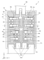
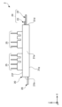
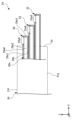
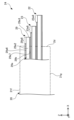
- FIG. 1 is a plan view of a semiconductor module according to a first embodiment
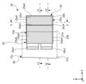
- FIG. 2 is a plan view of the semiconductor unit according to the first embodiment.
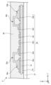
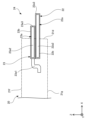
- 1 is a cross-sectional view of a semiconductor unit according to a first embodiment.
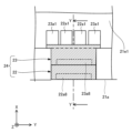
- FIG. 2 is a plan view of a terminal stacking portion according to the first embodiment.
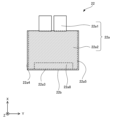
- 4 is a plan view of a first terminal included in the terminal stack of the first embodiment.
- FIG. 4 is a plan view of a second terminal included in the terminal stack portion of the first embodiment.
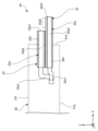
- FIG. FIG. 2 is a cross-sectional view of a terminal stacking portion according to the first embodiment. 4 is a cross-sectional view of the terminal stack portion of the first embodiment from which the bonding area has been removed;
- 5 is a flowchart showing a method for manufacturing a case included in the semiconductor module according to the first embodiment.
- 5A to 5C are diagrams for explaining a covering step included in the manufacturing method of the case of the first embodiment.
- 5A to 5C are diagrams for explaining an oxidation step included in the manufacturing method of the case of the first embodiment.
- 13 is a flowchart showing a method for manufacturing a case included in a semiconductor module according to Modification 1-1 of the first embodiment.
- 11A to 11C are diagrams for explaining a preparation process included in a semiconductor module according to the modification 1-1 of the first embodiment.
- 11A to 11C are diagrams for explaining a terminal forming step and an oxidation step included in the semiconductor module of the modified example 1-1 of the first embodiment.
- FIG. 11 is a cross-sectional view of a terminal stacking portion of a modified example 1-1 of the first embodiment.
- FIG. 11 is a cross-sectional view of a terminal laminated portion from which a bonding region has been removed according to modified example 1-1 of the first embodiment.
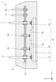
- FIG. FIG. 13 is a perspective view of a semiconductor device according to a second embodiment.
- FIG. 13 is a perspective view of a capacitor according to a second embodiment.
- 13 is a cross-sectional view of a capacitor and a semiconductor module included in a semiconductor device according to a second embodiment.
- FIG. 13 is a perspective view of a semiconductor module according to a third embodiment.
- FIG. 11 is a cross-sectional view of a semiconductor module according to a third embodiment.
- FIG. 13 is a plan view of a semiconductor module according to a third embodiment.
- FIG. 13 is a plan view of a first terminal and a second terminal of the third embodiment.
- FIG. 13 is a cross-sectional view of a first terminal and a second terminal of a third embodiment.
- FIG. 13 is a cross-sectional view of a first terminal and a second terminal of a third embodiment.
- FIG. 13 is a cross-sectional view of a first terminal and a second terminal of a modification 3-1 of the third embodiment.
- 13 is a cross-sectional view of a first terminal, a second terminal, and a third terminal of a modification 3-2 of the third embodiment.
- FIG. 13 is a plan view of a semiconductor module according to a third embodiment.
- FIG. 13 is a plan view of a first terminal and a second terminal of the third embodiment.
- FIG. 13 is a cross-sectional view of a first terminal and a second terminal of a third embodiment.
- FIG. 13 is a cross-sectional view of a first terminal, a second terminal, and a third terminal of a modification 3-3 of the third embodiment.
- FIG. FIG. 13 is a side view of a semiconductor device according to a fourth embodiment.
- FIG. 13 is a plan view of a semiconductor device according to a fourth embodiment.
- FIG. 13 is a cross-sectional view of a semiconductor module according to a fourth embodiment.
- FIG. 13 is a plan view of a bus bar according to a fourth embodiment.
- FIG. 13 is a first cross-sectional view of a bus bar according to a fourth embodiment.
- FIG. 13 is a second cross-sectional view of the bus bar of the fourth embodiment.
- front surface and “upper surface” refer to the X-Y surface facing upward (+Z direction) in the semiconductor device 1 of FIG. 1. Similarly, “upper” refers to the upward (+Z direction) direction in the semiconductor device 1 of FIG. 1.
- rear surface and “lower surface” refer to the X-Y surface facing downward (-Z direction) in the semiconductor device 1 of FIG. 1. Similarly, “lower” refers to the downward (-Z direction) direction in the semiconductor device 1 of FIG. 1. Similar orientations are used in other drawings as necessary.
- “High position” refers to the upper (+Z side) position in the semiconductor device 1 of FIG. 1. Similarly.
- Low position refers to the lower (-Z side) position in the semiconductor device 1 of FIG. 1.
- the terms "front surface”, “upper surface”, “upper”, “rear surface”, “lower surface”, “lower” and “side” are merely convenient expressions for specifying relative positional relationships and do not limit the technical ideas of the present invention.
- “up” and “down” do not necessarily mean the vertical direction relative to the ground. In other words, the directions of “up” and “down” are not limited to the direction of gravity.
- main component refers to a component that contains 80 vol% or more.
- Fig. 1 is a plan view of the semiconductor module according to the first embodiment.
- the semiconductor module 2 has a semiconductor unit (not shown), a heat sink (see FIG. 3) on which the semiconductor unit is disposed, and a case 20 that is disposed on the heat sink and stores the semiconductor unit.
- the semiconductor unit will be described later with reference to FIG. 2 and FIG. 3.
- the case 20 includes a frame portion 21, a terminal stack portion 24, a U terminal 26a, a V terminal 26b, a W terminal 26c, and control terminals 25a, 25b, and 25c.
- the frame portion 21 is generally rectangular in plan view and is surrounded on all four sides by first to fourth side portions 21a to 21d.
- the frame portion 21 includes storage areas 21e1, 21e2, and 21e3 arranged in order along the first side portion 21a and the third side portion 21c on the front surface.
- the storage areas 21e1, 21e2, and 21e3 are partitioned by the control terminals 25a and 25b on the front surface of the frame 21 in a plan view, and are spaces provided along the longitudinal direction (first and third side portions 21a and 21c) of the frame 21.
- the semiconductor units described above are stored in the storage areas 21e1, 21e2, and 21e3.
- the semiconductor units are electrically connected to the first terminal 22 and the second terminal 23, the U terminal 26a, the V terminal 26b, and the W terminal 26c, respectively, included in the terminal stack portion described later, within the storage areas 21e1, 21e2, and 21e3.
- the semiconductor units are electrically connected to the control terminals 25a, 25b, and 25c by wires.
- the sealing member 36 contains a thermosetting resin and a filler contained in the thermosetting resin.
- the thermosetting resin is, for example, an epoxy resin, a phenolic resin, or a maleimide resin.
- the filler is, for example, silicon oxide, aluminum oxide, boron nitride, or aluminum nitride.
- Such a frame portion 21 is formed by injection molding using a thermoplastic resin to include three sets of terminal stacking portions 24, the U terminal 26a, the V terminal 26b, the W terminal 26c, and the control terminals 25a, 25b, and 25c.
- the control terminals 25a, 25b, and 25c may be formed by injection molding using a thermosetting resin separately from the frame portion 21 to be included in the resin.
- the control terminals 25a, 25b, and 25c thus integrally molded from resin may be attached to openings on the front surface of the frame portion 21 to form the storage areas 21e1, 21e2, and 21e3.
- thermoplastic resin is, for example, polyphenylene sulfide (PPS) resin, polybutylene terephthalate (PBT) resin, polybutylene succinate (PBS) resin, polyamide (PA) resin, or acrylonitrile butadiene styrene (ABS) resin.
- PPS polyphenylene sulfide
- PBT polybutylene terephthalate
- PBS polybutylene succinate
- PA polyamide
- ABS acrylonitrile butadiene styrene
- the terminal stacking portion 24 is provided in three sets exposed on the first side portion 21a along the longitudinal direction (first side portion 21a) of the frame portion 21, corresponding to the storage areas 21e1, 21e2, and 21e3, respectively.
- Such terminal stacking portion 24 includes a first terminal 22 and a second terminal 23 stacked on the first terminal 22 with one end of the front surface of the first terminal 22 exposed.
- the front surface of one end of the first terminal 22 is exposed from the first side portion 21a facing upward (in the +Z direction).
- the other end of the first terminal 22 is electrically connected to a location inside the storage area 21e of the case 20 that corresponds to the negative electrode of the semiconductor chip of the semiconductor unit.
- the second terminal 23 is disposed on the first terminal 22 with one end of the first terminal 22 exposed.
- the front surface of one end of the second terminal 23 is exposed facing upward (+Z direction) from the first side portion 21a.
- the other end of the second terminal 23 is electrically connected to a location inside the storage area 21e of the case 20 that corresponds to the positive electrode of the semiconductor chip.
- the first terminal 22 and the second terminal 23 are made of a metal with excellent electrical conductivity.
- a metal is, for example, copper or a copper alloy.
- an oxide film is formed on the surface of each of the first terminal 22 and the second terminal 23. This maintains the insulation of the first terminal 22 and the second terminal 23. Details of such a terminal laminate portion 24 will be described later.
- control terminals 25a, 25b, and 25c extends upward (in the +Z direction) of the semiconductor module 2.
- the other end of each of the control terminals 25a, 25b, and 25c is electrically connected to the control electrodes of the semiconductor chips of the semiconductor units in the storage areas 21e1, 21e2, and 21e3, respectively.
- the control terminals 25a, 25b, and 25c are made of a metal with excellent electrical conductivity. Examples of such metals include copper, copper alloys, aluminum, and aluminum alloys.
- a plating process may be performed. Examples of plating materials used in this case include nickel, nickel-phosphorus alloys, and nickel-boron alloys.
- the U terminal 26a, the V terminal 26b, and the W terminal 26c are exposed on the third side 21c in the longitudinal direction (third side 21c) of the frame 21 in correspondence with the storage areas 21e1, 21e2, and 21e3, respectively.
- the front surfaces of one end of the U terminal 26a, the V terminal 26b, and the W terminal 26c are exposed facing upward (+Z direction) from the third side 21c.
- the other end of the U terminal 26a, the V terminal 26b, and the W terminal 26c are electrically connected to the locations corresponding to the output electrodes of the semiconductor chips of the semiconductor units in the storage areas 21e1, 21e2, and 21e3, respectively.
- the U terminal 26a, the V terminal 26b, and the W terminal 26c are made of a metal with excellent electrical conductivity.
- Such a metal is, for example, copper or a copper alloy.
- a plating process may be performed.
- the plating materials used in this case are, for example, nickel, nickel-phosphorus alloy, and nickel-boron alloy.
- Figure 2 is a plan view of the semiconductor unit of the first embodiment.
- Figure 3 is a cross-sectional view of the semiconductor unit of the first embodiment.
- Figure 3 is a cross-sectional view taken along dashed line Y-Y in Figure 2.
- the semiconductor unit 3 is placed on the heat sink 37 via a bonding member (not shown).
- the case 20 is placed on the heat sink 37 via an adhesive, and the semiconductor unit 3 is stored in the storage areas 21e1, 21e2, and 21e3 of the case 20.
- Such a semiconductor unit 3 includes an insulating circuit board 30, semiconductor chips 34a to 34d, and lead frames 35a to 35d.
- the joining member for joining the heat sink 37 and the semiconductor unit 3 (insulated circuit board 30) is solder or a sintered material.
- the solder used is lead-free solder or lead-containing solder.
- Lead-free solder is mainly composed of an alloy containing at least two of tin, silver, copper, zinc, antimony, indium, and bismuth.
- the solder may further contain additives.
- the additives are, for example, nickel, germanium, cobalt, or silicon.
- the addition of additives to the solder improves the wettability, gloss, and bonding strength, thereby improving reliability.
- Lead-containing solder further contains lead.
- the sintered material used is, for example, a metal material containing at least one of copper, copper alloy, nickel, nickel alloy, silver, and silver alloy.
- the insulating circuit board 30 is rectangular in plan view.
- the insulating circuit board 30 has an insulating plate 31, a metal plate 33 formed on the back surface of the insulating plate 31, and multiple wiring boards 32a-32i formed on the front surface of the insulating plate 31.
- the outer shapes of the multiple wiring boards 32a-32i and the metal plate 33 are smaller than the outer shape of the insulating plate 31 in plan view, and are formed inside the insulating plate 31. Note that the shapes, number, and sizes of the multiple wiring boards 32a-32i are merely examples.
- the insulating plate 31 has a rectangular shape in a plan view.
- the corners of the insulating plate 31 may be chamfered.
- the corners may be C-chamfered or R-chamfered.
- the insulating plate 31 is surrounded on all four sides by the outer periphery, which is made up of long side 31a, short side 31b, long side 31c, and short side 31d.
- Such an insulating plate 31 is made of ceramics with good thermal conductivity.
- the ceramics are made of a material whose main component is, for example, aluminum oxide, aluminum nitride, or silicon nitride.
- the metal plate 33 has a rectangular shape in a plan view. The corners may be, for example, C-chamfered or R-chamfered.
- the metal plate 33 is smaller than the size of the insulating plate 31, and is formed on the entire back surface of the insulating plate 31 except for the edges.
- the metal plate 33 is mainly composed of a metal with excellent thermal conductivity.
- the metal is, for example, copper, aluminum, or an alloy containing at least one of these.
- a plating process may be performed to improve the corrosion resistance of the metal plate.
- the plating material used is, for example, nickel, a nickel-phosphorus alloy, or a nickel-boron alloy.
- the wiring boards 32a to 32i are formed over the entire surface of the insulating plate 31 except for the edges.
- the ends of the wiring boards 32a to 32f that face the outer periphery of the insulating plate 31 overlap with the end of the metal plate 33 on the outer periphery side of the insulating plate 31.
- the insulating circuit board 30 maintains a stress balance with the metal plate 33 on the back surface of the insulating plate 31. Damage such as excessive warping and cracking of the insulating plate 31 is suppressed.
- the wiring boards 32a to 32i are made of a metal with excellent electrical conductivity. Such a metal is, for example, copper, aluminum, or an alloy containing at least one of these.
- the surfaces of the wiring boards 32a to 32i may be plated to improve corrosion resistance.
- the plating material used is, for example, nickel, a nickel-phosphorus alloy, or a nickel-boron alloy.
- Wiring board 32a is formed on the long side 31a of insulating board 31, along long side 31a, from short side 31b to short side 31d.
- a recess is formed on the long side 31c side of wiring board 32a on the lower side (-X direction).
- Wiring board 32b is almost linearly symmetrical with wiring board 32a about the center line in the ⁇ Y direction.
- Wiring board 32b is formed on the long side 31c of insulating board 31, along long side 31c, from short side 31b to short side 31d.
- a recess is formed on the long side 31a side of wiring board 32b on the lower side (-X direction).
- Wiring board 32c is disposed in a region surrounded by the lower part (-X direction) of wiring board 32a, the lower part (-X direction) of wiring board 32e, short side 31d, and wiring board 32e. That is, wiring board 32c is approximately L-shaped.
- Wiring board 32d is approximately linearly symmetrical with wiring board 32c about the center line in the ⁇ Y directions.
- Wiring board 32d is disposed in a region surrounded by the lower part (-X direction) of wiring board 32b, wiring board 32f, short side 31d, and wiring board 32f. That is, wiring board 32d is approximately L-shaped.
- Wiring board 32g is I-shaped in plan view and is disposed between wiring boards 32e and 32f along long sides 31a and 31c.
- Wiring board 32h is I-shaped in plan view and is disposed on the wiring board 32e side along long side 31a in the area surrounded by the recesses of wiring boards 32e and 32f.
- Wiring board 32i is L-shaped in plan view and is disposed on the wiring board 32f side along long side 31c in the area surrounded by the recesses of wiring boards 32e and 32f.
- Wiring board 32i is disposed so as to surround the long side 31c and short side 31d of wiring board 32h.
- the second connection portion 23a1 of the second terminal 23 is joined to the lower ends (-X direction) of the wiring boards 32a and 32b of the insulating circuit board 30.
- the first connection portion 22a1 of the first terminal 22 is joined to the lower ends (-X direction) of the wiring boards 32c and 32d of the insulating circuit board 30.
- the joints between the U terminal 26a, the V terminal 26b, and the W terminal 26c are joined to the upper ends (+X direction) of the wiring boards 32e and 32f of the insulating circuit board 30.
- FIG. 2 illustrates an example in which the U terminal 26a is joined to the wiring boards 32e and 32f.
- an insulating circuit board 30 having such a configuration, a DCB (Direct Copper Bonding) board or an AMB (Active Metal Brazed) board may be used.
- the insulating circuit board 30 dissipates heat generated in the semiconductor chips 34a to 34d (described later) by conducting it to the back side of the insulating circuit board 30 via the wiring boards 32a, 32b, 32e, and 32f, the insulating plate 31, and the metal plate 33.
- Semiconductor chips 34a to 34d are power devices made of silicon carbide.
- a power device is a power MOSFET (Metal Oxide Semiconductor Field Effect Transistor).
- the body diode functions as an FWD (Free Wheeling Diode).
- Each of these semiconductor chips 34a to 34d has a drain electrode as an input electrode (main electrode) on the back surface, and a gate electrode as a control electrode and a source electrode as an output electrode (main electrode) on the front surface.
- the semiconductor chips 34a to 34d may also be power devices made of silicon.
- the power device may be, for example, an RC (Reverse Conducting)-IGBT (Insulated Gate Bipolar Transistor).
- An RC-IGBT is a device in which an IGBT, which is a switching element, and an FWD, which is a diode element, are configured within a single chip.
- Each of these semiconductor chips 34a to 34d has, for example, a collector electrode on the back surface as an input electrode (main electrode), a gate electrode on the front surface as a control electrode, and an emitter electrode on the front surface as an output electrode (main electrode).
- multiple semiconductor chips 34a to 34d are arranged on each of wiring boards 32a, 32b, 32e, and 32f via the bonding members described above.
- Figure 2 shows a case where two chips are arranged on each of the wiring boards. In this case, semiconductor chips 34a to 34d are arranged so that their control electrodes face each other.
- Lead frames 35a to 35d electrically connect output electrodes on the front surfaces of semiconductor chips 34a to 34d to wiring boards 32e, 32f, 32c, and 32d.
- Lead frame 35a electrically and mechanically connects semiconductor chip 34a to wiring board 32e.
- Lead frame 35b electrically and mechanically connects semiconductor chip 34b to wiring board 32f.
- Lead frame 35c electrically and mechanically connects semiconductor chip 34c to wiring board 32c.
- Lead frame 35d electrically and mechanically connects semiconductor chip 34d to wiring board 32d.
- lead frames 35a to 35d One end of the lead frames 35a to 35d is joined to the output electrodes of the semiconductor chips 34a to 34d using the solder described above as a joining material.
- the other end of the lead frames 35a to 35d is joined to the wiring boards 32e, 32f, 32c, and 32d using the joining material described above. Alternatively, they may be joined by ultrasonic or laser welding.
- Such lead frames 35a to 35d are made of a material with excellent conductivity. Examples of such materials include copper, aluminum, or an alloy containing at least one of these.
- the surfaces of the lead frames 35a to 35d may be plated to improve corrosion resistance. In this case, the plating material is, for example, nickel, a nickel-phosphorus alloy, or a nickel-boron alloy.
- the heat sink 37 has a rectangular shape in a plan view, and corresponds to the outline of the rear surface of the case 20.
- the semiconductor units 3 are joined to the front surface of the heat sink 37 along the longitudinal direction by respective joining members.
- the heat sink 37 is mainly composed of a metal with excellent thermal conductivity.
- the metal is, for example, copper, aluminum, or an alloy containing at least one of these.
- a plating process may be performed to improve the corrosion resistance of the metal plate.
- the plating material used is, for example, nickel, a nickel-phosphorus alloy, or a nickel-boron alloy.
- Fig. 4 is a plan view of the terminal stack of the first embodiment.
- Fig. 5 is a plan view of a first terminal included in the terminal stack of the first embodiment, and
- Fig. 6 is a plan view of a second terminal included in the terminal stack of the first embodiment.
- Fig. 7 is a cross-sectional view of the terminal stack of the first embodiment, and
- Fig. 8 is a cross-sectional view of the terminal stack of the first embodiment from which the bonding region has been removed.
- Figs. 7 and 8 show cross-sectional views taken along dashed line Y-Y in Fig. 4.
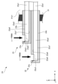
- the terminal stacking portion 24 includes a first terminal 22 and a second terminal 23. As shown in FIG. 7, in the terminal stacking portion 24, a flat second terminal 23 is stacked on a flat first terminal 22. In this case, the tip surface 22a3 included in the first terminal 22 extends outward (in the -X direction) beyond the tip surface 23a3 included in the second terminal 23, exposing an area corresponding to the first bonding region 22a8 included in the first terminal 22. In addition, the terminal stacking portion 24 is fixed to the frame portion 21 with the tip surface 22a3 of the first terminal 22 being flush with the first side portion 21a of the frame portion 21.
- the first terminal 22 includes a first conductive plate 22a and a first oxide film 22b.
- the first conductive plate 22a integrally includes a first connection portion 22a1 and a first wiring portion 22a2.
- the first oxide film 22b covers the surface of the first wiring portion 22a2.
- the first wiring portion 22a2 is a rectangular portion represented by a dashed line in the first oxide film 22b in FIG. 5.
- the first wiring portion 22a2 is flat and includes a tip surface 22a3, first side surfaces 22a4 and 22a5, a first front surface 22a6, and a first back surface 22a7.
- the first front surface 22a6 and the first back surface 22a7 are rectangular in plan view and have the same size.
- a first bonding area 22a8 is set on the outside (-X direction) of the first front surface 22a6 along the tip surface 22a3 in plan view.
- the first bonding area 22a8 is an area surrounded by a dashed line on the -X direction side of the first front surface 22a6 in FIG. 5.
- the range of the first bonding area 22a8 corresponds to the range where the first, second, and third connection parts 43a, 43b, and 43c of the first connection terminal 43 included in the capacitor 4 described later are bonded.
- the first bonding area 22a8 is rectangular in plan view.
- the width of the first bonding area 22a8 in the ⁇ Y direction is smaller than the width of the first front surface 22a6 in the same direction.
- the first bonding area 22a8 has a predetermined length inward (+X direction) from the tip surface 22a3.
- the tip surface 22a3 is the outermost end in the extension direction (-X direction) of the terminal laminated portion 24. In other words, the tip surface 22a3 is provided in the -X direction on all four sides of the first front surface 22a6 and the first back surface 22a7. The tip surface 22a3 is approximately parallel to the first side portion 21a and the third side portion 21c of the frame portion 21 of the case 20.
- the first side surfaces 22a4 and 22a5 are provided on the four sides of the first front surface 22a6 and the first back surface 22a7 in the ⁇ Y direction.
- the first side surfaces 22a4 and 22a5 are connected to the first front surface 22a6 and the first back surface 22a7 from the ends of the four sides of the first front surface 22a6 and the first back surface 22a7 in the ⁇ Y direction.
- the first side surfaces 22a4 and 22a5 are parallel to the extension direction (+X direction) of the terminal stacking portion 24.
- the first side surfaces 22a4 and 22a5 are approximately parallel to the second side portion 21b and the fourth side portion 21d of the frame portion 21 of the case 20.
- the rear end surface (reference numerals omitted) facing the tip surface 22a3 is provided on the four sides of the first front surface 22a6 and the first back surface 22a7 in the +X direction.
- the first connection portion 22a1 has a rectangular shape in a plan view.
- the first connection portion 22a1 has the same thickness as the first wiring portion 22a2.
- the first connection portion 22a1 is formed on the rear end surface opposite the tip surface 22a3 of the first wiring portion 22a2, and extends a predetermined length in the +X direction.
- the two first connection portions 22a1 are lined up at the center of the rear end surface of the first wiring portion 22a2 with a predetermined gap in the ⁇ Y direction.
- the first conductive plate 22a is made of a metal with excellent electrical conductivity. Such a metal is, for example, copper or an alloy mainly composed of copper.
- the thickness of the first conductive plate 22a is generally uniform overall, and is, for example, 0.8 mm or more and 1.2 mm or less, e.g., 1.0 mm.
- the first oxide film 22b is provided on the surface of the first wiring portion 22a2 of the first conductive plate 22a. That is, the first oxide film 22b is provided on the front end surface 22a3, the first side surfaces 22a4 and 22a5, the first front surface 22a6, and the first back surface 22a7 of the first wiring portion 22a2.
- the first oxide film 22b may be formed on the rear end surface opposite the front end surface 22a3 of the first conductive plate 22a.
- the first oxide film 22b is not provided on the first connection portion 22a1 of the first conductive plate 22a.
- Such a first oxide film 22b is mainly composed of an insulating material. This material is a metal oxide, for example, an aluminum oxide layer.
- the first oxide film 22b is illustrated as a single layer.
- An aluminum layer may be included on the surface of the first conductive plate 22a corresponding to the first oxide film 22b of the aluminum oxide layer.
- the second terminal 23 includes a second conductive plate 23a and a second oxide film 23b.
- the second conductive plate 23a integrally includes a second connection portion 23a1 and a second wiring portion 23a2.
- the second oxide film 23b covers the surface of the second wiring portion 23a2.
- the second wiring portion 23a2 is a T-shaped portion represented by a dashed line in the second oxide film 23b in FIG. 6.
- the second wiring portion 23a2 is flat and includes a tip surface 23a3, second side surfaces 23a4 and 23a5, a second front surface 23a6, and a second back surface 23a7.
- the second front surface 23a6 and the second back surface 23a7 are T-shaped in a plan view and are the same size.
- a second bonding area 23a8 is set on the outside (-X direction) of the second front surface 23a6 along the tip surface 23a3 in a plan view.
- the second bonding area 23a8 is an area surrounded by a dashed line on the -X direction side of the second front surface 23a6 in FIG. 6, and faces the first bonding area 22a8.
- the range of the second bonding area 23a8 corresponds to the size of the connecting members 41a, 41b, and 41c included in the capacitor 4 described later.
- the second bonding area 23a8 is rectangular in a plan view.
- the width of the second bonding area 23a8 in the ⁇ Y direction is smaller than the width of the second front surface 23a6 in the same direction.
- the second bonding area 23a8 has a predetermined length inward (+X direction) from the tip surface 23a3.
- the tip surface 23a3 is the outermost end in the extension direction (-X direction) of the terminal stacking portion 24. In other words, the tip surface 23a3 is provided in the -X direction on all four sides of the second front surface 23a6 and the second back surface 23a7. The tip surface 23a3 is approximately parallel to the first side portion 21a and the third side portion 21c of the frame portion 21 of the case 20.
- the second side surfaces 23a4 and 23a5 are provided on the four sides of the second front surface 23a6 and the second back surface 23a7 in the ⁇ Y direction.
- the second side surfaces 23a4 and 23a5 are continuous from the ends of the four sides of the second front surface 23a6 and the second back surface 23a7 in the ⁇ Y direction to the second front surface 23a6 and the second back surface 23a7.
- the second side surfaces 23a4 and 23a5 are parallel to the extension direction (-X direction) of the terminal stacking portion 24.
- the second side surfaces 23a4 and 23a5 are approximately parallel to the second side portion 21b and the fourth side portion 21d of the frame portion 21 of the case 20.
- the rear end surface (reference numerals omitted) facing the tip surface 23a3 is provided on the four sides of the second front surface 23a6 and the second back surface 23a7 in the +X direction.
- the second connection portion 23a1 has a rectangular shape in a plan view.
- the second connection portion 23a1 has the same thickness as the second wiring portion 23a2.
- the second connection portion 23a1 is formed on the rear end surface opposite the tip surface 23a3 of the second wiring portion 23a2, and extends a predetermined length in the +X direction.
- the two second connection portions 23a1 are formed on both ends of the rear end surface of the second wiring portion 23a2 in the ⁇ Y direction.
- the second connection portion 23a1 may have the same thickness and size as the first connection portion 22a1. When the second terminal 23 is placed on the first terminal 22, the second connection portion 23a1 is located outside the first connection portion 22a1, as shown in FIG. 4.
- the second conductive plate 23a is made of a metal with excellent electrical conductivity.
- a metal is, for example, copper or an alloy mainly composed of copper.
- the thickness of the first conductive plate 22a is generally uniform and is, for example, 0.8 mm or more and 1.2 mm or less, e.g., 1.0 mm.
- the second oxide film 23b is provided on the surface of the second wiring portion 23a2 of the second conductive plate 23a. That is, the second oxide film 23b is formed on the tip surface 23a3, the second side surfaces 23a4 and 23a5, the second front surface 23a6, and the second back surface 23a7 of the second wiring portion 23a2.
- the second oxide film 23b may be provided on the rear end surface opposite the tip surface 23a3 of the second conductive plate 23a.
- the second oxide film 23b is not provided on the second connection portion 23a1 of the second conductive plate 23a.
- Such a second oxide film 23b is formed of the same material as the first oxide film 22b. Even in this case, an aluminum layer may be included on the surface of the second conductive plate 23a corresponding to the second oxide film 23b of the aluminum oxide layer.
- terminal laminated portion 24 is molded integrally with frame portion 21. As shown in FIG. 7, the portion of terminal laminated portion 24 corresponding to first wiring portion 22a2 included in first terminal 22 and the portion corresponding to second wiring portion 23a2 included in second terminal 23 are fixed to frame portion 21. First connection portion 22a1 of first terminal 22 and second connection portion 23a1 of second terminal 23 are disposed within storage area 21e of frame portion 21.
- the first connection portion 22a1 of the first terminal 22 is joined to the wiring boards 32c and 32d of the insulating circuit board 30 stored in the storage area 21e, and is electrically connected to the output electrodes (negative electrodes) of the semiconductor chips 34c and 34d (see FIG. 2).
- the second connection portion 23a1 of the second terminal 23 is joined to the wiring boards 32a and 32b of the insulating circuit board 30 stored in the storage area 21e, and is electrically connected to the input electrodes (positive electrodes) of the semiconductor chips 34a and 34b (see FIG. 2).
- the first connection portion 22a1 and the second connection portion 23a1 are joined, for example, by ultrasonic bonding, laser welding, or a bonding material (for example, solder or sintered body).
- the first terminal 22 and the second terminal 23 of the terminal laminate 24 are laminated via the first oxide film 22b and the second oxide film 23b. Therefore, the insulation between the first conductive plate 22a of the first terminal 22 and the second conductive plate 23a of the second terminal 23 is maintained. Therefore, the thickness of the first oxide film 22b and the second oxide film 23b is a thickness that can secure the creeping distance between the first terminal 22 and the second terminal 23 and sufficiently maintain the insulation. For example, when the dielectric breakdown voltage between the first terminal 22 and the second terminal 23 is 1 kV or more, the combined thickness of the first oxide film 22b and the second oxide film 23b between the first terminal 22 and the second terminal 23 is 20 ⁇ m or more. The method of coating the first conductive plate 22a and the second conductive plate 23a with the first oxide film 22b and the second oxide film 23b will be described in detail later.
- first oxide film 22b and the second oxide film 23b may be provided.
- first oxide film 22b may be provided on at least the first side surfaces 22a4, 22a5 and the first front surface 22a6.
- second oxide film 23b may be provided on the second side surfaces 23a4, 23a5 and the second back surface 23a7.
- an insulating member In order to maintain the insulation between the first conductive plate 22a and the second conductive plate 23a, an insulating member must be provided between the first wiring portion 22a2 of the first conductive plate 22a and the second wiring portion 23a2 of the second conductive plate 23a. If the insulating member is, for example, a sheet-shaped insulating paper, a sufficient creepage distance can be secured between the first terminal 22 (first conductive plate 22a) and the second terminal 23 (second conductive plate 23a), and the insulation between the first terminal 22 and the second terminal 23 can be maintained.
- insulating paper has low moisture resistance. For this reason, after a long period of use, it becomes impossible to maintain the insulation between the first terminal 22 and the second terminal 23.
- the insulating paper may include thin portions. In such portions, there is a risk of insulation breakdown due to the voltage between the first terminal 22 and the second terminal 23.
- the first oxide film 22b and the second oxide film 23b are used as insulating members between the first wiring portion 22a2 of the first conductive plate 22a and the second wiring portion 23a2 of the second conductive plate 23a. This improves moisture resistance. Therefore, even if the period of use becomes long, deterioration of the insulation between the first terminal 22 and the second terminal 23 can be suppressed.
- the adhesion between the first oxide film 22b and the second oxide film 23b, which are oxide layers, and the thermoplastic resin that constitutes the frame portion 21 is better than when insulating paper is used. This improves the adhesion between the terminal stack portion 24 and the case 20.
- the first oxide film 22b and the second oxide film 23b, which are oxide layers, are less likely to cause dielectric breakdown than when insulating paper is used.
- the insulation between the first conductive plate 22a and the second conductive plate 23a is maintained by the first oxide film 22b and the second oxide film 23b, a separate insulating material is not required between the first terminal 22 and the second terminal 23. This makes it possible to miniaturize the terminal stack 24, and thus the semiconductor module 2 can be miniaturized.
- a positive terminal is joined to the first joint region 22a8 of the first terminal 22, and a negative terminal is joined to the second joint region 23a8 of the second terminal 23. Then, the current flows in the first terminal 22 and the second terminal 23 in the opposite directions.
- the length in the thickness direction between the first terminal 22 and the second terminal 23 can be shortened, so that the inductance reduction effect is further enhanced, and the inductance between the first terminal 22 and the second terminal 23 can be further reduced.
- the first connection terminal 43 and the linking member 41 are respectively joined to the first terminal 22 and the second terminal 23 of the terminal stack 24 as described later (see FIG. 14 described later).
- the first oxide film 22b corresponding to the first bonding area 22a8 of the first terminal 22 is irradiated with a laser, for example.
- the second oxide film 23b corresponding to the second bonding area 23a8 of the second terminal 23 is irradiated with a laser.
- the first oxide film 22b is removed and the first bonding area 22a8 of the first conductive plate 22a is exposed.
- the second oxide film 23b is removed and the second bonding area 23a8 of the second conductive plate 23a is exposed.
- the first oxide film 22b and the second oxide film 23b may be removed by, for example, grinding with a file or cutting with a milling cutter.
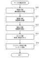
- FIG. 9 is a flow chart showing a method for manufacturing the case included in the semiconductor module of the first embodiment. Note that the method for manufacturing the case 20 shown in FIG. 9 is included in the method for manufacturing the semiconductor module 2.
- step S10 materials, tools, parts, etc. necessary for manufacturing the case 20 are also prepared as necessary.
- the various terminals are the first terminal 22, the second terminal 23, the U terminal 26a, the V terminal 26b, the W terminal 26c, and the control terminal 25.
- the first conductive plate 22a and the second conductive plate 23a in Figs. 5 and 6, and the U terminal 26a, the V terminal 26b, and the W terminal 26c in Fig. 1 are obtained from the conductive plate.
- the terminals are obtained, for example, by punching, cutting, or stamping the conductive plate.
- the conductive plate is made of a metal with excellent conductivity, such as copper or an alloy mainly composed of copper.
- the case material is, for example, PPS resin.
- Step S11 a coating process is performed to coat the first conductive plate 22a and the second conductive plate 23a with a coating layer (step S11).
- the first terminal 22 and the second terminal 23 shown in Figures 4 and 5 can be manufactured by several methods.
- Step S11 and the next step S12 are one example of a manufacturing method.
- Figure 10 is a diagram for explaining the coating process included in the manufacturing method of the case of the first embodiment. Note that Figure 10 describes the first conductive plate 22a. The second conductive plate 23a is processed in the same manner.
- the coating container 50 is filled with the solution 51.
- the solution 51 contains, for example, aluminum.
- the aluminum-containing solution 51 may further contain magnesium or silicon.
- the first conductive plate 22a is moved vertically downward (toward the solution 51) with the tip surface 22a3 facing downward with respect to the solution 51 in the coating container 50.
- the first wiring portion 22a2 is immersed in the solution 51, leaving the first connection portion 22a1 of the first conductive plate 22a.
- the tip surface 22a3, the first side surfaces 22a4 and 22a5, the first front surface 22a6, and the first back surface 22a7 (see FIG. 7) of the first wiring portion 22a2 of the first conductive plate 22a come into contact with the solution 51.
- the rear end surface of the first wiring portion 22a2 opposite to the tip surface 22a3 may also come into contact with the solution 51.
- the first connection portion 22a1 of the first conductive plate 22a does not come into contact with the solution 51.
- the second conductive plate 23a is similarly configured such that, except for the second connection portion 23a1, the tip surface 23a3, the second side surfaces 23a4 and 23a5, the second front surface 23a6, and the second back surface 23a7 of the second wiring portion 23a2 of the second conductive plate 23a come into contact with the solution 51.
- the second connection portion 23a1 of the second conductive plate 23a does not come into contact with the solution 51.
- the rear end surface of the second wiring portion 23a2 opposite the tip surface 22a3 may also come into contact with the solution 51.
- the coating layer 22b1 contains aluminum.
- the second conductive plate 23a has a coating layer provided on the tip surface 23a3, the second side surfaces 23a4 and 23a5, the second front surface 23a6, and the second back surface 23a7 of the second wiring portion 23a2 included in the second conductive plate 23a.
- the above method is merely one example of a method for coating the first conductive plate 22a and the second conductive plate 23a with a coating layer containing aluminum.
- Other methods may be used as long as they can coat the first conductive plate 22a and the second conductive plate 23a with a coating layer containing aluminum. Examples of such methods include sputtering, vapor deposition, and plating.
- an oxidation step is performed to oxidize the coating layers of the first conductive plate 22a and the second conductive plate 23a (step S12).
- an anodizing process is performed.
- the anodizing process is a process in which a conductive plate is electrically oxidized by passing a current directly through the conductive plate as the anode in an electrolytic solution, thereby forming an oxide layer on the surface.
- the oxidation process using such an anodizing process is described with reference to FIG. 11.
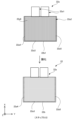
- FIG. 11 is a diagram for explaining the oxidation process included in the manufacturing method of the case of the first embodiment. Note that FIG. 11 describes the first conductive plate 22a.
- the second conductive plate 23a is also processed in the same manner.
- the first conductive plate 22a (the upper part of FIG. 11) coated with the coating layer 22b1 is immersed in an electrolytic solution.
- the electrolytic solution also contains a cathode.
- the cathode may be composed mainly of, for example, lead and carbon.
- the electrolytic solution may be, for example, an aqueous solution of oxalic acid, chromic acid, phosphoric acid, or the like. In this example, an aqueous solution of oxalic acid is used as the electrolytic solution.
- the oxide film formed by the anodizing method using an aqueous solution of oxalic acid has a thick barrier layer, small micropores, and a high dielectric breakdown voltage.
- the thickness of the oxide layer formed must be 20 ⁇ m or more.
- an oxide layer of a thickness that achieves such a dielectric breakdown voltage can be formed.
- a positive electrode is applied to the first conductive plate 22a, and a negative electrode is applied to the cathode, and a direct current is passed for a predetermined time.
- the coating layer 22b1 that coats the surface of the first wiring portion 22a2 of the first conductive plate 22a is oxidized, and a first oxide film 22b (the lower diagram in FIG. 11) is formed.
- the first oxide film 22b is formed on the tip surface 22a3, the first side surfaces 22a4 and 22a5, the first front surface 22a6, and the first back surface 22a7 of the first wiring portion 22a2 of the first conductive plate 22a.
- the second oxide film 23b is formed on the tip surface 23a3, the second side surfaces 23a4 and 23a5, the second front surface 23a6, and the second back surface 23a7 of the second wiring portion 23a2 of the second conductive plate 23a for the second terminal 23.
- the first oxide film 22b and the second oxide film 23b are composed mainly of aluminum oxide, for example.
- the first oxide film 22b and the second oxide film 23b are illustrated as a single layer. Note that an aluminum layer may remain on the surface of the first wiring portion 22a2 of the first conductive plate 22a and the second wiring portion 23a2 of the second conductive plate 23a, and the first oxide film 22b and the second oxide film 23b may be formed on top of the aluminum layer. In this manner, the first terminal 22 and the second terminal 23 are obtained.
- the first oxide film 22b is formed on the tip surface 22a3, the first side surface 22a4, 22a5, the first front surface 22a6, and the first back surface 22a7 of the first wiring portion 22a2, leaving only the first connection portion 22a1, in the first terminal 22.
- the second oxide film 23b is formed on the tip surface 23a3, the second side surface 23a4, 23a5, the second front surface 23a6, and the second back surface 23a7 of the second wiring portion 23a2, leaving only the second connection portion 23a1, in the second terminal 23. If the creepage distance between the first conductive plate 22a and the second conductive plate 23a can be secured and sufficient insulation can be maintained, only the first oxide film 22b or only the second oxide film 23b may be provided.
- the first oxide film 22b may be provided only on the first front surface 22a6 and the first side surfaces 22a4 and 22a5.
- the second oxide film 23b may be provided only on the second back surface 23a7 and the second side surfaces 23a4 and 23a5.
- the first oxide film 22b may be provided only on the first front surface 22a6 and the first side surfaces 22a4 and 22a5, so that the second oxide film 23b may be provided only on the second back surface 23a7 and the second side surfaces 23a4 and 23a5.
- the area corresponding to the first bonding region 22a8 of the first oxide film 22b is removed by a laser. Instead of such removal, the first bonding region 22a8 on the first front surface 22a6 of the first conductive plate 22a may be masked in advance in step S11 so as not to come into contact with the solution 51.
- a mask made of a material having a higher melting point than aluminum is used to mask the portion corresponding to the first bonding region 22a8 of the first conductive plate 22a. This prevents the solution 51 from coming into contact with the portion.
- step S12 is performed with the first bonding region 22a8 of the first conductive plate 22a masked. At this time, no coating layer is formed in the area covered by the mask. Then, by removing the mask, the first bonding region 22a8 is opened on the first front surface 22a6 of the first terminal 22, and the first oxide film 22b can be formed. Similarly, for the second terminal 23, the second bonding region 23a8 is opened and the second oxide film 23b can be formed.
- a setting process is performed to set the parts in the mold for the case (step S13).
- the parts are the first terminal 22, the second terminal 23, the U terminal 26a, the V terminal 26b, the W terminal 26c, and the control terminal.
- the terminal stack section 24 which is configured by placing the second terminal 23 on the first terminal 22, is set.
- step S14 an insert molding process is performed in which case material is filled into the mold for such a case.
- the case material is filled into the mold in which the parts were set in step S13, and the case material is hardened.
- the case material here is, for example, PPS resin. After the case material has hardened, the mold is removed, and the case 20 shown in FIG. 1 is obtained.
- the case 20 manufactured in this manner is set on the heat sink 37 to which the semiconductor unit 3 is bonded. At this time, the semiconductor unit 3 is stored in the storage areas 21e1, 21e2, and 21e3 of the case 20. A wiring process is performed to electrically connect the semiconductor unit 3 to various terminals of the case 20, and a sealing material is filled in the storage areas 21e1, 21e2, and 21e3, thereby obtaining the semiconductor module 2.
- the semiconductor module 2 includes a first conductive plate 22a mainly composed of copper or a copper alloy, a second conductive plate having a second back surface 23a7 facing the first conductive plate 22a and a side surface continuing from the second back surface 23a7 and mainly composed of copper or a copper alloy, and a second oxide film 23b provided on the back surface and side surface of the second conductive plate, which is electrically insulating and contains a metal oxide of an element different from the metal of the second conductive plate 23a.
- the first oxide film 22b and the second oxide film 23b are used as insulating members between the first wiring portion 22a2 of the first conductive plate 22a and the second wiring portion 23a2 of the second conductive plate 23a. This can improve moisture resistance. Therefore, even if the period of use becomes long, the deterioration of the insulation between the first terminal 22 and the second terminal 23 can be suppressed.
- the adhesion between the first oxide film 22b and the second oxide film 23b and the thermoplastic resin that constitutes the frame portion 21 is better than when insulating paper is used. This improves the adhesion between the terminal stack portion 24 and the case 20. Furthermore, the first oxide film 22b and the second oxide film 23b are less likely to cause dielectric breakdown than when insulating paper is used.
- the insulation between the first conductive plate 22a and the second conductive plate 23a is maintained by the first oxide film 22b and the second oxide film 23b, a separate insulating material is not required between the first terminal 22 and the second terminal 23. This makes it possible to miniaturize the terminal stack 24, and thus the semiconductor module 2 can be miniaturized.
- a positive terminal is joined to the first joint region 22a8 of the first terminal 22, and a negative terminal is joined to the second joint region 23a8 of the second terminal 23. Then, the current flows in the first terminal 22 and the second terminal 23 in the opposite directions.
- the length in the thickness direction between the first terminal 22 and the second terminal 23 can be shortened, so the inductance reduction effect is further enhanced, and the inductance between the first terminal 22 and the second terminal 23 can be further reduced.
- the first conductive plate 22a and the second conductive plate 23a are immersed in a solution 51 containing aluminum to adhere a coating layer to the surfaces of the first conductive plate 22a and the second conductive plate 23a, and the coating film is oxidized by anodization.
- a clad material is used for the first conductive plate 22a and the second conductive plate 23a.
- the semiconductor module 2 of modified example 1-1 includes a terminal stack 24 that uses a clad material.
- the semiconductor module 2 of modified example 1-1 is similar to the first embodiment except for the terminal stack 24.
- FIG. 12 is a flowchart showing the manufacturing method of the case included in the semiconductor module of the modified example 1-1 of the first embodiment.
- the manufacturing method of the case 20 shown in FIG. 12 is included in the manufacturing method of the semiconductor module 2.
- the explanation of the same steps as in the flowchart of FIG. 9 will be simplified.
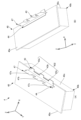
- FIG. 13 is a diagram for explaining the preparation process included in the semiconductor module of modified example 1-1 of the first embodiment. Note that, for the clad material 22c, FIG. 13(A) is a plan view, FIG. 13(B) is a side view as seen in the +X direction, and FIG. 13(C) is a side view as seen in the -Y direction.
- the clad material 22c includes a conductive plate 22c2 and a clad film 22c1 formed on the front and back surfaces of the conductive plate 22c2.
- the conductive plate 22c2 is the base material of the clad material 22c, and is copper or an alloy mainly composed of copper, similar to the first conductive plate 22a of the first embodiment.
- the clad film 22c1 is mainly composed of aluminum.
- the clad material 22c is formed by providing the clad film 22c1 on the front and back surfaces of the conductive plate and rolling it under pressure.
- the metal of the conductive plate 22c2 and the metal of the clad film 22c1 are joined by roll bonding in which interatomic bonding is performed by pressure, without using a bonding material. Therefore, the clad film 22c1 is not easily peeled off from the conductive plate 22c2.
- FIG. 14 is a diagram for explaining the terminal forming process and the oxidation process included in the semiconductor module of modified example 1-1 of the first embodiment.
- FIG. 14(A) is a plan view showing the state after the terminal forming process.
- FIG. 14(B) is a plan view showing the state after the oxidation process described below.
- the clad material 22c prepared in step S10 is pressed (sheared) to correspond to the shapes of the first conductive plate 22a and the second conductive plate 23a of the first embodiment.
- the clad material 22c pressed in this manner has a shape as shown in FIG. 14(A).
- a clad film 22c1 is formed on the front and back surfaces of the first conductive plate 22a.
- a clad film is also formed on the front and back surfaces of the second conductive plate 23a.
- an oxidation step is performed to oxidize the clad film 22c1 of the first conductive plate 22a (step S12).
- an anodizing process is performed as in the first embodiment.
- the clad film 22c1 on the front and back surfaces of the first conductive plate 22a is oxidized to become the first oxide film 22a2, and the first terminal 22 is obtained.
- a first oxide film 22a2 is formed on the front and back surfaces of the first connection portion 22a1.
- the first oxide film 22a2 on the first connection portion 22a1 may be removed. By removing it, the first terminal 22 shown in FIG. 14(B) is obtained.
- the second terminal 23 can also be obtained in a similar manner.
- the clad material 22c is prepared in the preparation step of step S10, and the terminal forming step of step S11a and the oxidation step of step S12 are performed on this clad material 22c.
- the first terminal 22 may be prepared by performing the terminal forming step and the oxidation step on the clad material 22c in the preparation step of step S10. The same applies to the second terminal 23.
- FIG. 15 is a cross-sectional view of the terminal stacking portion of the modified example 1-1 of the first embodiment
- FIG. 16 is a cross-sectional view of the terminal stacking portion of the modified example 1-1 of the first embodiment from which the bonding region has been removed. Note that FIG. 15 and FIG. 16 correspond to FIG. 7 and FIG. 8 of the first embodiment.
- the terminal stack 24 of the modified example 1-1 also includes a first terminal 22 and a second terminal 23, as shown in FIG. 15.
- a flat second terminal 23 is stacked on a flat first terminal 22.
- the tip surface 22a3 included in the first terminal 22 extends outward (in the -X direction) beyond the tip surface 23a3 included in the second terminal 23, exposing an area corresponding to the first bonding region 22a8 included in the first terminal 22.
- the terminal stack 24 is fixed to the frame 21 with the tip surface 22a3 of the first terminal being flush with the first side 21a of the frame 21.
- the first terminal 22 includes a first conductive plate 22a and a first oxide film 22b, as in the case of FIG. 7 of the first embodiment. As described above, the first terminal 22 is obtained from the clad material 22c. Therefore, the first oxide film 22b is formed only on the front surface 22a6 and back surface 22a7 of the first wiring portion 22a2 of the first conductive plate 22a. The first oxide film 22b is not formed on the leading end surface 22a3, the rear end surface (reference numerals omitted), and the first side surfaces 22a4 and 22a5 of the first wiring portion 22a2 of the first conductive plate 22a.
- the second terminal 23 also includes a second conductive plate 23a and a second oxide film 23b, as in the case of FIG. 7 of the first embodiment. As described above, the second terminal 23 is also obtained from the clad material 22c. Therefore, the second oxide film 23b is formed only on the front surface 23a6 and back surface 23a7 of the second wiring portion 23a2 of the second conductive plate 23a. The second oxide film 23b is not formed on the tip surface 23a3, rear end surface (reference numerals omitted), and second side surfaces 23a4 and 23a5 of the second wiring portion 23a2 of the second conductive plate 23a.
- the first oxide film 22b and the second oxide film 23b are not formed on the tip surfaces 22a3, 23a3, the first side surfaces 22a4, 22a5, the second side surfaces 23a4, 23a5, and the rear end surfaces of the first conductive plate 22a and the second conductive plate 23a of both the first terminal 22 and the second terminal 23. Therefore, in order to maintain insulation, it is desirable to make the creepage distances between the tip surfaces 22a3, 23a3, between the first side surfaces 22a4, 22a5, the second side surfaces 23a4, 23a5, and between the rear end surfaces longer in a plan view than in the case of FIG. 7 of the first embodiment.
- the tip surface 22a3 of the first terminal 22 may extend in the -X direction from the tip surface 23a3 of the second terminal 23 more than in the case of FIG. 7 of the first embodiment.
- the first side surfaces 22a4 and 22a5 may extend further in the ⁇ Y direction from the second side surfaces 23a4 and 23a5, respectively, than in the first embodiment.
- a first connection terminal 43 and a linking member 41 which will be described later, are joined to the first terminal 22 and the second terminal 23 of the stacked terminal portion 24 of the modified example 1-1, respectively (see FIG. 19, which will be described later).
- the first oxide film 22b corresponding to the first joining region 22a8 of the first terminal 22 is also irradiated with a laser in the same manner as in the first embodiment.
- a range that is a predetermined length in the +X direction from the tip surface 22a3 in a plan view and that crosses the first side surfaces 22a4 and 22a5 may be removed by laser irradiation.
- the second oxide film 23b corresponding to the second bonding region 23a8 of the second terminal 23 is similarly irradiated with laser.
- a range that is a predetermined length in the +X direction from the tip surface 23a3 in a plan view and crosses the second side surfaces 23a4 and 23a5 may be removed by laser irradiation.
- the first oxide film 22b on the tip surface 22a3 side is removed, exposing the first bonding region 22a8 of the first conductive plate 22a.
- the second oxide film 23b on the tip surface 23a3 side is removed, exposing the second bonding region 23a8 of the second conductive plate 23a.
- the range of the first oxide film 22b and the second oxide film 23b that is removed by laser irradiation is one example.
- the range shown in FIG. 8 may also be removed.
- the first oxide film 22b and the second oxide film 23b may be removed by polishing with a file or cutting with a milling cutter, as in the first embodiment.
- a semiconductor device 1 includes the semiconductor module 2 according to the first embodiment, and the semiconductor module 2 according to the first embodiment and the capacitor 4 are connected.
- the same components as those in the semiconductor module 2 according to the first embodiment are denoted by the same reference numerals, and their description will be simplified or omitted.
- first terminal 22 and the second terminal 23 shown in FIG. 7 of the first embodiment will be described using an example in which the first bonding area 22a8 and the second bonding area 23a8 are not exposed.
- the semiconductor device 1 of the second embodiment includes a semiconductor module 2 and a capacitor 4.
- the semiconductor module 2 and the capacitor 4 are arranged as close as possible so that their sides face each other.
- the connecting members 41a, 41b, and 41c electrically connect the semiconductor module 2 and the capacitor 4 and mechanically connect them.
- the connecting members 41a, 41b, and 41c have linear laser welding marks 42a and 42b on the capacitor 4 side and the semiconductor module 2 side.
- the number and width of the connecting members 41a, 41b, and 41c are examples.
- the number and width of the connecting members 41a, 41b, and 41c are selected according to the number and width of the terminal stacking parts 24 included in the semiconductor module 2. Note that hereinafter, the connecting members 41a, 41b, and 41c will be described as the connecting member 41 if necessary and when no particular distinction is made.
- the capacitor 4 includes a case 40, a first connection terminal 43, an insulating sheet 47, and a second connection terminal 44.
- the case 40 is the capacitor body.
- the case 40 is composed of a lid portion 40a and a storage case 40b, and the first connection terminal 43, the insulating sheet 47, and the second connection terminal 44 are arranged on the lid portion 40a.
- a plurality of capacitor elements having an N pole and a P pole are stored in the storage case 40b.
- the material of the lid portion 40a and the storage case 40b is, for example, epoxy resin.
- the other end of the first connection terminal 43 is electrically connected to the N pole of all the capacitor elements in the case 40.
- One end of the first connection terminal 43 extends outward toward the first side surface 40c of the case 40.
- the portion of the first connection terminal 43 extending from the case 40 is approximately L-shaped in a side view (see FIG. 18).
- the first connection terminal 43 which is substantially L-shaped, includes a first connection conductive portion 431 and a first connection wiring portion 432, as described later in FIG. 18.
- the other end of the first connection conductive portion 431 is electrically connected to the N pole of the capacitor element inside the case 40, and extends vertically to the outside from the front surface of the lid portion 40a of the case 40.
- the first connection wiring portion 432 extends substantially perpendicular to the first connection conductive portion 431 and substantially parallel to the front surface of the lid portion 40a of the case 40 toward the first side surface 40c.
- the portion of the first connection terminal 43 extending from the lid portion 40a of the case 40 (the first connection wiring portion 432) is divided into a first connection portion 43a, a second connection portion 43b, and a third connection portion 43c to form a comb-like shape in a plan view.
- the reference numerals of the first connection portion 43a, the second connection portion 43b, and the third connection portion 43c are omitted.
- the widths of the first connection portion 43a, the second connection portion 43b, and the third connection portion 43c correspond to the widths of the storage areas 21e1, 21e2, and 21e3 (first terminals 22) of the semiconductor module 2, respectively.
- the first connection terminal 43 is made of a metal with excellent electrical conductivity. Such a metal is, for example, copper or an alloy mainly composed of copper.
- the other end of the second connection terminal 44 is electrically connected to the P pole of the capacitor element inside the case 40.
- One end of the second connection terminal 44 extends from the first side surface 40c of the front surface of the cover portion 40a of the case 40 to the outside.
- the second connection terminal 44 is provided on the opposite side of the first side surface 40c to the first connection terminal 43 and spaced apart.
- the part of the second connection terminal 44 extending from the case 40 is approximately L-shaped in side view (see FIG. 18).
- the approximately L-shaped second connection terminal 44 includes a second connection conductive portion 441 and a second connection wiring portion 442, as described later in FIG. 18.
- the other end of the second connection conductive portion 441 is electrically connected to the P pole of the capacitor element inside the case 40 and extends vertically from the front surface of the case 40 to the outside.
- the second connection wiring portion 442 is substantially perpendicular to the second connection conductive portion 441 and extends substantially parallel to the front surface of the case 40 to the opposite side of the first side surface 40c.
- the second connection terminal 44 is made of a metal with excellent electrical conductivity. Such a metal is, for example, copper or an alloy mainly composed of copper.
- the insulating sheet 47 is longer than the first connection terminal 43, and extends from between the first connection terminal 43 and the second connection terminal 44 of the case 40 to the outside. Therefore, the insulation between the first connection terminal 43 and the second connection terminal 44 is maintained by the insulating sheet 47 outside the case 40.
- the insulating sheet 47 is made of a flexible insulating material having insulating properties. Examples of such insulating materials that are used include insulating paper made of a wholly aromatic polyamide polymer, and sheet-like materials made of fluorine-based or polyimide-based resin materials.
- the tip of the insulating sheet 47 is divided into a first mounting portion 47a, a second mounting portion 47b, and a third mounting portion 47c in a comb-like shape in a plan view. Note that the reference numerals for the first mounting portion 47a, the second mounting portion 47b, and the third mounting portion 47c are omitted in FIG. 18(B).
- the widths of the first mounting portion 47a, the second mounting portion 47b, and the third mounting portion 47c correspond to the widths of the storage areas 21e1, 21e2, and 21e3 of the semiconductor module 2, respectively.
- the connecting members 41a, 41b, and 41c will be described (see FIG. 17).
- the connecting members 41a, 41b, and 41c are flat in plan view.
- the width of one end of the connecting members 41a, 41b, and 41c corresponds to the width of the storage areas 21e1, 21e2, and 21e3 (second terminal 23) of the semiconductor module 2.
- the thickness of the connecting members 41a, 41b, and 41c is configured to be thinner than the thickness of the second terminal 23.
- One end of the connecting members 41a, 41b, and 41c is joined by laser welding to the second joining area 23a8 present on the second front surface 23a6 of the second terminal 23 of the semiconductor module 2.
- the other end of the connecting members 41a, 41b, and 41c is joined by laser welding to the second connection terminal 44 of the capacitor 4.
- the joining by laser welding may be performed using either a seam laser that continuously emits laser light or a spot laser that irradiates pulsed laser light.
- FIG. 17 shows a case where the joining is performed using a seam laser. Therefore, linear laser weld marks 42a and 42b are displayed on the capacitor 4 side and the semiconductor module 2 side of the connecting members 41a, 41b, and 41c in FIG. 17. Details of the joining of the connecting members 41a, 41b, and 41c will be described later.
- the connecting members 41a, 41b, and 41c are made of a metal with excellent electrical conductivity. Such a metal is, for example, copper or an alloy mainly composed of copper.
- a metal is, for example, copper or an alloy mainly composed of copper.
- the three connecting members 41a, 41b, and 41c are joined to the three second terminals 23, respectively.
- the present invention is not limited to this, and the end of the flat connecting member on the semiconductor module 2 side, like the first connection terminal 43 and the insulating sheet 47, may be shaped like comb teeth so as to correspond to the second terminals 23.
- FIG. 19 is a cross-sectional view of a capacitor and a semiconductor module included in a semiconductor device of the second embodiment. Note that FIG. 19 is a cross-sectional view taken along dashed dotted line X-X shown in FIG. 17. Note that FIG. 19 also shows a cross-section of the other connecting members 41b and 41c of the semiconductor device 1 of FIG. 17, which have a similar configuration.
- the first connection wiring portion 432 of the first connection terminal 43 of the capacitor 4 is joined at the first joint portion 221 in the first joint region 22a8 of the first front surface 22a6 of the first terminal 22 of the semiconductor module 2.
- the linking member 41 joined at the third joint portion 443 to the second connection wiring portion 442 of the second connection terminal 44 of the capacitor 4 is joined at the second joint portion 231 in the second joint region 23a8 of the second front surface 23a6 of the second terminal 23 of the semiconductor module 2.
- the second joint portion 231 and the third joint portion 443 include laser weld marks 42b, 42a formed on the linking member 41.
- the first joint portion 221 includes laser weld marks (not shown) formed on the first connection wiring portion 432 of the first connection terminal 43.
- first connection portion 43a, the second connection portion 43b, and the third connection portion 43c of the first connection wiring portion 432 of the first connection terminal 43 of the capacitor 4 are joined to the first terminal 22 of the semiconductor module 2 by the first joint portion 221.
- second connection wiring portion 442 of the second connection terminal 44 of the capacitor 4 is joined to the connecting member 41 by the third joint portion 443.
- the second terminal 23 of the semiconductor module 2 is joined to the connecting member 41 by the second joint portion 231.
- This joining may be performed in the first joining region 22a8 and the second joining region 23a8 where the first conductive plate 22a and the second conductive plate 23a are exposed from the openings of the first oxide film 22b and the second oxide film 23b by irradiating the first oxide film 22b of the first terminal 22 and the second oxide film 23b of the second terminal 23 with a laser in advance, as illustrated in FIG.
- the first bonding portion 221 and the second bonding portion 231 pass through the openings in the first oxide film 22b and the second oxide film 23b.
- the first and second bonding regions 22a8 and 23a8 of the first and second terminals 22 and 23 are not exposed.
- a laser welding mark formed by irradiating a laser when bonding the first connection wiring portion 432 of the first connection terminal 43 of the capacitor 4 to the first terminal 22 passes through the first connection wiring portion 432 of the first connection terminal 43 and the first oxide film 22b and reaches the first conductive plate 22a
- the first joint 221 is a portion where the first terminal 22 of the semiconductor module 2 and the first connection terminal 43 of the capacitor 4 are joined by the laser welding described above.
- the first connection terminal 43 of the capacitor 4 is placed on the first terminal 22, and laser light is irradiated from above the first connection terminal 43 toward the first connection terminal 43.
- This laser light melts the first connection terminal 43 from its front surface downward (-Z direction), and further melts the first oxide film 22b and the first conductive plate 22a of the first terminal 22.
- a laser weld mark is formed at the melted portion on the front surface of the first connection wiring portion 432 of the first connection terminal 43.
- the laser light melts to an extent that does not penetrate the first conductive plate 22a.
- the first joint 221 generated by solidifying the melted portion in this manner extends from the front surface of the first connection terminal 43 to halfway through the first terminal 22 (first conductive plate 22a). In this manner, the first terminal 22 of the semiconductor module 2 and the first connection terminal 43 of the capacitor 4 are joined by the first joining portion 221.
- the insulating sheet 47 of the capacitor 4 covers the first connection terminal 43 from above and is bent toward the semiconductor module 2. In this case, the portion of the insulating sheet 47 that extends from the capacitor 4 to the outside is longer than the first connection terminal 43.
- the tip of the insulating sheet 47 passes over the upper part of the first connection terminal 43, it extends along the terrace portion 222, which is the portion of the first terminal 22 of the semiconductor module 2 that does not overlap with the stacked second terminal 23.
- the terrace portion 222 extends in a direction from the second joint portion 231 toward the first joint portion 221 in a plan view.
- the tip of the insulating sheet 47 extends to just before the second terminal 23.
- the gap in the ⁇ Z direction between the tip of the insulating sheet 47 and the connecting member 41 is larger.
- the distance from the tip surface of the first connection terminal 43 to the tip surface of the second terminal 23 is 6 mm or more and 12.5 mm or less.
- the first mounting portion 47a, the second mounting portion 47b, and the third mounting portion 47c at the tip of the insulating sheet 47 each extend onto the first terminal 22 of the semiconductor module 2.
- the second terminal 23 of the semiconductor module 2 and the connecting member 41 of the capacitor 4 are joined by laser welding in the same manner as the first joint 221.
- a laser weld mark 42b is formed at the melted portion on the front surface of the connecting member 41.
- the connecting member 41 is placed on the second terminal 23, and laser light is irradiated from above the connecting member 41 toward the connecting member 41. This laser light melts the connecting member 41 from its front surface downward (-Z direction), and further melts the second oxide film 23b and the second conductive plate 23a of the second terminal 23.
- a laser weld mark 42b is formed at the melted portion on the front surface of the connecting member 41.
- the second joint 231 generated by solidifying the melted portion in this manner extends from the front surface of the connecting member 41 to halfway up the second terminal 23 (second conductive plate 23a). In this manner, the second terminal 23 of the semiconductor module 2 and the connecting member 41 are joined by the second joint 231.
- the front surface of the second connection wiring portion 442 of the second connection terminal 44 of the capacitor 4 is flush with the front surface of the second terminal 23 of the semiconductor module 2.
- One end of the linking member 41 is joined to the second connection wiring portion 442 of the second connection terminal 44 of the capacitor 4 at the third joint 443, and the other end of the linking member 41 is joined to the second terminal 23 of the semiconductor module 2 at the second joint 231.
- the second joint 231 and the third joint 443 are arranged parallel to the first joint 221.
- the other ends of the connecting members 41a, 41b, and 41c are joined to the second joint portion 231 of the second terminal 23 of the semiconductor module 2.
- the connecting member 41 electrically connects the second connection terminal 44 of the capacitor 4 and the second terminal 23 of the semiconductor module 2.
- a gap is formed between the back surface of the connecting member 41 and the front surface of the first connection wiring portion 432 of the first connection terminal 43 of the capacitor 4.
- An insulating sheet 47 is provided in this gap. Therefore, the first connection terminal 43 maintains insulation against the connecting member 41 and the second connection terminal 44.
- the insulating sheet 47 is not limited to the state shown in FIG. 19, and may be in contact with the back surface of the connecting member 41, the front surface of the first connection terminal 43, and the tip of the second terminal 23 in this gap.
- the semiconductor module 2 included in the semiconductor device 1 of the second embodiment uses the first oxide film 22b and the second oxide film 23b as an insulating member between the first wiring portion 22a2 of the first conductive plate 22a and the second wiring portion 23a2 of the second conductive plate 23a. This provides the same effects as the first embodiment.
- the first terminal 22 and the second terminal 23 of the semiconductor module 2 are joined to the first connection terminal 43 and the connecting member 41 of the capacitor 4 by laser welding.
- the first oxide film 22b and the second oxide film 23b of the first terminal 22 and the second terminal 23 are melted by laser light, and the first wiring portion 22a2 of the first terminal 22 and the second wiring portion 23a2 of the second terminal 23 of the semiconductor module 2 can be joined to the first connection terminal 43 and the connecting member 41 of the capacitor 4. Therefore, the process of forming an opening in the first oxide film 22b and the second oxide film 23b of the first terminal 22 and the second terminal 23 can be omitted.
- the second embodiment also illustrates a case in which the first terminal 22 and the second terminal 23 of the semiconductor module 2 of the first embodiment shown in FIG. 7 are joined to the first connection terminal 43 and the coupling member 41 of the capacitor 4 by laser welding.
- This is not limited to this case, and the first terminal 22 and the second terminal 23 of the semiconductor module 2 of the modified example of the first embodiment shown in FIG. 15 may be joined to the first connection terminal 43 and the coupling member 41 of the capacitor 4 by laser welding in a similar manner.
- first and second bonding areas of the first and second terminals 22 and 23 of the semiconductor module 2 of the modified example of the first embodiment may be joined to the first connection terminal 43 and the connecting member 41 of the capacitor 4 by laser welding in the same manner as shown in FIG. 16.
- FIG. 20 is a perspective view of the semiconductor module according to the third embodiment
- Fig. 21 is a cross-sectional view of the semiconductor module according to the third embodiment
- Fig. 22 is a plan view of the semiconductor module according to the third embodiment.
- Fig. 21 is a side view of the semiconductor device 1 in Fig. 20 as seen in the +Y direction.
- Fig. 22 is a plan view of the semiconductor module 2 in Fig. 20 as seen in the -Z direction.
- the semiconductor module 2 may include at least a case 20, an output terminal 28, a control terminal 25, and a terminal stacking portion 24.
- the case 20 seals an insulating circuit board and a semiconductor chip (both not shown).
- Such a case 20 may be composed of, for example, a thermosetting resin as a main component.
- the thermosetting resin may be, for example, an epoxy resin, a phenolic resin, a maleimide resin, or a polyester resin.
- the thermosetting resin may further include a filler.
- the filler may be, for example, a ceramic. Ceramics are insulating and have high thermal conductivity.
- the case 20 is formed, for example, into a cube shape using a thermosetting resin, and includes a first side portion 21a, a second side portion 21b, a third side portion 21c, a fourth side portion 21d, a top surface 21f, and a bottom surface 21g.
- the case 20 may be substantially cubic.
- the corners may be R-chamfered or C-chamfered.
- the top surface 21f and the bottom surface 21g are rectangular in plan view.
- the first side 21a, the second side 21b, the third side 21c, and the fourth side 21d surround the top surface 21f and the bottom surface 21g in order in plan view.
- the first side 21a and the third side 21c are parallel to the longitudinal direction ( ⁇ Y direction) (corresponding to the long sides of the case 20), and the second side 21b and the fourth side 21d are parallel to the lateral direction ( ⁇ X direction) of the case 20 (similarly corresponding to the short sides).
- the insulating circuit board has an insulating plate, a metal plate formed on the back surface of the insulating plate, and a number of wiring boards formed on the front surface of the insulating plate.
- the insulating plate, the number of wiring boards, and the metal plate are made of the same materials as the insulating plate 31, the wiring boards 32a to 32i, and the metal plate 33 of the first embodiment.
- the number of wiring boards may include a wiring board that is capable of realizing the functions of the semiconductor module 2 of the third embodiment.
- the output terminal 28 and the control terminal 25, which will be described later, are connected to a predetermined one of the number of wiring boards.
- the semiconductor chips are the same as the semiconductor chips 34a to 34d of the first embodiment.
- the semiconductor chips are arranged on the wiring board of the insulating circuit board via a bonding member.
- the output terminals 28 are electrically connected to a predetermined conductive pattern of the insulating circuit board inside the case 20 and extend from the second side 21b of the case 20 to the outside. At this time, the output terminals 28 extend to the outside perpendicularly (in the -X direction) to the second side 21b.
- the predetermined conductive pattern is electrically connected to the output electrodes of the semiconductor chips. At least the portion of the output terminals 28 that extends to the outside from the second side 21b of the case 20 is flat. A through hole may be formed in the portion of the output terminals 28 that extends to the outside.
- Such output terminals 28 are made of a metal with excellent conductivity. Such metals are, for example, copper, aluminum, or an alloy containing at least one of these as a main component.
- the surface of the output terminals 28 may be plated to improve corrosion resistance.
- the plating materials used in this case are, for example, nickel, nickel-phosphorus alloy, and nickel-boron alloy.
- the control terminal 25 is electrically connected to a predetermined conductive pattern of the insulating circuit board inside the case 20, and extends from the top surface 21f of the case 20 to the outside in a direction perpendicular to the top surface 21f (+Z direction).
- the predetermined conductive pattern is electrically connected to a control electrode of the semiconductor chip.
- the predetermined conductive pattern may also be electrically connected to an output electrode of the semiconductor chip.
- the control terminal 25 electrically connected to the predetermined conductive pattern carries the sense current flowing through the semiconductor chip.
- a plurality of control terminals 25 may be provided along the third side portion 21c on the top surface 21f.
- the top surface 21f side of the control terminals 25 may be protected by a protective portion.
- the protective portion may be made of the same material as the case 20.
- the terminal laminate 24 is electrically connected to a predetermined conductive pattern of the insulating circuit board inside the case 20 and extends from the fourth side 21d of the case 20 to the outside. In this case, the terminal laminate 24 extends to the outside perpendicularly (in the +X direction) to the fourth side 21d.
- the terminal laminate 24 is connected to the positive and negative electrodes from the outside.
- the predetermined conductive pattern is electrically connected to the output and input electrodes of the semiconductor chip.
- Fig. 23 is a plan view of the first and second terminals of the third embodiment
- Fig. 24 is a cross-sectional view of the first and second terminals of the third embodiment
- Fig. 25 is a cross-sectional view of the first and second terminals of the third embodiment.
- the portion of the case 20 that covers the terminal stack 24 is indicated by a dashed line.
- Figs. 24 and 25 show cross-sectional views of the dashed lines Y1-Y1 and Y2-Y2 of Fig. 23, respectively.
- the terminal stack 24 of the third embodiment has the same configuration as the terminal stack 24 of the first embodiment, except for the first connection portion 22a1 and the second connection portion 23a1.
- the same components as those of the terminal stack 24 of the first embodiment are denoted by the same reference numerals, and their description will be simplified or omitted.
- the terminal stacking portion 24 includes a first terminal 22 and a second terminal 23, and the first terminal 22 is stacked on the second terminal 23. As shown in Figures 24 and 25, the portion of the terminal stacking portion 24 that corresponds to the first wiring portion 22a2 included in the first terminal 22 and the portion that corresponds to the second wiring portion 23a2 included in the second terminal 23 are sealed and fixed to the case 20.
- the first terminal 22 includes a first conductive plate 22a and a first oxide film 22b. Furthermore, the first conductive plate 22a includes a first connection portion 22a1 and a first wiring portion 22a2. The first wiring portion 22a2 is the same as in the first embodiment. The material of the first oxide film 22b and the coverage and method of covering the first wiring portion 22a2 are the same as in the first embodiment.
- the first connection portion 22a1 is integrally connected to a rear end face (not shown) opposite the tip face 22a3 of the first wiring portion 22a2, and extends in the -X direction.
- the thickness of the first connection portion 22a1 and the first wiring portion 22a2 may be the same and uniform.
- the first connection portion 22a1 is formed in one place on the first side face 22a4 side of the rear end face.
- the -Y direction side of the first connection portion 22a1 may be flush with the first side face 22a4 in a plan view, as shown in FIG. 18.
- the width of the first connection portion 22a1 in the ⁇ Y directions may be 30% or more and 50% or less of the width of the first wiring portion 22a2 in the same direction.
- the first connection portion 22a1 is bent in the -Z direction while extending in the -X direction.
- the back surface of the tip of such a first connection portion 22a1 may be flush with the back surface of the first wiring portion 22a2.
- the first connection portion 22a1 is bonded to a predetermined conductive pattern of an insulating circuit board (not shown). The bonding in this case may be performed using the bonding material already described or ultrasonic bonding.
- the second terminal 23 is arranged by being stacked on the first terminal 22, similar to the first embodiment.
- the second terminal 23 includes a second conductive plate 23a and a second oxide film 23b.
- the second conductive plate 23a includes a second connection portion 23a1 and a second wiring portion 23a2.
- the second wiring portion 23a2 is the same as in the first embodiment.
- the material of the second oxide film 23b and the coverage and method of covering the second wiring portion 23a2 are the same as in the first embodiment.
- the second connection portion 23a1 is integrally connected to the rear end surface (not shown) of the second wiring portion 23a2 opposite to the tip surface 23a3, and extends in the -X direction.
- the thickness of the second connection portion 23a1 and the second wiring portion 23a2 may be the same and uniform.
- the second connection portion 23a1 is formed at one location on the second side surface 23a5 side of the rear end surface.
- the side portion of the second connection portion 23a1 in the +Y direction may be flush with the second side surface 23a5 in a plan view, as shown in FIG. 23.
- the width of the second connection portion 23a1 in the ⁇ Y direction may be 30% or more and 50% or less of the width of the first wiring portion 22a2 in the same direction. Therefore, when the second terminal 23 is stacked on the first terminal 22, the second connection portion 23a1 does not overlap the first connection portion 22a1 (see FIG. 23).
- the second connection portion 23a1 is bent in the -Z direction while extending in the -X direction.
- the back surface of the tip of such a second connection portion 23a1 may be flush with the back surface of the first wiring portion 22a2 and the back surface of the first connection portion 22a1.
- the second connection portion 23a1 is bonded to a predetermined conductive pattern of an insulating circuit board (not shown). The bonding in this case may be performed using the bonding material already described or ultrasonic bonding.
- the first oxide film 22b and the second oxide film 23b are used as insulating members between the first wiring portion 22a2 of the first conductive plate 22a and the second wiring portion 23a2 of the second conductive plate 23a.
- This provides the same effects as the first embodiment.
- the external terminals are placed on the first joining region 22a8 of the first terminal 22 and the second joining region 23a8 of the second terminal 23, respectively, as in the second embodiment, and the external terminals can be joined to the first terminal 22 and the second terminal 23 by irradiating the laser, respectively, as in the second embodiment.
- FIG. 26 is a cross-sectional view of the first terminal and second terminal of modified example 3-1 of the third embodiment. Note that FIG. 26 corresponds to FIG. 25.
- the terminal stacking portion 24 includes a first terminal 22 and a second terminal 23, and the first terminal 22 is stacked on the second terminal 23. As shown in FIG. 26, the portion of the terminal stacking portion 24 that corresponds to the first wiring portion 22a2 included in the first terminal 22 and the portion that corresponds to the second wiring portion 23a2 included in the second terminal 23 are sealed and fixed to the case 20.
- the first terminal 22 includes a first conductive plate 22a and a first oxide film 22b, as in the case of FIG. 25 of the third embodiment.
- the first terminal 22 is obtained from a clad material 22c, as in modification 1-1. Therefore, the first oxide film 22b is formed only on the front surface 22a6 and back surface 22a7 of the first wiring portion 22a2 of the first conductive plate 22a.
- the first oxide film 22b is not formed on the leading end surface 22a3, the rear end surface (reference numerals omitted), and the first side surfaces 22a4 and 22a5 of the first wiring portion 22a2 of the first conductive plate 22a.
- the second terminal 23 also includes a second conductive plate 23a and a second oxide film 23b, as in the case of FIG. 25 of the third embodiment.
- the second terminal 23 is also obtained from the clad material 22c, as in modification 1-1. Therefore, the second oxide film 23b is formed only on the front surface 23a6 and back surface 23a7 of the second wiring portion 23a2 of the second conductive plate 23a.
- the second oxide film 23b is not formed on the tip surface 23a3, rear end surface (reference numerals omitted), and second side surfaces 23a4 and 23a5 of the second wiring portion 23a2 of the second conductive plate 23a.
- the first oxide film 22b and the second oxide film 23b are not formed on the tip surfaces 22a3, 23a3, the first side surfaces 22a4, 22a5, the second side surfaces 23a4, 23a5, and the rear end surfaces of the first conductive plate 22a and the second conductive plate 23a. Therefore, in order to maintain insulation, it is desirable for the first terminal 22 and the second terminal of modification 3-1 to have longer creepage distances between the tip surfaces 22a3, 23a3, between the first side surfaces 22a4, 22a5, the second side surfaces 23a4, 23a5, and between the rear end surfaces than in the case of FIG. 7 of the first embodiment.
- the tip surface 22a3 of the first terminal 22 may extend in the -X direction from the tip surface 23a3 of the second terminal 23 more than in the case of FIG. 7 of the first embodiment.
- the first side surfaces 22a4 and 22a5 may extend further in the ⁇ Y direction from the second side surfaces 23a4 and 23a5, respectively, than in the first embodiment.
- FIG. 27 is a cross-sectional view of the first terminal, second terminal, and third terminal of modified example 3-2 of the third embodiment. Note that Figure 27 corresponds to the cross-sectional views of Figures 24 and 25 for the terminal stack 24 of the modified example.
- the terminal stack 24 of the modified example includes three-phase output terminals (U-terminal, V-terminal, W-terminal). As shown in FIG. 27, this terminal stack 24 further includes a third terminal 29 on the second terminal 23 of the terminal stack 24 of FIG. 24 and FIG. 25.
- the third terminal 29 included in the terminal stack 24 functions as a U-terminal, the first terminal 22 functions as a V-terminal, and the second terminal 23 functions as a W-terminal. Note that the first connection portion 22a1 of the first terminal 22 and the second connection portion 23a1 of the second terminal 23 are not shown.
- the third terminal 29 is positioned offset in the -X direction on the second terminal 23 so that the area corresponding to the second bonding region 23a8 of the second terminal 23 is exposed.
- Such a third terminal 29 also includes a third conductive plate 29a and a third oxide film 29b.
- the third conductive plate 29a includes a third connection portion (not shown) and a third wiring portion 29a2.
- the third wiring portion 29a2 is of the same material and shape as the first wiring portion 22a2 and the second wiring portion 23a2 of the first embodiment.
- the width in the ⁇ Y direction of the third wiring portion 29a2 is equal to the width in the same direction of the first wiring portion 22a2 of the first terminal 22 and the second wiring portion 23a2 of the second terminal 23.
- the material of the third oxide film 29b and the coverage and coverage method of the third wiring portion 29a2 are the same as those of the first oxide film 22b and the second oxide film 23b of the first embodiment.
- the third connection portion is integrally connected to a rear end surface (not shown) opposite the tip surface 29a3 of the third wiring portion 29a2, and extends in the -X direction.
- the third connection portion and the third wiring portion 29a2 may have the same and uniform thickness.
- the third connection portion may be formed on the third wiring portion 29a2 so as not to overlap the first connection portion 22a1 of the first terminal 22 and the second connection portion 23a1 of the second terminal 23 in a plan view.
- the third connection portion is bent in the -Z direction in a side view (seen in the ⁇ Y direction) as it extends in the -X direction.
- the back surface of the tip of such a third connection portion may be flush with the back surface of the first wiring portion 22a2 and the back surface of the first connection portion 22a1.
- the third connection portion, together with the first connection portion 22a1 and the second connection portion 23a1, is joined to a predetermined conductive pattern of an insulating circuit board (not shown). Note that the joining in this case may be performed using the joining material already described or ultrasonic joining.
- the portion corresponding to the first wiring portion 22a2 included in the first terminal 22, the portion corresponding to the second wiring portion 23a2 included in the second terminal 23, and the portion corresponding to the third wiring portion 29a2 included in the third terminal 29 are sealed and fixed in the case 20.
- the first oxide film 22b, the second oxide film 23b, and the third oxide film 29b are used as insulating members between the first wiring portion 22a2 of the first conductive plate 22a, the second wiring portion 23a2 of the second conductive plate 23a, and the third wiring portion 29a2 of the third conductive plate 29a. This provides the same effects as the first embodiment.
- the external terminals are placed in the first joining region 22a8 of the first terminal 22, the second joining region 23a8 of the second terminal 23, and the third joining region 29a8 of the third terminal 29, respectively, in the same manner as in the second embodiment, and the external terminals can be joined to the first terminal 22, second terminal 23, and third terminal 29, respectively, by performing laser irradiation in the same manner as in the second embodiment.
- modified example 3-3 of the third embodiment will be described.
- the first terminal 22, second terminal 23, and third terminal 29 included in the stacked terminal section 24 of modified example 3-2 are made of clad material.
- the stacked terminal section 24 has the same configuration as modified example 3-2.
- the stacked terminal section 24 in this case will be described using Figure 28.
- Figure 28 is a cross-sectional view of the first terminal, second terminal, and third terminal of modified example 3-3 of the third embodiment. Note that Figure 28 corresponds to Figure 27.
- the terminal stacking portion 24 includes a first terminal 22, a second terminal 23, and a third terminal 29, with the second terminal 23 stacked on the first terminal 22 and the third terminal 29 stacked on the second terminal 23. As shown in FIG. 28, the terminal stacking portion 24 has a portion corresponding to the first wiring portion 22a2 included in the first terminal 22, a portion corresponding to the second wiring portion 23a2 included in the second terminal 23, and a portion corresponding to the third wiring portion 29a2 included in the third terminal 29 sealed and fixed in the case 20.
- the first terminal 22 and the second terminal 23 are the same as those in the modified example 3-1 shown in FIG. 26.
- the third terminal 29 includes a third conductive plate 29a and a third oxide film 29b, as in the modified example 3-2 shown in FIG. 27.
- the third terminal 29 is obtained from the clad material 22c, as in the modified example 1-1. Therefore, the third oxide film 29b is formed only on the front surface 29a6 and the back surface 29a7 of the third wiring portion 29a2 of the third conductive plate 29a.
- the third oxide film 29b is not formed on the leading end surface 29a3, the rear end surface (reference numerals omitted), and the third side surface (not shown) of the third wiring portion 29a2 of the third conductive plate 29a.
- the third side surface corresponds to the first side surfaces 22a4 and 22a5 of the first conductive plate 22a.
- the second oxide film 23b and the third oxide film 29b are not formed on the tip surfaces 23a3, 29a3, the second side surfaces 23a4, 23a5, the third side surface, and the rear end surface of the second conductive plate 23a and the third conductive plate 29a of both the second terminal 23 and the third terminal 29. Therefore, in order to maintain insulation, it is desirable that the creepage distance between the tip surfaces 23a3, 29a3, between the second side surfaces 23a4, 23a5 and the third side surface, and between the rear end surfaces of the second terminal 23 and the third terminal 29 of the modified example 3-3 is longer than in the case of FIG. 27 of the modified example 3-2.
- the tip surface 23a3 of the second terminal 23 may extend in the -X direction from the tip surface 29a3 of the third terminal 29 more than in the case of FIG. 27 of the modified example 3-2.
- the second side surfaces 23a4, 23a5 may extend in the ⁇ Y direction from the third side surface more than in the case of the modified example 3-2.
- FIG. 28 shows a case in which the first bonding area 22a8 of the first terminal 22, the second bonding area 23a8 of the second terminal 23, and the third bonding area 29a8 of the third terminal 29 of the terminal stacking portion 24 of such a semiconductor module 2 are open, as in FIG. 27.
- the first oxide film 22b and the second oxide film 23b corresponding to the first bonding region 22a8 and the second bonding region 23a8 of the first terminal 22 and the second terminal 23 are removed by laser irradiation.
- the third oxide film 29b corresponding to the third bonding region 29a8 is removed by laser irradiation.
- the third oxide film 29b of the third conductive plate 29a2 may also be removed by laser irradiation in a range that is a predetermined length from the tip surface 29a3 in the -X direction in a plan view and crosses the third side surface.
- polishing with a file and cutting with a milling cutter may be used to remove the first oxide film 22b, the second oxide film 23b, and the third oxide film 29b, as in the first embodiment.
- FIG. 29 is a side view of the semiconductor device according to the fourth embodiment
- Fig. 30 is a plan view of the semiconductor device according to the fourth embodiment
- Fig. 29 is a side view of the semiconductor device 1 in Fig. 30 as viewed in the +Y direction.
- the semiconductor device 1 includes a semiconductor module 2 and a bus bar 60.
- the semiconductor module 2 includes an external connection terminal 27, a control terminal 25, a sense terminal 25e, and a main body 45.
- the external connection terminal 27, the control terminal 25, and the sense terminal 25e are arranged perpendicular to the front surface of the main body 45.
- the external connection terminal 27, the control terminal 25, and the sense terminal 25e are also electrically connected to the semiconductor chip inside the main body 45. Details of the semiconductor module 2 will be described later. Three such semiconductor modules 2 are arranged with their long sides parallel to each other, as shown in FIG. 30.
- the busbar 60 has a P-type conductive plate and an N-type conductive plate sealed by a sealing portion 63.
- the P-type conductive plate and the N-type conductive plate include a first main terminal connection portion 61c and a second main terminal connection portion 62c, respectively.
- the first external connection portion 61a1 and the second external connection portion 62a1 extend from the side of the sealing portion 63 to the outside of the sealing portion 63.
- the busbar 60 is disposed on the three arranged semiconductor modules 2.
- the external connection terminals 27 of the semiconductor modules 2 are inserted into the busbar 60.
- the external connection terminals 27 are directly connected to the N-type conductive plate and the P-type conductive plate, respectively, within the busbar 60.
- the busbar 60 will be described in detail later.
- FIG. 31 is a cross-sectional view of a semiconductor module according to the fourth embodiment. Note that FIG. 31 is a cross-sectional view taken along dashed line Y-Y in FIG. 30.
- the semiconductor module 2 includes an insulating circuit board 30, semiconductor chips 34e, 34f, a printed circuit board 46, an external connection terminal 27, a control terminal 25, a sense terminal 25e, and conductive posts 39a, 39b.
- these components are sealed by a main body 45.
- the insulating circuit board 30 is sealed by the main body 45 so that the back surface is exposed.
- the semiconductor module 2 is formed by the main body 45 so as to have a substantially cubic shape (rectangular in a plan view). However, the upper surface side of the short side is processed into a tapered shape.
- the insulating circuit board 30 includes an insulating plate 31, a metal plate 33 provided on the back surface of the insulating plate 31, and wiring plates 32j, 32k provided on the front surface of the insulating plate 31.
- the insulating plate 31 and the metal plate 33 are rectangular in plan view. The corners of the insulating plate 31 and the metal plate 33 may be round-chamfered or C-chamfered.
- the area of the metal plate 33 is smaller than the area of the insulating plate 31 in plan view, and is formed inside the insulating plate 31.
- the insulating plate 31, the metal plate 33, and the wiring boards 32j and 32k are made of the same materials as the insulating plate 31, the metal plate 33, and the wiring boards 32a to 32h in the first embodiment.
- the wiring boards 32i and 32k may include a wiring board capable of realizing the functions required for the semiconductor module 2 in the fourth embodiment.
- the semiconductor chip 34e includes a switching element.
- the switching element is, for example, an IGBT or a power MOSFET. If the semiconductor chip 34e is an IGBT, it has an input electrode (collector electrode) as a main electrode on the back surface, and a control electrode (gate electrode) and an output electrode (emitter electrode) as a main electrode on the front surface. If the semiconductor chip 34e is a power MOSFET, it has an input electrode (drain electrode) as a main electrode on the back surface, and a control electrode (gate electrode) and an output electrode (source electrode) as a main electrode on the front surface.
- the back surface of the semiconductor chip 34e is bonded to the wiring board 32j by a bonding member (not shown).
- a conductive post 39a is electrically and mechanically connected to the main electrode on the front surface of the semiconductor chip 34e by a bonding member.
- a conductive post (not shown) is also connected to the control electrode on the front surface of the semiconductor chip 34e.
- the semiconductor chip 34f also includes a diode element.
- the diode element is, for example, an FWD such as an SBD (Schottky Barrier Diode) or a PiN (P-intrinsic-N) diode.
- FWD such as an SBD (Schottky Barrier Diode) or a PiN (P-intrinsic-N) diode.
- Such a semiconductor chip 34f has an output electrode (cathode electrode) as a main electrode on the back surface and an input electrode (anode electrode) as a main electrode on the front surface.
- the back surface of the semiconductor chip 34f is bonded to the wiring board 32j by a bonding member (not shown).
- the conductive post 39b is also electrically and mechanically connected to the main electrode on the front surface of the semiconductor chip 34f as appropriate by a bonding member.
- the printed circuit board 46 is provided opposite the insulating circuit board 30, which is disposed horizontally.
- a printed circuit board 46 includes an insulating plate and a plurality of upper circuit patterns formed on the front surface of the insulating plate.
- the printed circuit board 46 also includes a plurality of lower circuit patterns on the rear surface of the insulating plate.
- the printed circuit board 46 has a plurality of through holes formed at predetermined positions that penetrate from the front surface to the rear surface.
- the external connection terminal 27 and the conductive posts 39a, 39b are appropriately electrically connected to the upper circuit pattern and the lower circuit pattern of such a printed circuit board 46.
- the printed circuit board 46 is electrically connected to the control terminal 25 and the sense terminal 25e.
- the control terminal 25 is electrically connected to the conductive posts 39a, 39b through the upper circuit pattern and the lower circuit pattern.
- the sense terminal 25e is electrically connected to the emitter electrode of the semiconductor chip 34e and the anode electrode of the semiconductor chip 34f through the upper circuit pattern and the lower circuit pattern.
- the external connection terminal 27 is press-fitted into the through hole of the printed circuit board 46. At this time, the press-fitted portion is covered with solder.
- the external connection terminal 27 is electrically connected to the upper circuit pattern and the lower circuit pattern of the printed circuit board 46. One end of the external connection terminal 27 is joined to the wiring boards 32j and 32k of the insulating circuit board 30 via solder.
- Such an external connection terminal 27 is columnar, and its cross section is circular or rectangular.
- the external connection terminal 27 is mainly composed of a material with excellent electrical conductivity. Examples of such materials include silver, copper, nickel, or an alloy containing at least one of these.
- the surface of the external connection terminal 27 may be plated to improve corrosion resistance. Materials for this plating include nickel, nickel-phosphorus alloy, nickel-boron alloy, etc.
- the control terminal 25 and the sense terminal 25e are press-fitted into the through-holes of the printed circuit board 46. At this time, the press-fitted parts are covered with solder.
- the control terminal 25 and the sense terminal 25e are electrically connected to the upper circuit pattern and the lower circuit pattern of the printed circuit board 46.
- the control terminal 25 and the sense terminal 25e are pin-shaped and have a circular or rectangular cross section.
- the length of the control terminal 25 and the sense terminal 25e is sufficiently longer than the length of the conductive posts 39a and 39b.
- the control terminal 25a and the sense terminal 25e are mainly composed of a material with excellent conductivity. Examples of such materials include silver, copper, nickel, or an alloy containing at least one of these.
- the surfaces of the control terminal 25 and the sense terminal 25e may be plated to improve corrosion resistance. Materials for this plating include nickel, nickel-phosphorus alloy, nickel-boron alloy, etc.
- the conductive posts 39a and 39b are pressed into the through holes of the printed circuit board 46. At this time, the pressed-in portions are covered with solder.
- the conductive posts 39a and 39b are electrically connected to the upper and lower circuit patterns of the printed circuit board 46.
- One end of each of the conductive posts 39a and 39b is joined to the main electrode or control electrode of the semiconductor chips 34e and 34f via solder.
- the conductive posts 39a and 39b are columnar and have a circular or rectangular cross section.
- the length of the conductive posts 39a and 39b is sufficiently shorter than the length of the external connection terminal 27.
- the conductive posts 39a and 39b are mainly composed of a material with excellent conductivity.
- the joining member for joining the conductive posts 39a, 39b is solder or a metal sintered body.
- Lead-free solder is used as the solder.
- Lead-free solder is mainly composed of an alloy containing at least two of tin, silver, copper, zinc, antimony, indium, and bismuth, for example.
- the solder may contain additives.
- the additives are, for example, nickel, germanium, cobalt, or silicon. By including additives in the solder, the wettability, gloss, and bonding strength are improved, and the reliability can be improved.
- the metal used in the metal sintered body is, for example, silver and a silver alloy.
- the lower end sides of the external connection terminals 27, control terminals 25, and sense terminals 25e are sealed by the main body 45.
- the external connection terminals 27, control terminals 25, and sense terminals 25e are arranged in a straight line passing through the center along the longitudinal direction on the front surface of the semiconductor module 2.
- the conductive posts 39a, 39b are sealed by the main body 45.
- the main body 45 is configured as a sealing member.
- the sealing member contains a thermosetting resin such as epoxy resin, phenol resin, maleimide resin, etc., and a filler contained in the thermosetting resin.
- An example of a sealing member for the main body 45 is an epoxy resin containing a filler.
- An inorganic filler is used as the filler. Examples of inorganic fillers include silicon oxide, aluminum oxide, boron nitride, and aluminum nitride.
- the sealing member also contains a release agent in an amount appropriate for the needs. For example, a wax-based, silicone-based, or fluorine-based release agent is used.
- the metal plate 33 of the insulating circuit board 30 is exposed on the back surface.
- the metal plate 33 may be flush with the back surface of the main body 45, or may protrude from the back surface to the outside.
- a cooling module may be attached to the back surface of such a semiconductor module 2 via solder or silver solder. At this time, the mounting holes (not shown) of the semiconductor module 2 and the cooling module are screwed. This improves the heat dissipation of the semiconductor module 2.
- the cooling module is made of, for example, a metal with excellent thermal conductivity. Such metals are, for example, aluminum, iron, silver, copper, or an alloy containing at least one of these.
- a heat sink containing one or more fins, a water-cooled cooling device, etc. may be used as the cooling module.
- the surface of such a cooling module may also be plated to improve corrosion resistance. At this time, the plating material used is, for example, nickel, a nickel-phosphorus alloy, or a nickel-boron alloy.
- the semiconductor module 2 merely includes a main body 45 in which the insulating circuit board 30, the semiconductor chips 34e, 34f, the printed circuit board 46, etc. are sealed with a sealing member.
- the semiconductor module 2 may house the insulating circuit board 30, the semiconductor chips 34e, 34f, the printed circuit board 46, etc. in a case, seal the inside of the case with a sealing member, and extend the external connection terminal 27, the control terminal 25, the sense terminal 25e, and the conductive posts 39a, 39b upward.
- Fig. 32 is a plan view of the busbar of the fourth embodiment
- Fig. 33 is a first cross-sectional view of the busbar of the fourth embodiment
- Fig. 34 is a second cross-sectional view of the busbar of the fourth embodiment.
- Fig. 33 is a cross-sectional view of dashed dotted line Y-Y in Fig. 32.
- Figs. 34(A) and (B) are cross-sectional views of dashed dotted lines X1-X1 and X2-X2 in Fig. 32, respectively.
- the busbar 60 has a sealing portion 63 that seals the laminate 60a.
- the laminate 60a is constructed by stacking a P-type conductive portion 61 and an N-type conductive portion 62 in this order from the bottom.
- the busbar 60 also includes a first main terminal connection portion 61c and a second main terminal connection portion 62c that penetrate the front surface 63a and the back surface 63b of the sealing portion 63.
- the first main terminal connection portion 61c and the second main terminal connection portion 62c are each arranged (in two rows in total) along the longitudinal direction of the sealing portion 63 (see FIG. 32).
- the P-type conductive portion 61 and the N-type conductive portion 62 are both sheet-shaped (flat).
- the P-type conductive portion 61 includes a first conductive plate 61a, a first oxide film 61b, and a first main terminal connection portion 61c.
- the first conductive plate 61a integrally includes a first external connection portion 61a1 and a first wiring portion 61a2.
- the thickness of the first conductive plate 61a is generally uniform. In other words, the thicknesses of the first external connection portion 61a1 and the first wiring portion 61a2 are also generally equal.
- the first conductive plate 61a is mainly composed of a material with excellent electrical conductivity. Examples of such materials include copper or a copper alloy.
- the first wiring portion 61a2 is rectangular and flat in plan view.
- the first wiring portion 61a2 has a front surface, a back surface, and four side surfaces.
- the front surface and the back surface are rectangular in plan view and are the same size.
- the first wiring portion 61a2 includes at least the area in which all of the first main terminal connection portions 61c and second main terminal connection portions 62c shown in FIG. 32 are arranged.
- the first wiring portion 61a2 is electrically connected to the first main terminal connection portion 61c by having the first main terminal connection portion 61c attached thereto.
- the first wiring portion 61a2 is also formed with a first through hole 61a3 through which the second main terminal connection portion 62c passes without contacting it. Three such first through holes 61a3 are provided along the edge of the first wiring portion 61a2 on the -X direction side in a plan view.
- the four side faces of the first wiring portion 61a2 are provided surrounding the four sides of the front and back surfaces in order. In a plan view, these side faces correspond to a pair of long sides (parallel to the longitudinal direction) and a pair of short sides (parallel to the lateral direction) of the sealing portion 63 shown in FIG. 32.
- the first external connection portion 61a1 is joined to the side face in the -Y direction (parallel to the lateral direction).
- the first external connection portion 61a1 extends perpendicularly (in the -Y direction) to this side face.
- the first external connection portion 61a1 is rectangular and flat in plan view.
- the width of the first external connection portion 61a1 in the ⁇ X directions is smaller than the width of the first wiring portion 61a2 in the ⁇ X directions.
- the -Y direction side of the first external connection portion 61a1 is the end portion in the -Y direction of the P-type conductive portion 61.
- the +Y direction side of the first external connection portion 61a1 is integrally joined to the -Y direction side of the first wiring portion 61a2.
- the first oxide film 61b is provided on the surface of the first conductive plate 61a.
- the first oxide film 61b is provided on the front and back surfaces of the first wiring portion 61a2 and on the side surfaces surrounding these in turn.
- the first oxide film 61b is provided on the front and back surfaces of the first external connection portion 61a1 and on the side surfaces surrounding these in turn.
- the first oxide film 61b is not provided on the inside of the first through hole 61a3 of the first wiring portion 61a2.
- the first oxide film 61b only needs to be provided on at least the surface of the first wiring portion 61a2 of the first conductive plate 61a.
- the first main terminal connection portion 61c is cylindrical and includes an insertion hole into which the external connection terminal 27 is inserted.
- the first main terminal connection portion 61c is made of a metal with excellent electrical conductivity. Such metals are, for example, copper, copper alloy, aluminum, and aluminum alloy.
- the diameter of the first main terminal connection portion 61c may be smaller than the diameter of the external connection terminal 27. In this case, the external connection terminal 27 can be press-fitted into the first main terminal connection portion 61c.
- the first main terminal connection portion 61c is electrically and mechanically attached to the first wiring portion 61a2.
- the first main terminal connection portion 61c is attached perpendicularly to the front surface of the first wiring portion 61a2, for example, as shown in FIG. 33.
- the first main terminal connection portion 61c is attached linearly to the longitudinal direction of the first wiring portion 61a2, three of which are shown in FIG. 32.
- the first main terminal connection portion 61c passes through the laminate 60a and is attached to the first wiring portion
- the N-type conductive portion 62 is laminated on the P-type conductive portion 61.
- Such an N-type conductive portion 62 includes a second conductive plate 62a, a second oxide film 62b, and a second main terminal connection portion 62c.
- the second conductive plate 62a integrally includes a second external connection portion 62a1 and a second wiring portion 62a2.
- the thickness of the second conductive plate 62a is generally uniform overall. In other words, the thicknesses of the second external connection portion 62a1 and the second wiring portion 62a2 are also generally equal.
- the second conductive plate 62a is mainly composed of a material with excellent electrical conductivity. Examples of such materials include copper or a copper alloy.
- the second wiring portion 62a2 is rectangular and flat in plan view.
- the second wiring portion 62a2 has the same shape as the first wiring portion 61a2 in plan view.
- the second wiring portion 62a2 overlaps the first wiring portion 61a2.
- the second wiring portion 62a2 has a front surface, a back surface, and four side surfaces. The front surface and the back surface are rectangular in plan view and are the same size.
- the second wiring portion 62a2 includes at least the area in which all of the first main terminal connection portions 61c and second main terminal connection portions 62c shown in FIG. 32 are arranged.
- the second wiring portion 62a2 is electrically connected to the second main terminal connection portion 62c by having the second main terminal connection portion 62c attached thereto.
- the second wiring portion 62a2 also has a second through hole 62a3 formed therein through which the first main terminal connection portion 61c passes without contacting it. Three such second through holes 62a3 are provided along the edge of the second wiring portion 62a2 on the +X direction side in a plan view.
- the first main terminal connection portion 61c of the P-type conductive portion 61 penetrates the second through-hole 62a3 of the second wiring portion 62a2.
- the second main terminal connection portion 62c of the N-type conductive portion 62 penetrates the first through-hole 61a3 of the first wiring portion 61a2. Therefore, the first main terminal connection portion 61c is at the same potential as the first conductive plate 61a, and the second main terminal connection portion 62c is at the same potential as the second conductive plate 62a, and different potentials are maintained between the first main terminal connection portion 61c and the second main terminal connection portion 62c.
- the four side faces of the second wiring portion 62a2 are provided surrounding the four sides of the front and back surfaces in order. In a plan view, these side faces correspond to a pair of long sides (parallel to the longitudinal direction) and a pair of short sides (parallel to the lateral direction) of the sealing portion 63 shown in FIG. 32.
- the second external connection portion 62a1 is joined to the side face in the -Y direction (parallel to the lateral direction).
- the second external connection portion 62a1 extends perpendicularly (in the -Y direction) to this side face.
- the second external connection portion 62a1 is rectangular and flat in plan view.
- the second external connection portion 62a1 may be of the same shape and size as the first external connection portion 61a1.
- the width in the ⁇ X directions of the second external connection portion 62a1 is smaller than the width in the ⁇ X directions of the second wiring portion 62a2.
- the -Y direction side of the second external connection portion 62a1 is the end portion in the -Y direction of the N-type conductive portion 62.
- the -Y direction side of the second external connection portion 62a1 is integrally joined to the -Y direction side of the second wiring portion 62a2. Therefore, when the N-type conductive portion 62 is stacked on the P-type conductive portion 61, the second external connection portion 62a1 does not overlap the first external connection portion 61a1 in plan view.
- the second oxide film 62b is provided on the surface of the second conductive plate 62a.
- the second oxide film 62b is provided on the front and back surfaces of the second wiring portion 62a2 and the side surfaces surrounding these in turn.
- the second oxide film 62b is provided on the front and back surfaces of the second external connection portion 62a1 and the side surfaces surrounding these in turn.
- the second oxide film 62b is not provided on the inside of the second through hole 62a3 of the second wiring portion 62a2.
- the first oxide film 61b only needs to be provided on at least the surface of the first wiring portion 61a2 of the first conductive plate 61a.
- the second main terminal connection portion 62c is cylindrical and includes an insertion hole into which the external connection terminal 27 is inserted.
- the second main terminal connection portion 62c is made of a metal with excellent electrical conductivity. Such metals are, for example, copper, copper alloy, aluminum, and aluminum alloy.
- the diameter of the second main terminal connection portion 62c may be smaller than the diameter of the external connection terminal 27. In this case, the external connection terminal 27 can be press-fitted into the second main terminal connection portion 62c.
- the second main terminal connection portion 62c is electrically and mechanically attached to the second wiring portion 62a2.
- the second main terminal connection portion 62c is attached perpendicularly to the front surface of the second wiring portion 62a2, for example, as shown in FIG. 33.
- the second main terminal connection portion 62c is attached linearly in the longitudinal direction, three of them, as shown in FIG. 32.
- the second main terminal connection portion 62c penetrates the laminate 60a and is attached to the second wiring portion 62a2.
- the sealing portion 63 seals the laminate 60a.
- the sealing portion 63 is substantially cubic. The corners and sides of the sealing portion 63 may be R-chamfered or C-chamfered.
- the sealing portion 63 seals the laminate 60a except for the first main terminal connection portion 61c and the second main terminal connection portion 62c, which are a plurality of insertion holes into which the external connection terminals 27 are respectively inserted, and the first external connection portion 61a1 of the P-type conductive portion 61 and the second external connection portion 62a1 of the N-type conductive portion 62. That is, the first main terminal connection portion 61c and the second main terminal connection portion 62c penetrate the front surface 63a and the back surface 63b of the sealing portion 63.
- the sealing portion 63 seals the periphery of the second main terminal connection portion 62c that penetrates the first through hole 61a3 of the first conductive plate 61a. Additionally, the sealing portion 63 seals the periphery of the first main terminal connection portion 61c, which passes through the second through hole 62a3 of the second conductive plate 62a.
- the front surface 63a and back surface 63b of the sealing portion 63 have base portions 60b formed at the penetration points of the first main terminal connection portion 61c and the second main terminal connection portion 62c.
- the base portions 60b protrude vertically from the front surface 63a and back surface 63b, and are configured to be thicker than the thickness between the front surface 63a and back surface 63b.
- the sealing portion 63 is configured from the same sealing material as the main body portion 45.
- the first oxide film 61b and the second oxide film 62b are used as insulating members between the first wiring portion 61a2 of the P-type conductive portion 61 and the second wiring portion 62a2 of the N-type conductive portion 62. This provides the same effects as in the first embodiment.
- the external terminals When connecting external terminals to the P-type conductive portion 61 and the N-type conductive portion 62 of the laminate 60a of this busbar 60, the external terminals are arranged on the first external connection portion 61a1 of the P-type conductive portion 61 and the second external connection portion 62a1 of the N-type conductive portion 62, respectively, as in the second embodiment, and laser irradiation is performed to connect the external terminals to the P-type conductive portion 61 and the N-type conductive portion 62, respectively, as in the second embodiment.
Landscapes
- Engineering & Computer Science (AREA)
- Cooling Or The Like Of Semiconductors Or Solid State Devices (AREA)
- Chemical & Material Sciences (AREA)
- Ceramic Engineering (AREA)
- Microelectronics & Electronic Packaging (AREA)
Abstract
導電板間の絶縁性を維持する。 半導体装置は、銅または銅合金を主成分とする第1導電板(22a)と、第1導電板(22a)と対向する第2裏面(23a7)及び第2裏面(23a7)から接続する側面を有し、銅または銅合金を主成分とする第2導電板(23a)と、第2導電板(23a)の第2裏面(23a7)及び側面に設けられ、電気絶縁性であって、第2導電板(23a)の金属とは異なる元素の金属酸化物を含有する第2酸化膜(23b)と、を備える。第1導電板(22a)の第1配線部(22a2)と第2導電板(23a)の第2配線部(23a2)との間の絶縁部材として、第1酸化膜(22b)及び第2酸化膜(23b)が用いられている。
Description
本発明は、電子モジュール、電子装置及び電子モジュールの製造方法に関する。
半導体装置は、半導体モジュールとキャパシタとを含む。半導体モジュールは、N型のパワー端子と、絶縁部材を挟んで当該N型のパワー端子上に当該N型パワー端子の一端部を露出して配置されたP型のパワー端子とを含む。キャパシタは、当該N型のパワー端子型のパワー端子の一端部に接続されるN型の接続端子と、N型の接続端子に絶縁部材を挟んで設けられたP型の接続端子とを含む。P型の接続端子とP型のパワー端子とは連結部材で接続されている(例えば、特許文献1を参照)。
絶縁部材としては、パワーモジュール内の基板において金属板表面にアルミニウム酸化膜が形成される場合がある。アルミニウム酸化膜は陽極酸化によって形成される(例えば、特許文献2~4を参照)。また、電気回路基板は、圧延クラッドにより銅層及び当該銅層の反対側にアルミニウム層が形成されたクラッド材が用いられる場合がある(例えば、非特許文献1を参照)。このようなクラッド材を用いて、アルミニウム層の表側面に陽極酸化により絶縁層が形成される。当該絶縁層が接着層を介して、冷却体を形成する金属層に接合される(例えば、特許文献5を参照)。
半導体装置の絶縁層を陽極酸化により形成する際に、シュウ酸水溶液を電解溶液として使用すると、膜厚20μmのときの絶縁破壊電圧が、未封孔の場合に約1kV、封孔した場合に約1.3kVとなる(例えば、非特許文献2を参照)。
バイメタルジャパン株式会社、"クラッド材とは"、インターネット<URL:www.bimetal.co.jp/clad.html>
浅藤憲、村中武彦、前嶋正受、"アルミニウム合金アノード酸化皮膜の耐電圧"、山口県産業技術センター研究報告、Nо.33、p.12-16、2021年
本発明は、導電板間の絶縁性が維持された電子モジュール、電子装置及び電子モジュールの製造方法を提供することを目的とする。
本発明の一観点によれば、銅または銅合金を主成分とする第1導電板と、前記第1導電板と対向する主面及び前記主面から連続する側面を有し、銅または銅合金を主成分とする第2導電板と、前記第2導電板の前記主面及び前記側面に設けられ、電気絶縁性であって、前記第2導電板の金属とは異なる元素の金属酸化物を含有する金属酸化物層と、を備える電子モジュールが提供される。
また、前記第1導電板は、前記第2導電板と対向する主面及び前記主面から連続する側面を有し、前記第1導電板の前記主面及び前記側面に設けられ、電気絶縁性であって、前記第1導電板の金属とは異なる元素の金属酸化物を含有する金属酸化物層を備えてよい。
また、前記第2導電板と対向する主面及び前記主面から連続する側面を有し、銅または銅合金を主成分とする第3導電板と、前記第3導電板の前記主面及び前記側面に設けられ、電気絶縁性であって、前記第3導電板の金属とは異なる元素の金属酸化物を含有する金属酸化物層と、を備えてよい。
また、前記第1導電板、前記第2導電板または前記第3導電板の前記主面及び前記側面に各々設けられた前記金属酸化物層は、酸化アルミニウムを含んでよい。
また、前記第1導電板、前記第2導電板または前記第3導電板の前記主面及び前記側面に各々設けられた前記金属酸化物層の厚さは、20μm以上であってよい。
また、前記第1導電板、前記第2導電板または前記第3導電板の前記主面及び前記側面に各々設けられた前記金属酸化物層の厚さは、20μm以上であってよい。
また、前記第1導電板の一部の端部は、前記第2導電板よりも外側に延伸し、前記端部に前記第1導電板の表面が露出した第1接合領域を備えてよい。
また、前記第2導電板の前記主面は、反対側の他の主面に設けられ、電気絶縁性であって、前記第2導電板の金属とは異なる元素の金属酸化物を含有する金属酸化物層を備え、前記第2導電板の表面が露出した第2接合領域を備えてよい。
また、前記第2導電板の前記主面は、反対側の他の主面に設けられ、電気絶縁性であって、前記第2導電板の金属とは異なる元素の金属酸化物を含有する金属酸化物層を備え、前記第2導電板の表面が露出した第2接合領域を備えてよい。
また、前記第3導電板の前記主面とは反対側の他の主面に設けられ、電気絶縁性であって、前記第3導電板の金属とは異なる元素の金属酸化物を含有する金属酸化物層を備え、前記第3導電板の表面が露出した第3接合領域を備えてよい。
また、端部に第1外部接続部を有する前記第1導電板と、端部に第2外部接続部を有する前記第2導電板と、を含み、積層された前記第1導電板及び前記第2導電板に、複数の外部接続端子が差し込まれる複数の差し込み孔を有し、前記複数の差し込み孔、前記第1外部接続部及び前記第2外部接続部を除いて、前記第1導電板及び前記第2導電板を封止する封止部材、を具備するバスバー、をさらに有してよい。
また、本発明の一観点によれば、銅または銅合金を主成分とする第1導電板と、前記第1導電板と対向する主面を有し、銅または銅合金を主成分とする第2導電板と、前記第2導電板の前記主面に設けられ、電気絶縁性であって、前記第2導電板の金属とは異なる元素の金属酸化物を含有する金属酸化物層と、を備える電子モジュールが提供される。
また、本発明の一観点によれば、銅または銅合金を主成分とする第1導電板と、前記第1導電板と対向する主面、前記主面から連続する側面、及び前記主面とは反対側の他の主面を有し、銅または銅合金を主成分とする第2導電板と、前記第2導電板の前記主面、前記側面、及び前記他の主面に設けられ、電気絶縁性であって、前記第2導電板の金属とは異なる元素の金属酸化物を含有する金属酸化物層を備える第1電子モジュールと、前記第2導電板に接合され、銅または銅合金を主成分とする第4導電板と、を備え、前記第2導電板と前記第4導電板との接合部は、前記金属酸化物層を貫通する溶接痕を含んでいる電子装置が提供される。
また、前記第1導電板は、前記第2導電板と対向する主面、前記主面から連続する側面、及び前記主面とは反対側の他の主面を有し、前記第1導電板の前記主面、前記側面、及び前記他の主面に設けられ、電気絶縁性であって、前記第1導電板の金属とは異なる元素の金属酸化物を含有する金属酸化物層を備え、前記第1導電板に接合され、銅または銅合金を主成分とする第5導電板を更に備え、前記第1導電板と前記第5導電板との接合部は、前記金属酸化物層を貫通する溶接痕を含んでよい。
また、本発明の一観点によれば、銅または銅合金を主成分とする第1導電板と、前記第1導電板と対向する主面、前記主面から連続する側面、及び前記主面とは反対側の他の主面を有し、銅または銅合金を主成分とする第2導電板と、前記第2導電板の前記主面、前記側面、及び前記他の主面に設けられ、電気絶縁性であって、前記第2導電板の金属とは異なる元素の金属酸化物を含有する金属酸化物層を備える第1電子モジュールと、前記第2導電板に接合され、銅または銅合金を主成分とする第4導電板と、を備え、前記第2導電板と前記第4導電板との接合部は、前記第2導電板の前記他の主面に設けられた前記金属酸化物層の開口領域を通過する溶接痕を含んでいる電子装置が提供される。
また、前記第1導電板は、前記第2導電板と対向する主面、前記主面から連続する側面、及び前記主面とは反対側の他の主面を有し、前記第1導電板の前記主面、前記側面、及び前記他の主面に設けられ、電気絶縁性であって、前記第1導電板の金属とは異なる元素の金属酸化物を含有する金属酸化物層を備え、前記第1導電板に接合され、銅または銅合金を主成分とする第5導電板を更に備え、前記第1導電板と前記第5導電板との接合部は、前記第1導電板の前記主面に設けられた前記金属酸化物層の開口領域を通過する溶接痕を含んでよい。
また、前記溶接痕はレーザ溶接痕であってよい。
また、前記溶接痕はレーザ溶接痕であってよい。
また、本発明の一観点によれば、銅または銅合金を主成分とする第1導電板と、前記第1導電板と対向する主面及び前記主面とは反対側の他の主面を有し、銅または銅合金を主成分とする第2導電板と、前記第2導電板の前記主面及び前記他の主面に設けられ、電気絶縁性であって、前記第2導電板の金属とは異なる元素の金属酸化物を含有する金属酸化物層を備える第2電子モジュールと、前記第2導電板に接合され、銅または銅合金を主成分とする第4導電板と、を備え、前記第2導電板と前記第4導電板との接合部は、前記金属酸化物層を貫通する溶接痕を含んでいる電子装置が提供される。
また、本発明の一観点によれば、銅または銅合金を主成分とする第1導電板と、前記第1導電板と対向する主面及び前記主面とは反対側の他の主面を有し、銅または銅合金を主成分とする第2導電板と、前記第2導電板の前記主面及び前記他の主面に設けられ、電気絶縁性であって、前記第2導電板の金属とは異なる元素の金属酸化物を含有する金属酸化物層を備える第2電子モジュールと、前記第2導電板に接合され、銅または銅合金を主成分とする第4導電板と、を備え、前記第2導電板と前記第4導電板との接合部は、前記第2導電板の前記他の主面に設けられた前記金属酸化物層の開口領域を通過する溶接痕を含んでいる電子装置が提供される。
また、本発明の一観点によれば、銅または銅合金を主成分とする第1導電板と、前記第1導電板と対向する主面と前記主面から連続する側面とを有し、銅または銅合金を主成分とする第2導電板と、を準備する用意工程と、前記第2導電板の前記主面及び前記側面に設けられ、前記第1導電板の金属とは異なる元素を含有する被覆層を形成する被覆工程と、前記被覆層を酸化して電気絶縁性の金属酸化物層を形成する酸化工程と、を含む電子モジュールの製造方法が提供される。
また、前記酸化工程は、陽極酸化で行われてよい。
また、前記第2導電板の金属とは異なる元素は、アルミニウムであってよい。
また、前記酸化工程は、陽極酸化で行われてよい。
また、前記第2導電板の金属とは異なる元素は、アルミニウムであってよい。
また、本発明の一観点によれば、銅または銅合金を主成分とする第1導電板の上面及び下面を、電気絶縁性であって前記第1導電板の金属とは異なる元素を含有する被覆層で覆った第1端子を準備する第1用意工程と、銅または銅合金を主成分とする第2導電板の上面及び下面を、電気絶縁性であって前記第1導電板の金属とは異なる元素を含有する被覆層で覆った第2端子を準備する第2用意工程と、前記第1端子と前記第2端子を重ねる工程と、前記第1端子及び前記第2端子を樹脂製のケースで固定する工程と、を含む電子モジュールの製造方法が提供される。
なお、上記の発明の概要は、本発明の必要な特徴の全てを列挙したものではない。また、これらの特徴群のサブコンビネーションもまた発明となりうる。
開示の技術によれば、導電板間の絶縁性が維持される。
本発明の上記及び他の目的、特徴及び利点は本発明の例として好ましい実施の形態を表す添付の図面と関連した以下の説明により明らかになるであろう。
本発明の上記及び他の目的、特徴及び利点は本発明の例として好ましい実施の形態を表す添付の図面と関連した以下の説明により明らかになるであろう。
以下、図面を参照して、実施の形態について説明する。なお、以下の説明において、「おもて面」及び「上面」とは、図1の半導体装置1において、上側(+Z方向)を向いたX-Y面を表す。同様に、「上」とは、図1の半導体装置1において、上側(+Z方向)の方向を表す。「裏面」及び「下面」とは、図1の半導体装置1において、下側(-Z方向)を向いたX-Y面を表す。同様に、「下」とは、図1の半導体装置1において、下側(-Z方向)の方向を表す。必要に応じて他の図面でも同様の方向性を意味する。「高位」とは、図1の半導体装置1において、上側(+Z側)の位置を表す。同様に。「低位」とは、図1の半導体装置1において、下側(-Z側)の位置を表す。「おもて面」、「上面」、「上」、「裏面」、「下面」、「下」、「側面」は、相対的な位置関係を特定する便宜的な表現に過ぎず、本発明の技術的思想を限定するものではない。例えば、「上」及び「下」は、必ずしも地面に対する鉛直方向を意味しない。つまり、「上」及び「下」の方向は、重力方向に限定されない。また、以下の説明において「主成分」とは、80vol%以上含む場合を表す。
[第1の実施の形態]
第1の実施の形態の半導体装置に含まれる半導体モジュールについて図1を用いて説明する。図1は、第1の実施の形態の半導体モジュールの平面図である。
第1の実施の形態の半導体装置に含まれる半導体モジュールについて図1を用いて説明する。図1は、第1の実施の形態の半導体モジュールの平面図である。
半導体モジュール2は、半導体ユニット(図示を省略)と当該半導体ユニットが配置される放熱板(図3を参照)と放熱板に配置されて当該半導体ユニットを格納するケース20とを有している。半導体ユニットについては、図2及び図3を参照して後述する。
ケース20は、枠部21と端子積層部24とU端子26a及びV端子26b及びW端子26cと制御端子25a,25b,25cとを含んでいる。枠部21は、平面視で略矩形状を成しており、四方が第1~第4側部21a~21dにより囲まれている。枠部21は、おもて面に対して、第1側部21a及び第3側部21cに沿って順に設けられた収納領域21e1,21e2,21e3を含んでいる。
収納領域21e1,21e2,21e3は、平面視で枠部21のおもて面で制御端子25a,25bに仕切られて、枠部21の長手方向(第1,第3側部21a,21c)に沿ってそれぞれ設けられた空間である。収納領域21e1,21e2,21e3には、既述の半導体ユニットがそれぞれ格納されている。半導体ユニットは、収納領域21e1,21e2,21e3内で、後述する端子積層部に含まれる第1端子22及び第2端子23とU端子26aとV端子26bとW端子26cと電気的にそれぞれ接合される。また、図示を省略するものの、半導体ユニットは、制御端子25a,25b,25cにワイヤにより電気的に接続される。
収納領域21e1,21e2,21e3は、半導体ユニットがこのようにして格納されると、図1に示すように、封止部材36により封止される。封止部材36は、熱硬化性樹脂と当該熱硬化性樹脂に含まれる充填剤とを含んでいる。熱硬化性樹脂は、例えば、エポキシ樹脂、フェノール樹脂、マレイミド樹脂である。充填剤は、例えば、酸化シリコン、酸化アルミニウム、窒化ホウ素または窒化アルミニウムである。
このような枠部21は、熱可塑性樹脂を用いて射出成形により3組の端子積層部24とU端子26a及びV端子26b及びW端子26cと制御端子25a,25b,25cとを含んで成形される。また、制御端子25a,25b,25cは、枠部21とは別に熱硬化性樹脂を用いて射出成形により樹脂に含まれて形成されてよい。このように樹脂で一体成形された制御端子25a,25b,25cが枠部21のおもて面の開口に取り付けられて収納領域21e1,21e2,21e3が構成されてよい。このような制御端子25a,25b,25cは収納領域21e1,21e2,21e3の+Y方向側の側部であって、ケース20の短手方向(第2,第4側部21b,21d)に平行にそれぞれ取り付けられている。熱可塑性樹脂は、例えば、ポリフェニレンサルファイド(PPS)樹脂、ポリブチレンテレフタレート(PBT)樹脂、ポリブチレンサクシネート(PBS)樹脂、ポリアミド(PA)樹脂、または、アクリロニトリルブタジエンスチレン(ABS)樹脂である。なお、収納領域21e1,21e2,21e3は、特に区別しない場合には、収納領域21eとして説明する。
端子積層部24は、枠部21の長手方向(第1側部21a)に沿って収納領域21e1,21e2,21e3にそれぞれ対応して第1側部21aに露出して3組設けられている。このような端子積層部24は、第1端子22と、第1端子22のおもて面の一端部を露出して第1端子22上に積層された第2端子23とを含んでいる。
第1端子22の一端部のおもて面は、第1側部21aから上方(+Z方向)を向いて表出されている。第1端子22の他端部は、ケース20の収納領域21eの内部で半導体ユニットの半導体チップの負極に相当する箇所に電気的に接続されている。
第2端子23は、第1端子22上に第1端子22の一端部を露出して配置されている。第2端子23の一端部のおもて面は、第1側部21aから上方(+Z方向)を向いて表出されている。第2端子23の他端部は、ケース20の収納領域21eの内部で半導体チップの正極に相当する箇所に電気的に接続されている。
第1端子22及び第2端子23は、導電性に優れた金属により構成されている。このような金属は、例えば、銅あるいは銅合金である。また、第1端子22及び第2端子23のそれぞれ表面には酸化膜が形成されている。これにより、第1端子22及び第2端子23の絶縁性が維持される。このような端子積層部24の詳細については後述する。
制御端子25a,25b,25cは、その一端部が半導体モジュール2の上方(+Z方向)に延伸している。また、制御端子25a,25b,25cの他端部は、収納領域21e1,21e2,21e3内の各半導体ユニットの半導体チップの制御電極にそれぞれ電気的に接続されている。制御端子25a,25b,25cは、導電性に優れた金属により構成されている。このような金属は、例えば、銅、銅合金、アルミニウム、アルミニウム合金である。制御端子25a,25b,25cの耐食性を向上させるために、めっき処理を行ってもよい。この際、用いられるめっき材は、例えば、ニッケル、ニッケル-リン合金、ニッケル-ボロン合金である。
U端子26aとV端子26bとW端子26cとは、枠部21の長手方向(第3側部21c)に沿って収納領域21e1,21e2,21e3にそれぞれ対応して第3側部21cに露出して設けられている。U端子26aとV端子26bとW端子26cとの一端部のおもて面は、第3側部21cから上方(+Z方向)を向いてそれぞれ露出されている。U端子26aとV端子26bとW端子26cとの他端部は、収納領域21e1,21e2,21e3内の各半導体ユニットの半導体チップの出力電極に相当する箇所にそれぞれ電気的に接続されている。U端子26aとV端子26bとW端子26cとは、導電性に優れた金属により構成されている。このような金属は、例えば、銅あるいは銅合金である。U端子26aとV端子26bとW端子26cの耐食性を向上させるために、めっき処理を行ってもよい。この際、用いられるめっき材は、例えば、ニッケル、ニッケル-リン合金、ニッケル-ボロン合金である。
次に、半導体モジュール2に含まれる半導体ユニットについて図2及び図3を用いて説明する。図2は、第1の実施の形態の半導体ユニットの平面図である。図3は、第1の実施の形態の半導体ユニットの断面図である。図3は、図2の一点鎖線Y-Yにおける断面図である。
半導体ユニット3は、図3に示されるように、放熱板37に接合部材(図示を省略)を介して配置される。ケース20は放熱板37に接着剤を介して配置されて、半導体ユニット3がケース20の収納領域21e1,21e2,21e3にそれぞれ収納される。このような半導体ユニット3は、絶縁回路基板30と半導体チップ34a~34dとリードフレーム35a~35dとを含んでいる。
なお、放熱板37と半導体ユニット3(絶縁回路基板30)とを接合する接合部材は、はんだ、または、焼結材が用いられる。はんだは、鉛フリーはんだ、または、鉛入りはんだが用いられる。鉛フリーはんだは、例えば、錫、銀、銅、亜鉛、アンチモン、インジウム、ビスマスの少なくとも2つを含む合金を主成分とする。さらに、はんだには、添加物が含まれてもよい。添加物は、例えば、ニッケル、ゲルマニウム、コバルトまたはシリコンである。はんだは、添加物が含まれることで、濡れ性、光沢、結合強度が向上し、信頼性の向上を図ることができる。鉛入りはんだは、さらに、鉛を含む。焼結材は、例えば、銅、銅合金、ニッケル、ニッケル合金、銀、銀合金の少なくとも1つを含む金属材料が用いられる。
絶縁回路基板30は、平面視で矩形状である。絶縁回路基板30は、絶縁板31と、絶縁板31の裏面に形成された金属板33と、絶縁板31のおもて面に形成された複数の配線板32a~32iとを有している。複数の配線板32a~32i及び金属板33の外形は、平面視で、絶縁板31の外形より小さく、絶縁板31の内側に形成されている。なお、複数の配線板32a~32iの形状、個数、大きさは一例である。
絶縁板31は、平面視で矩形状を成す。また、絶縁板31は、角部が面取りされていてもよい。例えば、C面取りあるいはR面取りされていてもよい。絶縁板31は、外周辺である長辺31a、短辺31b、長辺31c、短辺31dにより四方が囲まれている。このような絶縁板31は、熱伝導性のよいセラミックスにより構成されている。セラミックスは、例えば、酸化アルミニウム、窒化アルミニウム、または、窒化珪素を主成分とする材料により構成されている。
金属板33は、平面視で矩形状を成す。また、角部が、例えば、C面取りあるいはR面取りされていてもよい。金属板33は、絶縁板31のサイズより小さく、絶縁板31の縁部を除いた裏面全面に形成されている。金属板33は、熱伝導性に優れた金属を主成分として構成されている。金属は、例えば、銅、アルミニウムまたは、少なくともこれらの一種を含む合金である。金属板の耐食性を向上させるために、めっき処理を行ってもよい。この際、用いられるめっき材は、例えば、ニッケル、ニッケル-リン合金、ニッケル-ボロン合金である。
配線板32a~32iは、絶縁板31の縁部を除いた全面にわたって形成されている。好ましくは、平面視で、配線板32a~32fの絶縁板31の外周に面する端部は、金属板33の絶縁板31の外周側の端部と重畳する。このため、絶縁回路基板30は、絶縁板31の裏面の金属板33との応力バランスが維持される。絶縁板31の過度な反り、割れ等の損傷が抑制される。配線板32a~32iは、導電性に優れた金属により構成されている。このような金属は、例えば、銅、アルミニウム、または、少なくともこれらの一種を含む合金である。また、配線板32a~32iの表面に対して、耐食性を向上させるために、めっき処理を行ってもよい。この際、用いられるめっき材は、例えば、ニッケル、ニッケル-リン合金、ニッケル-ボロン合金である。
配線板32aは、絶縁板31の長辺31a側に、長辺31aに沿って、短辺31bから短辺31dにかけて形成されている。配線板32aの下方(-X方向)の長辺31c側に窪みが形成されている。配線板32bは、配線板32aに対して±Y方向の中心線に対してほぼ線対称を成している。配線板32bは、絶縁板31の長辺31c側に、長辺31cに沿って、短辺31bから短辺31dにかけて形成されている。配線板32bの下方(-X方向)の長辺31a側に窪みが形成されている。
配線板32cは、配線板32aの下部(-X方向)と配線板32eの下部(-X方向)と短辺31dと配線板32eとで囲まれる領域に配置されている。すなわち、配線板32cは、略L字状を成している。配線板32dは、配線板32cに対して±Y方向の中心線に対してほぼ線対称を成している。配線板32dは、配線板32bの下部(-X方向)と配線板32fと短辺31dと配線板32fとで囲まれる領域に配置されている。すなわち、配線板32dは、略L字状を成している。
配線板32eは、配線板32aに隣接して、長辺31aに沿って短辺31bから-X方向に延伸している。配線板32eの-X方向の端部は、短辺31dから離間している。配線板32eの上部(+X方向)の長辺31c側の側部が途中で窪んでいる。配線板32fは、配線板32eに対して±Y方向の中心線に対してほぼ線対称を成している。配線板32fは、配線板32bの上部(+X方向)に隣接して、長辺31cに沿って短辺31bから-X方向に延伸している。配線板32fの-X方向の端部は、短辺31dから離間している。配線板32fの上部(+X方向)の長辺31a側の側部が途中で窪んでいる。
配線板32gは、平面視でI字状を成し、配線板32e,32fの間に、長辺31a,31cに沿って配置されている。配線板32hは、平面視でI字状を成し、配線板32e,32fの窪みで囲まれる領域に配線板32e側であって、長辺31aに沿って配置されている。配線板32iは、平面視でL字状を成し、配線板32e,32fの窪みで囲まれる領域に配線板32f側であって、長辺31cに沿って配置されている。配線板32iは、配線板32hの長辺31c側及び短辺31d側を囲うように配置されている。
また、絶縁回路基板30の配線板32a,32bの下端部(-X方向)には、第2端子23の第2接続部23a1がそれぞれ接合される。絶縁回路基板30の配線板32c,32dの下端部(-X方向)には、第1端子22の第1接続部22a1がそれぞれ接合される。絶縁回路基板30の配線板32e,32fの上端部(+X方向)には、U端子26aとV端子26bとW端子26cとの接合部がそれぞれ接合される。なお、図2では、U端子26aが配線板32e,32fにそれぞれ接合されている場合を例示している。
このような構成を有する絶縁回路基板30として、例えば、DCB(Direct Copper Bonding)基板、AMB(Active Metal Brazed)基板を用いてもよい。絶縁回路基板30は、後述する半導体チップ34a~34dで発生した熱を配線板32a,32b,32e及び32f、絶縁板31及び金属板33を介して、絶縁回路基板30の裏面側に伝導させて放熱する。
半導体チップ34a~34dは、炭化シリコンにより構成されるパワーデバイスである。このパワーデバイスの一例として、パワーMOSFET(Metal Oxide Semiconductor Field Effect Transistor)が挙げられる。このパワーMOSFETでは、ボディダイオードがFWD(Free Wheeling Diode)として機能する。このような半導体チップ34a~34dは、裏面に入力電極(主電極)としてドレイン電極を、おもて面に、制御電極としてゲート電極及び出力電極(主電極)としてソース電極をそれぞれ備えている。
また、半導体チップ34a~34dは、シリコンにより構成されるパワーデバイスであってもよい。この場合のパワーデバイスは、例えば、RC(Reverse Conducting)-IGBT(Insulated Gate Bipolar Transistor)が挙げられる。RC-IGBTは、スイッチング素子であるIGBT及びダイオード素子であるFWDが1チップ内に構成されたものである。このような半導体チップ34a~34dは、例えば、裏面に入力電極(主電極)としてコレクタ電極を、おもて面に、制御電極としてゲート電極、出力電極(主電極)としてエミッタ電極をそれぞれ備えている。
なお、半導体チップ34a~34dは、本実施の形態では、配線板32a,32b,32e,32fに、既述の接合部材を介してそれぞれ複数配置されている。図2では、それぞれ、2つずつ配置されている場合を示している。この場合、半導体チップ34a~34dは、制御電極がそれぞれ対向するように配置されている。
リードフレーム35a~35dは、半導体チップ34a~34dのおもて面の出力電極と配線板32e,32f,32c,32dとを電気的に接続する。リードフレーム35aは、半導体チップ34aと配線板32eとを電気的かつ機械的に接続している。リードフレーム35bは、半導体チップ34bと配線板32fとを電気的かつ機械的に接続している。リードフレーム35cは、半導体チップ34cと配線板32cとを電気的かつ機械的に接続している。リードフレーム35dは、半導体チップ34dと配線板32dとを電気的かつ機械的に接続している。
リードフレーム35a~35dの一端部は半導体チップ34a~34dの出力電極に接合部材として既述のはんだにより接合される。また、リードフレーム35a~35dの他端部は配線板32e,32f,32c,32dに既述の接合部材を用いて接合される。または、超音波、レーザ溶接により接合してもよい。このようなリードフレーム35a~35dは、導電性に優れた材質により構成されている。このような材質として、例えば、銅、アルミニウム、または、少なくともこれらの1種を含む合金等により構成されている。また、リードフレーム35a~35dの表面には、耐食性を向上させるために、めっき処理を行ってもよい。この場合のめっき材は、例えば、ニッケル、ニッケル-リン合金、ニッケル-ボロン合金である。
放熱板37は、平面視で矩形状を成し、ケース20の裏面の外形に対応している。放熱板37のおもて面には、半導体ユニット3が長手方向に沿ってそれぞれ接合部材により接合される。放熱板37は、熱伝導性に優れた金属を主成分として構成されている。金属は、例えば、銅、アルミニウムまたは、少なくともこれらの一種を含む合金である。金属板の耐食性を向上させるために、めっき処理を行ってもよい。この際、用いられるめっき材は、例えば、ニッケル、ニッケル-リン合金、ニッケル-ボロン合金である。
次に、このような端子積層部24の詳細について、図4~図8を用いて説明する。図4は、第1の実施の形態の端子積層部の平面図である。図5は、第1の実施の形態の端子積層部に含まれる第1端子の平面図であり、図6は、第1の実施の形態の端子積層部に含まれる第2端子の平面図である。図7は、第1の実施の形態の端子積層部の断面図であり、図8は、第1の実施の形態の接合領域が除去された端子積層部の断面図である。なお、図7及び図8は、図4の一点鎖線Y-Yにおける断面図を示している。
端子積層部24は、図4に示されるように、第1端子22と第2端子23とを含んでいる。端子積層部24においては、図7に示されるように、平板状の第1端子22の上に、平板状の第2端子23が積層されている。この際、第1端子22に含まれる先端面22a3が、第2端子23に含まれる先端面23a3よりも、外側(-X方向)に延伸して、第1端子22に含まれる第1接合領域22a8に対応する範囲が表出している。また、端子積層部24は、第1端子22の先端面22a3が枠部21の第1側部21aに対して同一平面を成して、枠部21に固定されている。
第1端子22は、図5に示されるように、第1導電板22aと第1酸化膜22bとを含む。第1導電板22aは、第1接続部22a1と第1配線部22a2とを一体的に含む。第1酸化膜22bは、第1配線部22a2の表面を被覆している。第1配線部22a2は、図5中で、第1酸化膜22b中に破線で表された矩形状の部分である。
第1配線部22a2は、平板状であって、先端面22a3と、第1側面22a4,22a5と、第1おもて面22a6と、第1裏面22a7とを備える。第1おもて面22a6及び第1裏面22a7は、平面視で矩形状を成し、それぞれ同様のサイズである。第1おもて面22a6の外側(-X方向)に、平面視で、先端面22a3に沿った第1接合領域22a8が設定されている。第1接合領域22a8は、図5において、第1おもて面22a6の-X方向側に破線で囲まれた領域である。第1接合領域22a8の範囲は、後述するキャパシタ4に含まれる第1接続端子43の第1,第2,第3接続部分43a,43b,43cの接合される範囲に対応している。例えば、第1接合領域22a8は、平面視で、矩形状を成す。第1接合領域22a8の±Y方向の幅は、第1おもて面22a6の同方向の幅よりも小さい。第1接合領域22a8は先端面22a3から内側(+X方向)に所定の長さを有する。
先端面22a3は、端子積層部24の延伸方向(-X方向)の最外の端部である。すなわち、先端面22a3は、第1おもて面22a6及び第1裏面22a7の四方の-X方向に設けられている。先端面22a3は、ケース20の枠部21の第1側部21a及び第3側部21cに略平行を成す。
第1側面22a4,22a5は、第1おもて面22a6及び第1裏面22a7の四方の±Y方向にそれぞれ設けられている。言い換えると、第1側面22a4,22a5は、第1おもて面22a6及び第1裏面22a7の四方の±Y方向のそれぞれの端部から連続して第1おもて面22a6及び第1裏面22a7に接続されている。第1側面22a4,22a5は、端子積層部24の延伸方向(+X方向)に平行である。すなわち、第1側面22a4,22a5は、ケース20の枠部21の第2側部21b及び第4側部21dに略平行を成す。また、先端面22a3に対向する後端面(符号を省略)が、第1おもて面22a6及び第1裏面22a7の四方の+X方向に設けられている。
第1接続部22a1は、平面視で矩形状を成している。第1接続部22a1は第1配線部22a2と同じ厚さである。第1接続部22a1は、第1配線部22a2の先端面22a3の反対側の後端面に形成されて、+X方向に所定の長さ、延伸している。2つの第1接続部22a1は、第1配線部22a2の当該後端面の中央部に±Y方向に所定の隙間を空けて並んでいる。
このような第1導電板22aは、導電性に優れた金属により構成される。このような金属は、例えば、銅あるいは銅を主成分とする合金である。第1導電板22aの厚さは、全体的に略均一であり、例えば、0.8mm以上、1.2mm以下であり、例えば、1.0mmである。
第1酸化膜22bは、第1導電板22aの第1配線部22a2の表面に設けられている。すなわち、第1酸化膜22bは、第1配線部22a2の先端面22a3と、第1側面22a4,22a5と、第1おもて面22a6と、第1裏面22a7との表面上にそれぞれ設けられている。第1酸化膜22bは、第1導電板22aの先端面22a3の反対側の後端面に形成されてよい。なお、第1酸化膜22bは、第1導電板22aのうち、第1接続部22a1には設けられていない。このような第1酸化膜22bは、絶縁性を有する材料を主成分として構成される。この材料は、金属酸化物であって、例えば、アルミニウム酸化物層である。なお、第1酸化膜22bは単一の層として図示されている。なお、アルミニウム酸化物層の第1酸化膜22bに対応する第1導電板22aの表面にアルミニウム層が含まれてもよい。
第2端子23は、図6に示されるように、第2導電板23aと第2酸化膜23bとを含む。第2導電板23aは、第2接続部23a1と第2配線部23a2とを一体的に含む。第2酸化膜23bは、第2配線部23a2の表面を被覆している。第2配線部23a2は、図6中で、第2酸化膜23b中に破線で表されたT字形状の部分である。
第2配線部23a2は、平板状であって、先端面23a3と、第2側面23a4,23a5と、第2おもて面23a6と、第2裏面23a7とを備える。第2おもて面23a6及び第2裏面23a7は、平面視でT字形状を成し、それぞれ同様のサイズである。第2おもて面23a6の外側(-X方向)に、平面視で、先端面23a3に沿った第2接合領域23a8が設定されている。第2接合領域23a8は、図6において、第2おもて面23a6の-X方向側に破線で囲まれた領域であり、第1接合領域22a8に対向している。第2接合領域23a8の範囲は、後述するキャパシタ4に含まれる連結部材41a,41b,41cのサイズに対応している。例えば、第2接合領域23a8は、平面視で、矩形状を成す。第2接合領域23a8の±Y方向の幅は、第2おもて面23a6の同方向の幅よりも小さい。第2接合領域23a8は先端面23a3から内側(+X方向)に所定の長さを有する。
先端面23a3は、端子積層部24の延伸方向(-X方向)の最外の端部である。すなわち、先端面23a3は、第2おもて面23a6及び第2裏面23a7の四方の-X方向に設けられている。先端面23a3は、ケース20の枠部21の第1側部21a及び第3側部21cに略平行を成す。
第2側面23a4,23a5は、第2おもて面23a6及び第2裏面23a7の四方の±Y方向にそれぞれ設けられている。言い換えると、第2側面23a4,23a5は、第2おもて面23a6及び第2裏面23a7の四方の±Y方向のそれぞれの端部から連続して第2おもて面23a6及び第2裏面23a7に連続されている。第2側面23a4,23a5は、端子積層部24の延伸方向(-X方向)に平行である。すなわち、第2側面23a4,23a5は、ケース20の枠部21の第2側部21b及び第4側部21dに略平行を成す。また、先端面23a3に対向する後端面(符号を省略)が、第2おもて面23a6及び第2裏面23a7の四方の+X方向に設けられている。
第2接続部23a1は、平面視で矩形状を成している。第2接続部23a1は第2配線部23a2と同じ厚さである。第2接続部23a1は、第2配線部23a2の先端面23a3の反対側の後端面に形成されて、+X方向に所定の長さ、延伸している。2つの第2接続部23a1は、第2配線部23a2の当該後端面の±Y方向の両端部に形成されている。なお、第2接続部23a1は、第1接続部22a1と同じ厚さ、同じサイズであってよい。第2端子23が第1端子22上に配置されると、図4に示されるように、第2接続部23a1は第1接続部22a1の外側に位置する。
このような第2導電板23aは、導電性に優れた金属により構成される。このような金属は、例えば、銅あるいは銅を主成分とする合金である。第1導電板22aの厚さは、全体的に略均一であり、例えば、0.8mm以上、1.2mm以下であり、例えば、1.0mmである。
第2酸化膜23bは、第2導電板23aの第2配線部23a2の表面に設けられている。すなわち、第2酸化膜23bは、第2配線部23a2の先端面23a3と、第2側面23a4,23a5と、第2おもて面23a6と、第2裏面23a7との上にそれぞれ形成されている。第2酸化膜23bは、第2導電板23aの先端面23a3の反対側の後端面に設けられてよい。なお、第2酸化膜23bは、第2導電板23aのうち、第2接続部23a1には設けられていない。このような第2酸化膜23bは、第1酸化膜22bと同じ材質により形成されている。また、この場合でも、アルミニウム酸化物層の第2酸化膜23bに対応する第2導電板23aの表面にアルミニウム層が含まれてもよい。
このような端子積層部24は、既述の通り、枠部21に一体的に成形されている。端子積層部24は、図7に示されるように、第1端子22に含まれる第1配線部22a2に対応する部分と第2端子23に含まれる第2配線部23a2に対応する部分とが枠部21に固定されている。第1端子22の第1接続部22a1及び第2端子23の第2接続部23a1は、枠部21の収納領域21e内に配置される。
第1端子22の第1接続部22a1は、収納領域21e内に収納された絶縁回路基板30の配線板32c,32dに接合して、半導体チップ34c,34dの出力電極(負極)に電気的に接続する(図2を参照)。第2端子23の第2接続部23a1は、収納領域21e内に収納された絶縁回路基板30の配線板32a,32bに接合して、半導体チップ34a,34bの入力電極(正極)に電気的に接続する(図2を参照)。なお、第1接続部22a1及び第2接続部23a1の接合は、例えば、超音波接合、レーザ溶接、接合部材(例えば、はんだ、焼結体)が用いられる。
また、端子積層部24の第1端子22及び第2端子23は、第1酸化膜22b及び第2酸化膜23bを介して積層されている。このため、第1端子22の第1導電板22aと第2端子23の第2導電板23aとの絶縁性が維持される。したがって、第1酸化膜22b及び第2酸化膜23bの厚さは、第1端子22と第2端子23との間の沿面距離を確保して絶縁性を十分に保持できる厚さである。例えば、第1端子22と第2端子23との間の絶縁破壊電圧が1kV以上である場合、第1端子22と第2端子23との間の第1酸化膜22bと第2酸化膜23bを合わせた厚さは20μm以上である。なお、第1導電板22a及び第2導電板23aに対する第1酸化膜22b及び第2酸化膜23bの被覆方法の詳細については、後述する。
また、第1端子22と第2端子23との間の絶縁性を十分に保持できる場合には、第1酸化膜22bと第2酸化膜23bのうちのいずれか一方のみが設けられてよい。また、第1端子22と第2端子23との間の絶縁性を維持するために、第1酸化膜22bは、少なくとも、第1側面22a4,22a5及び第1おもて面22a6に設けられてよい。または、第2酸化膜23bは、第2側面23a4,23a5及び第2裏面23a7に設けられてよい。
このように第1導電板22aと第2導電板23aとの絶縁性を維持するために、第1導電板22aの第1配線部22a2と第2導電板23aの第2配線部23a2との間に絶縁部材を設ける必要がある。絶縁部材が、例えば、シート状の絶縁紙である場合、第1端子22(第1導電板22a)と第2端子23(第2導電板23a)との間の十分な沿面距離を確保することができ、第1端子22と第2端子23との間の絶縁性を維持することができる。しかしながら、絶縁紙は、耐湿性が低い。このため、使用期間が長くなると、第1端子22と第2端子23との間の絶縁性を維持することができなくなってしまう。また、絶縁紙は、薄い箇所を含む場合がある。このような箇所では、第1端子22と第2端子23との間の電圧により絶縁破壊が生じるおそれがある。
他方、半導体モジュール2では、第1導電板22aの第1配線部22a2と第2導電板23aの第2配線部23a2との間の絶縁部材として、第1酸化膜22b及び第2酸化膜23bが用いられている。それによって、耐湿性を改善することができる。このため、使用期間が長くなっても、第1端子22と第2端子23との間の絶縁性の低下を抑制することができる。
さらに、絶縁紙を用いる場合よりも、酸化物層である第1酸化膜22b及び第2酸化膜23bと枠部21を構成する熱可塑性樹脂との間の接着性がよい。このため、端子積層部24とケース20との間の密着性が向上する。また、酸化物層である第1酸化膜22b及び第2酸化膜23bは、絶縁紙を用いた場合と比べて、絶縁破壊が発生する可能性も低くなる。
また、第1端子22及び第2端子23は、第1導電板22a及び第2導電板23aの間が第1酸化膜22b及び第2酸化膜23bにより絶縁性が維持されるため、第1端子22及び第2端子23の間に別途絶縁部材が不要となる。このため、端子積層部24の小型化が可能となり、半導体モジュール2を小型化することができる。
なお、第1端子22の第1接合領域22a8には正極の端子が、第2端子23の第2接合領域23a8には負極の端子が接合される。すると、第1端子22における通電方向と第2端子23における通電方向とが逆方向となる。これによって、インダクタンスが相殺される結果としてインダクタンスの低減効果が得られる。ここで、本実施形態では第1端子22と第2端子23との間の厚さ方向の長さを短縮することができるため、インダクタンスの低減効果がさらに増強され、第1端子22と第2端子23との間のインダクタンスをさらに低減することができる。
なお、このような端子積層部24の第1端子22及び第2端子23に、後述するように、第1接続端子43及び連結部材41がそれぞれ接合される(後述する図14を参照)。この際、第1端子22の第1接合領域22a8に対応する第1酸化膜22bに、例えば、レーザ照射が行われる。第2端子23の第2接合領域23a8に対応する第2酸化膜23bに、同様に、レーザ照射が行われる。この結果、図8に示されるように、第1酸化膜22bが除去され、第1導電板22aの第1接合領域22a8が露出される。第2酸化膜23bが除去され、第2導電板23aの第2接合領域23a8が露出される。また、第1酸化膜22b及び第2酸化膜23bを除去するためには、レーザ照射以外に、例えば、やすりによる研磨、フライスによる切削を用いてよい。
次に、このような半導体モジュール2に含まれるケース20の製造方法について、図9を用いて説明する。図9は、第1の実施の形態の半導体モジュールに含まれるケースの製造方法を示すフローチャートである。なお、図9に示すケース20の製造方法は、半導体モジュール2の製造方法に含まれる。
ケース20を製造するにあたり、まず、各種端子、ケース20(枠部21)のケース材料を用意する用意工程を行う(ステップS10)。ステップS10では、これら以外でも、ケース20の製造に必要な材料、工具、部品等を必要に応じて用意する。なお、各種端子とは、第1端子22、第2端子23、U端子26a、V端子26b、W端子26c、並びに、制御端子25である。導電板から、図5及び図6の第1導電板22a、第2導電板23a、図1のU端子26a、V端子26b、W端子26cを取得する。各端子の取得は、例えば、導電板の型抜き、切り抜き、打ち抜きにより行われる。導電板は、導電性に優れた金属から構成され、このような金属は例えば、銅あるいは銅を主成分とする合金である。ケース材料は、例えば、PPS樹脂である。
次いで、第1導電板22a及び第2導電板23aに対して被覆層を被覆する被覆工程を行う(ステップS11)。図4及び図5に示された第1端子22及び第2端子23は幾つかの方法により製造することができる。ステップS11及び次のステップS12は、製造方法の一例である。まず、被覆工程の一例について図10を用いて説明する。図10は、第1の実施の形態のケースの製造方法に含まれる被覆工程を説明するための図である。なお、図10では第1導電板22aについて説明する。第2導電板23aも同様に処理される。
まず、被膜容器50に溶液51を満たす。この溶液51は、例えば、アルミニウムを含む。アルミニウムを含む溶液51に、さらに、マグネシウムまたはシリコンを含んでよい。このような被膜容器50の溶液51に対して、第1導電板22aを、先端面22a3を下にして、鉛直下方に(溶液51に向けて)移動する。第1導電板22aの第1接続部22a1を残して、第1配線部22a2を溶液51に浸す。これにより、第1導電板22aの第1配線部22a2において、先端面22a3、第1側面22a4,22a5、第1おもて面22a6、第1裏面22a7(図7を参照)が溶液51に触れる。なお、第1配線部22a2の先端面22a3の反対側の後端面も溶液51に触れてもよい。第1導電板22aのうち第1接続部22a1は溶液51に触れない。
図示は省略したが、第2導電板23aについても同様に、第2接続部23a1を残して、第2導電板23aの第2配線部23a2において、先端面23a3、第2側面23a4,23a5、第2おもて面23a6、第2裏面23a7が溶液51に触れる。第2導電板23aのうち第2接続部23a1は溶液51に触れない。なお、第2配線部23a2の先端面22a3の反対側の後端面も溶液51に触れてもよい。
このように溶液51中に浸した第1導電板22aを被膜容器50から取り出すと、溶液51が付着されることで、第1導電板22aに含まれる第1配線部22a2の先端面22a3、第1側面22a4,22a5、第1おもて面22a6、第1裏面22a7に被覆層22b1が設けられる(図11の上部の図を参照)。被覆層22b1は、アルミニウムを含んでいる。
第2導電板23aも同様に第2導電板23aに含まれる第2配線部23a2の先端面23a3、第2側面23a4,23a5、第2おもて面23a6、第2裏面23a7に被覆層が設けられる。
なお、第1導電板22a及び第2導電板23aに対する、アルミニウムを含む被覆層の被覆の方法として、上記の方法は一例に過ぎない。第1導電板22a及び第2導電板23aに対して、アルミニウムを含む被覆層が被覆できれば別の方法でもよい。この方法として、例えば、スパッタリング、蒸着、めっき処理が挙げられる。
次いで、このような第1導電板22a及び第2導電板23aの被覆層を酸化する酸化工程を行う(ステップS12)。ステップS11で第1導電板22a及び第2導電板23aに設けられた被覆層を酸化するために、例えば、陽極酸化処理法が行われる。陽極酸化処理法とは、電解溶液中で、導電板を陽極として直接電流を流すことによって、導電板を電気的に酸化させて、その表面に酸化物層を形成させる処理方法である。このような陽極酸化処理法を用いた酸化工程について、図11を用いて説明する。図11は、第1の実施の形態のケースの製造方法に含まれる酸化工程を説明するための図である。なお、図11では第1導電板22aについて説明する。第2導電板23aも同様に処理される。
ステップS11で被覆層22b1が被覆された第1導電板22a(図11の上部の図)を電解溶液に浸す。この際、電解溶液中には、陰極も含まれている。陰極は、例えば、鉛、カーボンを主成分として構成されてよい。電解溶液は、例えば、シュウ酸、クロム酸、リン酸等の水溶液がある。ここでは、電解溶液としては、シュウ酸水溶液が用いられる。シュウ酸水溶液を使用する陽極酸化処理法によって形成される酸化膜は、バリア層が厚く、微細孔が小さく、絶縁破壊電圧が大きい。絶縁破壊電圧を1kV以上に設定する場合、形成される酸化物層の厚さは20μm以上が必要となる。電解溶液としては、シュウ酸水溶液を用いることで、このような絶縁破壊電圧を実現する厚さの酸化物層を構成することができる。
このような電解溶液中において、第1導電板22aに正極を印加し、陰極に負極を印加して直流電流を所定の時間、流す。第1導電板22aの第1配線部22a2の表面を被膜する被覆層22b1が酸化されて、第1酸化膜22b(図11の下部の図)が形成される。
以上のようにして、第1導電板22aの第1配線部22a2において、先端面22a3、第1側面22a4,22a5、第1おもて面22a6、第1裏面22a7に第1酸化膜22bが形成される。図示は省略したが、第2端子23についても同様に、第2導電板23aの第2配線部23a2において、先端面23a3、第2側面23a4,23a5、第2おもて面23a6、第2裏面23a7に第2酸化膜23bが形成される。
第1酸化膜22b及び第2酸化膜23bは、例えば、酸化アルミニウムを主成分として構成される。ここでは、第1酸化膜22b及び第2酸化膜23bは単一の層として図示されている。なお、第1導電板22aの第1配線部22a2及び第2導電板23aの第2配線部23a2の表面にアルミニウム層が残存し、その上に、第1酸化膜22b及び第2酸化膜23bが形成されてよい。以上により、第1端子22及び第2端子23が得られる。
なお、ここでは、第1端子22において第1接続部22a1を残して、第1酸化膜22bが第1配線部22a2の先端面22a3、第1側面22a4,22a5、第1おもて面22a6、第1裏面22a7に形成されている場合が示されている。同様に、第2端子23でも、第2接続部23a1を残して、第2酸化膜23bが第2配線部23a2の先端面23a3、第2側面23a4,23a5、第2おもて面23a6、第2裏面23a7に形成される場合が示されている。第1導電板22aと第2導電板23aとの間の沿面距離を確保して絶縁性を十分に保持できる場合には、第1酸化膜22bのみ、または、第2酸化膜23bのみを設けてよい。また、同様に、絶縁性を十分に保持できれば、第1酸化膜22bは、第1おもて面22a6及び第1側面22a4,22a5のみに設けられてよい。または、第2酸化膜23bは、第2裏面23a7及び第2側面23a4,23a5のみに設けられてよい。さらには、第1酸化膜22bが、第1おもて面22a6及び第1側面22a4,22a5のみに設けられることで、第2酸化膜23bが、第2裏面23a7及び第2側面23a4,23a5のみに設けられてよい。
また、図8で説明したように、第1端子22の第1おもて面22a6上に第1接合領域22a8を開口するために、第1酸化膜22bの第1接合領域22a8に対応する範囲がレーザにより除去される。このような除去の代わりに、ステップS11で第1導電板22aの第1おもて面22a6の第1接合領域22a8に対して、あらかじめ、マスクで覆って溶液51に触れないようにマスキングしてもよい。この場合には、アルミニウムよりも高い融点を有する材料で構成されるマスクを用いて、第1導電板22aの第1接合領域22a8に相当する部分をマスキングする。これにより、当該部分に溶液51が触れないようにする。その後、第1導電板22aの第1接合領域22a8をマスクした状態で、ステップS12を行う。この際、マスクで覆われている範囲には被覆層が形成されない。そして、マスクを除去することで、第1端子22の第1おもて面22a6上に第1接合領域22a8が開口されて第1酸化膜22bを形成することができる。第2端子23に対しても、同様に、第2接合領域23a8が開口されて第2酸化膜23bを形成することができる。
次いで、ケース用の金型に部品をセットするセット工程を行う(ステップS13)。この際の部品は、第1端子22、第2端子23、U端子26a、V端子26b、W端子26c、並びに、制御端子である。第1端子22及び第2端子23をセットする際には、第1端子22上に第2端子23を配置して構成される端子積層部24をセットする。
次いで、このようなケース用の金型内に、ケース材料を充填するインサート成形工程を行う(ステップS14)。ステップS13で部品がセットされた金型内にケース材料を充填し、ケース材料を硬化する。なお、ここでのケース材料は、例えば、PPS樹脂である。ケース材料の硬化後、金型を離脱して、図1に示されたケース20が得られる。
なお、このように製造されたケース20を、半導体ユニット3が接合された放熱板37上にセットする。この際、ケース20の収納領域21e1,21e2,21e3に半導体ユニット3が収納される。半導体ユニット3とケース20の各種端子とを電気的に接続する配線工程並びに収納領域21e1,21e2,21e3内に封止部材を充填することで半導体モジュール2が得られる。
上記半導体モジュール2は、銅または銅合金を主成分とする第1導電板22aと、第1導電板22aと対向する第2裏面23a7及び第2裏面23a7から連続する側面を有し、銅または銅合金を主成分とする第2導電板と、第2導電板の裏面及び側面に設けられ、電気絶縁性であって、第2導電板23aの金属とは異なる元素の金属酸化物を含有する第2酸化膜23bと、を備える。第1導電板22aの第1配線部22a2と第2導電板23aの第2配線部23a2との間の絶縁部材として、第1酸化膜22b及び第2酸化膜23bが用いられている。それによって、耐湿性を改善することができる。このため、使用期間が長くなっても、第1端子22と第2端子23との間の絶縁性の低下を抑制することができる。
さらに、絶縁紙を用いる場合よりも、第1酸化膜22b及び第2酸化膜23bと枠部21を構成する熱可塑性樹脂との間の接着性がよい。このため、端子積層部24とケース20との間の密着性が向上する。また、第1酸化膜22b及び第2酸化膜23bは、絶縁紙を用いた場合と比べて、絶縁破壊が発生する可能性も低くなる。
また、第1端子22及び第2端子23は、第1導電板22a及び第2導電板23aの間が第1酸化膜22b及び第2酸化膜23bにより絶縁性が維持されるため、第1端子22及び第2端子23の間に別途絶縁部材が不要となる。このため、端子積層部24の小型化が可能となり、半導体モジュール2を小型化することができる。
なお、第1端子22の第1接合領域22a8には正極の端子が、第2端子23の第2接合領域23a8には負極の端子が接合される。すると、第1端子22における通電方向と第2端子23における通電方向とが逆方向となる。これによって、インダクタンスが相殺される結果としてインダクタンスの低減効果が得られる。ここで、第1端子22と第2端子23との間の厚さ方向の長さを短縮することができるため、インダクタンスの低減効果がさらに増強され、第1端子22と第2端子23との間のインダクタンスをさらに低減することができる。
次に、第1の実施の形態の変形例1-1について説明する。第1の実施の形態では、第1導電板22a及び第2導電板23aを、アルミニウムを含む溶液51に浸して、第1導電板22a及び第2導電板23aの表面に被覆層を付着させ、陽極酸化法により当該被覆膜を酸化させている。変形例1-1では、第1導電板22a及び第2導電板23aにクラッド材が用いられている場合である。変形例1-1の半導体モジュール2は、クラッド材を利用した端子積層部24を含んでいる。変形例1-1の半導体モジュール2は、端子積層部24以外は、第1の実施の形態と同様である。
このような変形例1-1の半導体モジュール2に含まれるケース20の製造方法について、図12を用いて説明する。図12は、第1の実施の形態の変形例1-1の半導体モジュールに含まれるケースの製造方法を示すフローチャートである。なお、図12に示すケース20の製造方法は、半導体モジュール2の製造方法に含まれる。図9のフローチャートと同様の工程は説明を簡略する。
まず、図9のフローチャートと同様に、ケース22の製造部品を用意する用意工程を行う(ステップS10)。ここでは、各種端子の部材として用いられるクラッド材が用意される。クラッド材について図13を用いて説明する。図13は、第1の実施の形態の変形例1-1の半導体モジュールに含まれる用意工程を説明するための図である。なお、クラッド材22cについて、図13(A)は、平面図、図13(B)は、+X方向に見た側面図、図13(C)は、-Y方向に見た側面図である。
クラッド材22cは、導電板22c2と導電板22c2のおもて面及び裏面にそれぞれ形成されたクラッド膜22c1とを含む。導電板22c2は、クラッド材22cの母材であって、第1の実施の形態の第1導電板22aと同様に、銅あるいは銅を主成分とする合金である。クラッド膜22c1は、アルミニウムを主成分として構成されている。クラッド材22cは、導電板のおもて面及び裏面にクラッド膜22c1が設けられ圧力をかけて、圧延されて形成されたものである。このようにして、導電板22c2にクラッド膜22c1が圧着されると、導電板22c2の金属とクラッド膜22c1の金属とが圧力によって原子間結合される圧延接合によって、接合材を用いずに、接合される。このため、クラッド膜22c1は導電板22c2から剥離しにくい。
次いで、クラッド材22cから端子を成形する端子成形工程を行う(ステップS11a)。端子成形工程について、図14を用いて説明する。図14は、第1の実施の形態の変形例1-1の半導体モジュールに含まれる端子成形工程及び酸化工程を説明するための図である。なお、図14(A)は、端子成形工程後を示す平面図である。図14(B)は、後述する酸化工程後を示す平面図である。
ステップS10で用意したクラッド材22cに対して、第1の実施の形態の第1導電板22a及び第2導電板23aの形状に対応するようにプレス加工(せん断加工)を行う。このようにしてプレス加工されたクラッド材22cは、図14(A)に示されるような形状が得られる。なお、図14(A)は、図示されていないものの、第1導電板22aのおもて面及び裏面にクラッド膜22c1がそれぞれ形成されている。また、図示を省略するものの、第2導電板23aのおもて面及び裏面にもクラッド膜がそれぞれ形成されている。
次いで、このような第1導電板22aのクラッド膜22c1を酸化する酸化工程を行う(ステップS12)。ステップS11aで成形した第1導電板22a及び第2導電板23aに設けられたクラッド膜22c1を酸化するために、第1の実施の形態と同様に、陽極酸化処理法が行われる。これにより、第1導電板22aのおもて面及び裏面のクラッド膜22c1が酸化されて第1酸化膜22a2となり、第1端子22が得られる。
また、このような第1端子22では、第1接続部22a1のおもて面及び裏面にも第1酸化膜22a2が形成されている。第1接続部22a1の第1酸化膜22a2は除去してよい。除去することで、図14(B)に示される、第1端子22が得られる。なお、図示を省略するものの、第2端子23もまた同様にして得られる。
なお、ここでは、ステップS10の用意工程でクラッド材22cを用意し、このクラッド材22cに対して、ステップS11aの端子成形工程及びステップS12の酸化工程を行う場合を例に挙げている。この場合に限らずに、ステップS10の用意工程で、クラッド材22cに対して端子成形工程及び酸化工程を行って、第1端子22を用意してもよい。第2端子23についても同様である。
以上のように第1端子22及び第2端子23が得られると、以降のステップS13,S14は、第1の実施の形態の図9のステップS13,S14と同様の処理が行われて、ケース20が得られる。このように製造されたケース20を含む半導体モジュール2について、図15及び図16を用いて説明する。図15は、第1の実施の形態の変形例1-1の端子積層部の断面図であり、図16は、第1の実施の形態の変形例1-1の接合領域が除去された端子積層部の断面図である。なお、図15及び図16は、第1の実施の形態の図7及び図8に対応する。
変形例1-1の端子積層部24もまた、図15に示されるように、第1端子22と第2端子23とを含んでいる。変形例1-1の端子積層部24でも、平板状の第1端子22の上に、平板状の第2端子23が積層されている。第1端子22に含まれる先端面22a3が、第2端子23に含まれる先端面23a3よりも、外側(-X方向)に延伸して、第1端子22に含まれる第1接合領域22a8に対応する範囲が表出している。また、端子積層部24は、第1端子の先端面22a3が枠部21の第1側部21aに対して同一平面を成して、枠部21に固定されている。
第1端子22は、第1の実施の形態の図7の場合と同様に、第1導電板22aと第1酸化膜22bとを含む。第1端子22は、既述の通り、クラッド材22cから得られるものである。このため、第1酸化膜22bは、第1導電板22aの第1配線部22a2のおもて面22a6及び裏面22a7のみに形成されている。第1酸化膜22bは、第1導電板22aの第1配線部22a2の先端面22a3、後端面(符号を省略)及び第1側面22a4,22a5には形成されていない。
第2端子23もまた、第1の実施の形態の図7の場合と同様に、第2導電板23aと第2酸化膜23bとを含む。第2端子23もまた、既述の通り、クラッド材22cから得られるものである。このため、第2酸化膜23bは、第2導電板23aの第2配線部23a2のおもて面23a6及び裏面23a7のみに形成されている。第2酸化膜23bは、第2導電板23aの第2配線部23a2の先端面23a3、後端面(符号を省略)及び第2側面23a4,23a5には形成されていない。
このように第1端子22及び第2端子23は、共に、第1酸化膜22b及び第2酸化膜23bが第1導電板22a及び第2導電板23aの先端面22a3,23a3、第1側面22a4,22a5及び第2側面23a4,23a5並びに後端面に形成されていない。このため、第1端子22及び第2端子は、絶縁性を維持するために、平面視で、先端面22a3,23a3間、第1側面22a4,22a5及び第2側面23a4,23a5間、後端面間の沿面距離を第1の実施の形態の図7の場合よりも長く取ることが望ましい。例えば、第1端子22の先端面22a3は、第1の実施の形態の図7の場合よりも、第2端子23の先端面23a3から-X方向に延伸してよい。また、第1側面22a4,22a5は、第1の実施の形態の場合よりも、第2側面23a4,23a5から±Y方向にそれぞれ延伸してよい。
また、変形例1-1の積層端子部24の第1端子22及び第2端子23にも、後述する第1接続端子43及び連結部材41がそれぞれ接合される(後述する図19を参照)。この際、第1端子22の第1接合領域22a8に対応する第1酸化膜22bにも、第1の実施の形態と同様に、レーザ照射が行われる。この際、例えば、第1導電板22a2の第1酸化膜22bにおいて、平面視で、先端面22a3から+X方向に所定の長さであって、第1側面22a4,22a5を横切る範囲がレーザ照射により除去されてよい。
第2端子23の第2接合領域23a8に対応する第2酸化膜23bに、同様に、レーザ照射が行われる。この際、例えば、第2導電板23a2の第2酸化膜23bにおいて、平面視で、先端面23a3から+X方向に所定の長さであって、第2側面23a4,23a5を横切る範囲がレーザ照射により除去されてよい。
この結果、図16に示されるように、先端面22a3側の第1酸化膜22bが除去され、第1導電板22aの第1接合領域22a8が露出される。先端面23a3側の第2酸化膜23bが除去され、第2導電板23aの第2接合領域23a8が露出される。なお、第1酸化膜22b及び第2酸化膜23bのレーザ照射によって除去される範囲は一例である。図8に示した範囲を除去してもよい。また、第1酸化膜22b及び第2酸化膜23bを除去するためには、レーザ照射以外に、第1の実施の形態と同様に、やすりによる研磨、フライスによる切削を用いてよい。
[第2の実施の形態]
次に、第2の実施の形態について、図17及び図18を用いて説明する。図17は、第2の実施の形態の半導体装置の斜視図であり、図18は、第2の実施の形態のキャパシタの斜視図である。なお、図18(A)は、キャパシタ4の斜視図であり、図18(B)は、図18(A)とは反対方向からのキャパシタ4の斜視図である。なお、第2の実施の形態では、半導体装置1は第1の実施の形態の半導体モジュール2を含み、第1の実施の形態の半導体モジュール2とキャパシタ4とが接続されている。第2の実施の形態では、第1の実施の形態の半導体モジュール2と同様の構成については同様の符号を付して、それらの説明については、簡略化、または、省略する。
次に、第2の実施の形態について、図17及び図18を用いて説明する。図17は、第2の実施の形態の半導体装置の斜視図であり、図18は、第2の実施の形態のキャパシタの斜視図である。なお、図18(A)は、キャパシタ4の斜視図であり、図18(B)は、図18(A)とは反対方向からのキャパシタ4の斜視図である。なお、第2の実施の形態では、半導体装置1は第1の実施の形態の半導体モジュール2を含み、第1の実施の形態の半導体モジュール2とキャパシタ4とが接続されている。第2の実施の形態では、第1の実施の形態の半導体モジュール2と同様の構成については同様の符号を付して、それらの説明については、簡略化、または、省略する。
また、ここでは、第1の実施の形態の図7に示した第1端子22及び第2端子23について、第1接合領域22a8及び第2接合領域23a8が露出されていない場合を例に挙げて説明する。
第2の実施の形態の半導体装置1は、図17に示されるように、半導体モジュール2とキャパシタ4とを含んでいる。この際、半導体モジュール2とキャパシタ4とはできる限り近接して、互いの側部が対向するように配置されている。連結部材41a,41b,41cが半導体モジュール2とキャパシタ4とを電気的に接続すると共に機械的に連結する。この際、連結部材41a,41b,41cは、キャパシタ4側及び半導体モジュール2側に線状のレーザ溶接痕42a,42bが生じている。なお、連結部材41a,41b,41cの個数及び幅は一例である。半導体モジュール2に含まれる端子積層部24の個数及び幅に応じて、連結部材41a,41b,41cの個数及び幅が選択される。なお、以後、連結部材41a,41b,41cは、必要に応じて、特に区別しない場合には、連結部材41として説明する。
キャパシタ4は、図18に示されるように、ケース40と第1接続端子43と絶縁シート47と第2接続端子44とを含んでいる。ケース40は、キャパシタ本体である。ケース40は、蓋部40aと収納ケース40bからなり、蓋部40aに、第1接続端子43と絶縁シート47と第2接続端子44とが配置されている。収納ケース40b内には、N極及びP極を有するキャパシタ素子が、複数収納されている。蓋部40aと収納ケース40bの材質は、例えば、エポキシ樹脂である。第1接続端子43は、その他端部はケース40内で全てのキャパシタ素子のN極に電気的に接続されている。第1接続端子43の一端部は、ケース40の第1側面40c側へ外部に延伸されている。第1接続端子43のケース40から延伸している部分は、側面視で略L字状を成している(図18を参照)。略L字状を成す第1接続端子43は、図18で後述するように、第1接続導通部431と第1接続配線部432とを含む。第1接続導通部431は、他端部がケース40内でキャパシタ素子のN極と電気的に接続されて、ケース40の蓋部40aのおもて面から鉛直に外部に延出している。第1接続配線部432は、第1接続導通部431に対して略直交して、ケース40の蓋部40aのおもて面に略平行に第1側面40c側に延伸している。また、第1接続端子43のケース40の蓋部40aから延伸している部分(第1接続配線部432)は、平面視で、第1接続部分43a、第2接続部分43b、第3接続部分43cに分かれて櫛歯状を成している。なお、図18(B)では、第1接続部分43a、第2接続部分43b、第3接続部分43cの符号の図示を省略している。この第1接続部分43a、第2接続部分43b、第3接続部分43cの幅は、半導体モジュール2の収納領域21e1,21e2,21e3(第1端子22)の幅にそれぞれ対応している。第1接続端子43は、導電性に優れた金属により構成されている。このような金属は、例えば、銅あるいは銅を主成分とする合金である。
第2接続端子44は、その他端部はケース40内で全てキャパシタ素子のP極に電気的に接続されている。第2接続端子44の一端部は、ケース40の蓋部40aのおもて面の第1側面40cから外部に延伸されている。第2接続端子44は、第1接続端子43に対して、第1側面40cの反対側に離間して設けられている。第2接続端子44のケース40から延伸している部分は、側面視で略L字状を成している(図18を参照)。略L字状を成す第2接続端子44は、図18で後述するように、第2接続導通部441と第2接続配線部442とを含む。第2接続導通部441は、他端部がケース40内でキャパシタ素子のP極と電気的に接続されて、ケース40のおもて面から鉛直に外部に延伸している。第2接続配線部442は、第2接続導通部441に対して略直交して、ケース40のおもて面に略平行に第1側面40cの反対側に延伸している。第2接続端子44は、導電性に優れた金属により構成されている。このような金属は、例えば、銅あるいは銅を主成分とする合金である。
絶縁シート47は、第1接続端子43よりも長く、ケース40の第1接続端子43と第2接続端子44との間から外部に延伸している。したがって、ケース40の外部にて、第1接続端子43と第2接続端子44とは絶縁シート47により絶縁性が維持される。絶縁シート47は、可撓性を備え、絶縁性を有する絶縁材により構成されている。このような絶縁材は、例えば、全芳香族ポリアミドポリマーによる絶縁紙、フッ素系、ポリイミド系の樹脂材料により形成されたシート状のものが適用される。
また、絶縁シート47の先端部は、平面視で、第1取付部分47a、第2取付部分47b、第3取付部分47cに分かれて櫛歯状を成している。なお、図18(B)では、第1取付部分47a、第2取付部分47b、第3取付部分47cの符号の図示を省略している。この第1取付部分47a、第2取付部分47b、第3取付部分47cの幅は、半導体モジュール2の収納領域21e1,21e2,21e3の幅にそれぞれ対応している。
次に、連結部材41a,41b,41cについて説明する(図17を参照)。連結部材41a,41b,41cは、平面視で平板状を成している。連結部材41a,41b,41cの一端部の幅は、半導体モジュール2の収納領域21e1,21e2,21e3(第2端子23)の幅に対応している。連結部材41a,41b,41cの厚さは、第2端子23の厚さよりも薄く構成されている。連結部材41a,41b,41cの一端部は、半導体モジュール2の第2端子23の第2おもて面23a6に存在する第2接合領域23a8にレーザ溶接により接合されている。連結部材41a,41b,41cの他端部は、キャパシタ4の第2接続端子44にレーザ溶接により接合されている。レーザ溶接による接合は、連続的にレーザ光を発射するシームレーザ、パルス状のレーザ光を照射するスポットレーザのいずれでもよい。図17では、シームレーザにより接合している場合を示している。このため、図17の連結部材41a,41b,41cには、キャパシタ4側及び半導体モジュール2側にそれぞれ直線状のレーザ溶接痕42a,42bが表示されている。なお、連結部材41a,41b,41cのこれらの接合の詳細に関しては、後述する。
連結部材41a,41b,41cは、導電性に優れた金属により構成されている。このような金属は、例えば、銅あるいは銅を主成分とする合金である。なお、第2の実施の形態では、3つの第2端子23に対して3つの連結部材41a,41b,41cをそれぞれ接合させている。これに限らず、第1接続端子43、絶縁シート47のように、平板状の連結部材の半導体モジュール2側の端部は第2端子23に対応するように櫛歯状に分かれた形状であってもよい。
次に、半導体装置1の半導体モジュール2とキャパシタ4との接続機構について、図19を用いて説明する。図19は、第2の実施の形態の半導体装置に含まれるキャパシタと半導体モジュールの断面図である。なお、図19は、図17に示す一点鎖線X-Xにおける断面図である。なお、図19は、図17の半導体装置1の他の連結部材41b,41cの断面でも同様の構成を成す。
半導体装置1では、キャパシタ4の第1接続端子43の第1接続配線部432が、半導体モジュール2の第1端子22の第1おもて面22a6の第1接合領域22a8において、第1接合部221で接合されている。また、キャパシタ4の第2接続端子44の第2接続配線部442に第3接合部443で接合された連結部材41が、半導体モジュール2の第2端子23の第2おもて面23a6の第2接合領域23a8において、第2接合部231で接合されている。なお、第2接合部231及び第3接合部443は、連結部材41に形成されたレーザ溶接痕42b,42aを含む。同様に、第1接合部221は、第1接続端子43の第1接続配線部432に形成されたレーザ溶接痕(図示を省略)を含む。
すなわち、図示を省略するものの、キャパシタ4の第1接続端子43の第1接続配線部432の第1接続部分43aと第2接続部分43bと第3接続部分43cとが、半導体モジュール2の第1端子22に第1接合部221により接合されている。また、キャパシタ4の第2接続端子44の第2接続配線部442が連結部材41に第3接合部443により接合されている。半導体モジュール2の第2端子23が連結部材41に第2接合部231により接合されている。この接合は、図8に例示したように、第1端子22の第1酸化膜22b及び第2端子23の第2酸化膜23bに予めレーザを照射すること等によって、第1導電板22a及び第2導電板23aが第1酸化膜22b及び第2酸化膜23bの開口部分から露出された第1接合領域22a8及び第2接合領域23a8において行ってもよい。この場合、第1接合部221及び第2接合部231が第1酸化膜22b及び第2酸化膜23bの開口部分を通過している。
しかしながら、第2の実施の形態では、第1端子22及び第2端子23は、図7に示したように、第1接合領域22a8及び第2接合領域23a8が露出されていない。この場合、例えば、キャパシタ4の第1接続端子43の第1接続配線部432を、第1端子22に接合する際にレーザを照射することによって形成されたレーザ溶接痕が、第1接続端子43の第1接続配線部432及び第1酸化膜22bを通過して、第1導電板22aまで到達する際には、必ずしも第1接合領域22a8における第1酸化膜22bを予め除去しておく必要はない。同様に、第2接合領域23a8における第2酸化膜23bも予め除去しておく必要がない。
第1接合部221は、半導体モジュール2の第1端子22とキャパシタ4の第1接続端子43との間が既述のレーザ溶接によって接合された箇所である。第1端子22にキャパシタ4の第1接続端子43が配置されて、第1接続端子43の上方から第1接続端子43に向けてレーザ光が照射される。このレーザ光は、第1接続端子43をそのおもて面から下方(-Z方向)に向かって溶融し、さらに、第1端子22の第1酸化膜22b及び第1導電板22aを溶融する。この際、第1接続端子43の第1接続配線部432のおもて面の溶融箇所にレーザ溶接痕が形成される。但し、レーザ光は第1導電板22aを貫通しない範囲で溶融する。このように溶融した箇所が凝固することで生成された第1接合部221は、第1接続端子43のおもて面から第1端子22(第1導電板22a)の途中まで及んでいる。このようにして、半導体モジュール2の第1端子22とキャパシタ4の第1接続端子43とが第1接合部221により接合される。
キャパシタ4の絶縁シート47は第1接続端子43を上側から覆って、半導体モジュール2側に折れ曲がっている。この際、キャパシタ4から外部に延伸している部分は、絶縁シート47の方が、第1接続端子43よりも長い。絶縁シート47の先端部は、第1接続端子43の上部を超えると、半導体モジュール2の第1端子22のうちで、積層された第2端子23が重ならない部分であるテラス部222上に沿うように延びている。テラス部222は、平面視において第2接合部231から第1接合部221に向かう方向へ延伸する。また、絶縁シート47の先端部は、第2端子23の手前まで延伸している。すなわち、テラス部222と絶縁シート47の間の±Z方向の間隙と比較すると、絶縁シート47の先端部と連結部材41との間の±Z方向の間隙の方が大きい。また、この際の第1接続端子43の先端面から第2端子23の先端面までの間隔は、6mm以上、12.5mm以下である。また、図示を省略するものの、絶縁シート47の先端部の第1取付部分47aと第2取付部分47bと第3取付部分47cとが、半導体モジュール2の第1端子22上までそれぞれ及んでいる。
第2接合部231では、半導体モジュール2の第2端子23とキャパシタ4の連結部材41との間が第1接合部221と同様にレーザ溶接によって接合された箇所である。この際、連結部材41のおもて面の溶融箇所にレーザ溶接痕42bが形成される。第2端子23に連結部材41が配置されて、連結部材41の上方から連結部材41に向けてレーザ光が照射される。このレーザ光は、連結部材41をそのおもて面から下方(-Z方向)に向かって溶融し、さらに、第2端子23の第2酸化膜23b及び第2導電板23aを溶融する。この際、連結部材41のおもて面の溶融箇所にレーザ溶接痕42bが形成される。但し、レーザ光は第2導電板23aを貫通しない範囲で溶融する。このように溶融した箇所が凝固することで生成された第2接合部231は、連結部材41のおもて面から第2端子23(第2導電板23a)の途中まで及んでいる。このようにして、半導体モジュール2の第2端子23と連結部材41とが第2接合部231により接合される。
キャパシタ4の第2接続端子44の第2接続配線部442のおもて面は、半導体モジュール2の第2端子23のおもて面と同一平面を成している。そして、連結部材41の一端部がキャパシタ4の第2接続端子44の第2接続配線部442に第3接合部443で接合され、連結部材41の他端部が半導体モジュール2の第2端子23に第2接合部231で接合される。この際、第2接合部231及び第3接合部443が、第1接合部221に対して平行に配置されている。
また、図示を省略するものの、連結部材41a,41b,41cの他端部は、半導体モジュール2の第2端子23の第2接合部231に接合されている。これにより、連結部材41は、キャパシタ4の第2接続端子44と、半導体モジュール2の第2端子23とを電気的に接続する。このような連結部材41の裏面とキャパシタ4の第1接続端子43の第1接続配線部432のおもて面との間には間隙が構成されている。絶縁シート47はこの間隙に設けられる。このため、第1接続端子43は、連結部材41及び第2接続端子44に対して絶縁性が維持される。また、絶縁シート47は、図19の状態に限らず、この間隙の中で、連結部材41の裏面、第1接続端子43のおもて面、第2端子23の先端部に接触していてもよい。
第2の実施の形態の半導体装置1に含まれる半導体モジュール2は、既述の通り、第1導電板22aの第1配線部22a2と第2導電板23aの第2配線部23a2との間の絶縁部材として、第1酸化膜22b及び第2酸化膜23bが用いられている。それによって第1の実施の形態と同様の効果が得られる。また、半導体モジュール2の第1端子22及び第2端子23とキャパシタ4の第1接続端子43及び連結部材41とがレーザ溶接により接合される。この場合、レーザ光により、第1端子22及び第2端子23の第1酸化膜22b及び第2酸化膜23bを溶融して、半導体モジュール2の第1端子22の第1配線部22a2及び第2端子23の第2配線部23a2とキャパシタ4の第1接続端子43及び連結部材41と接合することができる。このため、第1端子22及び第2端子23の第1酸化膜22b及び第2酸化膜23bに開口を形成する工程を省略することができる。
また、第2の実施の形態では、図7に示した第1の実施の形態の半導体モジュール2の第1端子22及び第2端子23とキャパシタ4の第1接続端子43及び連結部材41とがレーザ溶接により接合する場合を例示している。この場合に限らず、図15に示した第1の実施の形態の変形例の半導体モジュール2の第1端子22及び第2端子23とキャパシタ4の第1接続端子43及び連結部材41とをレーザ溶接による同様に接合してよい。
なお、図8の場合と同様に、図16に示したように、第1の実施の形態の変形例の半導体モジュール2の第1端子22及び第2端子23のあらかじめ開口された第1接合領域及び第2接合領域とキャパシタ4の第1接続端子43及び連結部材41とをレーザ溶接により同様に接合してよい。
[第3の実施の形態]
第3の実施の形態の半導体モジュール2について図20~図22を用いて説明する。図20は、第3の実施の形態の半導体モジュールの斜視図であり、図21は、第3の実施の形態の半導体モジュールの断面図であり、図22は、第3の実施の形態の半導体モジュールの平面図である。なお、図21は、図20の半導体装置1を+Y方向に見た側面視である。図22は、図20の半導体モジュール2を-Z方向に見た平面図である。
第3の実施の形態の半導体モジュール2について図20~図22を用いて説明する。図20は、第3の実施の形態の半導体モジュールの斜視図であり、図21は、第3の実施の形態の半導体モジュールの断面図であり、図22は、第3の実施の形態の半導体モジュールの平面図である。なお、図21は、図20の半導体装置1を+Y方向に見た側面視である。図22は、図20の半導体モジュール2を-Z方向に見た平面図である。
半導体モジュール2は、少なくとも、ケース20と出力端子28と制御端子25と端子積層部24とを含んでよい。ケース20は、絶縁回路基板及び半導体チップ(いずれも図示を省略)を封止している。このようなケース20は、例えば、熱硬化性樹脂を主成分として構成されてよい。熱硬化性樹脂は、例えば、エポキシ樹脂、フェノール樹脂、マレイミド樹脂、ポリエステル樹脂である。熱硬化性樹脂は、さらに、フィラーが添加されてよい。フィラーは、例えば、セラミックスであってよい。セラミックスは、絶縁性で高熱伝導を有する。ケース20は、熱硬化性樹脂により、例えば、立方体状に成形されて、第1側部21aと第2側部21bと第3側部21cと第4側部21dと天面21fと底面21gとを含んでいる。ケース20は実質的に立方体状であってよい。角部がR面取り、C面取りされてよい。天面21f及び底面21gは、平面視で矩形状を成している。第1側部21a、第2側部21b、第3側部21c、第4側部21dは、平面視で、天面21f及び底面21gの四方を順に取り囲んでいる。第1側部21a、第3側部21cは、長手方向(±Y方向)に平行であり(ケース20の長辺に対応)、第2側部21b,第4側部21dは、ケース20の短手方向(±X方向)に平行である(同様に短辺に対応)。
絶縁回路基板は、絶縁板と、絶縁板の裏面に形成された金属板と、絶縁板のおもて面に形成された複数の配線板とを有している。絶縁板、複数の配線板及び金属板は、第1の実施の形態の絶縁板31、配線板32a~32i及び金属板33と同様の材質で構成される。複数の配線板は、第3の実施の形態の半導体モジュール2の機能が実現可能である配線板を含んでよい。後述する出力端子28及び制御端子25は、複数の配線板のうち所定の配線板に接続される。
半導体チップは、第1の実施の形態の半導体チップ34a~34dと同様である。半導体チップは、絶縁回路基板における配線板に接合部材を介して配置されている。出力端子28は、ケース20内で絶縁回路基板の所定の導電パターンに電気的に接続されて、ケース20の第2側部21bから外部に延伸している。この際、出力端子28は第2側部21bに対して垂直(-X方向)に外部に延伸している。なお、当該所定の導電パターンは、半導体チップの出力電極に電気的に接続されている。出力端子28は、少なくとも、ケース20の第2側部21bから外部に延伸している部分は平板状を成している。出力端子28の外部に延伸している部分には貫通孔が形成されてよい。このような出力端子28は、導電性に優れた金属により構成されている。このような金属は、例えば、銅、アルミニウム、または、少なくともこれらの一種を主成分とする合金である。出力端子28の表面に対して、耐食性を向上させるために、めっき処理を行ってもよい。この際、用いられるめっき材は、例えば、ニッケル、ニッケル-リン合金、ニッケル-ボロン合金である。
制御端子25は、ケース20内で絶縁回路基板の所定の導電パターンに電気的に接続されて、ケース20の天面21fから天面21fに対して垂直(+Z方向)に外部に延伸している。当該所定の導電パターンは、半導体チップの制御電極に電気的に接続されている。また、当該所定の導電パターンは、半導体チップの出力電極に電気的に接続されてよい。この場合の当該所定の導電パターンに電気的に接続されている制御端子25は、半導体チップに流れるセンス電流が流れる。
また、制御端子25は、天面21fの第3側部21c側に、第3側部21cに沿って複数設けられてよい。制御端子25の天面21f側が保護部により保護されてよい。この場合の保護部は、ケース20と同じ材質により構成されてよい。
端子積層部24は、ケース20内で絶縁回路基板の所定の導電パターンに電気的に接続されて、ケース20の第4側部21dから外部に延伸している。この際、端子積層部24は第4側部21dに対して垂直(+X方向)に外部に延伸している。端子積層部24は、外部から正極及び負極がそれぞれ接続される。当該所定の導電パターンは、半導体チップの出力電極、入力電極に電気的に接続されている。
このような端子積層部24の詳細について、図23~図25を用いて説明する。図23は、第3の実施の形態の第1端子及び第2端子の平面図であり、図24は、第3の実施の形態の第1端子及び第2端子の断面図であり、図25は、第3の実施の形態の第1端子及び第2端子の断面図である。なお、図23~図25では、ケース20の端子積層部24を覆う部分は破線で示している。図24及び図25は、図23の一点鎖線Y1-Y1,Y2-Y2における断面図をそれぞれ示している。第3の実施の形態の端子積層部24は、第1接続部22a1及び第2接続部23a1を除いて、第1の実施の形態の端子積層部24と同様の構成を成している。第3の実施の形態では、第1の実施の形態の端子積層部24と同様の構成については同様の符号を付して、それらの説明については、簡略化、または、省略する。
端子積層部24は、第1端子22と第2端子23とを含み、第1端子22は第2端子23上に積層している。端子積層部24は、図24及び図25に示されるように、第1端子22に含まれる第1配線部22a2に対応する部分と第2端子23に含まれる第2配線部23a2に対応する部分とがケース20に封止されて固定されている。
第1端子22は、第1導電板22aと第1酸化膜22bとを含んでいる。さらに、第1導電板22aは、第1接続部22a1と第1配線部22a2とを含んでいる。第1配線部22a2は、第1の実施の形態と同様である。第1酸化膜22bの材質並びに第1配線部22a2に対する被覆する範囲並びに被覆方法は、第1の実施の形態と同様である。
第1接続部22a1は、第1配線部22a2の先端面22a3の反対側の後端面(図示を省略)に一体的に接続されて、-X方向に延伸している。第1接続部22a1及び第1配線部22a2の厚さは同一かつ均一であってよい。第1接続部22a1は、当該後端面の第1側面22a4側の一か所に形成されている。第1接続部22a1の-Y方向の側部は、図18に示されるように、平面視で、第1側面22a4に同一平面を成してよい。第1接続部22a1の±Y方向の幅は、第1配線部22a2の同方向の幅の30%以上、50%以下であってよい。
第1接続部22a1は、図25に示されるように、-X方向に延伸する途中で-Z方向に屈曲している。このような第1接続部22a1の先端部の裏面は、第1配線部22a2の裏面と同一平面を成してよい。第1接続部22a1は、図示を省略する絶縁回路基板の所定の導電パターンに接合される。なお、この際の接合は、既述の接合部材、または、超音波接合であってよい。
第2端子23は、第1の実施の形態と同様に、第1端子22に積層して配置されている。第2端子23は、第2導電板23aと第2酸化膜23bとを含んでいる。さらに、第2導電板23aは、第2接続部23a1と第2配線部23a2とを含んでいる。第2配線部23a2は、第1の実施の形態と同様である。第2酸化膜23bの材質並びに第2配線部23a2に対する被覆する範囲並びに被覆方法は、第1の実施の形態と同様である。
第2接続部23a1は、第2配線部23a2の先端面23a3の反対側の後端面(図示を省略)に一体的に接続されて、-X方向に延伸している。第2接続部23a1及び第2配線部23a2の厚さは同一かつ均一であってよい。第2接続部23a1は、当該後端面の第2側面23a5側の一か所に形成されている。第2接続部23a1の+Y方向の側部は、図23に示されるように、平面視で、第2側面23a5に同一平面を成してよい。第2接続部23a1の±Y方向の幅は、第1配線部22a2の同方向の幅の30%以上、50%以下であってよい。したがって、第1端子22に第2端子23を積層すると、第2接続部23a1は第1接続部22a1に重なることはない(図23を参照)。
第2接続部23a1は、図25に示されるように、-X方向に延伸する途中で-Z方向に屈曲している。このような第2接続部23a1の先端部の裏面は、第1配線部22a2の裏面及び第1接続部22a1の裏面と同一平面を成してよい。第2接続部23a1は、図示を省略する絶縁回路基板の所定の導電パターンに接合される。なお、この際の接合は、既述の接合部材、または、超音波接合であってよい。
第3の実施の形態の半導体モジュール2でもまた、既述の通り、第1導電板22aの第1配線部22a2と第2導電板23aの第2配線部23a2との間の絶縁部材として、第1酸化膜22b及び第2酸化膜23bが用いられている。それによって第1の実施の形態と同様の効果が得られる。また、このような半導体モジュール2の端子積層部24の第1端子22及び第2端子23に対して外部端子を接合する場合には、第2の実施の形態と同様に、第1端子22の第1接合領域22a8及び第2端子23の第2接合領域23a8に対して外部端子をそれぞれ配置して、第2の実施の形態と同様に、レーザ照射を行うことで、第1端子22及び第2端子23に対して外部端子をそれぞれ接合できる。
次に、第3の実施の形態の変形例3-1について説明する。変形例3-1の積層端子部24に含まれる第1端子22及び第2端子23は、変形例1-1と同様にクラッド材が用いられている。変形例3-1の半導体モジュール2は、積層端子部24は、第1の実施の形態と同様の構成を成している。この場合の積層端子部24について、図26を用いて説明する。図26は、第3の実施の形態の変形例3-1の第1端子及び第2端子の断面図である。なお、図26は、図25に対応している。
端子積層部24は、第1端子22と第2端子23とを含み、第1端子22は第2端子23上に積層している。端子積層部24は、図26に示されるように、第1端子22に含まれる第1配線部22a2に対応する部分と第2端子23に含まれる第2配線部23a2に対応する部分とがケース20に封止されて固定されている。
第1端子22は、第3の実施の形態の図25の場合と同様に、第1導電板22aと第1酸化膜22bとを含む。第1端子22は、変形例1-1と同様にクラッド材22cから得られるものである。このため、第1酸化膜22bは、第1導電板22aの第1配線部22a2のおもて面22a6及び裏面22a7のみに形成されている。第1酸化膜22bは、第1導電板22aの第1配線部22a2の先端面22a3、後端面(符号を省略)及び第1側面22a4,22a5には形成されていない。
第2端子23もまた、第3の実施の形態の図25の場合と同様に、第2導電板23aと第2酸化膜23bとを含む。第2端子23もまた、変形例1-1と同様にクラッド材22cから得られるものである。このため、第2酸化膜23bは、第2導電板23aの第2配線部23a2のおもて面23a6及び裏面23a7のみに形成されている。第2酸化膜23bは、第2導電板23aの第2配線部23a2の先端面23a3、後端面(符号を省略)及び第2側面23a4,23a5には形成されていない。
このように第1端子22及び第2端子23は、共に、第1酸化膜22b及び第2酸化膜23bが第1導電板22a及び第2導電板23aの先端面22a3,23a3、第1側面22a4,22a5及び第2側面23a4,23a5並びに後端面に形成されていない。このため、変形例3-1の第1端子22及び第2端子もまた、絶縁性を維持するために、先端面22a3,23a3間、第1側面22a4,22a5及び第2側面23a4,23a5間、後端面間の沿面距離を第1の実施の形態の図7の場合よりも長く取ることが望ましい。例えば、第1端子22の先端面22a3は、第1の実施の形態の図7の場合よりも、第2端子23の先端面23a3から-X方向に延伸してよい。また、第1側面22a4,22a5は、第1の実施の形態の場合よりも、第2側面23a4,23a5から±Y方向にそれぞれ延伸してよい。
次に、第3の実施の形態の変形例3-2について説明する。変形例3-2の端子積層部24は、図23~図25に示した端子積層部24に対してさらにもう一層、端子を増やして3層である場合である。この場合の端子積層部24について、図27を用いて説明する。図27は、第3の実施の形態の変形例3-2の第1端子、第2端子及び第3端子の断面図である。なお、図27は、変形例の端子積層部24において、図24及び図25の断面図に対応している。
変形例の端子積層部24は、三相出力端子(U端子、V端子、W端子)を含んでいる。この端子積層部24は、図27に示されるように、図24及び図25の端子積層部24の第2端子23上に、さらに、第3端子29が設けられている。端子積層部24に含まれる第3端子29は、U端子、第1端子22はV端子、第2端子23はW端子として機能する。なお、第1端子22の第1接続部22a1及び第2端子23の第2接続部23a1の記載は省略している。
第3端子29は、第2端子23の第2接合領域23a8に対応する範囲が表出するように、第2端子23に-X方向に位置ずれして配置されている。このような第3端子29もまた、第3導電板29aと第3酸化膜29bとを含んでいる。さらに、第3導電板29aは、第3接続部(図示を省略)と第3配線部29a2とを含んでいる。
第3配線部29a2は、第1の実施の形態の第1配線部22a2及び第2配線部23a2と同様の材質及び形状である。第3配線部29a2の±Y方向の幅は、第1端子22の第1配線部22a2及び第2端子23の第2配線部23a2の同方向の幅と等しい。第3酸化膜29bの材質並びに第3配線部29a2に対する被覆する範囲並びに被覆方法は、第1の実施の形態の第1酸化膜22b及び第2酸化膜23bと同様である。
第3接続部は、第3配線部29a2の先端面29a3の反対側の後端面(図示を省略)に一体的に接続されて、-X方向に延伸している。第3接続部及び第3配線部29a2の厚さは同一かつ均一であってよい。第3接続部は、平面視で、第1端子22の第1接続部22a1及び第2端子23の第2接続部23a1に重ならないように第3配線部29a2に形成されてよい。
また、第3接続部は、側面視で(±Y方向に見て)、-X方向に延伸する途中で-Z方向に屈曲している。このような第3接続部の先端部の裏面は、第1配線部22a2の裏面及び第1接続部22a1の裏面と同一平面を成してよい。第3接続部は、第1接続部22a1及び第2接続部23a1と共に、図示を省略する絶縁回路基板の所定の導電パターンに接合される。なお、この際の接合は、既述の接合部材、または、超音波接合であってよい。
このような構成の変形例3-2の端子積層部24は、図27に示されるように、第1端子22に含まれる第1配線部22a2に対応する部分と第2端子23に含まれる第2配線部23a2に対応する部分と第3端子29に含まれる第3配線部29a2に対応する部分がケース20に封止されて固定されている。
第3の実施の形態の変形例3-2の半導体モジュール2でもまた、既述の通り、第1導電板22aの第1配線部22a2と第2導電板23aの第2配線部23a2と第3導電板29aの第3配線部29a2の間の絶縁部材として、第1酸化膜22bと第2酸化膜23bと第3酸化膜29bとが用いられている。それによって第1の実施の形態と同様の効果が得られる。
また、このような半導体モジュール2の端子積層部24の第1端子22、第2端子23及び第3端子29に対して外部端子を接合する場合には、第2の実施の形態と同様に、第1端子22の第1接合領域22a8、第2端子23の第2接合領域23a8及び第3端子29の第3接合領域29a8に対して外部端子をそれぞれ配置して、第2の実施の形態と同様に、レーザ照射を行うことで、第1端子22、第2端子23及び第3端子29に対して外部端子をそれぞれ接合できる。
次に、第3の実施の形態の変形例3-3について説明する。変形例3-2の積層端子部24に含まれる第1端子22、第2端子23及び第3端子29に、変形例1-1と同様にクラッド材が用いられている。変形例3-3の半導体モジュール2は、積層端子部24は、変形例3-2と同様の構成を成している。この場合の積層端子部24について、図28を用いて説明する。図28は、第3の実施の形態の変形例3-3の第1端子、第2端子及び第3端子の断面図である。なお、図28は、図27に対応している。
端子積層部24は、第1端子22と第2端子23と第3端子29とを含み、第2端子23は第1端子22上に、第3端子29は第2端子23上にそれぞれ積層している。端子積層部24は、図28に示されるように、第1端子22に含まれる第1配線部22a2に対応する部分と第2端子23に含まれる第2配線部23a2に対応する部分と第3端子29に含まれる第3配線部29a2に対応する部分がケース20に封止されて固定されている。
第1端子22及び第2端子23は、図26に示した変形例3-1と同様である。第3端子29は、変形例3-2の図27の場合と同様に、第3導電板29aと第3酸化膜29bとを含む。第3端子29は、変形例1-1と同様にクラッド材22cから得られたものである。このため、第3酸化膜29bは、第3導電板29aの第3配線部29a2のおもて面29a6及び裏面29a7のみに形成されている。第3酸化膜29bは、第3導電板29aの第3配線部29a2の先端面29a3、後端面(符号を省略)及び第3側面(図示を省略)には形成されていない。なお、第3側面は、第1導電板22aの第1側面22a4,22a5に対応する。
変形例3-3でも、第1端子22及び第2端子23もまた、変形例3-1と同様に、絶縁性を維持するために、先端面22a3,23a3間、第1側面22a4,22a5及び第2側面23a4,23a5間、後端面間の沿面距離を第1の実施の形態の図7の場合よりも長く取ることが望ましい。
また、第2端子23及び第3端子29は、共に、第2酸化膜23b及び第3酸化膜29bが第2導電板23a及び第3導電板29aの先端面23a3,29a3、第2側面23a4,23a5及び第3側面並びに後端面に形成されていない。このため、変形例3-3の第2端子23及び第3端子29もまた、絶縁性を維持するために、先端面23a3,29a3間、第2側面23a4,23a5及び第3側面間、後端面間の沿面距離を変形例3-2の図27の場合よりも長く取ることが望ましい。例えば、第2端子23の先端面23a3は、変形例3-2の図27の場合よりも、第3端子29の先端面29a3から-X方向に延伸してよい。また、第2側面23a4,23a5は、変形例3-2の場合よりも、第3側面から±Y方向にそれぞれ延伸してよい。
また、図28では、このような半導体モジュール2の端子積層部24の第1端子22の第1接合領域22a8、第2端子23の第2接合領域23a8及び第3端子29の第3接合領域29a8が、図27と同様に開口されている場合を示している。
第1端子22及び第2端子23は、変形例1-1と同様に、レーザ照射により、第1接合領域22a8及び第2接合領域23a8に対応する第1酸化膜22b及び第2酸化膜23bが除去されている。第3端子29も同様に、レーザ照射により、第3接合領域29a8に対応する第3酸化膜29bが除去されている。第3端子29もまた、例えば、第3導電板29a2の第3酸化膜29bにおいて、平面視で、先端面29a3から-X方向に所定の長さであって、第3側面を横切る範囲がレーザ照射により除去されてよい。また、変形例3-3でも、第1酸化膜22bと第2酸化膜23bと第3酸化膜29bを除去するためには、レーザ照射以外に、第1の実施の形態と同様に、やすりによる研磨、フライスによる切削を用いてよい。
[第4の実施の形態]
第4の実施の形態の半導体装置について、図29及び図30を用いて説明する。図29は、第4の実施の形態の半導体装置の側面図であり、図30は、第4の実施の形態の半導体装置の平面図である。なお、図29は、図30の半導体装置1を+Y方向に見た側面図である。
第4の実施の形態の半導体装置について、図29及び図30を用いて説明する。図29は、第4の実施の形態の半導体装置の側面図であり、図30は、第4の実施の形態の半導体装置の平面図である。なお、図29は、図30の半導体装置1を+Y方向に見た側面図である。
半導体装置1は、図29に示されるように、半導体モジュール2とバスバー60とを含んでいる。半導体モジュール2は、外部接続端子27と制御端子25とセンス端子25eと本体部45とを含んでいる。外部接続端子27と制御端子25とセンス端子25eとは、本体部45のおもて面に垂直に配置されている。また、外部接続端子27と制御端子25とセンス端子25eとは、本体部45の内部で、半導体チップに電気的に接続されている。なお、半導体モジュール2の詳細については後述する。このような半導体モジュール2が、図30に示されるように、互いの長辺が平行を成して3つ配列されている。
バスバー60は、P型導電板とN型導電板とが封止部63により封止されている。P型導電板及びN型導電板は、第1主端子接続部61c及び第2主端子接続部62cをそれぞれ含んでいる。第1外部接続部61a1及び第2外部接続部62a1は封止部63の側部から封止部63の外部に延伸している。また、バスバー60は、配列された3つの半導体モジュール2上に配置されている。バスバー60は、半導体モジュール2の外部接続端子27がそれぞれ挿通されている。外部接続端子27はそれぞれ、バスバー60内でN型導電板及びP型導電板に直接接続されている。なお、バスバー60の詳細については後述する。
次に、半導体モジュール2について図31を用いて説明する。図31は、第4の実施の形態の半導体モジュールの断面図である。なお、図31は、図30の一点鎖線Y-Yにおける断面図である。
半導体モジュール2は、図31に示されるように、絶縁回路基板30と半導体チップ34e,34fとプリント回路基板46と外部接続端子27と制御端子25とセンス端子25eと導電ポスト39a,39bとを備える。半導体モジュール2は、これらの部品が本体部45により封止されている。半導体モジュール2では、絶縁回路基板30の裏面が表出されるように本体部45により封止されている。半導体モジュール2は、略立方体状(平面視で矩形状)を成すように本体部45により成形されている。但し、短辺の上面側はテーパ状に加工されている。
絶縁回路基板30は、絶縁板31と絶縁板31の裏面に設けられた金属板33と絶縁板31のおもて面に設けられた配線板32j,32kとを含んでいる。絶縁板31及び金属板33は、平面視で矩形状である。また、絶縁板31及び金属板33は、角部がR面取り、C面取りされていてもよい。金属板33の面積は、平面視で、絶縁板31の面積より小さく、絶縁板31の内側に形成されている。
絶縁板31、金属板33、配線板32j,32kについては、第1の実施の形態における絶縁板31、金属板33、配線板32a~32hと同様の材質によって構成されている。配線板32i,32kは、第4の実施の形態の半導体モジュール2で必要とされる機能を実現することが可能な配線板を含んでもよい。
半導体チップ34eは、スイッチング素子を含んでいる。スイッチング素子は、例えば、IGBT、パワーMOSFETである。半導体チップ34eがIGBTである場合には、裏面に主電極として入力電極(コレクタ電極)を、おもて面に、制御電極(ゲート電極)及び主電極として出力電極(エミッタ電極)をそれぞれ備えている。半導体チップ34eがパワーMOSFETである場合には、裏面に主電極として入力電極(ドレイン電極)を、おもて面に、制御電極(ゲート電極)及び主電極として出力電極(ソース電極)をそれぞれ備えている。上記の半導体チップ34eは、その裏面が配線板32j上に、接合部材(図示を省略)により接合されている。半導体チップ34eのおもて面の主電極に対しては、導電ポスト39aが電気的、機械的に接合部材により接続される。また、半導体チップ34eのおもて面の制御電極に対しても同様に図示を省略する導電ポストが接続される。
また、半導体チップ34fは、ダイオード素子を含む。ダイオード素子は、例えば、SBD(Schottky Barrier Diode)、PiN(P-intrinsic-N)ダイオード等のFWDである。このような半導体チップ34fは、裏面に主電極として出力電極(カソード電極)を、おもて面に主電極として入力電極(アノード電極)をそれぞれ備えている。上記の半導体チップ34fは、その裏面が配線板32j上に、接合部材(図示を省略)により接合されている。半導体チップ34fのおもて面の主電極に対しても、導電ポスト39bが電気的、機械的に接合部材により適宜接続される。
プリント回路基板46は、水平に配置されている絶縁回路基板30に対向して設けられている。このようなプリント回路基板46は、絶縁板と絶縁板のおもて面に形成された複数の上部回路パターンを備えている。また、プリント回路基板46は、絶縁板の裏面に複数の下部回路パターンを備えている。さらに、プリント回路基板46は、おもて面から裏面に貫通する複数の貫通孔が所定の位置に形成されている。このようなプリント回路基板46に外部接続端子27と導電ポスト39a,39bとが適宜、上部回路パターン並びに下部回路パターンに電気的に接続されている。さらにプリント回路基板46は、制御端子25とセンス端子25eとが電気的に接続されている。制御端子25は、上部回路パターン並びに下部回路パターンを通じて導電ポスト39a,39bに電気的に接続されている。センス端子25eは、上部回路パターン及び下部回路パターンを通じて、半導体チップ34eのエミッタ電極と半導体チップ34fのアノード電極と電気的に接続されている。
外部接続端子27は、プリント回路基板46の貫通孔に圧入されて挿通されている。この際、圧入箇所がはんだにより覆われている。外部接続端子27は、プリント回路基板46の上部回路パターン及び下部回路パターンに電気的に接続されている。外部接続端子27は、一端部が絶縁回路基板30の配線板32j,32kにはんだを介して接合されている。このような外部接続端子27は、柱状であって、その断面は、円形または矩形状を成している。外部接続端子27は、導電性に優れた材質を主成分として構成されている。このような材質として、例えば、銀、銅、ニッケル、または、少なくともこれらの一種を含む合金等により構成されている。外部接続端子27の表面に対して、耐食性を向上させるために、めっき処理を行ってもよい。このめっき処理の材料は、ニッケル、ニッケル-リン合金、ニッケル-ボロン合金等がある。
制御端子25及びセンス端子25eは、プリント回路基板46の貫通孔に圧入されて挿通されている。この際、圧入箇所がはんだにより覆われている。制御端子25及びセンス端子25eは、プリント回路基板46の上部回路パターン及び下部回路パターンに電気的に接続されている。このような制御端子25及びセンス端子25eは、ピン状であって、その断面は、円形または矩形状を成している。また、制御端子25及びセンス端子25eの長さは、導電ポスト39a,39bの長さよりも十分長い。制御端子25a及びセンス端子25eは、導電性に優れた材質を主成分として構成されている。このような材質として、例えば、銀、銅、ニッケル、または、少なくともこれらの一種を含む合金等により構成されている。制御端子25及びセンス端子25eの表面に対して、耐食性を向上させるために、めっき処理を行ってもよい。このめっき処理の材料は、ニッケル、ニッケル-リン合金、ニッケル-ボロン合金等がある。
導電ポスト39a,39bは、プリント回路基板46の貫通孔に圧入されて挿通されている。この際、圧入箇所がはんだにより覆われている。導電ポスト39a,39bは、プリント回路基板46の上部回路パターン及び下部回路パターンに電気的に接続されている。導電ポスト39a,39bは、一端部が半導体チップ34e,34fの主電極または制御電極にはんだを介してそれぞれ接合されている。このような導電ポスト39a,39bは、柱状であって、その断面は、円形または矩形状を成している。また、導電ポスト39a,39bの長さは、外部接続端子27の長さよりも十分短い。導電ポスト39a,39bは、導電性に優れた材質を主成分として構成されている。このような材質として、例えば、銀、銅、ニッケル、または、少なくともこれらの一種を含む合金等により構成されている。導電ポスト39a,39bの表面に対して、耐食性を向上させるために、めっき処理を行ってもよい。このめっき処理の材料は、ニッケル、ニッケル-リン合金、ニッケル-ボロン合金等がある。導電ポスト39a,39bを接合する接合部材は、はんだ、または、金属焼結体である。はんだは、鉛フリーはんだが用いられる。鉛フリーはんだは、例えば、錫、銀、銅、亜鉛、アンチモン、インジウム、ビスマスの少なくとも2つを含む合金を主成分とする。はんだには、添加物が含まれてもよい。添加物は、例えば、ニッケル、ゲルマニウム、コバルトまたはシリコンである。はんだは、添加物が含まれることで、濡れ性、光沢、結合強度が向上し、信頼性の向上を図ることができる。金属焼結体で用いられる金属は、例えば、銀及び銀合金である。
このような外部接続端子27、制御端子25、センス端子25eは、下端部側が本体部45により封止されている。外部接続端子27、制御端子25、センス端子25eは、平面視で、半導体モジュール2のおもて面に長手方向に沿って、中心を通るように一直線上に配列されている。また、導電ポスト39a,39bは本体部45により封止されている。
本体部45は、封止部材に構成されている。封止部材は、エポキシ樹脂、フェノール樹脂、マレイミド樹脂等の熱硬化性樹脂と熱硬化性樹脂に含有される充填剤とを含んでいる。本体部45の封止部材の一例として、充填剤が含有されたエポキシ樹脂がある。充填剤は、無機物フィラーが用いられる。無機物フィラーの例として、酸化シリコン、酸化アルミニウム、窒化ホウ素または窒化アルミニウムがある。また、封止部材には、必要に応じた量の離型剤が含有されている。離型剤は、例えば、ワックス系、シリコーン系、フッ素系が用いられる。なお、このような本体部45により封止された半導体モジュール2では、その裏面で絶縁回路基板30の金属板33が表出されている。この際の金属板33は、本体部45の裏面と同一平面を成し、または、当該裏面から外部に突出していてもよい。
このような半導体モジュール2の裏面に冷却モジュール(図示を省略)をはんだまたは銀ろう等を介して取り付けてもよい。この際、半導体モジュール2の取付孔(図示を省略)と冷却モジュールとがネジ止めされる。これにより、半導体モジュール2の放熱性を向上させることができる。この場合の冷却モジュールは、例えば、熱伝導性に優れた金属で構成されている。このような金属は、例えば、アルミニウム、鉄、銀、銅、または、少なくともこれらの一種を含む合金である。また、冷却モジュールとして、1または複数のフィンを含むヒートシンク、水冷による冷却装置等を適用することができる。このような冷却モジュールの表面に対しても、耐食性を向上させるために、めっき処理を行ってもよい。この際、用いられるめっき材は、例えば、ニッケル、ニッケル-リン合金、ニッケル-ボロン合金である。
なお、半導体モジュール2は、絶縁回路基板30、半導体チップ34e,34f、プリント回路基板46等を封止部材で封止した本体部45を含んでいるに過ぎない。半導体モジュール2は、例えば、ケース内に、絶縁回路基板30、半導体チップ34e,34f、プリント回路基板46等を収納して、ケース内を封止部材で封止して、外部接続端子27、制御端子25、センス端子25e、導電ポスト39a,39bを上方に延伸させてもよい。
次に、バスバー60について、図32~図34を用いて説明する。図32は、第4の実施の形態のバスバーの平面図であり、図33は、第4の実施の形態のバスバーの第1断面図であり、図34は、第4の実施の形態のバスバーの第2断面図である。なお、図33は、図32の一点鎖線Y-Yの断面図である。図34(A),(B)は、図32の一点鎖線X1-X1,X2-X2のそれぞれの断面図である。
バスバー60は、図33に示されるように、積層体60aを封止する封止部63を備えている。積層体60aは、P型導通部61、N型導通部62が下から順に積層されて構成されている。
また、バスバー60は、封止部63のおもて面63a及び裏面63bを貫通する第1主端子接続部61c及び第2主端子接続部62cを含んでいる。第1主端子接続部61c及び第2主端子接続部62cは、封止部63の長手方向に沿ってそれぞれ(合わせて2列で)配列されている(図32を参照)。
P型導通部61及びN型導通部62は、いずれもシート状(平板状)を成している。P型導通部61は、第1導電板61aと第1酸化膜61bと第1主端子接続部61cとを含んでいる。第1導電板61aは、第1外部接続部61a1及び第1配線部61a2を一体的に含んでいる。第1導電板61aの厚さは全体的に略均一である。すなわち、第1外部接続部61a1と第1配線部61a2との厚さも略等しい。第1導電板61aは、導電性に優れた材質を主成分として構成されている。このような材質として、例えば、銅または銅合金が挙げられる。
第1配線部61a2は、平面視で矩形状であって平板状を成している。第1配線部61a2は、おもて面、裏面及び4つの側面を備える。おもて面及び裏面は平面視で矩形状を成し、それぞれ同様のサイズである。第1配線部61a2は、少なくとも、図32に示される全ての第1主端子接続部61c及び第2主端子接続部62cが配置されている領域を含んでいる。
第1配線部61a2は、第1主端子接続部61cが取り付けられて第1主端子接続部61cに電気的に接続されている。また、第1配線部61a2は、第2主端子接続部62cが接触することなく貫通する第1貫通孔61a3が形成されている。このような第1貫通孔61a3は、平面視で、第1配線部61a2の-X方向側の辺に沿って3つ設けられている。
第1配線部61a2の4つの側面は、おもて面及び裏面の四方を順に取り囲んで設けられている。これらの側面は、平面視で、図32に示す封止部63の一対の長辺(長手方向に平行)及び一対の短辺(短手方向に平行)にそれぞれ対応する。4つの側面のうち、-Y方向の側面(短手方向に平行)には、第1外部接続部61a1が接合される。第1外部接続部61a1はこの側面に対して垂直(-Y方向)に延伸している。
第1外部接続部61a1は、平面視で矩形状であって平板状を成している。第1外部接続部61a1の±X方向の幅は、第1配線部61a2の±X方向の幅よりも小さい。第1外部接続部61a1の-Y方向の側面は、P型導通部61において-Y方向の最端部である。第1外部接続部61a1の+Y方向の側面は、第1配線部61a2の-Y方向の側面に一体的に接合されている。
第1酸化膜61bは、第1導電板61aの表面に設けられている。第1酸化膜61bは、第1配線部61a2のおもて面及び裏面並びにこれらを順に取り囲む側面にそれぞれ設けられている。第1酸化膜61bは、第1外部接続部61a1のおもて面及び裏面並びにこれらを順に取り囲む側面にそれぞれ設けられている。なお、第1酸化膜61bは、第1配線部61a2のうち第1貫通孔61a3の内側には設けられていない。また、第1酸化膜61bは、少なくとも、第1導電板61aの第1配線部61a2の表面に設けられればよい。
第1主端子接続部61cは、筒状を成して、外部接続端子27が差し込まれる差し込み孔を含んでいる。第1主端子接続部61cは、導電性に優れた金属により構成されている。このような金属は、例えば、銅、銅合金、アルミニウム、アルミニウム合金である。第1主端子接続部61cの径は、外部接続端子27の径よりも小さくてもよい。この場合、外部接続端子27を第1主端子接続部61cに圧入することができる。第1主端子接続部61cは、第1配線部61a2に電気的、かつ、機械的に取り付けられている。第1主端子接続部61cは、例えば、図33に示されるように、第1配線部61a2のおもて面に対して鉛直に取り付けられている。第1主端子接続部61cは、図32に示されるように、第1配線部61a2に対して長手方向に沿って、直線状にそれぞれ3つ取り付けられている。第1主端子接続部61cは積層体60aを貫通して第1配線部61a2に取り付けられている。
N型導通部62は、P型導通部61上に積層されている。このようなN型導通部62は、第2導電板62aと第2酸化膜62bと第2主端子接続部62cとを含んでいる。第2導電板62aは、第2外部接続部62a1及び第2配線部62a2を一体的に含んでいる。第2導電板62aの厚さは全体的に略均一である。すなわち、第2外部接続部62a1と第2配線部62a2との厚さも略等しい。第2導電板62aは、導電性に優れた材質を主成分として構成されている。このような材質として、例えば、銅または銅合金が挙げられる。
第2配線部62a2は、平面視で矩形状であって平板状を成している。第2配線部62a2は、第1配線部61a2に、平面視で、同じ形状を成していている。第2配線部62a2は、N型導通部62がP型導通部61上に積層されると、第1配線部61a2上に重なる。第2配線部62a2は、おもて面、裏面及び4つの側面を備える。おもて面及び裏面は平面視で矩形状を成し、それぞれ同様のサイズである。第2配線部62a2は、少なくとも、図32に示される全ての第1主端子接続部61c、第2主端子接続部62cが配置されている領域を含んでいる。
第2配線部62a2は、第2主端子接続部62cが取り付けられて第2主端子接続部62cに電気的に接続されている。また、第2配線部62a2は、第1主端子接続部61cが接触することなく貫通する第2貫通孔62a3が形成されている。このような第2貫通孔62a3は、平面視で、第2配線部62a2の+X方向側の辺に沿って3つ設けられている。
したがって、N型導通部62がP型導通部61上に積層されると、P型導通部61の第1主端子接続部61cは、第2配線部62a2の第2貫通孔62a3をそれぞれ貫通する。また、N型導通部62の第2主端子接続部62cは、第1配線部61a2の第1貫通孔61a3をそれぞれ貫通する。したがって、第1主端子接続部61cは第1導電板61aと、第2主端子接続部62cは第2導電板62aとそれぞれ同電位であって、第1主端子接続部61c及び第2主端子接続部62c間は異電位が維持される。
第2配線部62a2の4つの側面は、おもて面及び裏面の四方を順に取り囲んで設けられている。これらの側面は、平面視で、図32に示す封止部63の一対の長辺(長手方向に平行)及び一対の短辺(短手方向に平行)にそれぞれ対応する。4つの側面のうち、-Y方向の側面(短手方向に平行)には、第2外部接続部62a1が接合される。第2外部接続部62a1はこの側面に対して垂直(-Y方向)に延伸している。
第2外部接続部62a1は、平面視で矩形状であって平板状を成している。第2外部接続部62a1は、第1外部接続部61a1と同様の形状、サイズであってよい。第2外部接続部62a1の±X方向の幅は、第2配線部62a2の±X方向の幅よりも小さい。第2外部接続部62a1の-Y方向の側面は、N型導通部62において-Y方向の最端部である。第2外部接続部62a1の-Y方向の側面は、第2配線部62a2の-Y方向の側面に一体的に接合されている。したがって、N型導通部62がP型導通部61上に積層されると、第2外部接続部62a1は第1外部接続部61a1に、平面視で重なることがない。
第2酸化膜62bは、第2導電板62aの表面に設けられている。第2酸化膜62bは、第2配線部62a2のおもて面及び裏面並びにこれらを順に取り囲む側面にそれぞれ設けられている。第2酸化膜62bは、第2外部接続部62a1のおもて面及び裏面並びにこれらを順に取り囲む側面にそれぞれ設けられている。なお、第2酸化膜62bは、第2配線部62a2のうち第2貫通孔62a3の内側には設けられていない。また、第1酸化膜61bは、少なくとも、第1導電板61aの第1配線部61a2の表面に設けられればよい。
第2主端子接続部62cは、筒状を成して、外部接続端子27が差し込まれる差し込み孔を含んでいる。第2主端子接続部62cは、導電性に優れた金属により構成されている。このような金属は、例えば、銅、銅合金、アルミニウム、アルミニウム合金である。第2主端子接続部62cの径は、外部接続端子27の径よりも小さくてもよい。この場合、外部接続端子27を第2主端子接続部62cに圧入することができる。第2主端子接続部62cは、第2配線部62a2に電気的、かつ、機械的に取り付けられている。第2主端子接続部62cは、例えば、図33に示されるように、第2配線部62a2のおもて面に対して鉛直に取り付けられている。第2主端子接続部62cは、図32に示されるように、長手方向に沿って、直線状にそれぞれ3つ取り付けられている。第2主端子接続部62cは積層体60aを貫通して第2配線部62a2に取り付けられている。
封止部63は、このような積層体60aを封止している。封止部63は、略立方体状を成している。封止部63の角部並びに辺はR面取り、C面取りされていてもよい。封止部63は、積層体60aを、外部接続端子27がそれぞれ差し込まれる複数の差し込み孔である第1主端子接続部61c及び第2主端子接続部62cと、P型導通部61の第1外部接続部61a1及びN型導通部62の第2外部接続部62a1とを除いて封止している。すなわち、第1主端子接続部61c及び第2主端子接続部62cが封止部63のおもて面63a及び裏面63bを貫通している。なお、封止部63は、第1導電板61aの第1貫通孔61a3を貫通する第2主端子接続部62cの周囲を封止している。また、封止部63は、第2導電板62aの第2貫通孔62a3を貫通する第1主端子接続部61cの周囲を封止している。
封止部63のおもて面63a及び裏面63bは、第1主端子接続部61c及び第2主端子接続部62cの貫通箇所に台座部60bがそれぞれ形成されている。台座部60bは、おもて面63a及び裏面63bよりも鉛直方向に突出しており、おもて面63aと裏面63bとの間の厚さよりも厚く構成されている。封止部63は、本体部45と同様の封止部材に構成されている。
このようなバスバー60でもまた、既述の通り、P型導通部61の第1配線部61a2とN型導通部62の第2配線部62a2との間の絶縁部材として、第1酸化膜61b及び第2酸化膜62bが用いられている。それによって第1の実施の形態と同様の効果が得られる。また、このようなバスバー60の積層体60aのP型導通部61及びN型導通部62に対して外部端子を接合する場合には、第2の実施の形態と同様に、P型導通部61の第1外部接続部61a1及びN型導通部62の第2外部接続部62a1対して外部端子をそれぞれ配置して、第2の実施の形態と同様に、レーザ照射を行うことで、P型導通部61及びN型導通部62に対して外部端子をそれぞれ接合できる。
上記については単に本発明の原理を示すものである。さらに、多数の変形、変更が当業者にとって可能であり、本発明は上記に示し、説明した正確な構成及び応用例に限定されるものではなく、対応するすべての変形例及び均等物は、添付の請求項及びその均等物による本発明の範囲とみなされる。
1 半導体装置
2 半導体モジュール
3 半導体ユニット
4 キャパシタ
20 ケース
21 枠部
21a,21b,21c,21d 第1~第4側部
21e1,21e2,21e3 収納領域
21f 天面
21g 底面
22 第1端子(P端子)
22a 第1導電板
22a1 第1接続部
22a2 第1配線部
22a3 先端面
22a4,22a5 第1側面
22a6 第1おもて面
22a7 第1裏面
22a8 第1接合領域
22b 第1酸化膜
22b1 被覆層
221 第1接合部
222 テラス部
22c クラッド材
22c1 クラッド膜
22c2 導電板
23 第2端子(N端子)
23a 第2導電板
23a1 第2接続部
23a2 第2配線部
23a3 先端面
23a4,23a5 第2側面
23a6 第2おもて面
23a7 第2裏面
23a8 第2接合領域
23b 第2酸化膜
231 第2接合部
24 端子積層部
25,25a,25b,25c 制御端子
25e センス端子
26 出力端子
26a U端子
26b V端子
26c W端子
27,27a,27b 外部接続端子
28 出力端子
29 第3端子
29a 第3導電板
29a2 第3配線部
29a3 先端面
29a6 第3おもて面
29a7 第3裏面
29a8 第3接合領域
29b 第3酸化膜
30 絶縁回路基板
31 絶縁板
31a,31c 長辺
31b,31d 短辺
32a,32b,32c,32d,32e,32f,32g,32h,32i,32j,32k 配線板
33 金属板
34a,34b,34c,34d,34e,34f 半導体チップ
35a,35b,35c,35d リードフレーム
36 封止部材
37 放熱板
39a,39b 導電ポスト
40 ケース
40a 蓋部
40b 収納ケース
40c 第1側面
41,41a,41b,41c 連結部材
42a,42b レーザ溶接痕
43 第1接続端子
43a 第1接続部分
43b 第2接続部分
43c 第3接続部分
44 第2接続端子
45 本体部
46 プリント回路基板
47 絶縁シート
47a 第1取付部分
47b 第2取付部分
47c 第3取付部分
431 第1接続導通部
432 第1接続配線部
441 第2接続導通部
442 第2接続配線部
443 第3接合部
50 被膜容器
51 溶液
60 バスバー
60a 積層体
60b 台座部
61 P型導通部
61a 第1導電板
61a1 第1外部接続部
61a2 第1配線部
61a3 第1貫通孔
61b 第1酸化膜
61c 第1主端子接続部
62 N型導通部
62a 第2導電板
62a1 第2外部接続部
62a2 第2配線部
62a3 第2貫通孔
62b 第2酸化膜
62c 第2主端子接続部
63 封止部
63a おもて面
63b 裏面
2 半導体モジュール
3 半導体ユニット
4 キャパシタ
20 ケース
21 枠部
21a,21b,21c,21d 第1~第4側部
21e1,21e2,21e3 収納領域
21f 天面
21g 底面
22 第1端子(P端子)
22a 第1導電板
22a1 第1接続部
22a2 第1配線部
22a3 先端面
22a4,22a5 第1側面
22a6 第1おもて面
22a7 第1裏面
22a8 第1接合領域
22b 第1酸化膜
22b1 被覆層
221 第1接合部
222 テラス部
22c クラッド材
22c1 クラッド膜
22c2 導電板
23 第2端子(N端子)
23a 第2導電板
23a1 第2接続部
23a2 第2配線部
23a3 先端面
23a4,23a5 第2側面
23a6 第2おもて面
23a7 第2裏面
23a8 第2接合領域
23b 第2酸化膜
231 第2接合部
24 端子積層部
25,25a,25b,25c 制御端子
25e センス端子
26 出力端子
26a U端子
26b V端子
26c W端子
27,27a,27b 外部接続端子
28 出力端子
29 第3端子
29a 第3導電板
29a2 第3配線部
29a3 先端面
29a6 第3おもて面
29a7 第3裏面
29a8 第3接合領域
29b 第3酸化膜
30 絶縁回路基板
31 絶縁板
31a,31c 長辺
31b,31d 短辺
32a,32b,32c,32d,32e,32f,32g,32h,32i,32j,32k 配線板
33 金属板
34a,34b,34c,34d,34e,34f 半導体チップ
35a,35b,35c,35d リードフレーム
36 封止部材
37 放熱板
39a,39b 導電ポスト
40 ケース
40a 蓋部
40b 収納ケース
40c 第1側面
41,41a,41b,41c 連結部材
42a,42b レーザ溶接痕
43 第1接続端子
43a 第1接続部分
43b 第2接続部分
43c 第3接続部分
44 第2接続端子
45 本体部
46 プリント回路基板
47 絶縁シート
47a 第1取付部分
47b 第2取付部分
47c 第3取付部分
431 第1接続導通部
432 第1接続配線部
441 第2接続導通部
442 第2接続配線部
443 第3接合部
50 被膜容器
51 溶液
60 バスバー
60a 積層体
60b 台座部
61 P型導通部
61a 第1導電板
61a1 第1外部接続部
61a2 第1配線部
61a3 第1貫通孔
61b 第1酸化膜
61c 第1主端子接続部
62 N型導通部
62a 第2導電板
62a1 第2外部接続部
62a2 第2配線部
62a3 第2貫通孔
62b 第2酸化膜
62c 第2主端子接続部
63 封止部
63a おもて面
63b 裏面
Claims (21)
- 銅または銅合金を主成分とする第1導電板と、
前記第1導電板と対向する主面及び前記主面から連続する側面を有し、銅または銅合金を主成分とする第2導電板と、
前記第2導電板の前記主面及び前記側面に設けられ、電気絶縁性であって、前記第2導電板の金属とは異なる元素の金属酸化物を含有する金属酸化物層と、
を備える電子モジュール。 - 前記第1導電板は、前記第2導電板と対向する主面及び前記主面から連続する側面を有し、前記第1導電板の前記主面及び前記側面に設けられ、電気絶縁性であって、前記第1導電板の金属とは異なる元素の金属酸化物を含有する金属酸化物層を備える、
請求項1に記載の電子モジュール。 - 前記第2導電板と対向する主面及び前記主面から連続する側面を有し、銅または銅合金を主成分とする第3導電板と、
前記第3導電板の前記主面及び前記側面に設けられ、電気絶縁性であって、前記第3導電板の金属とは異なる元素の金属酸化物を含有する金属酸化物層と、
を備える請求項2に記載の電子モジュール。 - 前記第1導電板、前記第2導電板または前記第3導電板の前記主面及び前記側面に各々設けられた前記金属酸化物層は、酸化アルミニウムを含む、
請求項3に記載の電子モジュール。 - 前記第1導電板、前記第2導電板または前記第3導電板の前記主面及び前記側面に各々設けられた前記金属酸化物層の厚さは、20μm以上である、
請求項3に記載の電子モジュール。 - 前記第1導電板の一部の端部は、前記第2導電板よりも外側に延伸し、前記端部に前記第1導電板の表面が露出した第1接合領域を備える、
請求項1または2に記載の電子モジュール。 - 前記第2導電板の前記主面は、反対側の他の主面に設けられ、電気絶縁性であって、前記第2導電板の金属とは異なる元素の金属酸化物を含有する金属酸化物層を備え、前記第2導電板の表面が露出した第2接合領域を備える、
請求項1または2に記載の電子モジュール。 - 前記第3導電板の前記主面とは反対側の他の主面に設けられ、電気絶縁性であって、前記第3導電板の金属とは異なる元素の金属酸化物を含有する金属酸化物層を備え、前記第3導電板の表面が露出した第3接合領域を備える、
請求項3に記載の電子モジュール。 - 端部に第1外部接続部を有する前記第1導電板と、
端部に第2外部接続部を有する前記第2導電板と、
を含み、
積層された前記第1導電板及び前記第2導電板に、複数の外部接続端子が差し込まれる複数の差し込み孔を有し、
前記複数の差し込み孔、前記第1外部接続部及び前記第2外部接続部を除いて、前記第1導電板及び前記第2導電板を封止する封止部材、
を具備するバスバー、
をさらに有する請求項1に記載の電子モジュール。 - 銅または銅合金を主成分とする第1導電板と、
前記第1導電板と対向する主面を有し、銅または銅合金を主成分とする第2導電板と、
前記第2導電板の前記主面に設けられ、電気絶縁性であって、前記第2導電板の金属とは異なる元素の金属酸化物を含有する金属酸化物層と、
を備える電子モジュール。 - 銅または銅合金を主成分とする第1導電板と、前記第1導電板と対向する主面、前記主面から連続する側面、及び前記主面とは反対側の他の主面を有し、銅または銅合金を主成分とする第2導電板と、前記第2導電板の前記主面、前記側面、及び前記他の主面に設けられ、電気絶縁性であって、前記第2導電板の金属とは異なる元素の金属酸化物を含有する金属酸化物層を備える第1電子モジュールと、
前記第2導電板に接合され、銅または銅合金を主成分とする第4導電板と、
を備え、
前記第2導電板と前記第4導電板との接合部は、前記金属酸化物層を貫通する溶接痕を含んでいる電子装置。 - 前記第1導電板は、前記第2導電板と対向する主面、前記主面から連続する側面、及び前記主面とは反対側の他の主面を有し、前記第1導電板の前記主面、前記側面、及び前記他の主面に設けられ、電気絶縁性であって、前記第1導電板の金属とは異なる元素の金属酸化物を含有する金属酸化物層を備え、
前記第1導電板に接合され、銅または銅合金を主成分とする第5導電板を更に備え、
前記第1導電板と前記第5導電板との接合部は、前記金属酸化物層を貫通する溶接痕を含んでいる、
請求項11に記載の電子装置。 - 銅または銅合金を主成分とする第1導電板と、前記第1導電板と対向する主面、前記主面から連続する側面、及び前記主面とは反対側の他の主面を有し、銅または銅合金を主成分とする第2導電板と、前記第2導電板の前記主面、前記側面、及び前記他の主面に設けられ、電気絶縁性であって、前記第2導電板の金属とは異なる元素の金属酸化物を含有する金属酸化物層を備える第1電子モジュールと、
前記第2導電板に接合され、銅または銅合金を主成分とする第4導電板と、
を備え、
前記第2導電板と前記第4導電板との接合部は、前記第2導電板の前記他の主面に設けられた前記金属酸化物層の開口領域を通過する溶接痕を含んでいる電子装置。 - 前記第1導電板は、前記第2導電板と対向する主面、前記主面から連続する側面、及び前記主面とは反対側の他の主面を有し、前記第1導電板の前記主面、前記側面、及び前記他の主面に設けられ、電気絶縁性であって、前記第1導電板の金属とは異なる元素の金属酸化物を含有する金属酸化物層を備え、
前記第1導電板に接合され、銅または銅合金を主成分とする第5導電板を更に備え、
前記第1導電板と前記第5導電板との接合部は、前記第1導電板の前記主面に設けられた前記金属酸化物層の開口領域を通過する溶接痕を含んでいる、
請求項13に記載の電子装置。 - 前記溶接痕はレーザ溶接痕である、
請求項11乃至14のいずれか一項に記載の電子装置。 - 銅または銅合金を主成分とする第1導電板と、前記第1導電板と対向する主面及び前記主面とは反対側の他の主面を有し、銅または銅合金を主成分とする第2導電板と、前記第2導電板の前記主面及び前記他の主面に設けられ、電気絶縁性であって、前記第2導電板の金属とは異なる元素の金属酸化物を含有する金属酸化物層を備える第2電子モジュールと、
前記第2導電板に接合され、銅または銅合金を主成分とする第4導電板と、
を備え、
前記第2導電板と前記第4導電板との接合部は、前記金属酸化物層を貫通する溶接痕を含んでいる電子装置。 - 銅または銅合金を主成分とする第1導電板と、前記第1導電板と対向する主面及び前記主面とは反対側の他の主面を有し、銅または銅合金を主成分とする第2導電板と、前記第2導電板の前記主面及び前記他の主面に設けられ、電気絶縁性であって、前記第2導電板の金属とは異なる元素の金属酸化物を含有する金属酸化物層を備える第2電子モジュールと、
前記第2導電板に接合され、銅または銅合金を主成分とする第4導電板と、
を備え、
前記第2導電板と前記第4導電板との接合部は、前記第2導電板の前記他の主面に設けられた前記金属酸化物層の開口領域を通過する溶接痕を含んでいる電子装置。 - 銅または銅合金を主成分とする第1導電板と、前記第1導電板と対向する主面と前記主面から連続する側面とを有し、銅または銅合金を主成分とする第2導電板と、を準備する用意工程と、
前記第2導電板の前記主面及び前記側面に設けられ、前記第1導電板の金属とは異なる元素を含有する被覆層を形成する被覆工程と、
前記被覆層を酸化して電気絶縁性の金属酸化物層を形成する酸化工程と、
を含む電子モジュールの製造方法。 - 前記酸化工程は、陽極酸化で行われる、
請求項18に記載の電子モジュールの製造方法。 - 前記第2導電板の金属とは異なる元素は、アルミニウムである、
請求項19に記載の電子モジュールの製造方法。 - 銅または銅合金を主成分とする第1導電板の上面及び下面を、電気絶縁性であって前記第1導電板の金属とは異なる元素を含有する被覆層で覆った第1端子を準備する第1用意工程と、
銅または銅合金を主成分とする第2導電板の上面及び下面を、電気絶縁性であって前記第1導電板の金属とは異なる元素を含有する被覆層で覆った第2端子を準備する第2用意工程と、
前記第1端子と前記第2端子を重ねる工程と、
前記第1端子及び前記第2端子を樹脂製のケースで固定する工程と、
を含む電子モジュールの製造方法。
Priority Applications (2)
| Application Number | Priority Date | Filing Date | Title |
|---|---|---|---|
| JP2025541329A JPWO2025041454A1 (ja) | 2023-08-22 | 2024-07-04 | |
| US19/282,946 US20250357225A1 (en) | 2023-08-22 | 2025-07-28 | Electronic module, electronic apparatus, and electronic module manufacturing method |
Applications Claiming Priority (2)
| Application Number | Priority Date | Filing Date | Title |
|---|---|---|---|
| JP2023134687 | 2023-08-22 | ||
| JP2023-134687 | 2023-08-22 |
Related Child Applications (1)
| Application Number | Title | Priority Date | Filing Date |
|---|---|---|---|
| US19/282,946 Continuation US20250357225A1 (en) | 2023-08-22 | 2025-07-28 | Electronic module, electronic apparatus, and electronic module manufacturing method |
Publications (1)
| Publication Number | Publication Date |
|---|---|
| WO2025041454A1 true WO2025041454A1 (ja) | 2025-02-27 |
Family
ID=94731637
Family Applications (1)
| Application Number | Title | Priority Date | Filing Date |
|---|---|---|---|
| PCT/JP2024/024211 Pending WO2025041454A1 (ja) | 2023-08-22 | 2024-07-04 | 電子モジュール、電子装置及び電子モジュールの製造方法 |
Country Status (3)
| Country | Link |
|---|---|
| US (1) | US20250357225A1 (ja) |
| JP (1) | JPWO2025041454A1 (ja) |
| WO (1) | WO2025041454A1 (ja) |
Citations (9)
| Publication number | Priority date | Publication date | Assignee | Title |
|---|---|---|---|---|
| JPH02301908A (ja) * | 1989-05-16 | 1990-12-14 | Sumitomo Electric Ind Ltd | 耐熱性絶縁電線 |
| JPH03202475A (ja) * | 1989-12-28 | 1991-09-04 | Sumitomo Electric Ind Ltd | 無機絶縁物の製造方法 |
| JPH08213511A (ja) * | 1994-03-03 | 1996-08-20 | Denki Kagaku Kogyo Kk | 金属膜、混成集積回路基板及び混成集積回路基板の成形方法と製造方法及び混成集積回路基板用導体の製造方法 |
| JP2006210500A (ja) * | 2005-01-26 | 2006-08-10 | Nippon Inter Electronics Corp | 電力用半導体装置 |
| US20080179074A1 (en) * | 2007-01-26 | 2008-07-31 | Ford Global Technologies, Llc | Copper conductor with anodized aluminum dielectric layer |
| JP2009005512A (ja) * | 2007-06-22 | 2009-01-08 | Hitachi Ltd | 電力変換装置 |
| WO2017209191A1 (ja) * | 2016-06-01 | 2017-12-07 | ローム株式会社 | 半導体パワーモジュール |
| WO2022270038A1 (ja) * | 2021-06-23 | 2022-12-29 | 富士電機株式会社 | 半導体モジュールおよびその製造方法 |
| JP2023086171A (ja) * | 2021-12-10 | 2023-06-22 | 富士電機株式会社 | 半導体装置 |
-
2024
- 2024-07-04 JP JP2025541329A patent/JPWO2025041454A1/ja active Pending
- 2024-07-04 WO PCT/JP2024/024211 patent/WO2025041454A1/ja active Pending
-
2025
- 2025-07-28 US US19/282,946 patent/US20250357225A1/en active Pending
Patent Citations (9)
| Publication number | Priority date | Publication date | Assignee | Title |
|---|---|---|---|---|
| JPH02301908A (ja) * | 1989-05-16 | 1990-12-14 | Sumitomo Electric Ind Ltd | 耐熱性絶縁電線 |
| JPH03202475A (ja) * | 1989-12-28 | 1991-09-04 | Sumitomo Electric Ind Ltd | 無機絶縁物の製造方法 |
| JPH08213511A (ja) * | 1994-03-03 | 1996-08-20 | Denki Kagaku Kogyo Kk | 金属膜、混成集積回路基板及び混成集積回路基板の成形方法と製造方法及び混成集積回路基板用導体の製造方法 |
| JP2006210500A (ja) * | 2005-01-26 | 2006-08-10 | Nippon Inter Electronics Corp | 電力用半導体装置 |
| US20080179074A1 (en) * | 2007-01-26 | 2008-07-31 | Ford Global Technologies, Llc | Copper conductor with anodized aluminum dielectric layer |
| JP2009005512A (ja) * | 2007-06-22 | 2009-01-08 | Hitachi Ltd | 電力変換装置 |
| WO2017209191A1 (ja) * | 2016-06-01 | 2017-12-07 | ローム株式会社 | 半導体パワーモジュール |
| WO2022270038A1 (ja) * | 2021-06-23 | 2022-12-29 | 富士電機株式会社 | 半導体モジュールおよびその製造方法 |
| JP2023086171A (ja) * | 2021-12-10 | 2023-06-22 | 富士電機株式会社 | 半導体装置 |
Also Published As
| Publication number | Publication date |
|---|---|
| JPWO2025041454A1 (ja) | 2025-02-27 |
| US20250357225A1 (en) | 2025-11-20 |
Similar Documents
| Publication | Publication Date | Title |
|---|---|---|
| US7816784B2 (en) | Power quad flat no-lead semiconductor die packages with isolated heat sink for high-voltage, high-power applications, systems using the same, and methods of making the same | |
| US10262953B2 (en) | Semiconductor device | |
| KR102254469B1 (ko) | 전력 전자 회로의 냉각 | |
| JP5975180B2 (ja) | 半導体モジュール | |
| JP7519356B2 (ja) | 半導体装置 | |
| US10943859B2 (en) | Semiconductor device | |
| CN112786556B (zh) | 半导体装置及半导体装置的制造方法 | |
| US11658231B2 (en) | Semiconductor device | |
| JP6516023B2 (ja) | 多層基板、電子機器及び多層基板の製造方法 | |
| JP2015005681A (ja) | 半導体装置及びその製造方法 | |
| JP7729368B2 (ja) | 半導体装置 | |
| JP2021521628A (ja) | パワーモジュール、及びパワーモジュールを製造する方法 | |
| JP2016163024A (ja) | パワーモジュール | |
| KR20130120385A (ko) | 기판 및 적어도 하나의 전력반도체 부품용 기판의 제조방법 | |
| US20120199989A1 (en) | Circuit arrangement and manufacturing method thereof | |
| WO2025041454A1 (ja) | 電子モジュール、電子装置及び電子モジュールの製造方法 | |
| JP7569202B2 (ja) | 部分めっき用マスク、そのマスクを用いた絶縁回路基板の製造方法および部分めっき方法 | |
| CN113163586B (zh) | 半导体装置 | |
| US11004807B2 (en) | Method of producing laminated substrate, method of producing semiconductor module, laminated substrate, and semiconductor module | |
| JP2006140179A (ja) | 固体電解コンデンサ及び固体電解コンデンサの製造方法 | |
| JP7563001B2 (ja) | 半導体装置 | |
| CN116711073A (zh) | 半导体装置以及半导体装置的制造方法 | |
| US20230187376A1 (en) | Semiconductor module | |
| US20240244754A1 (en) | Circuit Device | |
| JP2012178589A (ja) | 半導体装置 |
Legal Events
| Date | Code | Title | Description |
|---|---|---|---|
| 121 | Ep: the epo has been informed by wipo that ep was designated in this application |
Ref document number: 24856149 Country of ref document: EP Kind code of ref document: A1 |
|
| ENP | Entry into the national phase |
Ref document number: 2025541329 Country of ref document: JP Kind code of ref document: A |
|
| WWE | Wipo information: entry into national phase |
Ref document number: 2025541329 Country of ref document: JP |
|
| NENP | Non-entry into the national phase |
Ref country code: DE |