WO2025041293A1 - 発光素子、表示装置、発光素子の製造方法 - Google Patents
発光素子、表示装置、発光素子の製造方法 Download PDFInfo
- Publication number
- WO2025041293A1 WO2025041293A1 PCT/JP2023/030267 JP2023030267W WO2025041293A1 WO 2025041293 A1 WO2025041293 A1 WO 2025041293A1 JP 2023030267 W JP2023030267 W JP 2023030267W WO 2025041293 A1 WO2025041293 A1 WO 2025041293A1
- Authority
- WO
- WIPO (PCT)
- Prior art keywords
- light
- emitting
- layer
- transport layer
- emitting element
- Prior art date
- Legal status (The legal status is an assumption and is not a legal conclusion. Google has not performed a legal analysis and makes no representation as to the accuracy of the status listed.)
- Pending
Links
Images








Classifications
-
- H—ELECTRICITY
- H05—ELECTRIC TECHNIQUES NOT OTHERWISE PROVIDED FOR
- H05B—ELECTRIC HEATING; ELECTRIC LIGHT SOURCES NOT OTHERWISE PROVIDED FOR; CIRCUIT ARRANGEMENTS FOR ELECTRIC LIGHT SOURCES, IN GENERAL
- H05B33/00—Electroluminescent light sources
- H05B33/10—Apparatus or processes specially adapted to the manufacture of electroluminescent light sources
-
- H—ELECTRICITY
- H05—ELECTRIC TECHNIQUES NOT OTHERWISE PROVIDED FOR
- H05B—ELECTRIC HEATING; ELECTRIC LIGHT SOURCES NOT OTHERWISE PROVIDED FOR; CIRCUIT ARRANGEMENTS FOR ELECTRIC LIGHT SOURCES, IN GENERAL
- H05B33/00—Electroluminescent light sources
- H05B33/12—Light sources with substantially two-dimensional [2D] radiating surfaces
-
- H—ELECTRICITY
- H05—ELECTRIC TECHNIQUES NOT OTHERWISE PROVIDED FOR
- H05B—ELECTRIC HEATING; ELECTRIC LIGHT SOURCES NOT OTHERWISE PROVIDED FOR; CIRCUIT ARRANGEMENTS FOR ELECTRIC LIGHT SOURCES, IN GENERAL
- H05B33/00—Electroluminescent light sources
- H05B33/12—Light sources with substantially two-dimensional [2D] radiating surfaces
- H05B33/14—Light sources with substantially two-dimensional [2D] radiating surfaces characterised by the chemical or physical composition or the arrangement of the electroluminescent material, or by the simultaneous addition of the electroluminescent material in or onto the light source
-
- H—ELECTRICITY
- H05—ELECTRIC TECHNIQUES NOT OTHERWISE PROVIDED FOR
- H05B—ELECTRIC HEATING; ELECTRIC LIGHT SOURCES NOT OTHERWISE PROVIDED FOR; CIRCUIT ARRANGEMENTS FOR ELECTRIC LIGHT SOURCES, IN GENERAL
- H05B33/00—Electroluminescent light sources
- H05B33/12—Light sources with substantially two-dimensional [2D] radiating surfaces
- H05B33/20—Light sources with substantially two-dimensional [2D] radiating surfaces characterised by the chemical or physical composition or the arrangement of the material in which the electroluminescent material is embedded
-
- H—ELECTRICITY
- H05—ELECTRIC TECHNIQUES NOT OTHERWISE PROVIDED FOR
- H05B—ELECTRIC HEATING; ELECTRIC LIGHT SOURCES NOT OTHERWISE PROVIDED FOR; CIRCUIT ARRANGEMENTS FOR ELECTRIC LIGHT SOURCES, IN GENERAL
- H05B33/00—Electroluminescent light sources
- H05B33/12—Light sources with substantially two-dimensional [2D] radiating surfaces
- H05B33/22—Light sources with substantially two-dimensional [2D] radiating surfaces characterised by the chemical or physical composition or the arrangement of auxiliary dielectric or reflective layers
-
- H—ELECTRICITY
- H10—SEMICONDUCTOR DEVICES; ELECTRIC SOLID-STATE DEVICES NOT OTHERWISE PROVIDED FOR
- H10K—ORGANIC ELECTRIC SOLID-STATE DEVICES
- H10K50/00—Organic light-emitting devices
- H10K50/10—OLEDs or polymer light-emitting diodes [PLED]
- H10K50/11—OLEDs or polymer light-emitting diodes [PLED] characterised by the electroluminescent [EL] layers
- H10K50/115—OLEDs or polymer light-emitting diodes [PLED] characterised by the electroluminescent [EL] layers comprising active inorganic nanostructures, e.g. luminescent quantum dots
-
- H—ELECTRICITY
- H10—SEMICONDUCTOR DEVICES; ELECTRIC SOLID-STATE DEVICES NOT OTHERWISE PROVIDED FOR
- H10K—ORGANIC ELECTRIC SOLID-STATE DEVICES
- H10K50/00—Organic light-emitting devices
- H10K50/10—OLEDs or polymer light-emitting diodes [PLED]
- H10K50/14—Carrier transporting layers
- H10K50/15—Hole transporting layers
-
- H—ELECTRICITY
- H10—SEMICONDUCTOR DEVICES; ELECTRIC SOLID-STATE DEVICES NOT OTHERWISE PROVIDED FOR
- H10K—ORGANIC ELECTRIC SOLID-STATE DEVICES
- H10K50/00—Organic light-emitting devices
- H10K50/10—OLEDs or polymer light-emitting diodes [PLED]
- H10K50/14—Carrier transporting layers
- H10K50/16—Electron transporting layers
-
- H—ELECTRICITY
- H10—SEMICONDUCTOR DEVICES; ELECTRIC SOLID-STATE DEVICES NOT OTHERWISE PROVIDED FOR
- H10K—ORGANIC ELECTRIC SOLID-STATE DEVICES
- H10K50/00—Organic light-emitting devices
- H10K50/10—OLEDs or polymer light-emitting diodes [PLED]
- H10K50/19—Tandem OLEDs
-
- H—ELECTRICITY
- H10—SEMICONDUCTOR DEVICES; ELECTRIC SOLID-STATE DEVICES NOT OTHERWISE PROVIDED FOR
- H10K—ORGANIC ELECTRIC SOLID-STATE DEVICES
- H10K71/00—Manufacture or treatment specially adapted for the organic devices covered by this subclass
- H10K71/10—Deposition of organic active material
- H10K71/12—Deposition of organic active material using liquid deposition, e.g. spin coating
Definitions
- This disclosure relates to a light-emitting element, a display device including the light-emitting element, and a method for manufacturing the light-emitting element.
- Patent Document 1 discloses a quantum dot structure having quantum dots (semiconductor nanoparticles) in a matrix containing semiconductor or metal atoms.
- a structure having quantum dots in a matrix protects the quantum dots with the matrix, improving the reliability of the quantum dots.
- the structure containing quantum dots in a matrix as described in Patent Document 1 can be used as the light-emitting layer of a light-emitting element.
- the matrix can prevent the injection of charges from each electrode into the quantum dots, causing a problem of charge accumulation at the interface between the light-emitting layer and the charge transport layer.
- Such charge accumulation can reduce the light-emitting efficiency of the light-emitting element, or shorten the life of the light-emitting element due to deterioration of the light-emitting layer and the layers surrounding the light-emitting layer.
- a light-emitting element includes a first electrode, a second electrode facing the first electrode, a first light-emitting layer located between the first electrode and the second electrode and having a first recess on the surface on the second electrode side that is recessed toward the first electrode, and a first charge transport layer in contact with the second electrode side of the first light-emitting layer, and a part of the material constituting the first charge transport layer is located inside the first recess.
- a method for manufacturing a light-emitting element includes forming a first electrode, forming a second electrode opposing the first electrode, forming a first light-emitting layer located between the first electrode and the second electrode and having a first recess on the surface on the second electrode side that is recessed toward the first electrode, and forming a first charge transport layer in contact with the second electrode side of the first light-emitting layer, and in the formation of the first charge transport layer, a part of the material constituting the first charge transport layer is located inside the first recess.
- the configuration according to one aspect of the present disclosure reduces the charge that accumulates at the interface between the light-emitting layer and the charge transport layer, realizing a light-emitting element with improved light-emitting efficiency or extended life.
- FIG. 1 is a schematic cross-sectional side view of a display device according to a first embodiment.
- 1 is a schematic diagram of a display device according to a first embodiment.
- 1 is a schematic enlarged view of a cross section of a display device according to a first embodiment.
- FIG. 2 is a schematic diagram showing an inorganic matrix filling spaces between quantum dots according to the first embodiment.
- FIG. 2 is a schematic plan view of a light-emitting layer according to the first embodiment.
- 5A to 5C are cross-sectional views showing process steps in a method for manufacturing the display device according to the first embodiment.
- 5A to 5C are cross-sectional views illustrating other process steps in the manufacturing method of the display device according to the first embodiment.
- 3A to 3C are schematic cross-sectional views of a hole transport layer and a light-emitting layer for illustrating a method for forming recesses according to the first embodiment.
- FIG. 11 is a schematic cross-sectional side view of a display device according to a second embodiment.
- 10 is a flowchart of a method for manufacturing a display device according to a second embodiment.
- 6A to 6C are cross-sectional views showing process steps in a method for manufacturing a display device according to a second embodiment.
- FIG. 11 is a schematic cross-sectional side view of a display device according to a third embodiment.
- FIG. 11 is a schematic cross-sectional side view of a display device according to a fourth embodiment.
- FIG. 13 is a schematic cross-sectional side view of a display device according to a fifth embodiment.
- FIG. 13 is a schematic cross-sectional side view of a display device according to a sixth embodiment. 13 is a flowchart of a method for manufacturing a display device according to a sixth embodiment.
- FIG. 13 is a schematic cross-sectional side view of a display device according to a seventh embodiment.
- FIG. 2 is a schematic diagram of a display device 1 according to this embodiment.
- the display device 1 is a device that can be used, for example, as a display for a television or a smartphone.
- the display device 1 comprises a display unit DA including a plurality of sub-pixels X, and a driver circuit DR that drives the plurality of sub-pixels X.
- At least one of the plurality of sub-pixels X comprises a light-emitting element 2 and a pixel circuit PC that drives the light-emitting element 2.
- the display device 1 performs display on the display unit DA by controlling light emission from each of the plurality of light-emitting elements 2 formed in the display unit DA via the driver circuit DR and the pixel circuit PC.
- FIG. 1 is a schematic side cross-sectional view of the display device 1 according to an embodiment of the present disclosure, and in particular shows a cross section perpendicular to the display surface of the display device 1 and passing through the light-emitting element 2. Note that the cross-sectional views of each process of the display device in the present disclosure show cross sections corresponding to the cross section of the display device 1 shown in FIG. 1.
- the display device 1 includes a display unit DA that includes the above-mentioned multiple light-emitting elements 2 and a substrate 3, and in particular multiple light-emitting elements 2 on the substrate 3.
- the display device 1 has a structure in which each layer of the light-emitting elements 2 is stacked on the substrate 3 on which, for example, a TFT (Thin Film Transistor) (not shown) is formed as a pixel circuit PC.
- TFT Thin Film Transistor
- the light-emitting element 2 includes, on an anode 21 as a first electrode, a hole transport layer 22, a light-emitting layer 23 as a first light-emitting layer, an electron transport layer 24 as a first charge transport layer, and a cathode 25 as a second electrode, in this order from the substrate 3 side.
- the anode 21 of the light-emitting element 2 is electrically connected to the TFT of the substrate 3.
- the anode 21 and the cathode 25 contain a conductive material and are electrically connected to the hole transport layer 22 and the electron transport layer 24, respectively.
- At least one of the anode 21 and the cathode 25 is a transparent electrode that transmits visible light.
- the transparent electrode include ITO (indium tin oxide), IZO (indium zinc oxide), ZnO, AZO (aluminum doped zinc oxide, also called ZAO), BZO (boron doped zinc oxide), and FTO (fluorine doped tin oxide).
- the transparent electrode may be formed by a sputtering method or the like.
- Either the anode 21 or the cathode 25 may contain a metal material, and the metal material is preferably Al, Cu, Au, Ag, or Mg alone or an alloy of these, which have a high reflectance of visible light.
- the hole transport layer 22 is a layer containing a hole transport material that transports holes from the anode 21 to the light emitting layer 23.
- a hole transport material that transports holes from the anode 21 to the light emitting layer 23.
- the hole transport layer 22 may contain at least one of polyvinylcarbazole (PVK) and [N,N'-bis(4-butylphenyl)-N,N'-bis(phenyl)-benzidine] (TPD) as the hole transport material.
- conductive compounds such as 4,4'-bis(carbazol-9-yl)biphenyl (CBP), polyphenylenevinylene (PPV), a composite of poly(3,4-ethylenedioxythiophene) (PEDOT) and polystyrenesulfonic acid (PSS) (PEDOT-PSS), poly[(9,9-dioctylfluorenyl-2,7-diyl)-co-(4,4'-(N-4-sec-butylphenyl)diphenylamine)]) (TFB) can be used.
- CBP 4,4'-bis(carbazol-9-yl)biphenyl
- PV polyphenylenevinylene
- PDOT-PSS polystyrenesulfonic acid
- TFB poly[(9,9-dioctylfluorenyl-2,7-diyl)-co-(4,4'-(N-4-sec-butylphenyl)diphen
- metal oxides such as molybdenum oxide, NiO, Cr 2 O 3 , MgO, MgZnO, LaNiO 3 , MoO 3 , or WO 3 can be used.
- materials with large electron affinity and ionization potential are suitable for the material of the hole transport layer 22.
- the electron transport layer 24 is a layer containing an electron transport material that transports electrons from the cathode 25 to the light emitting layer 23.
- the material of the electron transport layer 24 can be an organic or inorganic material that has been conventionally used in light emitting devices containing quantum dots.
- the electron transport layer 24 may contain at least one of zinc oxide (ZnO), zinc magnesium oxide (ZnMgO), titanium oxide (TiO), and tungsten oxide (WO 3 ) as the electron transport material, or may contain an inorganic nanoparticle material that is a nanoparticle of these inorganic materials.
- the electron transport layer 24 may contain an organic material such as tris(8-quinolinol)aluminum complex (Alq3), bathocuproine (BCP), or (2-(4-biphenylyl)-5-(4-tert-butylphenyl)-1,3,4-oxadiazole) (t-Bu-PBD) as the electron transport material.
- Organic material such as tris(8-quinolinol)aluminum complex (Alq3), bathocuproine (BCP), or (2-(4-biphenylyl)-5-(4-tert-butylphenyl)-1,3,4-oxadiazole) (t-Bu-PBD)
- Metal oxides such as ZnO, ZAO, ITO, InGaZnO, or electride may be used as the inorganic material of the electron transport layer 24.
- materials with small electron affinity are preferable as the material of the electron transport layer 24.
- the hole transport layer 22 and the electron transport layer 24 can be formed by a vacuum deposition method, a sputtering method, or a coating formation method using a colloidal solution using the above-mentioned materials.
- the light-emitting element 2 may also have a hole injection layer between the anode 21 and the hole transport layer 22, and an electron injection layer between the cathode 25 and the electron transport layer 24.
- the light-emitting element 2 may also have an intermediate layer between the hole transport layer 22 and the light-emitting layer 23, or between the electron transport layer 24 and the light-emitting layer 23.
- These hole injection layer, electron injection layer, and intermediate layer may all be formed by the same method as the hole transport layer 22 or the electron transport layer 24.
- Fig. 3 is a schematic diagram showing an enlarged view of the light-emitting layer 23 and the vicinity of the light-emitting layer 23 in the cross section shown in Fig. 1, particularly of region E shown in Fig. 1.
- the light-emitting layer 23 includes a plurality of quantum dots 30 and an inorganic matrix 31.
- the quantum dots 30 may be, for example, quantum dots with a core/shell structure having a core and a shell formed around the core.
- the quantum dots 30 are, for example, luminescent semiconductor nanoparticles that emit light due to excitons generated by the recombination of injected electrons and holes.
- the recombination of electrons and holes in the quantum dots 30 occurs mainly in the core.
- the core of the quantum dots 30 is a luminescent material that has a valence band level and a conduction band level and emits light due to the recombination of holes in the valence band level and electrons in the conduction band level.
- the light emitted from the quantum dots 30 has a narrow spectrum due to the quantum confinement effect, so it is possible to obtain light of a relatively deep chromaticity.
- the shell has the function of suppressing the occurrence of defects or dangling bonds in the core and reducing the recombination of carriers that undergo a deactivation process.
- the quantum dot 30 may contain materials for the core and shell that are used for the core and shell materials of conventionally known quantum dots having a core/shell.
- the quantum dot 30 may have, for example, InP/ZnS, CdSe/ZnS, CdSe/ZnSe, CdSe/CdS, ZnSe/ZnS, or CIGS/ZnS as a core/shell structure.
- the shell may be formed from multiple layers that contain multiple different materials.
- the particle size of the quantum dots 30 is approximately 1 to 100 nm.
- the wavelength of light emitted from the quantum dots 30 can be controlled by the particle size.
- the wavelength of light emitted from the quantum dots 30 can be controlled by controlling the particle size of the core. Therefore, by controlling the particle size of the quantum dots 30, the wavelength of light emitted by the display device 1 can be controlled.
- FIG. 4 Schematic diagrams 401 and 402 in FIG. 4 are schematic diagrams for showing the inorganic matrix 31 filling the spaces between the quantum dots 30.
- the schematic diagrams 401 and 402 are diagrams showing two examples of a set P of two quantum dots 30 and a region (space) K between them shown in FIG. 3.
- the schematic diagrams 401 and 402 are diagrams showing sets P1 and P2, which are examples of sets of quantum dots 30A and quantum dots 30B, respectively.
- the inorganic matrix 31 fills the spaces between the multiple quantum dots 30, it is sufficient to understand that the inorganic matrix 31 fills at least the region K between the quantum dots 30A and 30B, as shown in the schematic diagram 401 of the set P1 in FIG. 4.
- the region K is a region that is surrounded by two straight lines (common circumscribing lines) that are tangent to the outer peripheries of the quantum dots 30A and 30B, and the opposing outer peripheries of the quantum dots 30A and 30B, in the cross section of the light-emitting layer 23. Therefore, as shown in the schematic diagram 402 of the set P2 in FIG. 4, the region K can exist even if the quantum dots 30A and 30B are close to each other, and the inorganic matrix 31 fills the region K.
- the inorganic matrix 31 filling the gaps between the quantum dots 30 does not necessarily mean that the region K between the quantum dots 30A and 30B is entirely made of the inorganic matrix 31.
- the region K between the quantum dots 30A and 30B may contain a material such as a ligand that is different from the material of the inorganic matrix 31.
- the light-emitting layer 23 may contain an organic ligand that is added to improve the dispersibility of the quantum dots 30 in the dispersion liquid used for coating and that is coordinated to the outer surface of the quantum dots 30 in the dispersion liquid.
- the weight ratio of the organic ligand to the total weight including the region K may be less than 5%.
- the inorganic matrix 31 may fill the areas of the light-emitting layer 23 other than the multiple quantum dots 30.
- the outer edge (top and bottom) of the light-emitting layer 23 may be covered with the inorganic matrix 31.
- a portion of the inorganic matrix 31 may extend from the outer edge of the light-emitting layer 23, and the quantum dots 30 may be positioned away from the outer edge.
- the outer edge of the light-emitting layer 23 may not be formed only by the inorganic matrix 31, and some of the quantum dots 30 may be exposed from the inorganic matrix 31.
- the inorganic matrix 31 may refer to the portion of the light-emitting layer 23 other than the multiple quantum dots 30.
- the inorganic matrix 31 may have a continuous film having an area of 1000 nm2 or more in a plane direction perpendicular to the thickness direction at any position in the thickness direction of the light-emitting layer 23.
- the quantum dots 30 may be encapsulated in the continuous film of the inorganic matrix 31.
- the quantum dots 30 contained in the light-emitting layer 23 can be said to be encapsulated in the inorganic matrix 31.
- the light-emitting layer 23 containing the quantum dots 30 encapsulated in the inorganic matrix 31 has improved light-emitting properties and a longer lifespan.
- the light-emitting layer 23 may contain one or more quantum dots 30 per 1000 nm2 at any position in the film thickness direction in a plane direction perpendicular to the film thickness direction.
- the light-emitting layer 23 generally contains quantum dots 30 at a concentration sufficient to function as a light-emitting layer of a light-emitting element.
- the inorganic matrix 31 may be positioned, for example, all around the quantum dot 30.
- the inorganic matrix 31 in any cross section passing through any quantum dot 30, the inorganic matrix 31 may be positioned all around the quantum dot 30.
- the inorganic matrix 31 is positioned all around the quantum dot 30 may mean that the inorganic matrix 31 is positioned over 90% or more of the periphery of the quantum dot 30.
- the surface of the quantum dot 30 and the inorganic matrix 31 may be in contact.
- the band gap of the inorganic matrix 31 may be wider than the band gap of the constituent material of the quantum dot 30. If the quantum dot 30 has a core and a shell surrounding the core, the band gap of the inorganic matrix 31 may be wider than the band gap of the constituent material of the shell.
- the inorganic matrix 31 may include an inorganic material.
- the inorganic matrix may include a metal sulfide, a metal oxide, or silicon oxide (SiO 2 ).
- the inorganic matrix may also include at least one of a II-VI compound, a group II oxide, a group III oxide, and a group IV oxide.
- atom does not only mean that it exists as a single atom, but also includes those that exist in the form of a molecule having two or more atoms, including the atom in question and another atom, those that exist in the form of a complex, those that exist in the form of a compound, or those that exist in the form of an ion, and does not limit the form of existence.
- oxygen atoms include those that exist in the form of a compound having an oxygen atom, and those that exist in the form of an oxygen ion. It is preferable that oxygen atoms can be identified by analysis regardless of the form of their existence.
- the inorganic matrix 31 may also be a dense discontinuous film having at least one discontinuity.
- the "discontinuity" may be a region where one or more types of atoms constituting the inorganic matrix 31 are missing, and may typically have a size of more than 8 nm.
- the discontinuity may three-dimensionally penetrate the inorganic matrix 31.
- the discontinuity may include a gap between the multiple parts.
- the "dense discontinuous film” may mean a film having discontinuities and in which the regions other than the discontinuities are dense.
- the inorganic matrix 31 may include a continuous film with a non-uniform thickness.
- the quantum dots 30 in the light-emitting layer 23 may be regularly arranged in the light-emitting layer 23, or may be included in the light-emitting layer 23 in a disorderly manner.
- an inorganic matrix 31, which will be described later, is formed between two quantum dots 30, and the quantum dots 30 are not in contact with each other.
- the light-emitting layer 23 may include two or more quantum dots 30 that are in contact with each other.
- the film thickness of the light-emitting layer 23 may be about 1 nm to 100 nm.
- the light-emitting layer 23 is formed from a quantum dot dispersion liquid containing quantum dots 30, a drying process may be included in which the quantum dot dispersion liquid is dried by heating.
- the drying process for example, the laminate containing the quantum dot dispersion liquid applied onto the hole transport layer 22 is heated to 80°C to 150°C. Therefore, in this embodiment, from the viewpoint of the heat resistance of the light-emitting element 2, all layers of the light-emitting element 2 from the anode 21 to the cathode 25 may be formed of inorganic layers.
- the light-emitting layer 23 has a recess 32 as a first recess recessed toward the anode 21 on the surface on the cathode 25 side.
- a virtual plane VS is assumed to be a planar extension of the top surface 23T, which is the surface that contacts the electron transport layer 24 on the cathode 25 side of the light-emitting layer 23.
- the recess 32 is formed in a portion located on the anode 21 side of the virtual plane VS. Therefore, when the material that constitutes the electron transport layer 24 located on the anode 21 side of the virtual plane VS can be confirmed, the material may be considered to be located inside the recess 32.
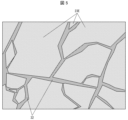
- FIG. 5 is an enlarged plan view of the light-emitting layer 23, particularly an enlarged plan view in the above-mentioned virtual plane.
- the recesses 32 may be formed randomly on the cathode 25 side of the light-emitting layer 23.
- the light-emitting layer 23 may have at least one closed region 23E surrounded by the recesses 32 in a plan view.
- At least one closed region 23E may include 10 5 to 10 8 quantum dots 30. Note that the closed region 23E in the present disclosure is preferably observed in a plan view in a virtual plane.
- the display device 1 may include a light-emitting element 2 for each subpixel, and the light-emitting layer 23 of each light-emitting element 2 may emit light of a color corresponding to each subpixel.
- the display device 1 may include, as the light-emitting elements 2, a red light-emitting element formed in the red subpixel, a green light-emitting element formed in the green subpixel, and a blue light-emitting element formed in the blue subpixel. In this case, the display device 1 can display full color by driving each light-emitting element 2 individually.
- Fig. 6 is a band diagram of the light-emitting layer 23 and the electron transport layer 24 among the layers of the light-emitting element 2.
- Fig. 6 shows the band gap between the quantum dots 30 and the inorganic matrix 31 of the light-emitting layer 23 and the electron transport layer 24, with the higher energy side of the electrons being the upper side as viewed in the plane of the paper.
- Fig. 6 also shows the band diagram in the portion where the light-emitting layer 23 and the electron transport layer 24 are in direct contact with each other.
- the quantum dots 30 are encapsulated in the inorganic matrix 31. Therefore, as shown in FIG. 6, the electron transport layer 24 contacts the inorganic matrix 31 of the light-emitting layer 23.
- the inorganic matrix 31 has a larger band gap than the quantum dots 30, the barrier to electron injection from the electron transport layer 24 to the inorganic matrix 31 is high. Therefore, in order to drive the light-emitting element 2 and inject electrons from the electron transport layer 24 into the quantum dots 30, it is necessary to cause the electrons to tunnel through the inorganic matrix 31.
- the band gap of the electron transport layer 24 in the vicinity of the interface with the inorganic matrix 31 is effectively curved downward. Therefore, as shown in FIG. 6, a quantum well 24W with a lower level than the surrounding area is formed on the upper end of the band gap of the electron transport layer 24 on the side of the light emitting layer 23.
- electrons ET injected from the cathode 25 into the electron transport layer 24 by driving the light-emitting element 2 may accumulate on the light-emitting layer 23 side of the electron transport layer 24, particularly in the quantum well 24W.
- the accumulated electrons ET may remain in the vicinity of the light-emitting layer 23 side of the electron transport layer 24 even when driving of the light-emitting element 2 is stopped.
- the accumulation of electrons ET may reduce the efficiency of electron injection into the quantum dots 30 in the light-emitting layer 23.
- the accumulated electrons ET may deteriorate the material of the light-emitting layer 23 or the layers surrounding the light-emitting layer 23 by generating Auger electrons, etc., and may shorten the life of the light-emitting element 2.
- the light-emitting layer 23 has a recess 32 on the cathode 25 side, and a part of the material constituting the electron transport layer 24 is located inside the recess 32. Therefore, in the light-emitting element 2 of this embodiment, even if the accumulation of electrons ET described above occurs, the electrons ET are quickly released to the cathode 25 side via the electron transport layer 24 inside the recess 32 by stopping the operation of the light-emitting element 2. Therefore, the light-emitting element 2 of this embodiment reduces the electrons ET that accumulate at the interface between the light-emitting layer 23 and the electron transport layer 24, improving the light-emitting efficiency or extending the life. A display device 1 including the light-emitting element 2 reduces power consumption or extends the life.
- the light-emitting layer 23 of the light-emitting element 2 according to this embodiment has an inorganic matrix 31 that fills the spaces between the multiple quantum dots 30. Therefore, in the light-emitting element 2, the inorganic matrix 31 protects the quantum dots 30 from foreign matter such as moisture, but the accumulation of electrons between the electron transport layer 24 and the inorganic matrix 31 may become significant.
- the light-emitting layer 23 of the light-emitting element 2 according to this embodiment has a recess 32 on the electron transport layer 24 side, so that the quantum dots 30 can be protected by the inorganic matrix 31 while more efficiently releasing electrons accumulated between the electron transport layer 24 and the inorganic matrix 31.
- the maximum width of the recess 32 in the in-plane direction of the light-emitting layer 23 is 1 ⁇ m, and the depth of the recess 32 in the film thickness direction of the light-emitting layer 23 is 20 nm.
- the cross-sectional area of the recess 32 in a cross section parallel to the film thickness direction of the light-emitting layer 23 is about 5000 nm2 .
- the electron transport layer 24 has ZnO nanoparticles with a median particle size of 6 nm.
- the material of the electron transport layer 24 fills the inside of the recess 32 and the number of ZnO nanoparticles located inside the recess 32 is minimal, the nanoparticles are considered to be aligned in a line from the bottom to the top of the recess 32.
- the number inside the recess 32 is approximately 3.3.
- the total cross-sectional area of the 3.3 nanoparticles having a particle size of 6 nm is about 93.3 nm2 . Therefore, when the number of nanoparticles located inside the recess 32 is a minimum, the ratio of the total cross-sectional area of the nanoparticles to the cross-sectional area of the recess 32 is about 1.9%.
- the material constituting the electron transport layer 24 is confirmed to be present in 1.9% or more of the portion that is located closer to the anode 21 than the imaginary plane VS and that contains a material different from the material constituting the light-emitting layer 23, then the material may be considered to fill the inside of the recess 32.
- the film thickness direction of the light-emitting layer 23 is the first direction D1, and the direction perpendicular to the first direction is the second direction D2.
- at least one quantum dot 30 may overlap the recess 32 in the second direction D2.
- the quantum dot 30 included in the closed region 23E is surrounded three-dimensionally by the recess 32, and is surrounded in particular in the second direction D2. This allows the light-emitting element 2 to more efficiently release electrons accumulated near the quantum dot 30 to the material located inside the recess 32, thereby more efficiently releasing the electrons.
- the light-emitting layer 23 may include an inorganic matrix 31 between the recesses 32 and the quantum dots 30. This reduces the quantum dots 30 exposed from the recesses 32 in the light-emitting element 2, improving the protective effect of the inorganic matrix 31 on the quantum dots 30.
- the layer thickness of the inorganic matrix 31 between the recesses 32 and the quantum dots 30 corresponds to the shortest distance L1 between the recesses 32 and the quantum dots 30. From the viewpoint of more reliably suppressing exposure of the quantum dots 30 from the recesses 32, the distance L1 may be 2 nm or more.
- the light-emitting layer 23 may include an inorganic matrix 31 between the end 32E of the recess 32 on the anode 21 side and the bottom surface 23U, which is the surface on the anode 21 side, and may further include quantum dots 30. This allows the light-emitting element 2 to suppress short-circuiting between the hole transport layer 22 and the electron transport layer 24 that occurs when the recess 32 comes into contact with the hole transport layer 22. From the viewpoint of more reliably suppressing short-circuiting between the hole transport layer 22 and the electron transport layer 24, the distance L2 between the end 32E and the bottom surface 23U may be 5 nm or more.
- the maximum width of the recess 32 in the second direction D2, or the width L3 at the end of the recess 32 on the electron transport layer 24 side corresponds to the width of the recess 32 in the above-mentioned imaginary plane VS, and may be 1 ⁇ m or more and 10 ⁇ m or less. This allows the light-emitting element 2 to release the above-mentioned accumulated electrons more efficiently, while ensuring an area where the light-emitting layer 23 and the electron transport layer 24 are in contact, and improving the efficiency of electron injection into the light-emitting layer 23.
- the maximum depth L4 of the recess 32 in the first direction corresponds to the distance between the imaginary plane VS and the end 32E.
- the maximum depth L4 may be less than the layer thickness of the light-emitting layer 23 in the first direction D1. This prevents short circuits between the hole transport layer 22 and the electron transport layer 24 in the light-emitting element 2, improving the luminous efficiency of the light-emitting layer 23.
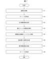
- Fig. 7 is a flow chart showing the method for manufacturing the display device 1 according to this embodiment.
- the substrate 3 is prepared (step S3).
- the substrate 3 may be manufactured, for example, by forming a plurality of the pixel circuits PC described above on a glass substrate.
- the light-emitting element 2 is formed on the substrate 3.
- the anode 21 is formed on the substrate 3 by any of the methods described above (step S2).
- the anode 21 may be formed in an island shape for each pixel circuit PC.
- the hole transport layer 22 is formed by any of the methods described above (step S3).
- the hole transport layer 22 may be formed in common for the multiple anodes 21, or may be formed in an island shape for each anode 21.
- the material of the hole transport layer 22 may differ depending on the emission color of the sub-pixel.
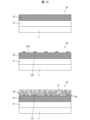
- FIG. 8 and FIG. 9 are process cross-sectional views showing the manufacturing method of the display device 1, and in particular show the process of forming the light-emitting layer 23 and the electron transport layer 24 in detail. Note that each process cross-sectional view in this disclosure, including FIG. 8 and FIG. 9, shows a cross section corresponding to the cross section of the display device 1 shown in FIG. 1.
- a quantum dot dispersion liquid 23A which is a dispersion liquid in which quantum dots 30 and precursors 31A of the inorganic matrix 31 are dispersed in a liquid, is applied (step S4).
- the laminate from the substrate 3 to the hole transport layer 22 is regarded as a substrate, and the quantum dot dispersion liquid 23A is applied to the substrate by various application methods such as spin coating.
- a thin film of the inorganic matrix 31 may be formed on the hole transport layer 22 prior to application of the quantum dot dispersion liquid 23A.
- the quantum dot dispersion liquid 23A may be prepared before step S4.
- the quantum dot dispersion liquid 23A may be prepared, for example, by stirring a dispersion liquid of quantum dots 30 coordinated with organic ligands and a dispersion liquid of precursor 31A to obtain a dispersion liquid of quantum dots 30 coordinated with precursor 31A.
- the precursor 31A may contain, for example, 3-(mercaptopropyl)trimethoxysilane (MPS) or tetramethyl orthosilicate (TMOS) as a precursor of silicon oxide.
- MPS 3-(mercaptopropyl)trimethoxysilane
- TMOS tetramethyl orthosilicate
- the precursor 31A is transformed into an inorganic matrix 31 by, for example, heating the applied quantum dot dispersion liquid 23A (step S5).
- a light-emitting material layer 23B is formed that includes a plurality of quantum dots 30 and an inorganic matrix 31 that fills the spaces between the plurality of quantum dots 30.
- FIG. 10 is a schematic diagram of a cross section of the hole transport layer 22 and the light-emitting material layer 23B or the light-emitting layer 23 to illustrate the method of forming recesses 32.
- step S6 the light-emitting material layer 23B is formed on the hole-transport layer 22.
- the laminate on the substrate 3 including the hole-transport layer 22 and the light-emitting material layer 23B is heated and then rapidly cooled.
- the laminate may be heated from room temperature to 130°C, held at the heating temperature for 5 minutes, and then cooled to room temperature in about 1 minute.
- the above-mentioned heating causes the hole transport layer 22 and the light emitting material layer 23B to thermally expand
- the above-mentioned rapid cooling causes the hole transport layer 22 and the light emitting material layer 23B to attempt to restore their original shapes. Therefore, the above-mentioned rapid cooling causes stress F1 in the hole transport layer 22 and stress F2 in the light emitting material layer 23B, as shown in step S6-2 of FIG. 10. Stresses F1 and F2 occur in the directions that cause the hole transport layer 22 and the light emitting material layer 23B to contract, respectively.
- the inorganic matrix 31 containing silicon oxide etc. has a lower rate of thermal expansion than the material contained in the hole transport layer 22. Therefore, stress F2 tends to be smaller than stress F1. Therefore, the above-mentioned rapid cooling generates a difference in the stresses generated in the hole transport layer 22 and the light emitting material layer 23B, and in particular, compressive stress occurs near the interface between the hole transport layer 22 and the light emitting material layer 23B, and tensile stress occurs near the upper surface of the light emitting material layer 23B.
- the above heating step may be performed by rapid heating from room temperature to 130°C in about one minute, for example.
- step S6-3 of FIG. 10 part of the inorganic matrix 31 will break from the top surface side that is not joined to the hole transport layer 22.
- a recess 32 is formed in the light-emitting material layer 23B, recessed in the direction from the surface on the side opposite the hole transport layer 22 toward the hole transport layer 22, and a light-emitting layer 23 having the recess 32 is formed.
- step S6 deterioration of the materials that make up the light-emitting layer 23, such as the quantum dots 30, can be reduced compared to when the recess 32 is directly formed by etching the light-emitting material layer 23B, for example.
- the modification of the precursor 31A to the inorganic matrix 31 and the formation of the recesses 32 may be performed in the same process.
- the applied quantum dot dispersion liquid 23A may be rapidly heated and then rapidly cooled, thereby forming the recesses 32 while modifying the precursor 31A to the inorganic matrix 31.
- the electron transport layer 24 is formed (step S7).
- the electron transport layer 24 is formed by forming a layer of the material constituting the electron transport layer 24 on the upper surface of the light-emitting layer 23 on the side of the recesses 32 by a coating method, a vapor deposition method, or the like.
- the material constituting the electron transport layer 24 is also formed inside the recesses 32.
- the formation of the electron transport layer 24 and the formation of the material constituting the electron transport layer 24 inside the recesses 32 can be performed in the same process.
- the electron transport layer 24 may be formed in common to the multiple anodes 21, as with the hole transport layer 22, or may be formed for each anode 21.
- a cathode 25 is formed on the electron transport layer 24 by the various methods described above (step S8).
- the cathode 25 may be formed in common for multiple anodes 21. In this manner, a display device 1 having light-emitting elements 2 on a substrate 3 is manufactured.
- ⁇ Evaluation of Light-emitting Device> In order to verify the characteristics of the light-emitting device 2 according to this embodiment, light-emitting devices according to an example, a comparative example 1, and a comparative example 2 were manufactured.
- the light-emitting device according to the example has the same configuration as the light-emitting device according to this embodiment.
- the light-emitting device according to the comparative example 1 has the same configuration as the light-emitting device according to this embodiment, except that the light-emitting layer 23 does not have a recess 32.
- the light-emitting device according to the comparative example 2 has the same configuration as the light-emitting device according to this embodiment, except that the light-emitting layer 23 does not have an inorganic matrix 31, and an organic ligand is coordinated to each quantum dot 30.
- ITO In the manufacturing method of the light-emitting element according to the embodiment, first, ITO was formed on a substrate by sputtering to form an anode 21. Next, a hole injection layer containing NiO was formed on the anode 21 by spin coating and baking. Next, an organic SAM (Self Assemble Monolayer) film was formed on the hole injection layer by spin coating and baking. Next, an organic hole transport material layer was formed on the SAM film by spin coating and baking. This formed a hole transport layer 22 containing a SAM film and a hole transport material layer.
- ITO In the manufacturing method of the light-emitting element according to the embodiment, first, ITO was formed on a substrate by sputtering to form an anode 21. Next, a hole injection layer containing NiO was formed on the anode 21 by spin coating and baking. Next, an organic SAM (Self Assemble Monolayer) film was formed on the hole injection layer by spin coating and baking. Next, an organic hole transport material layer was formed on the
- a thin film of ZnS was formed on the hole transport layer 22, and then a quantum dot dispersion liquid 23A containing quantum dots 30 coordinated with MPS, which is a precursor 31A, was applied on the ZnS thin film and baked.
- the laminate including the light-emitting material layer 23B was rapidly heated and then rapidly cooled by the method described above, to form recesses 32 in the light-emitting material layer 23B, thereby forming the light-emitting layer 23.
- a dispersion liquid in which nanoparticles of the electron transport material are dispersed was applied onto the light-emitting layer 23 by a spin coating method, and the resulting mixture was baked, to form the electron transport layer 24.
- a cathode 25 was formed on the electron transport layer 24 by a vacuum deposition method, thereby producing the light-emitting device according to the example.
- the light-emitting element according to Comparative Example 1 was manufactured by the same method as the light-emitting element according to the above-mentioned Example, except that the light-emitting material layer 23B was not rapidly heated or cooled. Therefore, in the method of manufacturing the light-emitting element according to the Comparative Example, the light-emitting material layer 23B without the recess 32 became the light-emitting layer as it is.
- the light-emitting element according to Comparative Example 2 was manufactured by the same method as the light-emitting element according to the above-mentioned Example, except that the light-emitting layer 23 was formed by applying and baking a dispersion of quantum dots 30 coordinated with organic ligands.
- the light-emitting element according to the Example has improved reliability compared to the light-emitting elements according to Comparative Examples 1 and 2.
- the light-emitting element according to the Example exhibits a reduction in luminance, which is believed to be due to the accumulation of electrons near the interface between the light-emitting layer 23 and the electron transport layer 24, which is resolved more quickly when the operation of the light-emitting element is stopped, compared to the light-emitting elements according to each of the Comparative Examples.
- the light-emitting element according to the Example has a lower concentration of organic ligands in the light-emitting layer 23 compared to the light-emitting element according to Comparative Example 2.
- the light-emitting element according to the Example has a light-emitting layer 23 with reduced organic ligands that strongly capture electrons, and therefore electrons accumulated near the interface between the light-emitting layer 23 and the electron transport layer 24 are released more quickly.
- the number of quantum dots 30 in the closed region 23E surrounded by the recess 32 was considered as follows.
- the light-emitting layer 23 of the light-emitting element according to the embodiment was observed in a virtual plane VS, five closed regions 23E including closed region 1 to closed region 5 were identified, and the area of each closed region 23E was calculated.
- the area of each closed region 23E was calculated by obtaining an image of the cross section of the observed light-emitting layer 23, identifying the boundary of the closed region 23E from the brightness and darkness of the image, and measuring the number of pixels contained in the closed region 23E.
- the boundary of the closed region 23E may also be identified by observing a cross section parallel to the film thickness direction of the light-emitting layer 23.
- the number of quantum dots 30 contained in each closed region 23E is calculated by dividing the area of the closed region 23E by the cross-sectional area of the cross-section passing through the center of the quantum dot 30.
- any cross-section of the light-emitting layer 23 is observed by a TEM (transmission electron microscope) at a magnification of 200,000 times or more, the average particle diameter D of at least 500 quantum dots 30 is calculated, and ⁇ (D/2) 2 is set as the cross-sectional area of the quantum dots 30.
- the maximum width of the observed quantum dots 30 is set as the particle diameter of the quantum dots 30.
- the “Closed region area” column indicates the area of each closed region 23E.
- the “QD emission color” column indicates the emission color of the quantum dots 30 contained in each closed region 23E.
- the quantum dots 30 whose emission color is “red” have an average particle size D of 10 nm and a cross-sectional area of 78.5 nm2 .
- the quantum dots 30 whose emission color is “green” have an average particle size D of 5 nm and a cross-sectional area of 19.6 nm2 .
- the quantum dots 30 whose emission color is “blue” have an average particle size D of 6 nm and a cross-sectional area of 28.3 nm2 .
- the "QD number” column indicates the number of quantum dots 30 contained in each closed region 23E when the emission color of the quantum dots 30 is the color indicated by "QD emission color”.
- the number of quantum dots 30 contained in each of the closed regions 1 to 5 is 10 5 or more and 10 9 or less. This corresponds to the number of quantum dots 30 surrounded by the recess 32 being 10 5 or more and 10 9 or less. Since the number of quantum dots 30 contained in the closed region 23E is 10 5 or more, the light-emitting element 2 can more efficiently emit light in the closed region 23E.
- the outer peripheral area of a group of quantum dots 30 surrounded by the recess 32 is proportional to the 1/3 power of the number of the group of quantum dots 30. Therefore, the outer peripheral area per one of the group of quantum dots 30 is proportional to the ⁇ 1/3 power of the number of the group of quantum dots 30.
- step S6 by adjusting the heating and cooling speed in step S6, the difference in stress between the hole transport layer 22 and the light emitting material layer 23B can be adjusted, and thus the number or spacing of the recesses 32 formed can be adjusted.
- the size of each closed region 23E can be adjusted, and in combination with adjusting the particle size of the quantum dots 30 contained in the light emitting layer 23, the number of quantum dots 30 contained in each closed region 23E can be adjusted.
- FIG. 11 is a schematic side cross-sectional view of a display device 4 according to another embodiment of the present disclosure.
- the display device 4 according to this embodiment includes a light-emitting element 5 instead of the light-emitting element 2.
- the light-emitting element 5 includes a light-emitting layer 26 instead of the light-emitting layer 23.
- the light-emitting layer 26 has a recess 33 instead of the recess 32.
- the recess 33 is located on the surface on the anode 21 side, and is recessed towards the cathode 25 side.
- a part of the material constituting the hole transport layer 22 is located inside the recess 33.
- the display device 4 has the same configuration as the display device 1 according to the previous embodiment.
- the light-emitting element 5 has, on an anode 21 as a second electrode, a hole transport layer 22 as a first charge transport layer, a light-emitting layer 26 as a first light-emitting layer, an electron transport layer 24, and a cathode 25 as a first electrode, in this order from the substrate 3 side.
- the difference in band gap between the hole transport layer 22, the quantum dots 30, and the inorganic matrix 31 may hinder hole injection from the hole transport layer 22 to the quantum dots 30. For this reason, in the light-emitting element 5, holes may accumulate near the interface between the hole transport layer 22 and the light-emitting layer 26.
- the light-emitting layer 26 of the light-emitting element 5 has a recess 33 as a first recess on the surface on the anode 21 side, in which part of the material constituting the hole transport layer 22 is located. Therefore, in the light-emitting element 5 according to this embodiment, even if the accumulation of holes described above occurs, the holes are quickly released to the anode 21 side via the hole transport layer 22 inside the recess 33 by stopping the driving of the light-emitting element 5.
- the carrier balance in the light-emitting layer may result in an excess of holes.
- the accumulation of holes on the anode side of the light-emitting layer may become significant.
- the light-emitting element 5 of this embodiment efficiently reduces the excess of holes in the light-emitting layer 26 or the excess of holes at the interface between the hole transport layer 22 and the light-emitting layer 26 through the recess 33. Therefore, the light-emitting element 5 can efficiently achieve an improvement in light-emitting efficiency or an extension of the life span.
- FIG. 12 is a flowchart showing a method for manufacturing a display device 4 according to this embodiment. Note that, for each step shown in the flowchart of this disclosure, steps that can be executed with the same content are given the same reference numbers.
- the display device 4 according to this embodiment may be manufactured in the same manner as the manufacturing method of the display device 1 according to the previous embodiment, except that step S9 is performed after step S3 instead of step S6. Specifically, in the manufacturing method of the display device 4 according to this embodiment, after step S3, a convex portion or a concave portion serving as a fifth concave portion is formed in the hole transport layer 22 (step S9), and step S7 is performed after step S5.
- FIG. 13 is a cross-sectional view showing the steps in the manufacturing method of the display device 4, and in particular shows in detail the steps of forming convex and concave portions in the hole transport layer 22.
- step S3 of FIG. 8 When the formation of the hole transport layer 22 is completed, as shown in step S3 of FIG. 8, the anode 21 and the hole transport layer 22 are formed in this order on the substrate 3.
- step S9 of FIG. 13 in step S3, a convex portion 22P that protrudes upward, or a concave portion 22C as a fifth concave portion recessed toward the anode 21, is formed on the upper surface side of the hole transport layer 22.
- step S9 following the deposition of the hole transport layer 22, the material of the hole transport layer 22 may be imprinted onto the hole transport layer 22 to form a convex portion 22P in the hole transport layer 22.
- step S9 following the deposition of the hole transport layer 22, a portion of the hole transport layer 22 may be etched to form a concave portion 22C in the hole transport layer 22. Note that in step S9, only one of the formation of the convex portion 22P and the formation of the concave portion 22C may be performed, or both may be performed.
- steps S4 and S5 are performed to form the light-emitting layer 26 on the upper surface of the hole transport layer 22 on which the convex portion 22P or the concave portion 22C is formed.
- the light-emitting material layer formed in step S5 becomes the light-emitting layer 26 as it is.
- the shape of the lower surface of the light-emitting layer 26 reflects the shape of the upper surface of the hole transport layer 22 having the convex portion 22P or the concave portion 22C. Therefore, by performing the formation process of the light-emitting layer 26 following step S9, a concave portion 33 is formed on the surface of the light-emitting layer 26 on the anode 21 side.
- the shape of the concave portion 33 can be designed by designing the shape of the convex portion 22P or the concave portion 22C formed in step S9, the above manufacturing method makes it easier to design the shape of the concave portion 33 and improves the accuracy of the shape of the concave portion 33.
- FIG. 14 is a schematic side cross-sectional view of a display device 6 according to another embodiment of the present disclosure.
- the display device 6 according to this embodiment includes a light-emitting element 7 instead of the light-emitting element 2.
- the light-emitting element 7 includes, in this order from the substrate 3 side, a cathode 25 as a first electrode, an electron transport layer 24, a light-emitting layer 23 as a first light-emitting layer, a hole transport layer 22 as a first charge transport layer, and an anode 21 as a second electrode.
- a part of the material constituting the hole transport layer 22 is located inside the recess 32 of the light-emitting layer 23 according to this embodiment.
- each layer of the light-emitting element 7 may have the same configuration as each layer of the light-emitting element 2 except for the stacking order, and in particular may be made of the same material as each layer of the light-emitting element 2.
- the cathode 25 according to this embodiment may be formed for each pixel circuit PC, and the anode 21 may be formed in common to the multiple cathodes 25.
- the light-emitting element 7 for the same reason as described above, the holes accumulated near the interface between the light-emitting layer 23 and the hole transport layer 22 are quickly released to the anode 21 side through the hole transport layer 22 inside the recess 33. Therefore, the light-emitting element 7 can efficiently achieve improved light-emitting efficiency or longer life.
- the display device 6 may be manufactured by performing steps S1, S8, S7, S4, S5, S6, S3, and S2 in this order among the above-mentioned steps.
- step S3 a part of the material of the hole transport layer 22 is formed inside the recess 32 of the light-emitting layer 23 formed in step S6.
- FIG. 15 is a schematic side cross-sectional view of a display device 8 according to another embodiment of the present disclosure.
- the display device 8 according to this embodiment includes a light-emitting element 9 instead of the light-emitting element 7.
- the light-emitting element 9 includes a light-emitting layer 26 instead of the light-emitting layer 23. Therefore, a part of the material constituting the electron transport layer 24 is located inside the recess 33 of the light-emitting layer 26 according to this embodiment.
- the display device 8 has the same configuration as the display device 6 according to the previous embodiment.
- the light-emitting element 9 has, on a cathode 25 as a second electrode, an electron transport layer 24 as a first charge transport layer, a light-emitting layer 23 as a first light-emitting layer, a hole transport layer 22, and an anode 21 as a first electrode, in this order from the substrate 3 side.
- the light-emitting element 9 for the same reason as described above, electrons accumulated near the interface between the light-emitting layer 26 and the electron transport layer 24 are quickly released to the cathode 25 side through the electron transport layer 24 inside the recess 33. Therefore, the light-emitting element 9 can efficiently achieve improved light-emitting efficiency or longer life.
- the display device 6 may be manufactured by performing steps S1, S8, S7, S9, S4, S5, S3, and S2 in this order among the above-mentioned steps.
- step S9 convex portions or concave portions are formed in the electron transport layer 24. Therefore, in the subsequent process of forming the light-emitting layer 26, the light-emitting layer 26 reflects the shape of the convex portions or concave portions of the electron transport layer 24, and therefore concave portions 33 are formed in the light-emitting layer 26.
- ⁇ Second Recess> 16 is a schematic side cross-sectional view of a display device 10 according to another embodiment of the present disclosure.
- the display device 10 according to this embodiment includes a light-emitting element 11 instead of the light-emitting element 2.
- the light-emitting element 11 includes a light-emitting layer 27 instead of the light-emitting layer 23.
- the light-emitting layer 27 has a recess 33 as a second recess in addition to a recess 32 as a first recess.
- the light-emitting layer 27 has both a recess 32 located on the surface on the cathode 25 side and recessed toward the anode 21 side, and a recess 33 located on the surface on the anode 21 side and recessed toward the cathode 25 side. Furthermore, part of the material constituting the electron transport layer 24 as the first charge transport layer is located inside the recess 32, and part of the material constituting the hole transport layer 22 as the second charge transport layer is located inside the recess 33.
- the light-emitting element 11 In the light-emitting element 11 according to this embodiment, electrons accumulated near the interface between the light-emitting layer 27 and the electron transport layer 24 are quickly released to the cathode 25 side through the electron transport layer 24 inside the recess 32. Furthermore, in the light-emitting element 11 according to this embodiment, holes accumulated near the interface between the light-emitting layer 27 and the hole transport layer 22 are quickly released to the anode 21 side through the hole transport layer 22 inside the recess 33. In other words, the light-emitting element 11 quickly releases both the electrons and holes accumulated near the light-emitting layer 27. Therefore, the light-emitting element 11 can more efficiently achieve improved luminous efficiency or longer life.
- the inside of the recess 32 may be filled with a part of the material constituting the electron transport layer 24, and the inside of the recess 33 may be filled with a part of the material constituting the hole transport layer 22. This allows the light-emitting element 11 to more quickly release both the electrons and holes accumulated near the light-emitting layer 27, and more efficiently achieve improved light-emitting efficiency or longer life.
- the display device 10 may be manufactured by the same method, except that step S9 is further performed following step S3.
- the light-emitting material layer formed in steps S4 and S5 reflects the shape of the convex portion 22P or the concave portion 22C of the hole transport layer 22 formed in step S9, and a concave portion 33 is formed on the surface of the light-emitting material layer on the anode 21 side.
- a concave portion 32 is formed on the upper surface of the light-emitting material layer, and a light-emitting layer 27 is formed.
- FIG. 17 is a schematic side cross-sectional view of a display device 12 according to another embodiment of the present disclosure.
- the display device 12 according to this embodiment includes a light-emitting element 13 instead of the light-emitting element 2.
- the light-emitting element 13 includes a first portion 14, a charge generating layer 15, and a second portion 16 laminated in this order from the substrate 3 side.
- the first section 14 comprises, in order from the substrate 3 side, an anode 21 as a first electrode, a hole transport layer 22, a light-emitting layer 23 as a first light-emitting layer, and an electron transport layer 24 as a first charge transport layer.
- the light-emitting layer 23 of the first section 14 has a recess 32 recessed toward the anode 21 on the surface on the side of the cathode 25 of the second section 16 described below, and a part of the material of the electron transport layer 24 is located inside the recess 32. Therefore, the first section 14 may have a laminated structure in which only the cathode 25 is removed from the light-emitting element 2 described above.
- the second section 16 comprises, in order from the charge generation layer 15 side, a hole transport layer 22, a light-emitting layer 23 as a second light-emitting layer, an electron transport layer 24 as a third charge transport layer, and a cathode 25 as a second electrode.
- the light-emitting layer 23 of the second section 16 has a recess 32 as a third recess recessed toward the anode 21 of the first section 14 on the surface on the cathode 25 side, and a part of the material of the electron transport layer 24 is located inside the recess 32. Therefore, the second section 16 may have a laminated structure in which only the anode 21 is removed from the light-emitting element 2 described above.
- the charge generation layer 15 is a layer that generates charges in response to the potential difference between the anode 21 of the first section 14 and the cathode 25 of the second section 16, in other words, in response to driving of the light-emitting element 13. In particular, when the light-emitting element 13 is driven, the charge generation layer 15 injects electrons into the electron transport layer 24 of the first section 14 and injects holes into the hole transport layer 22 of the second section 16.
- the charge generation layer 15 may include, for example, an electron generation layer located on the first section 14 side and including an n-type semiconductor, and a hole generation layer located on the second section 16 side and including a p-type semiconductor.
- the charge generation layer 15 can be formed by a vacuum deposition method, a sputtering method, a coating formation method using a colloidal solution, or the like.
- the light-emitting layer 23 in the first section 14 and the light-emitting layer 23 in the second section 16 may emit light of the same color or different colors.
- the display device 12 may be provided with a color filter corresponding to the emission color of each sub-pixel on the side of the cathode 25 of the light-emitting element 13.
- the light-emitting element 13 can achieve improved luminous efficiency or longer life in both the first portion 14 and the second portion 16 while causing both the light-emitting layer 23 in the first portion 14 and the light-emitting layer 23 in the second portion 16 to emit light.
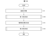
- FIG. 18 is a flowchart showing a method for manufacturing the display device 12 according to this embodiment.
- step S1 is first performed, and then the first portion 14 is formed on the substrate 3 (step S10).
- the first portion 14 may be formed by sequentially performing steps S2 to S7 of the method for manufacturing the display device 1.
- Step S11 a charge generating layer 15 is formed on the electron transport layer 24 of the first portion 14 (step S11).
- Step S11 may be performed, for example, by forming an electron generating layer and a hole generating layer in sequence by the method described above.
- the second portion 16 is formed on the charge generating layer 15 (step S12).
- the second portion 16 may be formed by sequentially performing steps S3 to S8 of the manufacturing method of the display device 1. In this manner, the display device 12 according to this embodiment is manufactured.
- the display device 12 includes a light-emitting element 13 in which a first section 14 including a first light-emitting layer and a second section 16 including a second light-emitting layer are stacked with a charge generation layer 15 interposed therebetween, but is not limited to this.
- the light-emitting element 13 may further include a charge generation layer, a hole transport layer, a third light-emitting layer, and an electron transport layer, in this order from the anode 21 side, between the electron transport layer 24 and the charge generation layer 15 of the first section 14, or between the electron transport layer 24 and the cathode 25 of the second section.
- the positions of the first light-emitting layer, the second light-emitting layer, and the third light-emitting layer may be interchanged.
- the first light-emitting layer, the second light-emitting layer, and the third light-emitting layer may emit red light, green light, and blue light, respectively, and may be formed in common across multiple sub-pixels.
- the display device 12 may be provided with a red color filter, a green color filter, and a blue color filter corresponding to each sub-pixel on the cathode 25 side of the light-emitting element 11. This allows the display device 12 to display in full color without requiring patterning of each light-emitting layer in the manufacturing process of the light-emitting element 11.
- FIG. 7 is a schematic side cross-sectional view of a display device 17 according to another embodiment of the present disclosure.
- the display device 17 according to this embodiment includes a light-emitting element 18 instead of the light-emitting element 13.
- the light-emitting element 18 includes a first portion 19 instead of the first portion 14 and a second portion 20 instead of the second portion 16.
- the first section 19 has a light-emitting layer 27 instead of the light-emitting layer 23. Therefore, the first section 19 has an anode 21 as a first electrode, a hole transport layer 22 as a second charge transport layer, a light-emitting layer 27 as a first light-emitting layer, and an electron transport layer 24 as a first charge transport layer.
- the light-emitting layer 27 of the first section 19 has a recess 33 as a second recess recessed toward the cathode 25 of the second section 20 described later on the surface on the anode 21 side, and a part of the material of the hole transport layer 22 is located inside the recess 33. Therefore, the first section 19 may have a laminated structure in which only the cathode 25 is removed from the light-emitting element 11 described above.
- the second part 20 has a light-emitting layer 27 instead of the light-emitting layer 23. Therefore, the second part 20 has a hole transport layer 22 as a fourth charge transport layer, a light-emitting layer 27 as a second light-emitting layer, an electron transport layer 24 as a third charge transport layer, and a cathode 25 as a second electrode.
- the light-emitting layer 27 of the second part 20 has a recess 33 as a fourth recess recessed toward the cathode 25 on the surface on the anode 21 side of the first part 19, and a part of the material of the hole transport layer 22 is located inside the recess 33. Therefore, the second part 20 may have a laminated structure in which only the anode 21 is removed from the above-mentioned light-emitting element 11.
- the display device 17 according to this embodiment has the same configuration as the display device 12 according to the previous embodiment. Therefore, when the light-emitting element 18 is driven, holes from the anode 21 and electrons from the charge generation layer 15 are injected into the light-emitting layer 27 of the first portion 19, and holes from the charge generation layer 15 and electrons from the cathode 25 are injected into the light-emitting layer 27 of the second portion 20. Therefore, when the light-emitting element 18 is driven, the display device 17 extracts light from both the light-emitting layer 27 of the first portion 19 and the light-emitting layer 27 of the second portion 20.
- the electrons and holes accumulated near the light-emitting layer 27 are quickly released via the charge transport material in the recesses 32 and 33, respectively. Therefore, the light-emitting element 18 can more efficiently achieve improved luminous efficiency or longer life in both the first section 19 and the second section 20 while causing both the light-emitting layer 27 in the first section 19 and the light-emitting layer 27 in the second section 20 to emit light.
- the display device 17 according to this embodiment may be manufactured by a method in which some steps of the manufacturing method of the display device 12 according to the previous embodiment are modified.
- the display device 17 may be manufactured by a method in which step S9, which follows step S3, is added to each of steps S10 and S12 of the manufacturing method of the display device 12.
Landscapes
- Physics & Mathematics (AREA)
- Optics & Photonics (AREA)
- Engineering & Computer Science (AREA)
- Manufacturing & Machinery (AREA)
- Chemical & Material Sciences (AREA)
- Crystallography & Structural Chemistry (AREA)
- Inorganic Chemistry (AREA)
- Nanotechnology (AREA)
- Electroluminescent Light Sources (AREA)
Abstract
発光素子(2)は、第1電極(21)と、第2電極(25)と、第1発光層(23)と、第1電荷輸送層(24)と、を備える。発光層は、第1電極と第2電極との間に位置するとともに、第2電極の側の表面に第1電極の側に向かって窪む第1凹部(32)を有する。第1電荷輸送層は第1発光層の第2電極の側に接し、第1電荷輸送層を構成する材料の一部は第1凹部の内側に位置する。
Description
本開示は、発光素子、当該発光素子を備えた表示装置、および当該発光素子の製造方法に関する。
特許文献1には、半導体または金属原子を含むマトリクス中に量子ドット(半導体ナノ粒子)を有する量子ドット構造体が開示されている。マトリクス中に量子ドットを有する構造体は、マトリクスにより量子ドットを保護して量子ドットの信頼性を向上させる。
特許文献1に記載されているようなマトリクス中に量子ドットを含む構造体は、発光素子の発光層としての利用例が考えられる。しかしながら、当該発光素子においては各電極からの電荷の量子ドットへの注入がマトリクスにより阻害され発光層と電荷輸送層との界面に電荷が蓄積する問題が生じる場合があり、このような電荷の蓄積は、発光素子の発光効率の低下、または発光層および発光層の周囲の層の劣化に伴う発光素子の寿命の短期化を引き起こす場合がある。
本開示の一態様に係る発光素子は、第1電極と、前記第1電極に対向する第2電極と、前記第1電極と前記第2電極との間に位置するとともに、前記第2電極の側の表面に前記第1電極の側に向かって窪む第1凹部を有する第1発光層と、前記第1発光層の前記第2電極の側に接する第1電荷輸送層と、を備え、前記第1電荷輸送層を構成する材料の一部が前記第1凹部の内側に位置する。
本開示の一態様に係る発光素子の製造方法は、第1電極の形成と、前記第1電極に対向する第2電極の形成と、前記第1電極と前記第2電極との間に位置するとともに、前記第2電極の側の表面に前記第1電極の側に向かって窪む第1凹部を有する第1発光層の形成と、前記第1発光層の前記第2電極の側に接する第1電荷輸送層の形成と、を含み、前記第1電荷輸送層の形成においては、前記第1電荷輸送層を構成する材料の一部が前記第1凹部の内側に位置する。
本開示の一態様に係る構成によれば、発光層と電荷輸送層との界面に蓄積する電荷を低減し、発光効率が向上した、または寿命が長期化した発光素子を実現する。
〔実施形態1〕
<表示装置:概要>
以下、本開示の実施形態について図面を参照しつつ説明する。なお、各図面において、同様の構成については同一の符号を付してその説明を省略する。
<表示装置:概要>
以下、本開示の実施形態について図面を参照しつつ説明する。なお、各図面において、同様の構成については同一の符号を付してその説明を省略する。
図2は本実施形態に係る表示装置1の概略図である。表示装置1は、例えば、テレビまたはスマートフォン等のディスプレイに用いることのできる装置である。表示装置1は、複数のサブ画素Xを含む表示部DAと、複数のサブ画素Xを駆動するドライバ回路DRとを備える。複数のサブ画素Xの少なくとも1つは、発光素子2と当該発光素子2を駆動する画素回路PCとを備える。表示装置1は、ドライバ回路DRおよび画素回路PCを介して表示部DAに形成された複数の発光素子2のそれぞれからの発光を制御することにより、表示部DAにおいて表示を行う。
表示装置1の表示部DAにおける構造、特に発光素子2の構造について、図1を参照してより詳細に説明する。図1は本開示の実施形態に係る表示装置1の概略側断面図であり、特に、表示装置1の表示面と垂直な断面、かつ、発光素子2を通る断面について示す。なお、本開示における表示装置の各工程断面図は、図1に示す表示装置1の断面に対応する断面を示す。
図1に示すように、本実施形態に係る表示装置1は、表示部DAにおいて、上述した複数の発光素子2と基板3とを備え、特に基板3上に複数の発光素子2を備える。表示装置1は、例えば図示しないTFT(Thin Film Transistor)が画素回路PCとして形成された基板3上に、発光素子2の各層が積層された構造を備える。なお、本明細書においては、表示装置1の発光素子2から基板3への方向を「下方向」、当該下方向と反対方向を「上方向」として記載する。
発光素子2は、第1電極としてのアノード21上に、正孔輸送層22と、第1発光層としての発光層23と、第1電荷輸送層としての電子輸送層24と、第2電極としてのカソード25とを、基板3の側からこの順に備える。発光素子2のアノード21は、基板3のTFTと電気的に接続されている。
<発光素子の概要>
以下、発光素子2の各層の構成について、より詳細に説明する。
以下、発光素子2の各層の構成について、より詳細に説明する。
アノード21およびカソード25は導電性材料を含み、それぞれ、正孔輸送層22および電子輸送層24と電気的に接続されている。
アノード21とカソード25との少なくとも何れか一方は、可視光を透過する透明電極である。透明電極としては、例えば、ITO(酸化インジウムスズ)、IZO(酸化インジウム亜鉛)、ZnO、AZO(アルミニウムドープ酸化亜鉛、ZAOとも称される)、BZO(ボロンドープ酸化亜鉛)またはFTO(フッ素ドープ酸化スズ)等が用いられる。透明電極は、スパッタ法等によって成膜されてもよい。また、アノード21またはカソード25のいずれか一方は金属材料を含んでいてもよく、金属材料としては、可視光の反射率の高いAl、Cu、Au、AgまたはMgの単独またはこれらの合金が好ましい。
正孔輸送層22は、アノード21からの正孔を発光層23へと輸送する、正孔輸送材料を含む層である。正孔輸送層22の材料には、量子ドットを含む発光素子等において、従来から採用されている、有機または無機の材料を使用することができる。例えば、正孔輸送層22は正孔輸送材料として、ポリビニルカルバゾール(PVK)、および[N,N’-ビス(4-ブチルフェニル)-N,N’-ビス(フェニル)-ベンジジン](TPD)のうち少なくとも1種を含んでもよい。また、正孔輸送層22の有機材料としては、4,4’-ビス(カルバゾール-9-イル)ビフェニル(CBP)、ポリフェニレンビニレン(PPV)、ポリ(3,4-エチレンジオキシチオフェン)(PEDOT)とポリスチレンスルホン酸(PSS)との複合物(PEDOT-PSS)、ポリ[(9,9-ジオクチルフルオレニル-2,7-ジイル)-co-(4,4’-(N-4-sec-ブチルフェニル)ジフェニルアミン)])(TFB)等の導電性化合物が使用できる。正孔輸送層22の無機材料としては、モリブデン酸化物、NiO、Cr2O3、MgO、MgZnO、LaNiO3、MoO3、またはWO3等の金属酸化物を使用できる。特に、正孔輸送層22の材料としては、電子親和力およびイオン化ポテンシャルが大きい材料が好適である。
電子輸送層24は、カソード25からの電子を発光層23へと輸送する、電子輸送材料を含む層である。電子輸送層24の材料には、量子ドットを含む発光素子等において、従来から採用されている、有機または無機の材料を使用することができる。例えば、電子輸送層24は電子輸送材料として、酸化亜鉛(ZnO)、酸化マグネシウム亜鉛(ZnMgO)、酸化チタン(TiO)、および酸化タングステン(WO3)のうち少なくとも1種を含んでもよく、また、これらの無機材料のナノ粒子である無機ナノ粒子材料を含んでもよい。あるいは、電子輸送層24は電子輸送材料として、トリス(8-キノリノール)アルミニウム錯体(Alq3)、バソクプロイン(BCP)または(2-(4-ビフェニリル)-5-(4-tert-ブチルフェニル)-1,3,4-オキサジアゾール)(t-Bu-PBD)等の、有機材料を含んでもよい。なお、電子輸送層24の無機材料としては、ZnO、ZAO、ITO、InGaZnOまたはエレクトライド等の金属酸化物を使用してもよい。特に、電子輸送層24の材料としては、電子親和力が小さい材料が好適である。
本実施形態において、正孔輸送層22および電子輸送層24は、上述した材料を使用した、真空蒸着法、スパッタ法、またはコロイド溶液を用いた塗布形成法等により形成できる。また、発光素子2は、アノード21と正孔輸送層22との間に、正孔注入層を備えていてもよく、カソード25と電子輸送層24との間に、電子注入層を備えていてもよい。さらに、発光素子2は、正孔輸送層22と発光層23との間、あるいは、電子輸送層24と発光層23との間に、中間層を備えていてもよい。これらの正孔注入層、電子注入層、および中間層は、何れも、正孔輸送層22、または電子輸送層24と同一の手法によって形成してもよい。
<発光層:量子ドット>
本実施形態に係る発光層23について、図3を図1と併せて参照してより詳細に説明する。図3は図1に示す断面のうち発光層23および当該発光層23の近傍、特に、図1に示す領域Eについて拡大して示す概略図である。
本実施形態に係る発光層23について、図3を図1と併せて参照してより詳細に説明する。図3は図1に示す断面のうち発光層23および当該発光層23の近傍、特に、図1に示す領域Eについて拡大して示す概略図である。
発光層23は、複数の量子ドット30と、無機マトリクス31と、を含む。
図3に示すように、量子ドット30は、例えばいずれも、コアと、該コアの周囲に形成されたシェルとを備えた、コア/シェル構造の量子ドットであってもよい。本実施形態において、量子ドット30は、例えば、注入された電子および正孔の再結合により生成された励起子によって発光する発光性の半導体ナノ粒子である。例えば、量子ドット30における電子および正孔の再結合は、主にコアにおいて生じる。量子ドット30のコアは、価電子帯準位と伝導帯準位とを有し、価電子帯準位の正孔と伝導帯準位の電子との再結合によって発光する発光材料である。量子ドット30からの発光は、量子閉じ込め効果により狭いスペクトルを有するため、比較的深い色度の発光を得ることが可能である。また、シェルは、コアの欠陥またはダングリングボンド等の発生を抑制し、失活過程を経るキャリアの再結合を低減する機能を有する。
量子ドット30は、コアおよびシェルのそれぞれの材料に、従来公知のコア/シェルを有する量子ドットのコア材およびシェル材に使用される材料を含んでいてもよい。量子ドット30は、例えば、InP/ZnS、CdSe/ZnS、CdSe/ZnSe、CdSe/CdS、ZnSe/ZnSまたはCIGS/ZnS等を、コア/シェル構造として有していてもよい。なお、シェルは互いに異なる複数の材料を含む、複数の層から形成されていてもよい。
量子ドット30の粒径は1~100nm程度である。量子ドット30からの発光の波長は、粒径によって制御することができる。特に、量子ドット30は、コア/シェル構造を備えているため、コアの粒径を制御することにより、量子ドット30からの発光の波長を制御できる。このため、量子ドット30の粒径を制御することにより、表示装置1が発する光の波長を制御できる。
<発光層:無機マトリクス>
本実施形態において、無機マトリクス31は、複数の量子ドット30の間を充たす。複数の量子ドット30の間を充たす無機マトリクス31について、図4をさらに参照してより詳細に説明する。図4の模式図401および模式図402は、量子ドット30の間を充たす無機マトリクス31を示すための模式図である。特に、模式図401および模式図402は、図3に示す、2つの量子ドット30の組Pおよびその間の領域(空間)Kの2つの例についてそれぞれ示す図である。特に、当該模式図401および模式図402は、量子ドット30Aと量子ドット30Bとの組の例である、組P1および組P2についてそれぞれ示す図である。
本実施形態において、無機マトリクス31は、複数の量子ドット30の間を充たす。複数の量子ドット30の間を充たす無機マトリクス31について、図4をさらに参照してより詳細に説明する。図4の模式図401および模式図402は、量子ドット30の間を充たす無機マトリクス31を示すための模式図である。特に、模式図401および模式図402は、図3に示す、2つの量子ドット30の組Pおよびその間の領域(空間)Kの2つの例についてそれぞれ示す図である。特に、当該模式図401および模式図402は、量子ドット30Aと量子ドット30Bとの組の例である、組P1および組P2についてそれぞれ示す図である。
本明細書において、無機マトリクス31が複数の量子ドット30の間を充たすとは、図4に示す組P1の模式図401に示すように、少なくとも量子ドット30Aと量子ドット30Bとの間の領域Kを充たすことが分かればよい。領域Kは、発光層23の断面において、量子ドット30Aと量子ドット30Bとの外周に接する2直線(共通外接線)と、量子ドット30Aと量子ドット30Bとの対向する外周とに囲まれる領域である。このため、図4に示す組P2の模式図402に示すように、量子ドット30Aと量子ドット30Bとが互いに近づいていても領域Kは存在し得、また、無機マトリクス31は当該領域Kを充たす。
無機マトリクス31が複数の量子ドット30の間を充たすとは、量子ドット30Aと量子ドット30Bとの間の領域Kが全て無機マトリクス31のみからなることを指していなくともよい。例えば、量子ドット30Aと量子ドット30Bとの間の領域Kには、無機マトリクス31の材料と異なるリガンド等の材料が含まれていてもよい。具体的には、例えば、発光層23は、塗布形成に用いられる分散液中での量子ドット30の分散性向上のために添加され、当該分散液中において量子ドット30の外周面に配位する有機リガンドを発光層23に含んでもよい。この場合、発光層23においては、発光層23の信頼性を向上する観点から、例えば、領域Kを含む全重量に対する有機リガンドの重量比が5%未満であってもよい。
図1および図3の参照に戻ると、無機マトリクス31は、発光層23において、複数の量子ドット30以外の領域を充たしてもよい。例えば、発光層23の外縁(上面および下面)は無機マトリクス31によって覆われていてもよい。また、発光層23の外縁から無機マトリクス31の部分があり量子ドット30が外縁から離れて位置するように構成されていてもよい。発光層23の外縁は無機マトリクス31のみで形成されておらず、量子ドット30の一部が無機マトリクス31から露出していてもよい。無機マトリクス31は、発光層23において、複数の量子ドット30を除く部分のことを示していてもよい。
無機マトリクス31は、発光層23の膜厚方向における何れかの位置において、当該膜厚方向と直交する面方向に1000nm2以上の面積の連続膜を有してもよい。また、発光層23において、量子ドット30は無機マトリクス31の連続膜に内包されていてもよく、換言すれば、量子ドット30は無機マトリクス31の連続膜に内包されていてもよい。
例えば、発光層23を構成する量子ドット30の80%以上において、その表面の60%以上が無機マトリクス31の連続膜と接触している場合には、発光層23が含む量子ドット30は無機マトリクス31に内包されていると言える。このように、無機マトリクス31に内包された量子ドット30を含む発光層23は、発光特性を改善し、また、寿命を長期化する。
発光層23は、膜厚方向における何れかの位置の、当該膜厚方向と直交する面方向において、1000nm2あたり1個以上の量子ドット30を含有してもよい。この場合、発光層23は、一般に発光素子の発光層として機能するために十分な濃度の量子ドット30を含有する。
無機マトリクス31は、例えば、量子ドット30の全周囲にわたって位置してもよい。例えば、図3に示すように、何れかの量子ドット30を通る何れかの断面において、無機マトリクス31が当該量子ドット30の全周囲に位置してもよい。ここで、「無機マトリクス31が当該量子ドット30の全周囲に位置する」とは、無機マトリクス31が当該量子ドット30の周囲の90%以上に位置することを意味してもよい。また、図3に示すように量子ドット30の表面と無機マトリクス31とが接してもよい。
無機マトリクス31のバンドギャップは、量子ドット30の構成材料のバンドギャップよりも広くともよい。量子ドット30がコアとコアを囲むシェルとを有する場合、無機マトリクス31のバンドギャップは、シェルの構成材料のバンドギャップよりも広くともよい。
例えば、無機マトリクス31は無機物を含んでもよい。特に、無機マトリクスは金属硫化物、金属酸化物、または酸化シリコン(SiO2)を含んでもよい。また、無機マトリクスはII-VI化合物、II族酸化物、III族酸化物、およびIV族酸化物のうち少なくとも1種を含んでもよい。
無機マトリクス31は、例えば、酸化シリコン、および硫化亜鉛(ZnS)の少なくとも一方を含んでもよい。他にも、無機マトリクス31は、例えば、酸化チタン(TiO2)、酸化アルミニウム(Al2O3)、酸化ホウ素(B2O3)、酸化リン(P2O5)、酸化ゲルマニウム(GeO2)、酸化ハフニウム(HfO2)、酸化亜鉛(ZnO)、酸化ジルコニウム(ZrO2)、酸化テルル(TeO2)、酸化ビスマス(Bi2O3)、酸化バナジウム(V2O5)、酸化アンチモン(Sb2O5)、酸化鉛(PbO)、および酸化銅(CuO)から成る群から選択された1つ以上を含んでよい。なお、化合物名の後に括弧で記載した化学式は代表的な例示である。また、化学式に記載の組成比はストイキオメトリであればよいが、必ずしもストイキオメトリでなくてもよい。
上述した材料の何れかを含む無機マトリクス31のバンドギャップは、量子ドット30のそれぞれのバンドギャップよりも大きくなる傾向にある。したがって、後述する理由から、上述した材料の何れかを含む無機マトリクス31は発光層23のコアにおける励起子の生成確率を増加させ、量子ドット30の発光効率を改善する。
無機マトリクス31は、密実である部分を有してもよい。この構成によれば、無機マトリクス31が量子ドット30を保護する効果を高めることができる。なお、本開示において「密実」とは、欠損している領域のサイズが5〔nm〕以下であることを意味してよい。例えば、断面観察において欠損している領域の最大幅が5〔nm〕以下であることが確認できれば、当該断面を有する部材が密実であるといえる。また、本開示において「密実」とは、発光層23における無機マトリクス31の体積が空隙の体積の9倍以上であることを指してもよい。あるいは、本開示において「密実」とは、無機マトリクス31を構成する原子が欠損している領域が無いか、あるいは無視できるほど小さいことを指してもよい。なお、部材が上記の複数の条件のうち何れかの条件を満たせば、当該部材は密実であるといえる。
なお、本開示における「原子」とは、原子単体で存在することのみを意味するものではなく、当該原子とそれとは別の原子を含む2つ以上の原子を有する分子の形で存在するものも含み、錯体の形で存在するものも含み、もしくは、化合物の形で存在するものも含み、または、イオンの形で存在するものも含み、その他、存在の形態を限定するものではない。すなわち、酸素原子とは、酸素原子を有する化合物の形で存在するものも含み、酸素イオンの形で存在するものも含む。酸素原子は分析により存在の形態がいずれであろうとも酸素原子が特定できれば好ましい。
また、無機マトリクス31は、少なくとも一つの不連続点を有する密実な不連続膜であってもよい。「不連続点」は、無機マトリクス31を構成する原子の1種類以上が欠損している領域であってよく、典型的には、8〔nm〕超のサイズを有してもよい。不連続点は、三次元的に無機マトリクス31を貫通していてよい。また、1個の量子ドット30に対する無機マトリクス31が、互いと分離独立している複数の部分から成る場合、不連続点は、複数の部分の間の隙間を含んでよい。「密実な不連続膜」は、不連続点を有し、不連続点以外の領域が密実である膜を意味してよい。無機マトリクス31は、厚さが不均一な連続膜を含んでよい。
無機マトリクス31は多孔質であってよく、量子ドット30を通る一断面において量子ドット30を囲む連続膜を含んでよい。この構成によれば、無機マトリクス31が量子ドット30を保護すると共に、無機マトリクス31の細孔を通って、キャリアが量子ドット30に注入されることができる。多孔質の細孔は、無機マトリクス31を構成する原子の1種類以上が欠損している領域であってよく、典型的には、5〔nm〕超8〔nm〕以下のサイズを有してもよい。なお、無機マトリクス31の細孔に沿うように後述する凹部32が形成されてもよい。
発光層23における量子ドット30は、発光層23に規則正しく配置されていてもよく、あるいは、無秩序に発光層23に含まれていてもよい。また、図1に示す発光層23においては、2つの量子ドット30の間に後述する無機マトリクス31が形成され、量子ドット30同士が接触していない。しかしながらこれに限られず、発光層23は互いに接触する2つ以上の量子ドット30を含んでいてもよい。なお、発光層23の膜厚は、1nm~100nm程度であってもよい。
後述するが、量子ドット30を含む量子ドット分散液から発光層23を形成する場合、当該量子ドット分散液を加熱により乾燥する乾燥工程が含まれる場合がある。ここで、当該乾燥工程においては、例えば、正孔輸送層22上に塗布した量子ドット分散液を含む積層体を、80℃から150℃に加熱する。したがって、本実施形態において、発光素子2の耐熱性の観点から、アノード21からカソード25に至る、発光素子2が備える全ての層が、無機物の層にて形成されていてもよい。
<発光層:凹部>
発光層23は、カソード25の側の表面にアノード21の側に向かって窪む第1凹部として、凹部32を有する。本実施形態において、電子輸送層24を構成する材料の一部、例えば電子輸送層材料の一部は、凹部32の内側に位置する。
発光層23は、カソード25の側の表面にアノード21の側に向かって窪む第1凹部として、凹部32を有する。本実施形態において、電子輸送層24を構成する材料の一部、例えば電子輸送層材料の一部は、凹部32の内側に位置する。
本実施形態においては、発光層23のカソード25の側において電子輸送層24と接する表面である上面23Tを平面方向に延長した仮想平面VSを仮定する。この場合、凹部32は当該仮想平面VSよりもアノード21の側に位置する部分に形成される。このため、仮想平面VSよりもアノード21の側に位置する電子輸送層24を構成する材料が確認できた場合、当該材料は凹部32の内部に位置するとみなしてもよい。
凹部32について、図5を参照してより詳細に説明する。図5は発光層23の拡大平面図であり、特に上述の仮想平面における拡大平面図である。凹部32は、発光層23のカソード25の側に無作為に形成されていてもよい。特に、発光層23は、平面視において凹部32によって囲まれた少なくとも一つの閉領域23Eを有してもよい。少なくとも一つの閉領域23Eには、105個以上108個以下の量子ドット30が含まれてもよい。なお、本開示における閉領域23Eは、仮想平面における平面図において観察されることが好ましい。
<表示装置の補記>
表示装置1は、サブ画素ごとに発光素子2を備えていてもよく、また、各発光素子2の発光層23は、各サブ画素に対応した色の光を発してもよい。例えば、表示装置1は、赤色サブ画素に形成された赤色発光素子、緑色サブ画素に形成された緑色発光素子、および青色サブ画素に形成された青色発光素子を、発光素子2として備えてもよい。この場合、表示装置1は各発光素子2を個々に駆動することによりフルカラー表示を可能とする。
表示装置1は、サブ画素ごとに発光素子2を備えていてもよく、また、各発光素子2の発光層23は、各サブ画素に対応した色の光を発してもよい。例えば、表示装置1は、赤色サブ画素に形成された赤色発光素子、緑色サブ画素に形成された緑色発光素子、および青色サブ画素に形成された青色発光素子を、発光素子2として備えてもよい。この場合、表示装置1は各発光素子2を個々に駆動することによりフルカラー表示を可能とする。
<電子の蓄積>
本実施形態に係る発光素子2が解決する課題について、図6を参照して説明する。図6は、発光素子2の各層のうち発光層23と電子輸送層24とのバンド図である。図6においては、発光層23の量子ドット30および無機マトリクス31と電子輸送層24とのバンドギャップを示し、電子が有するエネルギーの高位の側が紙面向かって上方の側であるとする。また、図6には、発光層23と電子輸送層24とが直接接する部分におけるバンド図を示す。
本実施形態に係る発光素子2が解決する課題について、図6を参照して説明する。図6は、発光素子2の各層のうち発光層23と電子輸送層24とのバンド図である。図6においては、発光層23の量子ドット30および無機マトリクス31と電子輸送層24とのバンドギャップを示し、電子が有するエネルギーの高位の側が紙面向かって上方の側であるとする。また、図6には、発光層23と電子輸送層24とが直接接する部分におけるバンド図を示す。
本実施形態において量子ドット30は無機マトリクス31に内包されている。このため、図6に示すように、電子輸送層24は発光層23のうち無機マトリクス31に接する。また、無機マトリクス31は量子ドット30よりもバンドギャップが大きいため、電子輸送層24から無機マトリクス31への電子注入の障壁は高くなる。したがって、発光素子2を駆動して電子輸送層24から量子ドット30へ電子を注入するためには、当該電子に無機マトリクス31をトンネルさせる必要がある。
さらに、電子輸送層24と無機マトリクス31との接合に伴う電荷の移動により、電子輸送層24のうち無機マトリクス31との界面近傍においてはバンドギャップが実効的に下方に湾曲する。このため、したがって、図6に示すように、電子輸送層24のバンドギャップの上端のうち発光層23の側には、周囲よりも準位が低い量子井戸24Wが形成される。
ゆえに、図6に示すように、発光素子2の駆動によりカソード25から電子輸送層24に注入された電子ETは、電子輸送層24のうち発光層23の側、特に量子井戸24Wに蓄積する場合がある。蓄積した電子ETは、発光素子2の駆動を停止した場合においても電子輸送層24の発光層23の側の近傍に残留する場合がある。電子ETの蓄積は発光層23の量子ドット30への電子の注入効率を低下させ得る。また、蓄積した電子ETはオージェ電子の生成等により発光層23または発光層23の周囲の層の材料を劣化させ、発光素子2の寿命を短期化させ得る。
本実施形態において発光層23はカソード25の側に凹部32を有し、また、電子輸送層24を構成する材料の一部は凹部32の内側に位置する。このため、本実施形態に係る発光素子2においては、上述した電子ETの蓄積が発生した場合においても、発光素子2の駆動を停止することにより、電子ETが凹部32の内側の電子輸送層24を介して速やかにカソード25の側に開放される。したがって、本実施形態に係る発光素子2は、発光層23と電子輸送層24との界面に蓄積する電子ETを低減し、発光効率を改善し、あるいは寿命を長期化する。当該発光素子2を備えた表示装置1は、消費電力を低減し、あるいは寿命を長期化する。
一般に、電界注入型の発光素子において、電子と正孔との移動度の差により発光層におけるキャリアバランスは電子過多になる傾向がある。これに伴い、当該発光素子においては、発光層のカソードの側における電子の蓄積についても顕著となる傾向にある。したがって、本実施形態に係る発光素子2は、発光層23における電子過多、あるいは発光層23と電子輸送層24との界面における電子過多をより効率的に低減する。ゆえに発光素子2は、発光効率の改善または寿命の長期化を効率的に達成し得る。
本実施形態に係る発光素子2の発光層23は、複数の量子ドット30の間を充たす無機マトリクス31を有する。このため、発光素子2においては、無機マトリクス31が量子ドット30を水分等の異物から保護する一方、電子輸送層24と無機マトリクス31との間の電子の蓄積が顕著となる場合がある。本実施形態に係る発光素子2の発光層23は電子輸送層24の側に凹部32を有することにより、電子輸送層24と無機マトリクス31との間に蓄積した電子をより効率的に開放しつつ、量子ドット30を無機マトリクス31により保護できる。
<凹部の詳細>
特に、凹部32の内側は電子輸送層24を構成する材料によって充たされてもよい。これにより発光素子2は、発光層23と電子輸送層24との界面に蓄積した電子をより効率的に凹部32の内側の材料を介して開放できる。
特に、凹部32の内側は電子輸送層24を構成する材料によって充たされてもよい。これにより発光素子2は、発光層23と電子輸送層24との界面に蓄積した電子をより効率的に凹部32の内側の材料を介して開放できる。
ここで、発光層23の面内方向における凹部32の最大幅を1μm、発光層の膜厚方向における凹部32の深さを20nmと仮定する。この場合、発光層23の膜厚方向と平行な断面における凹部32の断面積は5000nm2程度である。
また、電子輸送層24が6nmの粒径中央値を有するZnOのナノ粒子を有する場合を仮定する。ここで、凹部32の内側を電子輸送層24の材料が満たすとともに、凹部32の内側に位置するZnOのナノ粒子の個数が最小である場合、当該ナノ粒子は凹部32の底部から上端まで一列に整列した状態と考えられる。この場合、深さ20nmの凹部32に6nmの粒径のナノ粒子が整列したと仮定すると、凹部32内部の個数は3.3個程度である。
粒径6nmを有する3.3個の上記ナノ粒子の総断面積は、93.3nm2程度である。したがって、凹部32の内部に位置するナノ粒子が最小個数である場合に、凹部32の断面積に対するナノ粒子の総断面積の割合は、1.9%程度である。
したがって、仮想平面VSよりもアノード21の側に位置し、かつ、発光層23を構成する材料と異なる材料を含む部分のうち、1.9%以上において電子輸送層24を構成する材料が確認できた場合、当該材料は凹部32の内部を充たしているとみなしてもよい。
本実施形態において、図3に示すように、発光層23の膜厚方向を第1方向D1、第1方向と直交する方向を第2方向D2とする。本実施形態において、少なくとも一つの量子ドット30は、第2方向D2において凹部32と重なってもよい。この場合、凹部32が平面視において上述した閉領域23Eを形成する場合、当該閉領域23Eに含まれる量子ドット30は凹部32によって3次元的に周囲を包囲され、特に第2方向D2において周囲を包囲される。これにより、発光素子2は、当該量子ドット30の近傍に蓄積した電子を凹部32の内側に位置する材料により効率的に開放するため、当該電子をより効率的に開放できる。
発光層23は、凹部32と量子ドット30との間に無機マトリクス31を含んでもよい。これにより、発光素子2は、凹部32から露出する量子ドット30を低減し、無機マトリクス31による量子ドット30の保護効果を向上させる。凹部32と量子ドット30との間の無機マトリクス31の層厚は、当該凹部32と当該量子ドット30との最短の距離L1に相当する。凹部32からの量子ドット30の露出をより確実に抑制する観点から、距離L1は2nm以上であってもよい。
発光層23は、凹部32のアノード21の側の端部32Eと、アノード21の側の表面である下面23Uと、の間に無機マトリクス31を含んでもよく、さらに、量子ドット30を含んでもよい。これにより、発光素子2は、凹部32が正孔輸送層22と接触することに伴う正孔輸送層22と電子輸送層24との短絡を抑制する。正孔輸送層22と電子輸送層24との短絡をより確実に抑制する観点から、端部32Eと下面23Uとの間の距離L2は5nm以上であってもよい。
第2方向D2における、凹部32の最大幅、または、凹部32の電子輸送層24の側の端部における幅L3は、上述した仮想平面VSにおける凹部32の幅に相当し、1μm以上10μm以下であってもよい。これにより、発光素子2は、より効率的に蓄積した上述の電子を開放しつつ、発光層23と電子輸送層24とが接する領域を確保し、発光層23への電子の注入効率を向上させる。
また、第1方向における凹部32の最大深さL4は、仮想平面VSと端部32Eとの間の距離に相当する。最大深さL4は、発光層23の第1方向D1における層厚未満であってもよい。これにより、発光素子2は、正孔輸送層22と電子輸送層24との短絡を抑制し、発光層23の発光効率を向上させる。
<製造方法>
本実施形態に係る表示装置1の製造方法について、図7を参照して説明する。図7は、本実施形態に係る表示装置1の製造方法について示すフローチャートである。
本実施形態に係る表示装置1の製造方法について、図7を参照して説明する。図7は、本実施形態に係る表示装置1の製造方法について示すフローチャートである。
本実施形態に係る表示装置1の製造方法においては、はじめに、基板3を用意する(ステップS3)。基板3は、例えば、ガラス基板上に上述した画素回路PCを複数形成することにより製造してもよい。
次いで、基板3上に発光素子2を形成する。発光素子2の形成工程においては、例えば、はじめに、基板3上に上述した何れかの方法により、アノード21を形成する(ステップS2)。例えば、基板3が複数の画素回路PCを有する場合、アノード21は各画素回路PCに対し島状に形成してもよい。
次いで、上述した何れかの方法により、正孔輸送層22を形成する(ステップS3)。正孔輸送層22は、複数のアノード21に対し共通に形成してもよく、各アノード21に対し島状に形成してもよい。正孔輸送層22を島状に形成する場合、正孔輸送層22はサブ画素の発光色に応じて材料が異なっていてもよい。
次いで、正孔輸送層22上に発光層23を形成する。発光層23の形成工程および後述する電子輸送層24の形成工程については、図7に加えて図8および図9を参照してより詳細に説明する。図8および図9は、表示装置1の製造方法について示す工程断面図であり、特に発光層23および電子輸送層24の形成工程について詳細に示す。なお、図8および図9を含む、本開示における各工程断面図は、図1に示す表示装置1の断面に対応する断面を示す。
正孔輸送層22の形成が完了した時点において、図8のステップS3に示すように、基板3上にはアノード21と正孔輸送層22とがこの順に形成されている。発光層23の形成工程においては、はじめに、液体中に量子ドット30および無機マトリクス31の前駆体31Aが分散する分散液である量子ドット分散液23Aを塗布する(ステップS4)。本実施形態に係るステップS4においては、基板3から正孔輸送層22までの積層体を基板と見なし、当該基板上に量子ドット分散液23Aをスピンコート法等の種々の塗布法により塗布する。なお、発光層23の下面からの量子ドット30の露出を低減して量子ドット30の劣化を低減するために、量子ドット分散液23Aの塗布に先立って無機マトリクス31の薄膜を正孔輸送層22上に形成してもよい。
なお、本実施形態においては、ステップS4までに量子ドット分散液23Aの調製を行ってもよい。量子ドット分散液23Aは、例えば、有機リガンドが配位する量子ドット30の分散液と前駆体31Aの分散液とを撹拌し、前駆体31Aが配位する量子ドット30の分散液を得ることにより調製してもよい。前駆体31Aは、例えば、酸化シリコンの前駆体として、3-(メルカプトプロピル)トリメトキシシラン(MPS)、あるいはオルトケイ酸テトラメチル(TMOS)を含んでもよい。
量子ドット分散液23Aの塗布に次いで、塗布された量子ドット分散液23Aの加熱等により、前駆体31Aを無機マトリクス31に変性させる(ステップS5)。これにより、図8のステップS5に示すように、複数の量子ドット30と、当該複数の量子ドット30の間を充たす無機マトリクス31と、を含む発光材料層23Bが形成される。
次いで、発光材料層23Bに凹部32を形成する(ステップS6)。発光材料層23Bへの凹部32の形成方法について、さらに、図10を参照してより詳細に説明する。図10は、凹部32の形成方法について示すための、正孔輸送層22および発光材料層23Bまたは発光層23の断面の模式図である。
ステップS6の開始時点においては、図10のステップS6-1に示すように、正孔輸送層22上に発光材料層23Bが形成されている。本実施形態に係るステップS6においては、正孔輸送層22および発光材料層23Bを含む基板3上の積層体を加熱し、次いで急速に冷却する。例えば、ステップS6においては、当該積層体を室温から130℃まで加熱し、5分加熱温度を保持したのち、1分程度にて室温まで冷却してもよい。
上述した加熱によって正孔輸送層22および発光材料層23Bは熱膨張し、かつ、上述した急冷によって正孔輸送層22および発光材料層23Bは元の形状に復元しようとする。このため、上述した急冷によって、図10のステップS6-2に示すように、正孔輸送層22には応力F1が、発光材料層23Bには応力F2がそれぞれ生じる。応力F1および応力F2は、正孔輸送層22および発光材料層23Bのそれぞれが収縮する方向に生じる。
ここで、一般に、酸化シリコン等を含む無機マトリクス31は、正孔輸送層22が含む材料よりも熱膨張の割合が低い。このため、応力F2は応力F1と比較して小さくなる傾向にある。このため、上述した急冷によって正孔輸送層22および発光材料層23Bのそれぞれに生じる応力には差が生じ、特に、正孔輸送層22と発光材料層23Bとの界面近傍には圧縮応力が、発光材料層23Bの上面近傍には引張応力が発生する。なお、無機マトリクス31の膨張は凹部32の形成に寄与しないため、上記加熱の工程においては、例えば1分程度にて室温から130℃までの急速加熱を行ってもよい。
発光材料層23Bの無機マトリクス31が上述した応力の差を吸収しきれない場合、図10のステップS6-3に示すように、無機マトリクス31の一部は正孔輸送層22と接合していない上面の側から断裂する。以上により、発光材料層23Bには、正孔輸送層22と反対の側の表面から正孔輸送層22へ向かう方向に窪む凹部32が形成され、凹部32を有する発光層23が形成される。ステップS6においては、発光材料層23Bをエッチングする等により直接凹部32を形成する場合と比較して、量子ドット30等の発光層23を構成する材料の劣化を低減できる。
なお、前駆体31Aの無機マトリクス31への変性と凹部32の形成とは、同一の工程において実行してもよい。例えば、ステップS5においては、塗布された量子ドット分散液23Aの急速に加熱した後急速に冷却することにより、前駆体31Aを無機マトリクス31に変性させつつ、凹部32を形成してもよい。
図7の参照に戻ると、凹部32の形成に次いで、電子輸送層24を形成する(ステップS7)。特に、電子輸送層24の形成は、発光層23の凹部32の側の上面に、塗布法または蒸着法等により電子輸送層24を構成する材料の層を形成することにより実行する。これにより、図9のステップS7に示すように、凹部32の内側にも電子輸送層24を構成する材料が形成される。これにより、本実施形態においては、電子輸送層24の形成と凹部32の内側への電子輸送層24を構成する材料の形成とを同一の工程において実行できる。なお、電子輸送層24は、正孔輸送層22と同じく、複数のアノード21に対し共通に形成してもよく、あるいはアノード21ごとに形成してもよい。
次いで、上述した種々の方法により、電子輸送層24上にカソード25を形成する(ステップS8)。カソード25は複数のアノード21に対し共通に形成してもよい。以上により、基板3上に発光素子2を備えた表示装置1が製造される。
<発光素子の評価>
本実施形態に係る発光素子2の特性を検証するために、実施例、比較例1、および比較例2に係る発光素子をそれぞれ製造した。実施例に係る発光素子は、本実施形態に係る発光素子と同一の構成を備える。比較例1に係る発光素子は、本実施形態に係る発光素子と比較して、発光層23が凹部32を有さない点を除き同一の構成を備える。比較例2に係る発光素子は、本実施形態に係る発光素子と比較して、発光層23が無機マトリクス31を有さず、また、各量子ドット30に有機リガンドが配位している点を除き同一の構成を備える。
本実施形態に係る発光素子2の特性を検証するために、実施例、比較例1、および比較例2に係る発光素子をそれぞれ製造した。実施例に係る発光素子は、本実施形態に係る発光素子と同一の構成を備える。比較例1に係る発光素子は、本実施形態に係る発光素子と比較して、発光層23が凹部32を有さない点を除き同一の構成を備える。比較例2に係る発光素子は、本実施形態に係る発光素子と比較して、発光層23が無機マトリクス31を有さず、また、各量子ドット30に有機リガンドが配位している点を除き同一の構成を備える。
実施例に係る発光素子の製造方法においては、はじめに基板上にITOをスパッタ法により成膜しアノード21を形成した。次いで、スピンコート法および焼成工程によりアノード21上にNiOを含む正孔注入層を形成した。次いで、スピンコート法および焼成工程により正孔注入層上に有機のSAM(Self Assemble Monolayer、自己組織化単分子)膜を形成した。次いで、スピンコート法および焼成工程によりSAM膜上に有機の正孔輸送材料層を形成した。これによりSAM膜と正孔輸送材料層とを含む正孔輸送層22を形成した。次いで、ZnSの薄膜を正孔輸送層22上に形成した後、前駆体31AであるMPSが配位する量子ドット30を含む量子ドット分散液23AをZnS薄膜上に塗布して焼成した。これにより、ZnS薄膜およびSiO2を無機マトリクス31として含む発光材料層23Bを形成した。次いで、発光材料層23Bを含む積層体を上述した方法により急速に加熱し、また、急速に冷却して、発光材料層23Bに凹部32を形成し、発光層23を形成した。次いで、スピンコート法により電子輸送材料のナノ粒子が分散する分散液を発光層23上に塗布して焼成することにより、電子輸送層24を形成した。次いで、真空蒸着法により電子輸送層24上にカソード25を形成し、実施例に係る発光素子を製造した。
比較例1に係る発光素子は、上述した実施例に係る発光素子の製造方法と比較して、発光材料層23Bの急速な加熱および冷却を実行しない点を除き同一の方法により製造した。このため、比較例に係る発光素子の製造方法においては、凹部32を有さない発光材料層23Bがそのまま発光層となった。比較例2に係る発光素子は、上述した実施例に係る発光素子の製造方法と比較して、有機リガンドが配位した量子ドット30の分散液の塗布および焼成により発光層23を形成した点を除き同一の方法により製造した。
実施例に係る発光素子は、比較例1および比較例2に係る発光素子と比較して、信頼性が向上した。特に、実施例に係る発光素子は、各比較例に係る発光素子と比較して、発光層23と電子輸送層24との界面近傍における電子の蓄積に由来すると考えられる輝度の低下が、発光素子の駆動の停止により、より速やかに解消した。特に、実施例に係る発光素子は、比較例2に係る発光素子と比較して、発光層23における有機リガンドの濃度が低い。したがって、実施例に係る発光素子は電子を強く捕捉する有機リガンドが低減された発光層23を備えるため、発光層23と電子輸送層24との界面近傍に蓄積された電子がより速やかに開放される。
<閉領域内における量子ドットの個数>
実施例に係る発光素子について、凹部32に囲まれた閉領域23E内の量子ドット30の個数について以下の通りに考察した。
実施例に係る発光素子について、凹部32に囲まれた閉領域23E内の量子ドット30の個数について以下の通りに考察した。
実施例に係る発光素子の発光層23のうち仮想平面VSにおいて発光層23を観察し、閉領域1から閉領域5までを含む5つの閉領域23Eを特定し、各閉領域23Eの面積を算出した。各閉領域23Eの面積の算出は、観察した発光層23の断面の画像を取得し、当該画像の明暗から閉領域23Eの境界を特定し、閉領域23Eに含まれるピクセル数を測定することにより算出した。なお、閉領域23Eの境界は、発光層23の膜厚方向に平行な断面を観察することにより特定してもよい。
次いで、各閉領域23Eに含まれる量子ドット30の個数を、当該閉領域23Eの面積を当該量子ドット30の中心を通る断面における断面積にて割ることにより算出する。例えば、発光層23の何れかの断面をTEM(透過型電子顕微鏡)によって20万倍以上の倍率にて観察し、少なくとも500個の量子ドット30の平均粒径Dを算出し、π(D/2)2を量子ドット30の断面積とする。量子ドット30の平均粒径Dの算出において、観察した断面における量子ドット30の形状が略円形である場合、および楕円形上等略円形でない場合、何れの場合においても、観察された量子ドット30の最大幅を当該量子ドット30の粒径とした。
特定された閉領域1から閉領域5のそれぞれの面積、および各閉領域23Eに含まれる個数について、以下の表1にまとめた。

表1から明らかであるように、量子ドット30の発光色に関わらず、閉領域1から閉領域5のそれぞれに含まれる量子ドット30の個数は105個以上109個以下である。このことは、凹部32に包囲される量子ドット30の個数が105個以上109個以下であることに相当する。閉領域23Eに含まれる量子ドット30の個数が105個以上であることにより、発光素子2は当該閉領域23Eにおいてより効率よく発光を得られる。また、凹部32に包囲される量子ドット30の一群の外周面積は、当該量子ドット30の一群の個数の1/3乗に比例する。このため、当該一群の量子ドット30の一つあたりの外周面積は、当該量子ドット30の一群の個数の-1/3乗に比例する。上記一群の量子ドット30の一つあたりの外周面積が増大するほど、当該一群を包囲する凹部32の近傍に蓄積する電子を早く開放する。したがって、閉領域23Eに含まれる量子ドット30の個数が少ないほど、発光素子2は当該閉領域23Eに含まれる量子ドット30の近傍に蓄積する電子をより効率的に開放する。特に、閉領域23Eに含まれる量子ドット30の個数が109個以下であることにより、発光素子2は当該閉領域23Eに含まれる量子ドット30の近傍に蓄積する電子を特に効率的に開放する。
なお、上述した表示装置1の製造方法のうち、ステップS6における加熱および冷却の速度を調節することにより、正孔輸送層22と発光材料層23Bとの間の応力の差を調節でき、ひいては形成される凹部32の個数または間隔を調節できる。これにより、表示装置1の製造方法においては、各閉領域23Eの大きさを調節でき、発光層23に含まれる量子ドット30の粒径の調節と組み合わせて、各閉領域23Eに含まれる量子ドット30の個数を調節できる。
〔実施形態2〕
<凹部形成位置の変更>
図11は、本開示の他の実施形態に係る表示装置4の概略側断面図である。本実施形態に係る表示装置4は、前実施形態に係る表示装置1と比較して、発光素子2に代えて発光素子5を備える。発光素子5は発光素子2と比較して発光層23に代えて発光層26を備える。発光層26は発光層23と比較して、凹部32に代えて凹部33を有する。凹部33はアノード21の側の表面に位置するとともに、カソード25の側に向かって窪む。また、凹部33の内側には正孔輸送層22を構成する材料の一部が位置する。
<凹部形成位置の変更>
図11は、本開示の他の実施形態に係る表示装置4の概略側断面図である。本実施形態に係る表示装置4は、前実施形態に係る表示装置1と比較して、発光素子2に代えて発光素子5を備える。発光素子5は発光素子2と比較して発光層23に代えて発光層26を備える。発光層26は発光層23と比較して、凹部32に代えて凹部33を有する。凹部33はアノード21の側の表面に位置するとともに、カソード25の側に向かって窪む。また、凹部33の内側には正孔輸送層22を構成する材料の一部が位置する。
以上を除き、本実施形態に係る表示装置4は、前実施形態に係る表示装置1と同一の構成を備える。換言すれば、発光素子5は、第2電極としてのアノード21上に、第1電荷輸送層としての正孔輸送層22と、第1発光層としての発光層26と、電子輸送層24と、第1電極としてのカソード25とを、基板3の側からこの順に備える。
発光素子5においては、正孔輸送層22、量子ドット30、および無機マトリクス31の間のバンドギャップの差によって、正孔輸送層22から量子ドット30への正孔注入が阻害される場合がある。このため、発光素子5においては、正孔輸送層22と発光層26との界面の近傍に正孔が蓄積する場合がある。
本実施形態に係る発光素子5の発光層26は、アノード21の側の表面に、正孔輸送層22を構成する材料の一部が位置する凹部33を第1凹部として有する。このため、本実施形態に係る発光素子5においては、上述した正孔の蓄積が発生した場合においても、発光素子5の駆動を停止することにより、正孔が凹部33の内側の正孔輸送層22を介して速やかにアノード21の側に開放される。
電界注入型の発光素子において、設計によっては発光層におけるキャリアバランスが正孔過多となる場合がある。当該発光素子においては、発光層のアノードの側における正孔の蓄積が顕著となる場合がある。このような場合、本実施形態に係る発光素子5は、発光層26における正孔過多、あるいは正孔輸送層22と発光層26との界面における正孔過多を凹部33より効率的に低減する。ゆえに発光素子5は、発光効率の改善または寿命の長期化を効率的に達成し得る。
図12は、本実施形態に係る表示装置4の製造方法について示すフローチャートである。なお、本開示のフローチャートに示す各ステップについて、同一の内容にて実行可能なステップについては同一の参照番号を付している。
本実施形態に係る表示装置4は、前実施形態に係る表示装置1の製造方法と比較して、ステップS6に代えてステップS9をステップS3に次いで実行する点を除き同一の方法にて製造されてもよい。具体的に、本実施形態に係る表示装置4の製造方法においては、ステップS3に次いで、正孔輸送層22に凸部または第5凹部としての凹部を形成し(ステップS9)、また、ステップS5に次いでステップS7を実行する。
本実施形態に係る正孔輸送層22への凸部または凹部の形成について、図13を参照してより詳細に説明する。図13は表示装置4の製造方法について示す工程断面図であり、特に、正孔輸送層22への凸部および凹部の形成工程について詳細に示す。
正孔輸送層22の形成が完了した時点において、図8のステップS3に示すように、基板3上にはアノード21と正孔輸送層22とがこの順に形成されている。本実施形態においては、図13のステップS9に示すように、ステップS3について、正孔輸送層22の上面側に、上方に突出する凸部22P、またはアノード21の側に窪む第5凹部としての凹部22Cを形成する。
例えば、ステップS9においては、正孔輸送層22の成膜に次いで、正孔輸送層22上への正孔輸送層22の材料のインプリントを実行することにより、正孔輸送層22に凸部22Pを形成してもよい。あるいは、ステップS9においては、正孔輸送層22の成膜に次いで、正孔輸送層22の一部のエッチングを実行することにより、正孔輸送層22に凹部22Cを形成してもよい。なお、ステップS9においては、凸部22Pの形成と凹部22Cとの形成の一方のみを実行してもよく、あるいは双方を実行してもよい。
次いで、ステップS4およびステップS5を実行し、凸部22Pまたは凹部22Cが形成された正孔輸送層22の上面の側に発光層26を形成する。本実施形態においては、ステップS5において形成された発光材料層がそのまま発光層26となる。ここで、図13のステップS5に示すように、発光層26の下面の形状は、凸部22Pまたは凹部22Cを有する正孔輸送層22の上面の形状を反映する。このため、ステップS9に次いで発光層26の形成工程を実行することにより、発光層26のアノード21の側の表面には凹部33が形成される。したがって、本実施形態に係る発光層26の形成工程においては、凹部33を形成するために発光材料層の加熱および冷却が不要であり、量子ドット30の劣化を低減する。また、ステップS9において形成する凸部22Pまたは凹部22Cの形状を設計することにより凹部33の形状を設計できるため、上記製造方法によれば凹部33の形状をより容易に設計でき、また、凹部33の形状の精度を向上させる。
〔実施形態3〕
<逆構成>
図14は、本開示の他の実施形態に係る表示装置6の概略側断面図である。本実施形態に係る表示装置6は、前述の表示装置1と比較して、発光素子2に代えて発光素子7を備える。発光素子7は、基板3の側から順に、第1電極としてのカソード25、電子輸送層24、第1発光層として発光層23、第1電荷輸送層としての正孔輸送層22、および第2電極としてのアノード21をこの順に備える。また、本実施形態に係る発光層23の凹部32の内側には、正孔輸送層22を構成する材料の一部が位置する。
<逆構成>
図14は、本開示の他の実施形態に係る表示装置6の概略側断面図である。本実施形態に係る表示装置6は、前述の表示装置1と比較して、発光素子2に代えて発光素子7を備える。発光素子7は、基板3の側から順に、第1電極としてのカソード25、電子輸送層24、第1発光層として発光層23、第1電荷輸送層としての正孔輸送層22、および第2電極としてのアノード21をこの順に備える。また、本実施形態に係る発光層23の凹部32の内側には、正孔輸送層22を構成する材料の一部が位置する。
以上を除き、本実施形態に係る表示装置6は前述の表示装置1と同一の構成を備える。例えば、発光素子7の各層は、積層順序を除き、発光素子2の各層と同一の構成を有してもよく、特に、発光素子2の各層と同一の材料から構成されていてもよい。なお、本実施形態に係るカソード25は画素回路PCごとに形成されていてもよく、アノード21は複数のカソード25に対し共通に形成されていてもよい。
本実施形態に係る発光素子7においては、前述した理由と同一の理由から、発光層23と正孔輸送層22との界面近傍に蓄積した正孔が凹部33の内側の正孔輸送層22を介して速やかにアノード21の側に開放される。したがって発光素子7は、発光効率の改善または寿命の長期化を効率的に達成し得る。
本実施形態に係る表示装置6は、前述した各ステップのうち、ステップS1、ステップS8、ステップS7、ステップS4、ステップS5、ステップS6、ステップS3、およびステップS2を、この順に実行することにより製造してもよい。この場合、ステップS3においては、ステップS6において形成された発光層23の凹部32の内側に正孔輸送層22の材料の一部が形成される。
〔実施形態4〕
<逆構成かつ凹部形成位置の変更>
図15は、本開示の他の実施形態に係る表示装置8の概略側断面図である。本実施形態に係る表示装置8は、前実施形態に係る表示装置6と比較して、発光素子7に代えて発光素子9を備える。発光素子9は発光素子7と比較して発光層23に代えて発光層26を備える。このため、本実施形態に係る発光層26の凹部33の内側には電子輸送層24を構成する材料の一部が位置する。
<逆構成かつ凹部形成位置の変更>
図15は、本開示の他の実施形態に係る表示装置8の概略側断面図である。本実施形態に係る表示装置8は、前実施形態に係る表示装置6と比較して、発光素子7に代えて発光素子9を備える。発光素子9は発光素子7と比較して発光層23に代えて発光層26を備える。このため、本実施形態に係る発光層26の凹部33の内側には電子輸送層24を構成する材料の一部が位置する。
以上を除き、本実施形態に係る表示装置8は、前実施形態に係る表示装置6と同一の構成を備える。換言すれば、発光素子9は、第2電極としてのカソード25上に、第1電荷輸送層としての電子輸送層24と、第1発光層としての発光層23と、正孔輸送層22と、第1電極としてのアノード21とを、基板3の側からこの順に備える。
本実施形態に係る発光素子9においては、前述した理由と同一の理由から、発光層26と電子輸送層24との界面近傍に蓄積した電子が凹部33の内側の電子輸送層24を介して速やかにカソード25の側に開放される。したがって、発光素子9は、発光効率の改善または寿命の長期化を効率的に達成し得る。
本実施形態に係る表示装置6は、前述した各ステップのうち、ステップS1、ステップS8、ステップS7、ステップS9、ステップS4、ステップS5、ステップS3、およびステップS2を、この順に実行することにより製造してもよい。ただし、本実施形態に係るステップS9においては、電子輸送層24に凸部または凹部を形成する。このため、次ぐ発光層26の形成工程により、発光層26は電子輸送層24の凸部または凹部の形状を反映するため、発光層26に凹部33が形成される。
〔実施形態5〕
<第2凹部>
図16は、本開示の他の実施形態に係る表示装置10の概略側断面図である。本実施形態に係る表示装置10は、前述の表示装置1と比較して、発光素子2に代えて発光素子11を備える。発光素子11は発光素子2と比較して発光層23に代えて発光層27を備える。発光層27は発光層23と比較して、第1凹部としての凹部32に加えて第2凹部としての凹部33を有する。
<第2凹部>
図16は、本開示の他の実施形態に係る表示装置10の概略側断面図である。本実施形態に係る表示装置10は、前述の表示装置1と比較して、発光素子2に代えて発光素子11を備える。発光素子11は発光素子2と比較して発光層23に代えて発光層27を備える。発光層27は発光層23と比較して、第1凹部としての凹部32に加えて第2凹部としての凹部33を有する。
換言すれば、発光層27は、カソード25の側の表面に位置するとともに、アノード21の側に向かって窪む凹部32と、アノード21の側の表面に位置するとともに、カソード25の側に向かって窪む凹部33と、を双方有する。さらに、凹部32の内側には第1電荷輸送層としての電子輸送層24を構成する材料の一部が位置し、凹部33の内側には第2電荷輸送層としての正孔輸送層22を構成する材料の一部が位置する。
本実施形態に係る発光素子11においては、発光層27と電子輸送層24との界面近傍に蓄積した電子が凹部32の内側の電子輸送層24を介して速やかにカソード25の側に開放される。さらに、本実施形態に係る発光素子11においては、発光層27と正孔輸送層22との界面近傍に蓄積した正孔が凹部33の内側の正孔輸送層22を介して速やかにアノード21の側に開放される。換言すれば、発光素子11は、発光層27の近傍に蓄積した電子と正孔との双方を速やかに開放する。したがって、発光素子11は、発光効率の改善または寿命の長期化をより効率的に達成し得る。
本実施形態においては、凹部32の内側が電子輸送層24を構成する材料の一部によって充たされるとともに、凹部33の内側が正孔輸送層22を構成する材料の一部によって充たされてもよい。これにより発光素子11は、発光層27の近傍に蓄積した電子と正孔との双方をより速やかに開放し、発光効率の改善または寿命の長期化をさらに効率的に達成し得る。
本実施形態に係る表示装置10は、前述の表示装置1の製造方法と比較して、さらにステップS9をステップS3に次いで実行する点を除き同一の方法にて製造されてもよい。これにより、ステップS4およびステップS5において形成される発光材料層がステップS9にて形成された正孔輸送層22の凸部22Pまたは凹部22Cの形状を反映し、発光材料層のアノード21の側の表面には凹部33が形成される。また、ステップS6による発光材料層の加熱および冷却によって、発光材料層の上面には凹部32が形成され、発光層27が形成される。
〔実施形態6〕
<タンデム構造>
図17は、本開示の他の実施形態に係る表示装置12の概略側断面図である。本実施形態に係る表示装置12は、前述の表示装置1と比較して、発光素子2に代えて発光素子13を備える。発光素子13は、基板3の側から順に、第1部14と、電荷発生層15と、第2部16と、をこの順に積層して備える。
<タンデム構造>
図17は、本開示の他の実施形態に係る表示装置12の概略側断面図である。本実施形態に係る表示装置12は、前述の表示装置1と比較して、発光素子2に代えて発光素子13を備える。発光素子13は、基板3の側から順に、第1部14と、電荷発生層15と、第2部16と、をこの順に積層して備える。
第1部14は、基板3の側から順に、第1電極としてのアノード21、正孔輸送層22、第1発光層として発光層23、および第1電荷輸送層としての電子輸送層24を備える。第1部14の発光層23は、後述する第2部16のカソード25の側の表面にアノード21に向かって窪む凹部32を有し、凹部32の内側には電子輸送層24の材料の一部が位置する。このため第1部14は上述の発光素子2からカソード25のみを除いた積層構造を有してもよい。
第2部16は、電荷発生層15の側から順に、正孔輸送層22、第2発光層として発光層23、第3電荷輸送層としての電子輸送層24、および第2電極としてのカソード25を備える。第2部16の発光層23は、カソード25の側の表面に第1部14のアノード21に向かって窪む第3凹部としての凹部32を有し、凹部32の内側には電子輸送層24の材料の一部が位置する。このため第2部16は上述の発光素子2からアノード21のみを除いた積層構造を有してもよい。
電荷発生層15は、第1部14のアノード21と第2部16のカソード25との間の電位差に応じて、換言すれば、発光素子13の駆動に応じて、電荷を生成する層である。特に、発光素子13が駆動されることにより、電荷発生層15は、第1部14の電子輸送層24に電子を注入し、第2部16の正孔輸送層22に正孔を注入する。電荷発生層15は、例えば、第1部14の側に位置するとともにn型半導体を含む電子発生層と、第2部16の側に位置するとともにp型半導体を含む正孔発生層と、を含んでもよい。電荷発生層15は、真空蒸着法、スパッタ法、またはコロイド溶液を用いた塗布形成法等により形成できる。
発光素子13が駆動された場合、第1部14の発光層23にはアノード21からの正孔と電荷発生層15からの電子とが注入されるとともに、第2部16の発光層23には電荷発生層15からの正孔とカソード25からの電子とが注入される。したがって、表示装置12は、発光素子13の駆動により第1部14の発光層23と第2部16の発光層23との双方から光を取り出す。
第1部14の発光層23と第2部16の発光層23とは、同一色の光を発してもよく、あるいは異なる色の光を発してもよい。第1部14の発光層23と第2部16の発光層23とが異なる色の光を発する場合、表示装置12は発光素子13のカソード25の側に各サブ画素の発光色に対応したカラーフィルタを備えてもよい。
本実施形態に係る発光素子13の第1部14においては、発光層23と電子輸送層24との界面近傍に蓄積した電子が凹部32の内側の電子輸送層24を介して速やかに電荷発生層15の側に開放される。また、発光素子13の第2部16においては、発光層23と電子輸送層24との界面近傍に蓄積した電子が凹部32の内側の電子輸送層24を介して速やかにカソード25の側に開放される。したがって、発光素子13は、第1部14の発光層23と第2部16の発光層23との双方を発光させつつ、第1部14と第2部16との双方において発光効率の改善または寿命の長期化を達成し得る。
図18は、本実施形態に係る表示装置12の製造方法について示すフローチャートである。本実施形態に係る表示装置12の製造方法においては、はじめにステップS1を実行し、次いで基板3上に第1部14を形成する(ステップS10)。第1部14は、表示装置1の製造方法のうち、ステップS2からステップS7までを順次実行することにより形成してもよい。
次いで、第1部14の電子輸送層24上に電荷発生層15を形成する(ステップS11)。ステップS11は、例えば、上述した方法により電子発生層と正孔発生層とを順に形成することにより実行してもよい。
次いで、電荷発生層15上に第2部16を形成する(ステップS12)。第2部16は、表示装置1の製造方法のうち、ステップS3からステップS8までを順次実行することにより形成してもよい。以上により本実施形態に係る表示装置12が製造される。
本実施形態に係る表示装置12は、第1発光層を備えた第1部14と第2発光層を備えた第2部16とを電荷発生層15を介して積層した発光素子13を備えるが、これに限られない。例えば、発光素子13は、第1部14の電子輸送層24と電荷発生層15との間、または第2部の電子輸送層24とカソード25との間の何れか一方に、さらに電荷発生層、正孔輸送層、第3発光層、および電子輸送層をアノード21の側から順に含んでもよい。また、第1発光層、第2発光層、および第3発光層の位置は互いに入れ替わってもよい。
この場合、第1発光層、第2発光層、および第3発光層は、それぞれ、赤色光、緑色光、および青色光を発してもよく、さらに複数のサブ画素に渡って共通に形成されていてもよい。また、表示装置12は、上記発光素子11のカソード25の側に、各サブ画素に対応する、赤色カラーフィルタ、緑色カラーフィルタ、および青色カラーフィルタを備えてもよい。これにより表示装置12は、発光素子11の製造工程において各発光層のパターニングを必要とせずにフルカラー表示を可能とする。
〔実施形態7〕
<タンデム構造の変形例>
図19は、本開示の他の実施形態に係る表示装置17の概略側断面図である。本実施形態に係る表示装置17は、前実施形態に係る表示装置12と比較して、発光素子13に代えて発光素子18を備える。発光素子18は発光素子13と比較して、第1部14に代えて第1部19を、また、第2部16に代えて第2部20を備える。
<タンデム構造の変形例>
図19は、本開示の他の実施形態に係る表示装置17の概略側断面図である。本実施形態に係る表示装置17は、前実施形態に係る表示装置12と比較して、発光素子13に代えて発光素子18を備える。発光素子18は発光素子13と比較して、第1部14に代えて第1部19を、また、第2部16に代えて第2部20を備える。
第1部19は第1部14と比較して、発光層23に代えて発光層27を備える。このため、第1部19は、第1電極としてのアノード21と、第2電荷輸送層としての正孔輸送層22と、第1発光層としての発光層27と、第1電荷輸送層としての電子輸送層24と、を備える。第1部19の発光層27は、凹部32に加えて、アノード21の側の表面に後述する第2部20のカソード25に向かって窪む第2凹部としての凹部33を有し、凹部33の内側には正孔輸送層22の材料の一部が位置する。このため第1部19は上述の発光素子11からカソード25のみを除いた積層構造を有してもよい。
第2部20は第2部16と比較して、発光層23に代えて発光層27を備える。このため、第2部20は、第4電荷輸送層としての正孔輸送層22と、第2発光層としての発光層27と、第3電荷輸送層としての電子輸送層24と、第2電極としてのカソード25と、を備える。第2部20の発光層27は、凹部32に加えて、第1部19のアノード21の側の表面にカソード25に向かって窪む第4凹部としての凹部33を有し、凹部33の内側には正孔輸送層22の材料の一部が位置する。このため第2部20は上述の発光素子11からアノード21のみを除いた積層構造を有してもよい。
以上を除き、本実施形態に係る表示装置17は前実施形態に係る表示装置12と同一の構成を備える。このため、発光素子18が駆動された場合、第1部19の発光層27にはアノード21からの正孔と電荷発生層15からの電子とが注入されるとともに、第2部20の発光層27には電荷発生層15からの正孔とカソード25からの電子とが注入される。したがって、表示装置17は、発光素子18の駆動により第1部19の発光層27と第2部20の発光層27との双方から光を取り出す。
本実施形態に係る発光素子18の第1部19および第2部20においては、発光層27の近傍に蓄積した電子と正孔とのそれぞれが、凹部32と凹部33とのそれぞれの電荷輸送材料を介して速やかに開放される。したがって、発光素子18は、第1部19の発光層27と第2部20の発光層27との双方を発光させつつ、第1部19と第2部20との双方において発光効率の改善または寿命の長期化をより効率的に達成し得る。
本実施形態に係る表示装置17は、前実施形態に係る表示装置12の製造方法の一部工程を変更した方法によって製造してもよい。表示装置17は、表示装置12の製造方法のステップS10とステップS12とのそれぞれに、ステップS3に次ぐステップS9を追加した方法によって製造してもよい。
本開示は上述した各実施形態に限定されるものではなく、請求項に示した範囲で種々の変更が可能であり、異なる実施形態にそれぞれ開示された技術的手段を適宜組み合わせて得られる実施形態についても本開示の技術的範囲に含まれる。さらに、各実施形態にそれぞれ開示された技術的手段を組み合わせることにより、新しい技術的特徴を形成することができる。
1 表示装置
2 発光素子
15 電荷発生層
21 アノード
22 正孔輸送層
23 発光層
24 電子輸送層
25 カソード
30 量子ドット
31 無機マトリクス
32 凹部
D1 第1方向
D2 第2方向
2 発光素子
15 電荷発生層
21 アノード
22 正孔輸送層
23 発光層
24 電子輸送層
25 カソード
30 量子ドット
31 無機マトリクス
32 凹部
D1 第1方向
D2 第2方向
Claims (40)
- 第1電極と、
前記第1電極に対向する第2電極と、
前記第1電極と前記第2電極との間に位置するとともに、前記第2電極の側の表面に前記第1電極の側に向かって窪む第1凹部を有する第1発光層と、
前記第1発光層の前記第2電極の側に接する第1電荷輸送層と、を備え、
前記第1電荷輸送層を構成する材料の一部が前記第1凹部の内側に位置する発光素子。 - 前記第1電極はアノードであり、前記第2電極はカソードであり、前記第1電荷輸送層は電子輸送材料を含む電子輸送層である請求項1に記載の発光素子。
- 前記電子輸送材料は、酸化亜鉛、酸化マグネシウム亜鉛、酸化チタン、および酸化タングステンのうち少なくとも1種を含む請求項2に記載の発光素子。
- 前記電子輸送材料は、無機ナノ粒子材料を含む請求項2または3に記載の発光素子。
- 前記電子輸送材料は、有機材料を含む請求項2から4の何れか1項に記載の発光素子。
- 前記第1発光層は、複数の量子ドットと、前記複数の量子ドットの間を充たす無機マトリクスと、を含む請求項1から5の何れか1項に記載の発光素子。
- 前記無機マトリクスは金属硫化物、金属酸化物、または酸化シリコンを含む請求項6に記載の発光素子。
- 前記無機マトリクスはII-VI化合物、II族酸化物、III族酸化物、およびIV族酸化物のうち少なくとも1種を含む請求項6または7に記載の発光素子。
- 前記第1発光層は、平面視において、前記第1凹部に囲まれた少なくとも一つの閉領域を有し、
少なくとも一つの前記閉領域に含まれる前記量子ドットの個数は、105個以上109個以下である請求項6から8の何れか1項に記載の発光素子。 - 少なくとも一つの前記量子ドットは、前記第1発光層の膜厚方向と直交する方向において前記第1凹部と重なる請求項6から9の何れか1項に記載の発光素子。
- 前記第1発光層は、前記第1凹部の前記第1電極の側の端部と前記第1電極の側の表面との間に前記無機マトリクスを含む請求項6から10の何れか1項に記載の発光素子。
- 前記第1発光層は、前記第1凹部と前記量子ドットとの間に前記無機マトリクスを含む請求項6から11の何れか1項に記載の発光素子。
- 前記第1凹部と前記量子ドットとの間の前記無機マトリクスの層厚は2nm以上である請求項12に記載の発光素子。
- 前記第1凹部の前記第1電極の側の端部と前記第1発光層の前記第1電極の側の表面との間の距離は5nm以上である請求項1から13の何れか1項に記載の発光素子。
- 膜厚方向と直交する方向における、前記第1凹部の最大幅または前記第1電荷輸送層の側の端部における幅は、1μm以上10μm以下である請求項1から14の何れか1項に記載の発光素子。
- 膜厚方向における前記第1凹部の最大深さは前記第1発光層の層厚未満である請求項1から15の何れか1項に記載の発光素子。
- 前記第1凹部の内側は前記第1電荷輸送層を構成する材料によって充たされる請求項1から16の何れか1項に記載の発光素子。
- 前記第1発光層の前記第2電極の側に接する第2電荷輸送層を備え、
前記第1発光層は、前記第1電極の側の表面に前記第2電極の側に向かって窪む第2凹部を有し、
前記第2電荷輸送層を構成する材料の一部は、前記第2凹部の内側に位置する請求項1から17の何れか1項に記載の発光素子。 - 前記第2電荷輸送層は正孔輸送材料を含む正孔輸送層である請求項18に記載の発光素子。
- 前記正孔輸送材料は、PVK、およびTPDのうち少なくとも1種を含む請求項19に記載の発光素子。
- 前記第2凹部の内側は前記第2電荷輸送層を構成する材料によって充たされる請求項18から20の何れか1項に記載の発光素子。
- 前記第1電荷輸送層と前記第2電極との間に位置する電荷発生層と、
前記電荷発生層と前記第2電極との間に位置するとともに、前記第2電極の側の表面に前記第1電極の側に向かって窪む第3凹部を有する第2発光層と、
前記第2発光層の前記第2電極の側に接する第3電荷輸送層と、を備え、
前記第3電荷輸送層を構成する材料の一部が前記第3凹部の内側に位置する請求項1から21の何れか1項に記載の発光素子。 - 前記第1発光層と前記第2発光層とが同一色の光を発する請求項22に記載の発光素子。
- 前記第1発光層と前記第2発光層とが異なる色の光を発する請求項22に記載の発光素子。
- 前記第2発光層の前記第2電極の側に接する第4電荷輸送層を備え、
前記第2発光層は、前記第1電極の側の表面に前記第2電極の側に向かって窪む第4凹部を有し、
前記第4電荷輸送層を構成する材料の一部は、前記第4凹部の内側に位置する請求項22から24の何れか1項に記載の発光素子。 - 基板と、前記基板上の複数の請求項1から25の何れか1項に記載の発光素子と、を備えた表示装置。
- 前記発光素子は、前記第1電極を前記第2電極より前記基板の側に備えた請求項26に記載の表示装置。
- 前記発光素子は、前記第2電極を前記第1電極より前記基板の側に備えた請求項26に記載の表示装置。
- 第1電極の形成と、
前記第1電極に対向する第2電極の形成と、
前記第1電極と前記第2電極との間に位置するとともに、前記第2電極の側の表面に前記第1電極の側に向かって窪む第1凹部を有する第1発光層の形成と、
前記第1発光層の前記第2電極の側に接する第1電荷輸送層の形成と、を含み、
前記第1電荷輸送層の形成においては、前記第1電荷輸送層を構成する材料の一部が前記第1凹部の内側に位置する発光素子の製造方法。 - 前記第1発光層の形成に次いで前記第1電荷輸送層の形成を実行する請求項29に記載の発光素子の製造方法。
- 前記第1発光層の形成は、
発光材料を含む発光材料層の成膜と、
前記発光材料層の加熱および冷却による前記発光材料層への前記第1凹部の形成と、を含む請求項30に記載の発光素子の製造方法。 - 前記第1発光層は、複数の量子ドットと、前記複数の量子ドットの間を充たす無機マトリクスと、を含み、
前記発光材料層の成膜は、複数の前記量子ドットと前記無機マトリクスの前駆体とを含む分散液の塗布を含み、
前記第1凹部の形成は、前記分散液の加熱および冷却による前記前駆体の前記無機マトリクスへの変性を含む請求項31に記載の発光素子の製造方法。 - 前記第1電荷輸送層の形成は、前記第1発光層の前記第1凹部が位置する側への前記第1電荷輸送層の成膜を含む請求項30から32の何れか1項に記載の発光素子の製造方法。
- 前記第1電荷輸送層の形成に次いで前記第1発光層の形成を実行する請求項29に記載の発光素子の製造方法。
- 前記第1電荷輸送層の形成は、前記第1電荷輸送層の成膜と、前記第1電荷輸送層の上層への凸部の形成と、を含む請求項34に記載の発光素子の製造方法。
- 前記凸部の形成は、前記第1電荷輸送層の成膜に次ぐ前記第1電荷輸送層上への前記第1電荷輸送層の材料のインプリントを含む請求項35に記載の発光素子の製造方法。
- 前記第1発光層の形成は、前記第1電荷輸送層の前記凸部が位置する側への前記第1発光層の成膜を含む請求項36に記載の発光素子の製造方法。
- 前記第1電荷輸送層の形成は、前記第1電荷輸送層の成膜と、前記第1電荷輸送層の上層への第5凹部の形成と、を含む請求項34に記載の発光素子の製造方法。
- 前記第5凹部の形成は、前記第1電荷輸送層の成膜に次ぐ前記第1電荷輸送層の一部のエッチングを含む請求項38に記載の発光素子の製造方法。
- 前記第1発光層の形成は、前記第1電荷輸送層の前記第5凹部が位置する側への前記第1発光層の成膜を含む請求項39に記載の発光素子の製造方法。
Priority Applications (2)
| Application Number | Priority Date | Filing Date | Title |
|---|---|---|---|
| CN202380101638.1A CN121713674A (zh) | 2023-08-23 | 2023-08-23 | 发光元件、显示装置、发光元件的制造方法 |
| PCT/JP2023/030267 WO2025041293A1 (ja) | 2023-08-23 | 2023-08-23 | 発光素子、表示装置、発光素子の製造方法 |
Applications Claiming Priority (1)
| Application Number | Priority Date | Filing Date | Title |
|---|---|---|---|
| PCT/JP2023/030267 WO2025041293A1 (ja) | 2023-08-23 | 2023-08-23 | 発光素子、表示装置、発光素子の製造方法 |
Publications (1)
| Publication Number | Publication Date |
|---|---|
| WO2025041293A1 true WO2025041293A1 (ja) | 2025-02-27 |
Family
ID=94731819
Family Applications (1)
| Application Number | Title | Priority Date | Filing Date |
|---|---|---|---|
| PCT/JP2023/030267 Pending WO2025041293A1 (ja) | 2023-08-23 | 2023-08-23 | 発光素子、表示装置、発光素子の製造方法 |
Country Status (2)
| Country | Link |
|---|---|
| CN (1) | CN121713674A (ja) |
| WO (1) | WO2025041293A1 (ja) |
Citations (2)
| Publication number | Priority date | Publication date | Assignee | Title |
|---|---|---|---|---|
| CN102916097A (zh) * | 2011-08-01 | 2013-02-06 | 潘才法 | 一种电致发光器件 |
| KR20230085282A (ko) * | 2021-12-06 | 2023-06-14 | 삼성디스플레이 주식회사 | 발광 소자, 발광 소자의 제조 방법 및 이를 포함하는 표시 장치 |
-
2023
- 2023-08-23 WO PCT/JP2023/030267 patent/WO2025041293A1/ja active Pending
- 2023-08-23 CN CN202380101638.1A patent/CN121713674A/zh active Pending
Patent Citations (2)
| Publication number | Priority date | Publication date | Assignee | Title |
|---|---|---|---|---|
| CN102916097A (zh) * | 2011-08-01 | 2013-02-06 | 潘才法 | 一种电致发光器件 |
| KR20230085282A (ko) * | 2021-12-06 | 2023-06-14 | 삼성디스플레이 주식회사 | 발광 소자, 발광 소자의 제조 방법 및 이를 포함하는 표시 장치 |
Also Published As
| Publication number | Publication date |
|---|---|
| CN121713674A (zh) | 2026-03-20 |
Similar Documents
| Publication | Publication Date | Title |
|---|---|---|
| KR101274068B1 (ko) | 양자점 발광 소자 및 이를 이용한 디스플레이 | |
| US10229954B2 (en) | Organic light-emitting device and organic light-emitting display device using the same | |
| CN106953020B (zh) | 一种有机发光显示器件和有机发光显示装置 | |
| JP5783780B2 (ja) | 表示装置 | |
| US20170186909A1 (en) | Quantum dot and light emitting diode including the same | |
| CN103811525A (zh) | 有机发光显示设备及制造该有机发光显示设备的方法 | |
| WO2022143770A1 (zh) | 一种显示器件及其制备方法 | |
| JP7818094B2 (ja) | 発光素子、表示装置、発光素子の製造方法 | |
| WO2025041293A1 (ja) | 発光素子、表示装置、発光素子の製造方法 | |
| WO2021059472A1 (ja) | 発光装置 | |
| US20260090232A1 (en) | Display device and method for producing display device | |
| WO2021084598A1 (ja) | 発光素子 | |
| WO2021044634A1 (ja) | 表示装置、およびその製造方法 | |
| WO2025224911A1 (ja) | 発光素子、表示装置、発光素子の製造方法 | |
| WO2025248707A1 (ja) | 発光素子、表示装置、発光素子の製造方法 | |
| WO2025220144A1 (ja) | 発光素子、表示装置、発光素子の製造方法 | |
| WO2025120759A1 (ja) | 発光素子、表示装置、発光素子の製造方法 | |
| WO2025169384A1 (ja) | 発光素子、表示装置、発光素子の製造方法 | |
| WO2025257964A1 (ja) | 発光素子及び表示装置 | |
| WO2025203203A1 (ja) | 発光素子、表示装置、発光素子の製造方法 | |
| WO2025257965A1 (ja) | 発光素子及び表示装置 | |
| WO2025088661A1 (ja) | 発光素子、表示装置、発光素子の製造方法 | |
| WO2024062628A1 (ja) | 発光素子、表示デバイス、発光素子の製造方法 | |
| WO2026069421A1 (ja) | 発光素子、表示装置、発光素子の製造方法 | |
| WO2025088660A1 (ja) | 発光素子、表示装置、発光素子の製造方法 |
Legal Events
| Date | Code | Title | Description |
|---|---|---|---|
| 121 | Ep: the epo has been informed by wipo that ep was designated in this application |
Ref document number: 23949751 Country of ref document: EP Kind code of ref document: A1 |
|
| NENP | Non-entry into the national phase |
Ref country code: DE |