WO2025041293A1 - Élément électroluminescent, dispositif d'affichage et procédé de fabrication d'élément électroluminescent - Google Patents
Élément électroluminescent, dispositif d'affichage et procédé de fabrication d'élément électroluminescent Download PDFInfo
- Publication number
- WO2025041293A1 WO2025041293A1 PCT/JP2023/030267 JP2023030267W WO2025041293A1 WO 2025041293 A1 WO2025041293 A1 WO 2025041293A1 JP 2023030267 W JP2023030267 W JP 2023030267W WO 2025041293 A1 WO2025041293 A1 WO 2025041293A1
- Authority
- WO
- WIPO (PCT)
- Prior art keywords
- light
- emitting
- layer
- transport layer
- emitting element
- Prior art date
- Legal status (The legal status is an assumption and is not a legal conclusion. Google has not performed a legal analysis and makes no representation as to the accuracy of the status listed.)
- Pending
Links
Images








Classifications
-
- H—ELECTRICITY
- H05—ELECTRIC TECHNIQUES NOT OTHERWISE PROVIDED FOR
- H05B—ELECTRIC HEATING; ELECTRIC LIGHT SOURCES NOT OTHERWISE PROVIDED FOR; CIRCUIT ARRANGEMENTS FOR ELECTRIC LIGHT SOURCES, IN GENERAL
- H05B33/00—Electroluminescent light sources
- H05B33/10—Apparatus or processes specially adapted to the manufacture of electroluminescent light sources
-
- H—ELECTRICITY
- H05—ELECTRIC TECHNIQUES NOT OTHERWISE PROVIDED FOR
- H05B—ELECTRIC HEATING; ELECTRIC LIGHT SOURCES NOT OTHERWISE PROVIDED FOR; CIRCUIT ARRANGEMENTS FOR ELECTRIC LIGHT SOURCES, IN GENERAL
- H05B33/00—Electroluminescent light sources
- H05B33/12—Light sources with substantially two-dimensional [2D] radiating surfaces
-
- H—ELECTRICITY
- H05—ELECTRIC TECHNIQUES NOT OTHERWISE PROVIDED FOR
- H05B—ELECTRIC HEATING; ELECTRIC LIGHT SOURCES NOT OTHERWISE PROVIDED FOR; CIRCUIT ARRANGEMENTS FOR ELECTRIC LIGHT SOURCES, IN GENERAL
- H05B33/00—Electroluminescent light sources
- H05B33/12—Light sources with substantially two-dimensional [2D] radiating surfaces
- H05B33/14—Light sources with substantially two-dimensional [2D] radiating surfaces characterised by the chemical or physical composition or the arrangement of the electroluminescent material, or by the simultaneous addition of the electroluminescent material in or onto the light source
-
- H—ELECTRICITY
- H05—ELECTRIC TECHNIQUES NOT OTHERWISE PROVIDED FOR
- H05B—ELECTRIC HEATING; ELECTRIC LIGHT SOURCES NOT OTHERWISE PROVIDED FOR; CIRCUIT ARRANGEMENTS FOR ELECTRIC LIGHT SOURCES, IN GENERAL
- H05B33/00—Electroluminescent light sources
- H05B33/12—Light sources with substantially two-dimensional [2D] radiating surfaces
- H05B33/20—Light sources with substantially two-dimensional [2D] radiating surfaces characterised by the chemical or physical composition or the arrangement of the material in which the electroluminescent material is embedded
-
- H—ELECTRICITY
- H05—ELECTRIC TECHNIQUES NOT OTHERWISE PROVIDED FOR
- H05B—ELECTRIC HEATING; ELECTRIC LIGHT SOURCES NOT OTHERWISE PROVIDED FOR; CIRCUIT ARRANGEMENTS FOR ELECTRIC LIGHT SOURCES, IN GENERAL
- H05B33/00—Electroluminescent light sources
- H05B33/12—Light sources with substantially two-dimensional [2D] radiating surfaces
- H05B33/22—Light sources with substantially two-dimensional [2D] radiating surfaces characterised by the chemical or physical composition or the arrangement of auxiliary dielectric or reflective layers
-
- H—ELECTRICITY
- H10—SEMICONDUCTOR DEVICES; ELECTRIC SOLID-STATE DEVICES NOT OTHERWISE PROVIDED FOR
- H10K—ORGANIC ELECTRIC SOLID-STATE DEVICES
- H10K50/00—Organic light-emitting devices
- H10K50/10—OLEDs or polymer light-emitting diodes [PLED]
- H10K50/11—OLEDs or polymer light-emitting diodes [PLED] characterised by the electroluminescent [EL] layers
- H10K50/115—OLEDs or polymer light-emitting diodes [PLED] characterised by the electroluminescent [EL] layers comprising active inorganic nanostructures, e.g. luminescent quantum dots
-
- H—ELECTRICITY
- H10—SEMICONDUCTOR DEVICES; ELECTRIC SOLID-STATE DEVICES NOT OTHERWISE PROVIDED FOR
- H10K—ORGANIC ELECTRIC SOLID-STATE DEVICES
- H10K50/00—Organic light-emitting devices
- H10K50/10—OLEDs or polymer light-emitting diodes [PLED]
- H10K50/14—Carrier transporting layers
- H10K50/15—Hole transporting layers
-
- H—ELECTRICITY
- H10—SEMICONDUCTOR DEVICES; ELECTRIC SOLID-STATE DEVICES NOT OTHERWISE PROVIDED FOR
- H10K—ORGANIC ELECTRIC SOLID-STATE DEVICES
- H10K50/00—Organic light-emitting devices
- H10K50/10—OLEDs or polymer light-emitting diodes [PLED]
- H10K50/14—Carrier transporting layers
- H10K50/16—Electron transporting layers
-
- H—ELECTRICITY
- H10—SEMICONDUCTOR DEVICES; ELECTRIC SOLID-STATE DEVICES NOT OTHERWISE PROVIDED FOR
- H10K—ORGANIC ELECTRIC SOLID-STATE DEVICES
- H10K50/00—Organic light-emitting devices
- H10K50/10—OLEDs or polymer light-emitting diodes [PLED]
- H10K50/19—Tandem OLEDs
-
- H—ELECTRICITY
- H10—SEMICONDUCTOR DEVICES; ELECTRIC SOLID-STATE DEVICES NOT OTHERWISE PROVIDED FOR
- H10K—ORGANIC ELECTRIC SOLID-STATE DEVICES
- H10K71/00—Manufacture or treatment specially adapted for the organic devices covered by this subclass
- H10K71/10—Deposition of organic active material
- H10K71/12—Deposition of organic active material using liquid deposition, e.g. spin coating
Definitions
- This disclosure relates to a light-emitting element, a display device including the light-emitting element, and a method for manufacturing the light-emitting element.
- Patent Document 1 discloses a quantum dot structure having quantum dots (semiconductor nanoparticles) in a matrix containing semiconductor or metal atoms.
- a structure having quantum dots in a matrix protects the quantum dots with the matrix, improving the reliability of the quantum dots.
- the structure containing quantum dots in a matrix as described in Patent Document 1 can be used as the light-emitting layer of a light-emitting element.
- the matrix can prevent the injection of charges from each electrode into the quantum dots, causing a problem of charge accumulation at the interface between the light-emitting layer and the charge transport layer.
- Such charge accumulation can reduce the light-emitting efficiency of the light-emitting element, or shorten the life of the light-emitting element due to deterioration of the light-emitting layer and the layers surrounding the light-emitting layer.
- a light-emitting element includes a first electrode, a second electrode facing the first electrode, a first light-emitting layer located between the first electrode and the second electrode and having a first recess on the surface on the second electrode side that is recessed toward the first electrode, and a first charge transport layer in contact with the second electrode side of the first light-emitting layer, and a part of the material constituting the first charge transport layer is located inside the first recess.
- a method for manufacturing a light-emitting element includes forming a first electrode, forming a second electrode opposing the first electrode, forming a first light-emitting layer located between the first electrode and the second electrode and having a first recess on the surface on the second electrode side that is recessed toward the first electrode, and forming a first charge transport layer in contact with the second electrode side of the first light-emitting layer, and in the formation of the first charge transport layer, a part of the material constituting the first charge transport layer is located inside the first recess.
- the configuration according to one aspect of the present disclosure reduces the charge that accumulates at the interface between the light-emitting layer and the charge transport layer, realizing a light-emitting element with improved light-emitting efficiency or extended life.
- FIG. 1 is a schematic cross-sectional side view of a display device according to a first embodiment.
- 1 is a schematic diagram of a display device according to a first embodiment.
- 1 is a schematic enlarged view of a cross section of a display device according to a first embodiment.
- FIG. 2 is a schematic diagram showing an inorganic matrix filling spaces between quantum dots according to the first embodiment.
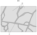
- FIG. 2 is a schematic plan view of a light-emitting layer according to the first embodiment.
- 5A to 5C are cross-sectional views showing process steps in a method for manufacturing the display device according to the first embodiment.
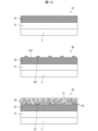
- 5A to 5C are cross-sectional views illustrating other process steps in the manufacturing method of the display device according to the first embodiment.
- 3A to 3C are schematic cross-sectional views of a hole transport layer and a light-emitting layer for illustrating a method for forming recesses according to the first embodiment.
- FIG. 11 is a schematic cross-sectional side view of a display device according to a second embodiment.
- 10 is a flowchart of a method for manufacturing a display device according to a second embodiment.
- 6A to 6C are cross-sectional views showing process steps in a method for manufacturing a display device according to a second embodiment.
- FIG. 11 is a schematic cross-sectional side view of a display device according to a third embodiment.
- FIG. 11 is a schematic cross-sectional side view of a display device according to a fourth embodiment.
- FIG. 13 is a schematic cross-sectional side view of a display device according to a fifth embodiment.
- FIG. 13 is a schematic cross-sectional side view of a display device according to a sixth embodiment. 13 is a flowchart of a method for manufacturing a display device according to a sixth embodiment.
- FIG. 13 is a schematic cross-sectional side view of a display device according to a seventh embodiment.
- FIG. 2 is a schematic diagram of a display device 1 according to this embodiment.
- the display device 1 is a device that can be used, for example, as a display for a television or a smartphone.
- the display device 1 comprises a display unit DA including a plurality of sub-pixels X, and a driver circuit DR that drives the plurality of sub-pixels X.
- At least one of the plurality of sub-pixels X comprises a light-emitting element 2 and a pixel circuit PC that drives the light-emitting element 2.
- the display device 1 performs display on the display unit DA by controlling light emission from each of the plurality of light-emitting elements 2 formed in the display unit DA via the driver circuit DR and the pixel circuit PC.
- FIG. 1 is a schematic side cross-sectional view of the display device 1 according to an embodiment of the present disclosure, and in particular shows a cross section perpendicular to the display surface of the display device 1 and passing through the light-emitting element 2. Note that the cross-sectional views of each process of the display device in the present disclosure show cross sections corresponding to the cross section of the display device 1 shown in FIG. 1.
- the display device 1 includes a display unit DA that includes the above-mentioned multiple light-emitting elements 2 and a substrate 3, and in particular multiple light-emitting elements 2 on the substrate 3.
- the display device 1 has a structure in which each layer of the light-emitting elements 2 is stacked on the substrate 3 on which, for example, a TFT (Thin Film Transistor) (not shown) is formed as a pixel circuit PC.
- TFT Thin Film Transistor
- the light-emitting element 2 includes, on an anode 21 as a first electrode, a hole transport layer 22, a light-emitting layer 23 as a first light-emitting layer, an electron transport layer 24 as a first charge transport layer, and a cathode 25 as a second electrode, in this order from the substrate 3 side.
- the anode 21 of the light-emitting element 2 is electrically connected to the TFT of the substrate 3.
- the anode 21 and the cathode 25 contain a conductive material and are electrically connected to the hole transport layer 22 and the electron transport layer 24, respectively.
- At least one of the anode 21 and the cathode 25 is a transparent electrode that transmits visible light.
- the transparent electrode include ITO (indium tin oxide), IZO (indium zinc oxide), ZnO, AZO (aluminum doped zinc oxide, also called ZAO), BZO (boron doped zinc oxide), and FTO (fluorine doped tin oxide).
- the transparent electrode may be formed by a sputtering method or the like.
- Either the anode 21 or the cathode 25 may contain a metal material, and the metal material is preferably Al, Cu, Au, Ag, or Mg alone or an alloy of these, which have a high reflectance of visible light.
- the hole transport layer 22 is a layer containing a hole transport material that transports holes from the anode 21 to the light emitting layer 23.
- a hole transport material that transports holes from the anode 21 to the light emitting layer 23.
- the hole transport layer 22 may contain at least one of polyvinylcarbazole (PVK) and [N,N'-bis(4-butylphenyl)-N,N'-bis(phenyl)-benzidine] (TPD) as the hole transport material.
- conductive compounds such as 4,4'-bis(carbazol-9-yl)biphenyl (CBP), polyphenylenevinylene (PPV), a composite of poly(3,4-ethylenedioxythiophene) (PEDOT) and polystyrenesulfonic acid (PSS) (PEDOT-PSS), poly[(9,9-dioctylfluorenyl-2,7-diyl)-co-(4,4'-(N-4-sec-butylphenyl)diphenylamine)]) (TFB) can be used.
- CBP 4,4'-bis(carbazol-9-yl)biphenyl
- PV polyphenylenevinylene
- PDOT-PSS polystyrenesulfonic acid
- TFB poly[(9,9-dioctylfluorenyl-2,7-diyl)-co-(4,4'-(N-4-sec-butylphenyl)diphen
- metal oxides such as molybdenum oxide, NiO, Cr 2 O 3 , MgO, MgZnO, LaNiO 3 , MoO 3 , or WO 3 can be used.
- materials with large electron affinity and ionization potential are suitable for the material of the hole transport layer 22.
- the electron transport layer 24 is a layer containing an electron transport material that transports electrons from the cathode 25 to the light emitting layer 23.
- the material of the electron transport layer 24 can be an organic or inorganic material that has been conventionally used in light emitting devices containing quantum dots.
- the electron transport layer 24 may contain at least one of zinc oxide (ZnO), zinc magnesium oxide (ZnMgO), titanium oxide (TiO), and tungsten oxide (WO 3 ) as the electron transport material, or may contain an inorganic nanoparticle material that is a nanoparticle of these inorganic materials.
- the electron transport layer 24 may contain an organic material such as tris(8-quinolinol)aluminum complex (Alq3), bathocuproine (BCP), or (2-(4-biphenylyl)-5-(4-tert-butylphenyl)-1,3,4-oxadiazole) (t-Bu-PBD) as the electron transport material.
- Organic material such as tris(8-quinolinol)aluminum complex (Alq3), bathocuproine (BCP), or (2-(4-biphenylyl)-5-(4-tert-butylphenyl)-1,3,4-oxadiazole) (t-Bu-PBD)
- Metal oxides such as ZnO, ZAO, ITO, InGaZnO, or electride may be used as the inorganic material of the electron transport layer 24.
- materials with small electron affinity are preferable as the material of the electron transport layer 24.
- the hole transport layer 22 and the electron transport layer 24 can be formed by a vacuum deposition method, a sputtering method, or a coating formation method using a colloidal solution using the above-mentioned materials.
- the light-emitting element 2 may also have a hole injection layer between the anode 21 and the hole transport layer 22, and an electron injection layer between the cathode 25 and the electron transport layer 24.
- the light-emitting element 2 may also have an intermediate layer between the hole transport layer 22 and the light-emitting layer 23, or between the electron transport layer 24 and the light-emitting layer 23.
- These hole injection layer, electron injection layer, and intermediate layer may all be formed by the same method as the hole transport layer 22 or the electron transport layer 24.
- Fig. 3 is a schematic diagram showing an enlarged view of the light-emitting layer 23 and the vicinity of the light-emitting layer 23 in the cross section shown in Fig. 1, particularly of region E shown in Fig. 1.
- the light-emitting layer 23 includes a plurality of quantum dots 30 and an inorganic matrix 31.
- the quantum dots 30 may be, for example, quantum dots with a core/shell structure having a core and a shell formed around the core.
- the quantum dots 30 are, for example, luminescent semiconductor nanoparticles that emit light due to excitons generated by the recombination of injected electrons and holes.
- the recombination of electrons and holes in the quantum dots 30 occurs mainly in the core.
- the core of the quantum dots 30 is a luminescent material that has a valence band level and a conduction band level and emits light due to the recombination of holes in the valence band level and electrons in the conduction band level.
- the light emitted from the quantum dots 30 has a narrow spectrum due to the quantum confinement effect, so it is possible to obtain light of a relatively deep chromaticity.
- the shell has the function of suppressing the occurrence of defects or dangling bonds in the core and reducing the recombination of carriers that undergo a deactivation process.
- the quantum dot 30 may contain materials for the core and shell that are used for the core and shell materials of conventionally known quantum dots having a core/shell.
- the quantum dot 30 may have, for example, InP/ZnS, CdSe/ZnS, CdSe/ZnSe, CdSe/CdS, ZnSe/ZnS, or CIGS/ZnS as a core/shell structure.
- the shell may be formed from multiple layers that contain multiple different materials.
- the particle size of the quantum dots 30 is approximately 1 to 100 nm.
- the wavelength of light emitted from the quantum dots 30 can be controlled by the particle size.
- the wavelength of light emitted from the quantum dots 30 can be controlled by controlling the particle size of the core. Therefore, by controlling the particle size of the quantum dots 30, the wavelength of light emitted by the display device 1 can be controlled.
- FIG. 4 Schematic diagrams 401 and 402 in FIG. 4 are schematic diagrams for showing the inorganic matrix 31 filling the spaces between the quantum dots 30.
- the schematic diagrams 401 and 402 are diagrams showing two examples of a set P of two quantum dots 30 and a region (space) K between them shown in FIG. 3.
- the schematic diagrams 401 and 402 are diagrams showing sets P1 and P2, which are examples of sets of quantum dots 30A and quantum dots 30B, respectively.
- the inorganic matrix 31 fills the spaces between the multiple quantum dots 30, it is sufficient to understand that the inorganic matrix 31 fills at least the region K between the quantum dots 30A and 30B, as shown in the schematic diagram 401 of the set P1 in FIG. 4.
- the region K is a region that is surrounded by two straight lines (common circumscribing lines) that are tangent to the outer peripheries of the quantum dots 30A and 30B, and the opposing outer peripheries of the quantum dots 30A and 30B, in the cross section of the light-emitting layer 23. Therefore, as shown in the schematic diagram 402 of the set P2 in FIG. 4, the region K can exist even if the quantum dots 30A and 30B are close to each other, and the inorganic matrix 31 fills the region K.
- the inorganic matrix 31 filling the gaps between the quantum dots 30 does not necessarily mean that the region K between the quantum dots 30A and 30B is entirely made of the inorganic matrix 31.
- the region K between the quantum dots 30A and 30B may contain a material such as a ligand that is different from the material of the inorganic matrix 31.
- the light-emitting layer 23 may contain an organic ligand that is added to improve the dispersibility of the quantum dots 30 in the dispersion liquid used for coating and that is coordinated to the outer surface of the quantum dots 30 in the dispersion liquid.
- the weight ratio of the organic ligand to the total weight including the region K may be less than 5%.
- the inorganic matrix 31 may fill the areas of the light-emitting layer 23 other than the multiple quantum dots 30.
- the outer edge (top and bottom) of the light-emitting layer 23 may be covered with the inorganic matrix 31.
- a portion of the inorganic matrix 31 may extend from the outer edge of the light-emitting layer 23, and the quantum dots 30 may be positioned away from the outer edge.
- the outer edge of the light-emitting layer 23 may not be formed only by the inorganic matrix 31, and some of the quantum dots 30 may be exposed from the inorganic matrix 31.
- the inorganic matrix 31 may refer to the portion of the light-emitting layer 23 other than the multiple quantum dots 30.
- the inorganic matrix 31 may have a continuous film having an area of 1000 nm2 or more in a plane direction perpendicular to the thickness direction at any position in the thickness direction of the light-emitting layer 23.
- the quantum dots 30 may be encapsulated in the continuous film of the inorganic matrix 31.
- the quantum dots 30 contained in the light-emitting layer 23 can be said to be encapsulated in the inorganic matrix 31.
- the light-emitting layer 23 containing the quantum dots 30 encapsulated in the inorganic matrix 31 has improved light-emitting properties and a longer lifespan.
- the light-emitting layer 23 may contain one or more quantum dots 30 per 1000 nm2 at any position in the film thickness direction in a plane direction perpendicular to the film thickness direction.
- the light-emitting layer 23 generally contains quantum dots 30 at a concentration sufficient to function as a light-emitting layer of a light-emitting element.
- the inorganic matrix 31 may be positioned, for example, all around the quantum dot 30.
- the inorganic matrix 31 in any cross section passing through any quantum dot 30, the inorganic matrix 31 may be positioned all around the quantum dot 30.
- the inorganic matrix 31 is positioned all around the quantum dot 30 may mean that the inorganic matrix 31 is positioned over 90% or more of the periphery of the quantum dot 30.
- the surface of the quantum dot 30 and the inorganic matrix 31 may be in contact.
- the band gap of the inorganic matrix 31 may be wider than the band gap of the constituent material of the quantum dot 30. If the quantum dot 30 has a core and a shell surrounding the core, the band gap of the inorganic matrix 31 may be wider than the band gap of the constituent material of the shell.
- the inorganic matrix 31 may include an inorganic material.
- the inorganic matrix may include a metal sulfide, a metal oxide, or silicon oxide (SiO 2 ).
- the inorganic matrix may also include at least one of a II-VI compound, a group II oxide, a group III oxide, and a group IV oxide.
- atom does not only mean that it exists as a single atom, but also includes those that exist in the form of a molecule having two or more atoms, including the atom in question and another atom, those that exist in the form of a complex, those that exist in the form of a compound, or those that exist in the form of an ion, and does not limit the form of existence.
- oxygen atoms include those that exist in the form of a compound having an oxygen atom, and those that exist in the form of an oxygen ion. It is preferable that oxygen atoms can be identified by analysis regardless of the form of their existence.
- the inorganic matrix 31 may also be a dense discontinuous film having at least one discontinuity.
- the "discontinuity" may be a region where one or more types of atoms constituting the inorganic matrix 31 are missing, and may typically have a size of more than 8 nm.
- the discontinuity may three-dimensionally penetrate the inorganic matrix 31.
- the discontinuity may include a gap between the multiple parts.
- the "dense discontinuous film” may mean a film having discontinuities and in which the regions other than the discontinuities are dense.
- the inorganic matrix 31 may include a continuous film with a non-uniform thickness.
- the quantum dots 30 in the light-emitting layer 23 may be regularly arranged in the light-emitting layer 23, or may be included in the light-emitting layer 23 in a disorderly manner.
- an inorganic matrix 31, which will be described later, is formed between two quantum dots 30, and the quantum dots 30 are not in contact with each other.
- the light-emitting layer 23 may include two or more quantum dots 30 that are in contact with each other.
- the film thickness of the light-emitting layer 23 may be about 1 nm to 100 nm.
- the light-emitting layer 23 is formed from a quantum dot dispersion liquid containing quantum dots 30, a drying process may be included in which the quantum dot dispersion liquid is dried by heating.
- the drying process for example, the laminate containing the quantum dot dispersion liquid applied onto the hole transport layer 22 is heated to 80°C to 150°C. Therefore, in this embodiment, from the viewpoint of the heat resistance of the light-emitting element 2, all layers of the light-emitting element 2 from the anode 21 to the cathode 25 may be formed of inorganic layers.
- the light-emitting layer 23 has a recess 32 as a first recess recessed toward the anode 21 on the surface on the cathode 25 side.
- a virtual plane VS is assumed to be a planar extension of the top surface 23T, which is the surface that contacts the electron transport layer 24 on the cathode 25 side of the light-emitting layer 23.
- the recess 32 is formed in a portion located on the anode 21 side of the virtual plane VS. Therefore, when the material that constitutes the electron transport layer 24 located on the anode 21 side of the virtual plane VS can be confirmed, the material may be considered to be located inside the recess 32.
- FIG. 5 is an enlarged plan view of the light-emitting layer 23, particularly an enlarged plan view in the above-mentioned virtual plane.
- the recesses 32 may be formed randomly on the cathode 25 side of the light-emitting layer 23.
- the light-emitting layer 23 may have at least one closed region 23E surrounded by the recesses 32 in a plan view.
- At least one closed region 23E may include 10 5 to 10 8 quantum dots 30. Note that the closed region 23E in the present disclosure is preferably observed in a plan view in a virtual plane.
- the display device 1 may include a light-emitting element 2 for each subpixel, and the light-emitting layer 23 of each light-emitting element 2 may emit light of a color corresponding to each subpixel.
- the display device 1 may include, as the light-emitting elements 2, a red light-emitting element formed in the red subpixel, a green light-emitting element formed in the green subpixel, and a blue light-emitting element formed in the blue subpixel. In this case, the display device 1 can display full color by driving each light-emitting element 2 individually.
- Fig. 6 is a band diagram of the light-emitting layer 23 and the electron transport layer 24 among the layers of the light-emitting element 2.
- Fig. 6 shows the band gap between the quantum dots 30 and the inorganic matrix 31 of the light-emitting layer 23 and the electron transport layer 24, with the higher energy side of the electrons being the upper side as viewed in the plane of the paper.
- Fig. 6 also shows the band diagram in the portion where the light-emitting layer 23 and the electron transport layer 24 are in direct contact with each other.
- the quantum dots 30 are encapsulated in the inorganic matrix 31. Therefore, as shown in FIG. 6, the electron transport layer 24 contacts the inorganic matrix 31 of the light-emitting layer 23.
- the inorganic matrix 31 has a larger band gap than the quantum dots 30, the barrier to electron injection from the electron transport layer 24 to the inorganic matrix 31 is high. Therefore, in order to drive the light-emitting element 2 and inject electrons from the electron transport layer 24 into the quantum dots 30, it is necessary to cause the electrons to tunnel through the inorganic matrix 31.
- the band gap of the electron transport layer 24 in the vicinity of the interface with the inorganic matrix 31 is effectively curved downward. Therefore, as shown in FIG. 6, a quantum well 24W with a lower level than the surrounding area is formed on the upper end of the band gap of the electron transport layer 24 on the side of the light emitting layer 23.
- electrons ET injected from the cathode 25 into the electron transport layer 24 by driving the light-emitting element 2 may accumulate on the light-emitting layer 23 side of the electron transport layer 24, particularly in the quantum well 24W.
- the accumulated electrons ET may remain in the vicinity of the light-emitting layer 23 side of the electron transport layer 24 even when driving of the light-emitting element 2 is stopped.
- the accumulation of electrons ET may reduce the efficiency of electron injection into the quantum dots 30 in the light-emitting layer 23.
- the accumulated electrons ET may deteriorate the material of the light-emitting layer 23 or the layers surrounding the light-emitting layer 23 by generating Auger electrons, etc., and may shorten the life of the light-emitting element 2.
- the light-emitting layer 23 has a recess 32 on the cathode 25 side, and a part of the material constituting the electron transport layer 24 is located inside the recess 32. Therefore, in the light-emitting element 2 of this embodiment, even if the accumulation of electrons ET described above occurs, the electrons ET are quickly released to the cathode 25 side via the electron transport layer 24 inside the recess 32 by stopping the operation of the light-emitting element 2. Therefore, the light-emitting element 2 of this embodiment reduces the electrons ET that accumulate at the interface between the light-emitting layer 23 and the electron transport layer 24, improving the light-emitting efficiency or extending the life. A display device 1 including the light-emitting element 2 reduces power consumption or extends the life.
- the light-emitting layer 23 of the light-emitting element 2 according to this embodiment has an inorganic matrix 31 that fills the spaces between the multiple quantum dots 30. Therefore, in the light-emitting element 2, the inorganic matrix 31 protects the quantum dots 30 from foreign matter such as moisture, but the accumulation of electrons between the electron transport layer 24 and the inorganic matrix 31 may become significant.
- the light-emitting layer 23 of the light-emitting element 2 according to this embodiment has a recess 32 on the electron transport layer 24 side, so that the quantum dots 30 can be protected by the inorganic matrix 31 while more efficiently releasing electrons accumulated between the electron transport layer 24 and the inorganic matrix 31.
- the maximum width of the recess 32 in the in-plane direction of the light-emitting layer 23 is 1 ⁇ m, and the depth of the recess 32 in the film thickness direction of the light-emitting layer 23 is 20 nm.
- the cross-sectional area of the recess 32 in a cross section parallel to the film thickness direction of the light-emitting layer 23 is about 5000 nm2 .
- the electron transport layer 24 has ZnO nanoparticles with a median particle size of 6 nm.
- the material of the electron transport layer 24 fills the inside of the recess 32 and the number of ZnO nanoparticles located inside the recess 32 is minimal, the nanoparticles are considered to be aligned in a line from the bottom to the top of the recess 32.
- the number inside the recess 32 is approximately 3.3.
- the total cross-sectional area of the 3.3 nanoparticles having a particle size of 6 nm is about 93.3 nm2 . Therefore, when the number of nanoparticles located inside the recess 32 is a minimum, the ratio of the total cross-sectional area of the nanoparticles to the cross-sectional area of the recess 32 is about 1.9%.
- the material constituting the electron transport layer 24 is confirmed to be present in 1.9% or more of the portion that is located closer to the anode 21 than the imaginary plane VS and that contains a material different from the material constituting the light-emitting layer 23, then the material may be considered to fill the inside of the recess 32.
- the film thickness direction of the light-emitting layer 23 is the first direction D1, and the direction perpendicular to the first direction is the second direction D2.
- at least one quantum dot 30 may overlap the recess 32 in the second direction D2.
- the quantum dot 30 included in the closed region 23E is surrounded three-dimensionally by the recess 32, and is surrounded in particular in the second direction D2. This allows the light-emitting element 2 to more efficiently release electrons accumulated near the quantum dot 30 to the material located inside the recess 32, thereby more efficiently releasing the electrons.
- the light-emitting layer 23 may include an inorganic matrix 31 between the recesses 32 and the quantum dots 30. This reduces the quantum dots 30 exposed from the recesses 32 in the light-emitting element 2, improving the protective effect of the inorganic matrix 31 on the quantum dots 30.
- the layer thickness of the inorganic matrix 31 between the recesses 32 and the quantum dots 30 corresponds to the shortest distance L1 between the recesses 32 and the quantum dots 30. From the viewpoint of more reliably suppressing exposure of the quantum dots 30 from the recesses 32, the distance L1 may be 2 nm or more.
- the light-emitting layer 23 may include an inorganic matrix 31 between the end 32E of the recess 32 on the anode 21 side and the bottom surface 23U, which is the surface on the anode 21 side, and may further include quantum dots 30. This allows the light-emitting element 2 to suppress short-circuiting between the hole transport layer 22 and the electron transport layer 24 that occurs when the recess 32 comes into contact with the hole transport layer 22. From the viewpoint of more reliably suppressing short-circuiting between the hole transport layer 22 and the electron transport layer 24, the distance L2 between the end 32E and the bottom surface 23U may be 5 nm or more.
- the maximum width of the recess 32 in the second direction D2, or the width L3 at the end of the recess 32 on the electron transport layer 24 side corresponds to the width of the recess 32 in the above-mentioned imaginary plane VS, and may be 1 ⁇ m or more and 10 ⁇ m or less. This allows the light-emitting element 2 to release the above-mentioned accumulated electrons more efficiently, while ensuring an area where the light-emitting layer 23 and the electron transport layer 24 are in contact, and improving the efficiency of electron injection into the light-emitting layer 23.
- the maximum depth L4 of the recess 32 in the first direction corresponds to the distance between the imaginary plane VS and the end 32E.
- the maximum depth L4 may be less than the layer thickness of the light-emitting layer 23 in the first direction D1. This prevents short circuits between the hole transport layer 22 and the electron transport layer 24 in the light-emitting element 2, improving the luminous efficiency of the light-emitting layer 23.
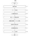
- Fig. 7 is a flow chart showing the method for manufacturing the display device 1 according to this embodiment.
- the substrate 3 is prepared (step S3).
- the substrate 3 may be manufactured, for example, by forming a plurality of the pixel circuits PC described above on a glass substrate.
- the light-emitting element 2 is formed on the substrate 3.
- the anode 21 is formed on the substrate 3 by any of the methods described above (step S2).
- the anode 21 may be formed in an island shape for each pixel circuit PC.
- the hole transport layer 22 is formed by any of the methods described above (step S3).
- the hole transport layer 22 may be formed in common for the multiple anodes 21, or may be formed in an island shape for each anode 21.
- the material of the hole transport layer 22 may differ depending on the emission color of the sub-pixel.
- FIG. 8 and FIG. 9 are process cross-sectional views showing the manufacturing method of the display device 1, and in particular show the process of forming the light-emitting layer 23 and the electron transport layer 24 in detail. Note that each process cross-sectional view in this disclosure, including FIG. 8 and FIG. 9, shows a cross section corresponding to the cross section of the display device 1 shown in FIG. 1.
- a quantum dot dispersion liquid 23A which is a dispersion liquid in which quantum dots 30 and precursors 31A of the inorganic matrix 31 are dispersed in a liquid, is applied (step S4).
- the laminate from the substrate 3 to the hole transport layer 22 is regarded as a substrate, and the quantum dot dispersion liquid 23A is applied to the substrate by various application methods such as spin coating.
- a thin film of the inorganic matrix 31 may be formed on the hole transport layer 22 prior to application of the quantum dot dispersion liquid 23A.
- the quantum dot dispersion liquid 23A may be prepared before step S4.
- the quantum dot dispersion liquid 23A may be prepared, for example, by stirring a dispersion liquid of quantum dots 30 coordinated with organic ligands and a dispersion liquid of precursor 31A to obtain a dispersion liquid of quantum dots 30 coordinated with precursor 31A.
- the precursor 31A may contain, for example, 3-(mercaptopropyl)trimethoxysilane (MPS) or tetramethyl orthosilicate (TMOS) as a precursor of silicon oxide.
- MPS 3-(mercaptopropyl)trimethoxysilane
- TMOS tetramethyl orthosilicate
- the precursor 31A is transformed into an inorganic matrix 31 by, for example, heating the applied quantum dot dispersion liquid 23A (step S5).
- a light-emitting material layer 23B is formed that includes a plurality of quantum dots 30 and an inorganic matrix 31 that fills the spaces between the plurality of quantum dots 30.
- FIG. 10 is a schematic diagram of a cross section of the hole transport layer 22 and the light-emitting material layer 23B or the light-emitting layer 23 to illustrate the method of forming recesses 32.
- step S6 the light-emitting material layer 23B is formed on the hole-transport layer 22.
- the laminate on the substrate 3 including the hole-transport layer 22 and the light-emitting material layer 23B is heated and then rapidly cooled.
- the laminate may be heated from room temperature to 130°C, held at the heating temperature for 5 minutes, and then cooled to room temperature in about 1 minute.
- the above-mentioned heating causes the hole transport layer 22 and the light emitting material layer 23B to thermally expand
- the above-mentioned rapid cooling causes the hole transport layer 22 and the light emitting material layer 23B to attempt to restore their original shapes. Therefore, the above-mentioned rapid cooling causes stress F1 in the hole transport layer 22 and stress F2 in the light emitting material layer 23B, as shown in step S6-2 of FIG. 10. Stresses F1 and F2 occur in the directions that cause the hole transport layer 22 and the light emitting material layer 23B to contract, respectively.
- the inorganic matrix 31 containing silicon oxide etc. has a lower rate of thermal expansion than the material contained in the hole transport layer 22. Therefore, stress F2 tends to be smaller than stress F1. Therefore, the above-mentioned rapid cooling generates a difference in the stresses generated in the hole transport layer 22 and the light emitting material layer 23B, and in particular, compressive stress occurs near the interface between the hole transport layer 22 and the light emitting material layer 23B, and tensile stress occurs near the upper surface of the light emitting material layer 23B.
- the above heating step may be performed by rapid heating from room temperature to 130°C in about one minute, for example.
- step S6-3 of FIG. 10 part of the inorganic matrix 31 will break from the top surface side that is not joined to the hole transport layer 22.
- a recess 32 is formed in the light-emitting material layer 23B, recessed in the direction from the surface on the side opposite the hole transport layer 22 toward the hole transport layer 22, and a light-emitting layer 23 having the recess 32 is formed.
- step S6 deterioration of the materials that make up the light-emitting layer 23, such as the quantum dots 30, can be reduced compared to when the recess 32 is directly formed by etching the light-emitting material layer 23B, for example.
- the modification of the precursor 31A to the inorganic matrix 31 and the formation of the recesses 32 may be performed in the same process.
- the applied quantum dot dispersion liquid 23A may be rapidly heated and then rapidly cooled, thereby forming the recesses 32 while modifying the precursor 31A to the inorganic matrix 31.
- the electron transport layer 24 is formed (step S7).
- the electron transport layer 24 is formed by forming a layer of the material constituting the electron transport layer 24 on the upper surface of the light-emitting layer 23 on the side of the recesses 32 by a coating method, a vapor deposition method, or the like.
- the material constituting the electron transport layer 24 is also formed inside the recesses 32.
- the formation of the electron transport layer 24 and the formation of the material constituting the electron transport layer 24 inside the recesses 32 can be performed in the same process.
- the electron transport layer 24 may be formed in common to the multiple anodes 21, as with the hole transport layer 22, or may be formed for each anode 21.
- a cathode 25 is formed on the electron transport layer 24 by the various methods described above (step S8).
- the cathode 25 may be formed in common for multiple anodes 21. In this manner, a display device 1 having light-emitting elements 2 on a substrate 3 is manufactured.
- ⁇ Evaluation of Light-emitting Device> In order to verify the characteristics of the light-emitting device 2 according to this embodiment, light-emitting devices according to an example, a comparative example 1, and a comparative example 2 were manufactured.
- the light-emitting device according to the example has the same configuration as the light-emitting device according to this embodiment.
- the light-emitting device according to the comparative example 1 has the same configuration as the light-emitting device according to this embodiment, except that the light-emitting layer 23 does not have a recess 32.
- the light-emitting device according to the comparative example 2 has the same configuration as the light-emitting device according to this embodiment, except that the light-emitting layer 23 does not have an inorganic matrix 31, and an organic ligand is coordinated to each quantum dot 30.
- ITO In the manufacturing method of the light-emitting element according to the embodiment, first, ITO was formed on a substrate by sputtering to form an anode 21. Next, a hole injection layer containing NiO was formed on the anode 21 by spin coating and baking. Next, an organic SAM (Self Assemble Monolayer) film was formed on the hole injection layer by spin coating and baking. Next, an organic hole transport material layer was formed on the SAM film by spin coating and baking. This formed a hole transport layer 22 containing a SAM film and a hole transport material layer.
- ITO In the manufacturing method of the light-emitting element according to the embodiment, first, ITO was formed on a substrate by sputtering to form an anode 21. Next, a hole injection layer containing NiO was formed on the anode 21 by spin coating and baking. Next, an organic SAM (Self Assemble Monolayer) film was formed on the hole injection layer by spin coating and baking. Next, an organic hole transport material layer was formed on the
- a thin film of ZnS was formed on the hole transport layer 22, and then a quantum dot dispersion liquid 23A containing quantum dots 30 coordinated with MPS, which is a precursor 31A, was applied on the ZnS thin film and baked.
- the laminate including the light-emitting material layer 23B was rapidly heated and then rapidly cooled by the method described above, to form recesses 32 in the light-emitting material layer 23B, thereby forming the light-emitting layer 23.
- a dispersion liquid in which nanoparticles of the electron transport material are dispersed was applied onto the light-emitting layer 23 by a spin coating method, and the resulting mixture was baked, to form the electron transport layer 24.
- a cathode 25 was formed on the electron transport layer 24 by a vacuum deposition method, thereby producing the light-emitting device according to the example.
- the light-emitting element according to Comparative Example 1 was manufactured by the same method as the light-emitting element according to the above-mentioned Example, except that the light-emitting material layer 23B was not rapidly heated or cooled. Therefore, in the method of manufacturing the light-emitting element according to the Comparative Example, the light-emitting material layer 23B without the recess 32 became the light-emitting layer as it is.
- the light-emitting element according to Comparative Example 2 was manufactured by the same method as the light-emitting element according to the above-mentioned Example, except that the light-emitting layer 23 was formed by applying and baking a dispersion of quantum dots 30 coordinated with organic ligands.
- the light-emitting element according to the Example has improved reliability compared to the light-emitting elements according to Comparative Examples 1 and 2.
- the light-emitting element according to the Example exhibits a reduction in luminance, which is believed to be due to the accumulation of electrons near the interface between the light-emitting layer 23 and the electron transport layer 24, which is resolved more quickly when the operation of the light-emitting element is stopped, compared to the light-emitting elements according to each of the Comparative Examples.
- the light-emitting element according to the Example has a lower concentration of organic ligands in the light-emitting layer 23 compared to the light-emitting element according to Comparative Example 2.
- the light-emitting element according to the Example has a light-emitting layer 23 with reduced organic ligands that strongly capture electrons, and therefore electrons accumulated near the interface between the light-emitting layer 23 and the electron transport layer 24 are released more quickly.
- the number of quantum dots 30 in the closed region 23E surrounded by the recess 32 was considered as follows.
- the light-emitting layer 23 of the light-emitting element according to the embodiment was observed in a virtual plane VS, five closed regions 23E including closed region 1 to closed region 5 were identified, and the area of each closed region 23E was calculated.
- the area of each closed region 23E was calculated by obtaining an image of the cross section of the observed light-emitting layer 23, identifying the boundary of the closed region 23E from the brightness and darkness of the image, and measuring the number of pixels contained in the closed region 23E.
- the boundary of the closed region 23E may also be identified by observing a cross section parallel to the film thickness direction of the light-emitting layer 23.
- the number of quantum dots 30 contained in each closed region 23E is calculated by dividing the area of the closed region 23E by the cross-sectional area of the cross-section passing through the center of the quantum dot 30.
- any cross-section of the light-emitting layer 23 is observed by a TEM (transmission electron microscope) at a magnification of 200,000 times or more, the average particle diameter D of at least 500 quantum dots 30 is calculated, and ⁇ (D/2) 2 is set as the cross-sectional area of the quantum dots 30.
- the maximum width of the observed quantum dots 30 is set as the particle diameter of the quantum dots 30.
- the “Closed region area” column indicates the area of each closed region 23E.
- the “QD emission color” column indicates the emission color of the quantum dots 30 contained in each closed region 23E.
- the quantum dots 30 whose emission color is “red” have an average particle size D of 10 nm and a cross-sectional area of 78.5 nm2 .
- the quantum dots 30 whose emission color is “green” have an average particle size D of 5 nm and a cross-sectional area of 19.6 nm2 .
- the quantum dots 30 whose emission color is “blue” have an average particle size D of 6 nm and a cross-sectional area of 28.3 nm2 .
- the "QD number” column indicates the number of quantum dots 30 contained in each closed region 23E when the emission color of the quantum dots 30 is the color indicated by "QD emission color”.
- the number of quantum dots 30 contained in each of the closed regions 1 to 5 is 10 5 or more and 10 9 or less. This corresponds to the number of quantum dots 30 surrounded by the recess 32 being 10 5 or more and 10 9 or less. Since the number of quantum dots 30 contained in the closed region 23E is 10 5 or more, the light-emitting element 2 can more efficiently emit light in the closed region 23E.
- the outer peripheral area of a group of quantum dots 30 surrounded by the recess 32 is proportional to the 1/3 power of the number of the group of quantum dots 30. Therefore, the outer peripheral area per one of the group of quantum dots 30 is proportional to the ⁇ 1/3 power of the number of the group of quantum dots 30.
- step S6 by adjusting the heating and cooling speed in step S6, the difference in stress between the hole transport layer 22 and the light emitting material layer 23B can be adjusted, and thus the number or spacing of the recesses 32 formed can be adjusted.
- the size of each closed region 23E can be adjusted, and in combination with adjusting the particle size of the quantum dots 30 contained in the light emitting layer 23, the number of quantum dots 30 contained in each closed region 23E can be adjusted.
- FIG. 11 is a schematic side cross-sectional view of a display device 4 according to another embodiment of the present disclosure.
- the display device 4 according to this embodiment includes a light-emitting element 5 instead of the light-emitting element 2.
- the light-emitting element 5 includes a light-emitting layer 26 instead of the light-emitting layer 23.
- the light-emitting layer 26 has a recess 33 instead of the recess 32.
- the recess 33 is located on the surface on the anode 21 side, and is recessed towards the cathode 25 side.
- a part of the material constituting the hole transport layer 22 is located inside the recess 33.
- the display device 4 has the same configuration as the display device 1 according to the previous embodiment.
- the light-emitting element 5 has, on an anode 21 as a second electrode, a hole transport layer 22 as a first charge transport layer, a light-emitting layer 26 as a first light-emitting layer, an electron transport layer 24, and a cathode 25 as a first electrode, in this order from the substrate 3 side.
- the difference in band gap between the hole transport layer 22, the quantum dots 30, and the inorganic matrix 31 may hinder hole injection from the hole transport layer 22 to the quantum dots 30. For this reason, in the light-emitting element 5, holes may accumulate near the interface between the hole transport layer 22 and the light-emitting layer 26.
- the light-emitting layer 26 of the light-emitting element 5 has a recess 33 as a first recess on the surface on the anode 21 side, in which part of the material constituting the hole transport layer 22 is located. Therefore, in the light-emitting element 5 according to this embodiment, even if the accumulation of holes described above occurs, the holes are quickly released to the anode 21 side via the hole transport layer 22 inside the recess 33 by stopping the driving of the light-emitting element 5.
- the carrier balance in the light-emitting layer may result in an excess of holes.
- the accumulation of holes on the anode side of the light-emitting layer may become significant.
- the light-emitting element 5 of this embodiment efficiently reduces the excess of holes in the light-emitting layer 26 or the excess of holes at the interface between the hole transport layer 22 and the light-emitting layer 26 through the recess 33. Therefore, the light-emitting element 5 can efficiently achieve an improvement in light-emitting efficiency or an extension of the life span.
- FIG. 12 is a flowchart showing a method for manufacturing a display device 4 according to this embodiment. Note that, for each step shown in the flowchart of this disclosure, steps that can be executed with the same content are given the same reference numbers.
- the display device 4 according to this embodiment may be manufactured in the same manner as the manufacturing method of the display device 1 according to the previous embodiment, except that step S9 is performed after step S3 instead of step S6. Specifically, in the manufacturing method of the display device 4 according to this embodiment, after step S3, a convex portion or a concave portion serving as a fifth concave portion is formed in the hole transport layer 22 (step S9), and step S7 is performed after step S5.
- FIG. 13 is a cross-sectional view showing the steps in the manufacturing method of the display device 4, and in particular shows in detail the steps of forming convex and concave portions in the hole transport layer 22.
- step S3 of FIG. 8 When the formation of the hole transport layer 22 is completed, as shown in step S3 of FIG. 8, the anode 21 and the hole transport layer 22 are formed in this order on the substrate 3.
- step S9 of FIG. 13 in step S3, a convex portion 22P that protrudes upward, or a concave portion 22C as a fifth concave portion recessed toward the anode 21, is formed on the upper surface side of the hole transport layer 22.
- step S9 following the deposition of the hole transport layer 22, the material of the hole transport layer 22 may be imprinted onto the hole transport layer 22 to form a convex portion 22P in the hole transport layer 22.
- step S9 following the deposition of the hole transport layer 22, a portion of the hole transport layer 22 may be etched to form a concave portion 22C in the hole transport layer 22. Note that in step S9, only one of the formation of the convex portion 22P and the formation of the concave portion 22C may be performed, or both may be performed.
- steps S4 and S5 are performed to form the light-emitting layer 26 on the upper surface of the hole transport layer 22 on which the convex portion 22P or the concave portion 22C is formed.
- the light-emitting material layer formed in step S5 becomes the light-emitting layer 26 as it is.
- the shape of the lower surface of the light-emitting layer 26 reflects the shape of the upper surface of the hole transport layer 22 having the convex portion 22P or the concave portion 22C. Therefore, by performing the formation process of the light-emitting layer 26 following step S9, a concave portion 33 is formed on the surface of the light-emitting layer 26 on the anode 21 side.
- the shape of the concave portion 33 can be designed by designing the shape of the convex portion 22P or the concave portion 22C formed in step S9, the above manufacturing method makes it easier to design the shape of the concave portion 33 and improves the accuracy of the shape of the concave portion 33.
- FIG. 14 is a schematic side cross-sectional view of a display device 6 according to another embodiment of the present disclosure.
- the display device 6 according to this embodiment includes a light-emitting element 7 instead of the light-emitting element 2.
- the light-emitting element 7 includes, in this order from the substrate 3 side, a cathode 25 as a first electrode, an electron transport layer 24, a light-emitting layer 23 as a first light-emitting layer, a hole transport layer 22 as a first charge transport layer, and an anode 21 as a second electrode.
- a part of the material constituting the hole transport layer 22 is located inside the recess 32 of the light-emitting layer 23 according to this embodiment.
- each layer of the light-emitting element 7 may have the same configuration as each layer of the light-emitting element 2 except for the stacking order, and in particular may be made of the same material as each layer of the light-emitting element 2.
- the cathode 25 according to this embodiment may be formed for each pixel circuit PC, and the anode 21 may be formed in common to the multiple cathodes 25.
- the light-emitting element 7 for the same reason as described above, the holes accumulated near the interface between the light-emitting layer 23 and the hole transport layer 22 are quickly released to the anode 21 side through the hole transport layer 22 inside the recess 33. Therefore, the light-emitting element 7 can efficiently achieve improved light-emitting efficiency or longer life.
- the display device 6 may be manufactured by performing steps S1, S8, S7, S4, S5, S6, S3, and S2 in this order among the above-mentioned steps.
- step S3 a part of the material of the hole transport layer 22 is formed inside the recess 32 of the light-emitting layer 23 formed in step S6.
- FIG. 15 is a schematic side cross-sectional view of a display device 8 according to another embodiment of the present disclosure.
- the display device 8 according to this embodiment includes a light-emitting element 9 instead of the light-emitting element 7.
- the light-emitting element 9 includes a light-emitting layer 26 instead of the light-emitting layer 23. Therefore, a part of the material constituting the electron transport layer 24 is located inside the recess 33 of the light-emitting layer 26 according to this embodiment.
- the display device 8 has the same configuration as the display device 6 according to the previous embodiment.
- the light-emitting element 9 has, on a cathode 25 as a second electrode, an electron transport layer 24 as a first charge transport layer, a light-emitting layer 23 as a first light-emitting layer, a hole transport layer 22, and an anode 21 as a first electrode, in this order from the substrate 3 side.
- the light-emitting element 9 for the same reason as described above, electrons accumulated near the interface between the light-emitting layer 26 and the electron transport layer 24 are quickly released to the cathode 25 side through the electron transport layer 24 inside the recess 33. Therefore, the light-emitting element 9 can efficiently achieve improved light-emitting efficiency or longer life.
- the display device 6 may be manufactured by performing steps S1, S8, S7, S9, S4, S5, S3, and S2 in this order among the above-mentioned steps.
- step S9 convex portions or concave portions are formed in the electron transport layer 24. Therefore, in the subsequent process of forming the light-emitting layer 26, the light-emitting layer 26 reflects the shape of the convex portions or concave portions of the electron transport layer 24, and therefore concave portions 33 are formed in the light-emitting layer 26.
- ⁇ Second Recess> 16 is a schematic side cross-sectional view of a display device 10 according to another embodiment of the present disclosure.
- the display device 10 according to this embodiment includes a light-emitting element 11 instead of the light-emitting element 2.
- the light-emitting element 11 includes a light-emitting layer 27 instead of the light-emitting layer 23.
- the light-emitting layer 27 has a recess 33 as a second recess in addition to a recess 32 as a first recess.
- the light-emitting layer 27 has both a recess 32 located on the surface on the cathode 25 side and recessed toward the anode 21 side, and a recess 33 located on the surface on the anode 21 side and recessed toward the cathode 25 side. Furthermore, part of the material constituting the electron transport layer 24 as the first charge transport layer is located inside the recess 32, and part of the material constituting the hole transport layer 22 as the second charge transport layer is located inside the recess 33.
- the light-emitting element 11 In the light-emitting element 11 according to this embodiment, electrons accumulated near the interface between the light-emitting layer 27 and the electron transport layer 24 are quickly released to the cathode 25 side through the electron transport layer 24 inside the recess 32. Furthermore, in the light-emitting element 11 according to this embodiment, holes accumulated near the interface between the light-emitting layer 27 and the hole transport layer 22 are quickly released to the anode 21 side through the hole transport layer 22 inside the recess 33. In other words, the light-emitting element 11 quickly releases both the electrons and holes accumulated near the light-emitting layer 27. Therefore, the light-emitting element 11 can more efficiently achieve improved luminous efficiency or longer life.
- the inside of the recess 32 may be filled with a part of the material constituting the electron transport layer 24, and the inside of the recess 33 may be filled with a part of the material constituting the hole transport layer 22. This allows the light-emitting element 11 to more quickly release both the electrons and holes accumulated near the light-emitting layer 27, and more efficiently achieve improved light-emitting efficiency or longer life.
- the display device 10 may be manufactured by the same method, except that step S9 is further performed following step S3.
- the light-emitting material layer formed in steps S4 and S5 reflects the shape of the convex portion 22P or the concave portion 22C of the hole transport layer 22 formed in step S9, and a concave portion 33 is formed on the surface of the light-emitting material layer on the anode 21 side.
- a concave portion 32 is formed on the upper surface of the light-emitting material layer, and a light-emitting layer 27 is formed.
- FIG. 17 is a schematic side cross-sectional view of a display device 12 according to another embodiment of the present disclosure.
- the display device 12 according to this embodiment includes a light-emitting element 13 instead of the light-emitting element 2.
- the light-emitting element 13 includes a first portion 14, a charge generating layer 15, and a second portion 16 laminated in this order from the substrate 3 side.
- the first section 14 comprises, in order from the substrate 3 side, an anode 21 as a first electrode, a hole transport layer 22, a light-emitting layer 23 as a first light-emitting layer, and an electron transport layer 24 as a first charge transport layer.
- the light-emitting layer 23 of the first section 14 has a recess 32 recessed toward the anode 21 on the surface on the side of the cathode 25 of the second section 16 described below, and a part of the material of the electron transport layer 24 is located inside the recess 32. Therefore, the first section 14 may have a laminated structure in which only the cathode 25 is removed from the light-emitting element 2 described above.
- the second section 16 comprises, in order from the charge generation layer 15 side, a hole transport layer 22, a light-emitting layer 23 as a second light-emitting layer, an electron transport layer 24 as a third charge transport layer, and a cathode 25 as a second electrode.
- the light-emitting layer 23 of the second section 16 has a recess 32 as a third recess recessed toward the anode 21 of the first section 14 on the surface on the cathode 25 side, and a part of the material of the electron transport layer 24 is located inside the recess 32. Therefore, the second section 16 may have a laminated structure in which only the anode 21 is removed from the light-emitting element 2 described above.
- the charge generation layer 15 is a layer that generates charges in response to the potential difference between the anode 21 of the first section 14 and the cathode 25 of the second section 16, in other words, in response to driving of the light-emitting element 13. In particular, when the light-emitting element 13 is driven, the charge generation layer 15 injects electrons into the electron transport layer 24 of the first section 14 and injects holes into the hole transport layer 22 of the second section 16.
- the charge generation layer 15 may include, for example, an electron generation layer located on the first section 14 side and including an n-type semiconductor, and a hole generation layer located on the second section 16 side and including a p-type semiconductor.
- the charge generation layer 15 can be formed by a vacuum deposition method, a sputtering method, a coating formation method using a colloidal solution, or the like.
- the light-emitting layer 23 in the first section 14 and the light-emitting layer 23 in the second section 16 may emit light of the same color or different colors.
- the display device 12 may be provided with a color filter corresponding to the emission color of each sub-pixel on the side of the cathode 25 of the light-emitting element 13.
- the light-emitting element 13 can achieve improved luminous efficiency or longer life in both the first portion 14 and the second portion 16 while causing both the light-emitting layer 23 in the first portion 14 and the light-emitting layer 23 in the second portion 16 to emit light.
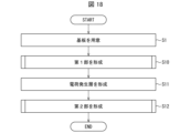
- FIG. 18 is a flowchart showing a method for manufacturing the display device 12 according to this embodiment.
- step S1 is first performed, and then the first portion 14 is formed on the substrate 3 (step S10).
- the first portion 14 may be formed by sequentially performing steps S2 to S7 of the method for manufacturing the display device 1.
- Step S11 a charge generating layer 15 is formed on the electron transport layer 24 of the first portion 14 (step S11).
- Step S11 may be performed, for example, by forming an electron generating layer and a hole generating layer in sequence by the method described above.
- the second portion 16 is formed on the charge generating layer 15 (step S12).
- the second portion 16 may be formed by sequentially performing steps S3 to S8 of the manufacturing method of the display device 1. In this manner, the display device 12 according to this embodiment is manufactured.
- the display device 12 includes a light-emitting element 13 in which a first section 14 including a first light-emitting layer and a second section 16 including a second light-emitting layer are stacked with a charge generation layer 15 interposed therebetween, but is not limited to this.
- the light-emitting element 13 may further include a charge generation layer, a hole transport layer, a third light-emitting layer, and an electron transport layer, in this order from the anode 21 side, between the electron transport layer 24 and the charge generation layer 15 of the first section 14, or between the electron transport layer 24 and the cathode 25 of the second section.
- the positions of the first light-emitting layer, the second light-emitting layer, and the third light-emitting layer may be interchanged.
- the first light-emitting layer, the second light-emitting layer, and the third light-emitting layer may emit red light, green light, and blue light, respectively, and may be formed in common across multiple sub-pixels.
- the display device 12 may be provided with a red color filter, a green color filter, and a blue color filter corresponding to each sub-pixel on the cathode 25 side of the light-emitting element 11. This allows the display device 12 to display in full color without requiring patterning of each light-emitting layer in the manufacturing process of the light-emitting element 11.
- FIG. 7 is a schematic side cross-sectional view of a display device 17 according to another embodiment of the present disclosure.
- the display device 17 according to this embodiment includes a light-emitting element 18 instead of the light-emitting element 13.
- the light-emitting element 18 includes a first portion 19 instead of the first portion 14 and a second portion 20 instead of the second portion 16.
- the first section 19 has a light-emitting layer 27 instead of the light-emitting layer 23. Therefore, the first section 19 has an anode 21 as a first electrode, a hole transport layer 22 as a second charge transport layer, a light-emitting layer 27 as a first light-emitting layer, and an electron transport layer 24 as a first charge transport layer.
- the light-emitting layer 27 of the first section 19 has a recess 33 as a second recess recessed toward the cathode 25 of the second section 20 described later on the surface on the anode 21 side, and a part of the material of the hole transport layer 22 is located inside the recess 33. Therefore, the first section 19 may have a laminated structure in which only the cathode 25 is removed from the light-emitting element 11 described above.
- the second part 20 has a light-emitting layer 27 instead of the light-emitting layer 23. Therefore, the second part 20 has a hole transport layer 22 as a fourth charge transport layer, a light-emitting layer 27 as a second light-emitting layer, an electron transport layer 24 as a third charge transport layer, and a cathode 25 as a second electrode.
- the light-emitting layer 27 of the second part 20 has a recess 33 as a fourth recess recessed toward the cathode 25 on the surface on the anode 21 side of the first part 19, and a part of the material of the hole transport layer 22 is located inside the recess 33. Therefore, the second part 20 may have a laminated structure in which only the anode 21 is removed from the above-mentioned light-emitting element 11.
- the display device 17 according to this embodiment has the same configuration as the display device 12 according to the previous embodiment. Therefore, when the light-emitting element 18 is driven, holes from the anode 21 and electrons from the charge generation layer 15 are injected into the light-emitting layer 27 of the first portion 19, and holes from the charge generation layer 15 and electrons from the cathode 25 are injected into the light-emitting layer 27 of the second portion 20. Therefore, when the light-emitting element 18 is driven, the display device 17 extracts light from both the light-emitting layer 27 of the first portion 19 and the light-emitting layer 27 of the second portion 20.
- the electrons and holes accumulated near the light-emitting layer 27 are quickly released via the charge transport material in the recesses 32 and 33, respectively. Therefore, the light-emitting element 18 can more efficiently achieve improved luminous efficiency or longer life in both the first section 19 and the second section 20 while causing both the light-emitting layer 27 in the first section 19 and the light-emitting layer 27 in the second section 20 to emit light.
- the display device 17 according to this embodiment may be manufactured by a method in which some steps of the manufacturing method of the display device 12 according to the previous embodiment are modified.
- the display device 17 may be manufactured by a method in which step S9, which follows step S3, is added to each of steps S10 and S12 of the manufacturing method of the display device 12.
Landscapes
- Physics & Mathematics (AREA)
- Optics & Photonics (AREA)
- Engineering & Computer Science (AREA)
- Manufacturing & Machinery (AREA)
- Chemical & Material Sciences (AREA)
- Crystallography & Structural Chemistry (AREA)
- Inorganic Chemistry (AREA)
- Nanotechnology (AREA)
- Electroluminescent Light Sources (AREA)
Abstract
Un élément électroluminescent (2) selon l'invention comprend une première électrode (21), une seconde électrode (25), une première couche électroluminescente (23) et une première couche de transport de charge (24). La couche électroluminescente est située entre les première et seconde électrodes, et présente des premiers évidements (32) pratiqués dans la surface du côté de la seconde électrode en direction du côté de la première électrode. La première couche de transport de charge entre en contact avec la première couche électroluminescente du côté de la seconde électrode, et une partie du matériau constituant la première couche de transport de charge est située à l'intérieur des premiers évidements.
Priority Applications (2)
| Application Number | Priority Date | Filing Date | Title |
|---|---|---|---|
| CN202380101638.1A CN121713674A (zh) | 2023-08-23 | 2023-08-23 | 发光元件、显示装置、发光元件的制造方法 |
| PCT/JP2023/030267 WO2025041293A1 (fr) | 2023-08-23 | 2023-08-23 | Élément électroluminescent, dispositif d'affichage et procédé de fabrication d'élément électroluminescent |
Applications Claiming Priority (1)
| Application Number | Priority Date | Filing Date | Title |
|---|---|---|---|
| PCT/JP2023/030267 WO2025041293A1 (fr) | 2023-08-23 | 2023-08-23 | Élément électroluminescent, dispositif d'affichage et procédé de fabrication d'élément électroluminescent |
Publications (1)
| Publication Number | Publication Date |
|---|---|
| WO2025041293A1 true WO2025041293A1 (fr) | 2025-02-27 |
Family
ID=94731819
Family Applications (1)
| Application Number | Title | Priority Date | Filing Date |
|---|---|---|---|
| PCT/JP2023/030267 Pending WO2025041293A1 (fr) | 2023-08-23 | 2023-08-23 | Élément électroluminescent, dispositif d'affichage et procédé de fabrication d'élément électroluminescent |
Country Status (2)
| Country | Link |
|---|---|
| CN (1) | CN121713674A (fr) |
| WO (1) | WO2025041293A1 (fr) |
Citations (2)
| Publication number | Priority date | Publication date | Assignee | Title |
|---|---|---|---|---|
| CN102916097A (zh) * | 2011-08-01 | 2013-02-06 | 潘才法 | 一种电致发光器件 |
| KR20230085282A (ko) * | 2021-12-06 | 2023-06-14 | 삼성디스플레이 주식회사 | 발광 소자, 발광 소자의 제조 방법 및 이를 포함하는 표시 장치 |
-
2023
- 2023-08-23 WO PCT/JP2023/030267 patent/WO2025041293A1/fr active Pending
- 2023-08-23 CN CN202380101638.1A patent/CN121713674A/zh active Pending
Patent Citations (2)
| Publication number | Priority date | Publication date | Assignee | Title |
|---|---|---|---|---|
| CN102916097A (zh) * | 2011-08-01 | 2013-02-06 | 潘才法 | 一种电致发光器件 |
| KR20230085282A (ko) * | 2021-12-06 | 2023-06-14 | 삼성디스플레이 주식회사 | 발광 소자, 발광 소자의 제조 방법 및 이를 포함하는 표시 장치 |
Also Published As
| Publication number | Publication date |
|---|---|
| CN121713674A (zh) | 2026-03-20 |
Similar Documents
| Publication | Publication Date | Title |
|---|---|---|
| KR101274068B1 (ko) | 양자점 발광 소자 및 이를 이용한 디스플레이 | |
| US10229954B2 (en) | Organic light-emitting device and organic light-emitting display device using the same | |
| CN106953020B (zh) | 一种有机发光显示器件和有机发光显示装置 | |
| JP5783780B2 (ja) | 表示装置 | |
| US20170186909A1 (en) | Quantum dot and light emitting diode including the same | |
| CN103811525A (zh) | 有机发光显示设备及制造该有机发光显示设备的方法 | |
| WO2022143770A1 (fr) | Dispositif d'affichage et procédé de préparation associé | |
| JP7818094B2 (ja) | 発光素子、表示装置、発光素子の製造方法 | |
| WO2025041293A1 (fr) | Élément électroluminescent, dispositif d'affichage et procédé de fabrication d'élément électroluminescent | |
| WO2021059472A1 (fr) | Dispositif d'éclairage | |
| US20260090232A1 (en) | Display device and method for producing display device | |
| WO2021084598A1 (fr) | Élément électroluminescent | |
| WO2021044634A1 (fr) | Dispositif d'affichage et son procédé de production | |
| WO2025224911A1 (fr) | Élément électroluminescent, dispositif d'affichage et procédé de fabrication d'un élément électroluminescent | |
| WO2025248707A1 (fr) | Élément électroluminescent, dispositif d'affichage et procédé de fabrication d'élément électroluminescent | |
| WO2025220144A1 (fr) | Élément émetteur de lumière, dispositif d'affichage et procédé de fabrication d'élément émetteur de lumière | |
| WO2025120759A1 (fr) | Élément électroluminescent, dispositif d'affichage, et procédé de production d'élément électroluminescent | |
| WO2025169384A1 (fr) | Élément électroluminescent, dispositif d'affichage et procédé de fabrication d'élément électroluminescent | |
| WO2025257964A1 (fr) | Élément électroluminescent et dispositif d'affichage | |
| WO2025203203A1 (fr) | Élément électroluminescent, dispositif d'affichage et procédé de fabrication d'élément électroluminescent | |
| WO2025257965A1 (fr) | Élément électroluminescent et dispositif d'affichage | |
| WO2025088661A1 (fr) | Élément électroluminescent, dispositif d'affichage et procédé de fabrication d'élément électroluminescent | |
| WO2024062628A1 (fr) | Élément électroluminescent, dispositif d'affichage et procédé de production d'élément électroluminescent | |
| WO2026069421A1 (fr) | Élément électroluminescent, dispositif d'affichage et procédé de production d'élément électroluminescent | |
| WO2025088660A1 (fr) | Élément électroluminescent, dispositif d'affichage et procédé de fabrication d'élément électroluminescent |
Legal Events
| Date | Code | Title | Description |
|---|---|---|---|
| 121 | Ep: the epo has been informed by wipo that ep was designated in this application |
Ref document number: 23949751 Country of ref document: EP Kind code of ref document: A1 |
|
| NENP | Non-entry into the national phase |
Ref country code: DE |