WO2025041272A1 - Atténuateur variable, atténuateur à plots et dispositif de test - Google Patents
Atténuateur variable, atténuateur à plots et dispositif de test Download PDFInfo
- Publication number
- WO2025041272A1 WO2025041272A1 PCT/JP2023/030182 JP2023030182W WO2025041272A1 WO 2025041272 A1 WO2025041272 A1 WO 2025041272A1 JP 2023030182 W JP2023030182 W JP 2023030182W WO 2025041272 A1 WO2025041272 A1 WO 2025041272A1
- Authority
- WO
- WIPO (PCT)
- Prior art keywords
- variable attenuator
- switch
- attenuator
- variable
- output
- Prior art date
- Legal status (The legal status is an assumption and is not a legal conclusion. Google has not performed a legal analysis and makes no representation as to the accuracy of the status listed.)
- Pending
Links
Images


Classifications
-
- H—ELECTRICITY
- H03—ELECTRONIC CIRCUITRY
- H03H—IMPEDANCE NETWORKS, e.g. RESONANT CIRCUITS; RESONATORS
- H03H11/00—Networks using active elements
- H03H11/02—Multiple-port networks
- H03H11/24—Frequency-independent attenuators
Definitions
- the present invention relates to a variable attenuator, a step attenuator, and a test device.
- Patent Document 1 states that "In the microwave circuit 1A, the line width step portion 32A is formed on one side of the transmission line 25A, i.e., biased in the width direction (Y direction), at the center of the transmission line 25A in the length direction (X direction)" (paragraph 44).
- Patent Document 2 states that "The high-frequency device further includes terminals P1 and P2 for inputting and outputting high-frequency signals on the pattern conductor 1, and a ground terminal GND on the pattern conductor 5.
- the pattern conductors 1, 4, and 5 and the via conductors 2 and 3 connect the terminals P1 and P2 and the ground terminal GND to form a signal line for transmitting a high-frequency signal. ...
- Patent Document 3 states that "Many semiconductor RF switches today stack multiple low BVds transistors in series to improve the breakdown performance of the entire switch" (paragraph 6).
- Patent Document 1 JP 2014-241482
- Patent Document 2 WO 2014/030469
- Patent Document 3 JP 2010-527179 A
- variable attenuator comprising a transmission line having an open stub connected between an input and an output of the variable attenuator, a first switch connected between the input and a reference potential, and a second switch connected between the output and the reference potential.
- the variable attenuator may include a first resistor connected in series with a first switch between the input and a reference potential, and a second resistor connected in series with a second switch between the output and the reference potential.
- the first resistor may be connected to the end of the first switch on the reference potential side, and the second resistor may be connected to the end of the second switch on the reference potential side.
- the open stub may be connected to a central position on the transmission line between the input and output of the variable attenuator.
- the open stub may have a length less than the length of the transmission line between the input and output of the variable attenuator.
- a step attenuator in a second aspect of the present invention, includes a plurality of cascaded variable attenuators of the first aspect.
- a test apparatus in a third aspect of the present invention, includes a test signal generating circuit that generates a test signal for testing a device under test, a comparison circuit that compares a response signal output by the device under test in response to the test signal with an expected value, and a variable attenuator of the first aspect that attenuates the test signal or the response signal.
- the test device may include a gain amplifier connected between the test signal generating circuit and the variable attenuator to amplify the test signal.
- Any of the above test devices may include a mixer connected between the comparator circuit and the variable attenuator to convert the frequency of the response signal.
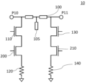
- FIG. 1 shows a configuration of a variable attenuator 10 according to the present embodiment.
- 1 shows the configuration of a modified example of the variable attenuator 10 according to the present embodiment.
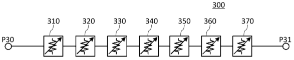
- 2 shows the configuration of a step attenuator according to the present embodiment.
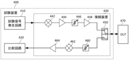
- 1 shows the configuration of a test apparatus 400 according to the present embodiment.
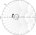
- FIG. 1 is an explanatory diagram for explaining output results of a Smith chart at each position of the variable attenuator 10 of the present embodiment.
- 4 shows the output result of the variable attenuator 10 on a Smith chart.
- 4 shows the output result of the variable attenuator 10 on a Smith chart.
- 4 shows the output result of the variable attenuator 10 on a Smith chart.
- 4 shows the output result of the variable attenuator 10 on a Smith chart.
- 4 shows the output result of the variable attenuator 10 on a Smith chart.
- FIG. 4 shows the output result of the variable attenuator 10 on a Smith chart.
- 10A and 10B are explanatory diagrams for explaining each position of a variable attenuator 500 of a reference example.
- 4 shows the output result of the variable attenuator 500 on a Smith chart.
- 4 shows the output result of the variable attenuator 500 on a Smith chart.
- 4 shows the output result of the variable attenuator 500 on a Smith chart.
- the relationship between the impedance and length of an open stub as viewed from the connection position of the transmission line is shown.
- 1 shows the results of a simulation of the state error of a variable attenuator with an attenuation of 8 dB.
- 1 shows simulation results of the insertion loss of the step attenuators in Example 2, Reference Example 2, and Reference Example 3.
- 13 shows simulation results of state errors of the step attenuators in the second embodiment, the second reference example, and the third reference example.
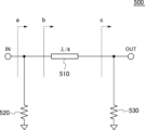
- FIG. 1 shows the configuration of a variable attenuator 10 according to this embodiment.
- the variable attenuator 10 has an input terminal P10 and an output terminal P11.
- the variable attenuator 10 attenuates, for example, a high-frequency signal input to the input terminal P10 and outputs the attenuated signal from the output terminal P11.
- the variable attenuator 10 can change the amount of signal attenuation by changing the internal resistance value.
- the variable attenuator 10 includes a transmission line 100, a first switch 110, a first resistor 120, a second switch 130, and a second resistor 140.
- the transmission line 100 is connected between an input terminal P10 and an output terminal P11.
- the transmission line 100 outputs a signal input to the input terminal P10 from the output terminal P11.
- the transmission line 100 can attenuate a high-frequency signal such as an RF signal by transmitting the high-frequency signal.
- the transmission line 100 has a straight line connecting the input terminal P10 and the output terminal P11.
- the length (electrical length) l series of the straight line may be in the range of ⁇ /8 ⁇ l series ⁇ /4, where ⁇ is the wavelength of the signal to be transmitted.
- the transmission line 100 has an open stub 105 connected between the input terminal P10 and the output terminal P11 of the variable attenuator 10.
- the open stub 105 branches off from the straight line of the transmission line 100 between the input terminal P10 and the output terminal P11, and has an open end.
- the open stub 105 may be connected to any position of the straight line between the input terminal P10 and the output terminal P11 of the transmission line 100, for example, to a center position between the input terminal P10 and the output terminal P11 of the variable attenuator 10 in the transmission line 100.
- the open stub 105 is provided for impedance conversion of the variable attenuator 10.
- the open stub 105 may have a length (electrical length) l stub that is less than the length l series of the straight line of the transmission line 100 between the input terminal P10 and the output terminal P11 of the variable attenuator 10.
- the open stub 105 may have a length l stub from the connection position (branch position) in the range of ⁇ /4>l stub (particularly ⁇ /8 ⁇ l stub ) where the impedance of the open stub 105 seen from the connection position shows capacitive properties, and may have a length l series >l stub where l series is greater than l stub , for a wavelength ⁇ of a signal to be transmitted.
- the first switch 110 is connected between the input terminal P10 and the reference potential.
- the first switch 110 switches whether or not the input terminal P10 and the reference potential are connected.
- the first switch 110 may be a shunt switch such as a HEMT (high electron mobility transistor).
- the first resistor 120 is connected in series with the first switch 110 between the input terminal P10 and the reference potential.
- the first resistor 120 may be connected to the end of the first switch 110 on the reference potential side.
- the reference potential may be a fixed potential such as ground potential (0V), and so on.
- the second switch 130 is connected between the output terminal P11 and the reference potential.
- the second switch 130 switches between connecting or not connecting the output terminal P11 and the reference potential.
- the second switch 130 may be a shunt switch such as a HEMT.
- the second resistor 140 is connected in series with the second switch 130 between the output terminal P11 and the reference potential.
- the second resistor 140 may be connected to the end of the second switch 130 on the reference potential side.
- the first switch 110 and the second switch 130 are connected to a control circuit or the like that controls switching.
- the variable attenuator 10 can increase the amount of attenuation by turning on at least one of the first switch 110 and the second switch 130 using the control circuit.
- the variable attenuator 10 shown in FIG. 2 has the same configuration and function as the variable attenuator 10 shown in FIG. 1, but further includes a third switch 200 and a fourth switch 210.
- the third switch 200 is connected to the end of the first switch 110 on the reference potential side.
- the third switch 200 may be turned on at the same timing as the first switch 110 is turned on.
- the fourth switch 210 is connected to the end of the second switch 130 on the reference potential side.
- the fourth switch 210 may be turned on at the same timing as the second switch 130 is turned on.
- the first switch 110, the second switch 130, the third switch 200, and the fourth switch 210 may each be a HEMT.
- the modified variable attenuator 10 has shunt switches stacked in multiple stages, which can further reduce the off capacitance and further improve the withstand voltage.
- variable attenuator 10 is not limited to two switches connected as shown in FIG. 2, but may have three or more switches connected.
- FIG. 3 shows the configuration of the step attenuator according to this embodiment.
- the step attenuator 300 includes multiple variable attenuators 310-370 connected in cascade.
- the step attenuator 300 includes seven variable attenuators 310-370.
- Each of the variable attenuators 310-370 may have the same configuration as the variable attenuator 10 according to this embodiment shown in FIG. 1 or FIG. 2.
- the input terminal P10 of the first-stage variable attenuator 310 is connected to the input terminal P30 of the step attenuator 300, and the output terminal P11 is connected to the input terminal P10 of the second-stage variable attenuator 320.
- One of the input terminal P10 and the output terminal P11 of the second- to sixth-stage variable attenuators 320 to 360 is connected to the other of the input terminal P10 and the output terminal P11 of the adjacent variable attenuators 320 to 360.
- the output terminal P11 of the seventh-stage variable attenuator 370 is connected to the output terminal P31 of the step attenuator 300.
- the step attenuator 300 may include variable attenuators 310-370 all of the same configuration, or may include one or more variable attenuators 310-370 with different attenuation amounts.
- FIG. 4 shows the configuration of a test apparatus 400 according to this embodiment.
- the test apparatus 400 may be ATE (Automated Test Equipment) that tests a DUT 470 (Device Under Test).
- the test apparatus 400 may determine that the DUT 470 is a good product if a response signal output by the DUT 470 in response to a test signal supplied to the DUT 470 during testing matches an expected value for the response signal.
- the test apparatus 400 may determine that the DUT 470 is a defective product if a response signal output by the DUT 470 in response to any of the test signals supplied to the DUT 470 during testing does not match the corresponding expected value.
- the test device 400 includes a test signal generating circuit 410, a comparison circuit 420, and a connection device 430.
- the test signal generating circuit 410 generates a test signal for testing the DUT 470.
- the comparison circuit 420 compares the response signal output by the DUT 470 in response to the test signal with an expected value.
- the connection device 430 is connected to the test signal generating circuit 410 and the comparison circuit 420.
- the connection device 430 functions as a switch device that switches the input/output paths of signals such as analog radio frequency signals (RF signals).
- RF signals radio frequency signals
- the connection device 430 may be an RF test front end that switches between a transmission system circuit that outputs a transmission signal and a reception system circuit that inputs a reception signal.
- the connection device 430 supplies the test signal from the test signal generating circuit 410 to the DUT 470, and supplies the response signal output by the DUT 470 to the comparison circuit 420.
- the connection device 430 has a first mixer 442, a gain amplifier 444, a first variable attenuator 446, a first power amplifier 448, a connection section 450, a second variable attenuator 460, a second mixer 462, and a second power amplifier 464.
- the first mixer 442 is connected to the test signal generating circuit 410.
- the first mixer 442 converts the frequency of the test signal from an intermediate frequency (IF) to a high frequency (RF) by mixing the test signal generated by the test signal generating circuit 410 with a carrier wave.
- the gain amplifier 444 is connected between the test signal generating circuit 410 and the first variable attenuator 446, and is connected to the first mixer 442.
- the gain amplifier 444 amplifies and transmits the test signal frequency-converted by the first mixer 442.
- the first variable attenuator 446 is connected to the gain amplifier 444, and attenuates and transmits the test signal amplified by the gain amplifier 444.
- the first variable attenuator 446 may have a configuration similar to that of the variable attenuator 10 shown in FIG. 1 or FIG. 2, or may have a configuration similar to that of the step attenuator 300 shown in FIG. 3.
- the first power amplifier 448 is connected to the first variable attenuator 446 and amplifies and transmits the test signal attenuated by the first variable attenuator 446.
- the connection unit 450 is connected to the first power amplifier 448.
- the connection unit 450 is a switch that switches whether or not to connect between the terminal P41 or the terminal P42 and the terminal P43.
- the terminal P41 is connected to the test signal generating circuit 410
- the terminal P42 is connected to the comparison circuit 420
- the terminal P43 is connected to the DUT 470.
- the second variable attenuator 460 is connected to the terminal P42, and attenuates and transmits the response signal received from the DUT 470.
- the second variable attenuator 460 may have a configuration similar to that of the variable attenuator 10 shown in FIG. 1 or FIG. 2, or may have a configuration similar to that of the step attenuator 300 shown in FIG. 3.
- the second mixer 462 is connected between the comparison circuit 420 and the second variable attenuator 460.
- the second mixer 462 converts the frequency of the response signal from RF to IF by mixing the response signal received from the DUT 470 with a carrier wave.
- the second power amplifier 464 is connected between the second mixer 462 and the comparison circuit 420, and amplifies and transmits the response signal frequency-converted by the second mixer 462.
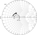
- FIG. 5 is an explanatory diagram for explaining the output results of the Smith chart at each position of the variable attenuator 10 of this embodiment.
- FIG. 5 shows the variable attenuator 10 of this embodiment shown in FIG. 1 in a state where the first switch 110 and the second switch 130 are turned on.
- an open stub 105 is connected to the center of the transmission line 100 between the input terminal P10 and the output terminal P11 of the variable attenuator 10.
- the output results of the Smith chart at multiple positions of the variable attenuator 10 are shown in FIG. 6 to FIG. 10, respectively.
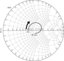
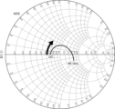
- FIG. 6 shows the output result of the Smith chart at position a of the variable attenuator 10 shown in FIG. 5.
- FIG. 7 shows the output result of the Smith chart at position b of the variable attenuator 10 shown in FIG. 5.
- FIG. 8 shows the output result of the Smith chart at position c of the variable attenuator 10 shown in FIG. 5.
- FIG. 9 shows the output result of the Smith chart at position d of the variable attenuator 10 shown in FIG. 5.
- FIG. 10 shows the output result of the Smith chart at position e of the variable attenuator 10 shown in FIG. 5.
- the Smith charts in FIG. 6 to FIG. 10 show the impedance distribution in the frequency range of 0 GHz (DC) to 90 GHz of the signal transmitted to the variable attenuator 10 with thick lines.
- the open stub 105 behaves as a shunt capacitor, so that the open stub 105 and the ⁇ /8 transmission line 100 arranged between the positions b and c can be combined to compensate for the reactance component at high frequencies (around 90 GHz in this case).
- the distribution near high frequencies in FIGS. 6 to 8 approaches the horizontal axis representing the resistance component.
- the open stub 105 moves the impedance of the circuit counterclockwise on the Smith chart, and the variable attenuator 10 of this embodiment can shorten the electrical length l series of the transmission line 100 between the input terminal P10 and the output terminal P11 to less than ⁇ /4, and then perform impedance conversion to the target impedance. Therefore, the electrical length of the transmission line 100 between the input terminal P10 and the output terminal P11 can be shortened, and the chip size can be reduced.
- the variable attenuator 500 of the reference example includes a transmission line 510, a fifth resistor 520, and a sixth resistor 530.
- the transmission line 510 has the same configuration as the transmission line 100 (particularly the straight line of the transmission line 100) between the input terminal P10 and the output terminal P11 of the variable attenuator 10 of FIG. 5, but does not have an open stub.
- the fifth resistor 520 is connected between the input terminal IN and the reference potential, and has the same configuration as the first resistor 120 of the variable attenuator 10 of FIG. 5.
- the sixth resistor 530 is connected between the output terminal OUT and the reference potential, and has the same configuration as the second resistor 140 of the variable attenuator 10 of FIG. 5.
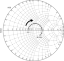
- the output results of the Smith chart at multiple positions of the variable attenuator 500 of the reference example are shown in FIG. 12 to FIG. 14, respectively.
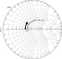
- FIG. 12 shows the output result of the Smith chart at position a of the variable attenuator 500 shown in FIG. 11.
- FIG. 13 shows the output result of the Smith chart at position b of the variable attenuator 500 shown in FIG. 11.
- FIG. 14 shows the output result of the Smith chart at position c of the variable attenuator 500 shown in FIG. 11.
- the Smith charts in FIG. 12 to FIG. 14 show the impedance distribution in the frequency range of the transmitted signal from 0 GHz (DC) to 90 GHz with thick lines.
- the impedance near high frequencies is distributed away from the horizontal axis on the Smith chart shown in FIG. 12 due to the transmission line 510. Therefore, the impedance near high frequencies cannot be brought close enough to the horizontal axis by the transmission line 510 alone, and impedance conversion to the target impedance is not possible.
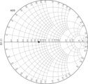
- Fig. 15 shows the relationship between the impedance and the length I stub of the open stub 105 as viewed from the connection position of the transmission line 100.
- the horizontal axis shows the length I stub of the open stub 105 from the connection position of the transmission line 100 between the input terminal P10 and the output terminal P11 in Fig. 1
- the vertical axis shows the impedance of the open stub 105 as viewed from the connection position of the transmission line 100.
- the open stub 105 in the range of the length of the open stub 105 being 0 ⁇ I stub ⁇ ⁇ /4 (particularly, ⁇ /8 ⁇ l stub ), the open stub 105 exhibits capacitive properties and operates as a shunt capacitor. Therefore, the electrical length of the open stub 105 in the variable attenuator 10 of this embodiment is preferably in the range of 0 ⁇ I stub ⁇ ⁇ /4, particularly ⁇ /8 ⁇ l stub .
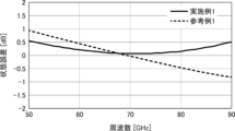
- FIG. 16 shows the results of simulating the state error of a variable attenuator 10 with an attenuation of 8 dB.
- the horizontal axis indicates the frequency of the transmitted signal, and the vertical axis indicates the state error (variation from the nominal value of the attenuation amount).
- Example 1 shows the results of simulating the state error of the variable attenuator 10 of the present embodiment in FIG. 2, and Reference Example 1 shows the results of simulating the state error of a variable attenuator that has the same configuration as the variable attenuator 10 of the present embodiment in FIG. 2 but does not have an open stub.
- the maximum state error in Example 1 is 0.5 dB, and the maximum state error in Reference Example 1 is 0.9 dB. It can be seen that by using the variable attenuator 10 of this embodiment, the state error is improved by 0.4 dB compared to Reference Example 1.
- a variable attenuator with an attenuation of 8 dB has a larger attenuation amount, so in Reference Example 1, it is necessary to widen the gate width of the shunt HEMT used as a switch from the viewpoint of allowable current and distortion characteristics.
- widening the gate width of the shunt HEMT increases the capacitance of the circuit, and impedance conversion (impedance matching) cannot be performed well for large capacitance, and the state error of the variable attenuator increases.
- the state error of the variable attenuator with an attenuation amount of 4 dB was a maximum of 0.4 dB
- the state error of the variable attenuator with an attenuation amount of 8 dB was a maximum of 0.9 dB.
- variable attenuator 10 of this embodiment impedance conversion is performed using the open stub 105, making it possible to reduce the state error even with a large attenuation amount.
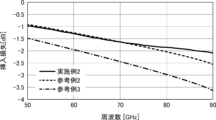
- FIG. 17 shows the results of a simulation of the insertion loss during thru (attenuation of 0 dB) of the step attenuators in Example 2, Reference Example 2, and Reference Example 3.
- the horizontal axis indicates the frequency of the signal to be transmitted, and the vertical axis indicates the insertion loss (dB).
- the step attenuator 300 of Example 2 is configured by cascading five variable attenuators 10 of the present embodiment shown in FIG. 2.
- the step attenuator 300 of Example 2 has an operating frequency of 50-90 GHz, includes one variable attenuator 10 with an attenuation of 4 dB, and three variable attenuators 10 with an attenuation of 8 dB, for a total attenuation of 28 dB.
- Each of the five variable attenuators 10 has an electrical length of ⁇ /4 between the input terminal P10 and the output terminal P11, and the first switch 110 and the second switch 130 are HEMTs.
- Reference Example 2 uses a step attenuator with the same configuration as step attenuator 300 of Example 2, except that each variable attenuator of the step attenuator of Reference Example 2 does not have an open stub.
- the step attenuator of Reference Example 3 is configured by cascading seven variable attenuators 10 of this embodiment shown in FIG. 2, except that each variable attenuator of the step attenuator of Reference Example 2 does not have an open stub.
- the step attenuator of Reference Example 3 has an operating frequency of 50-90 GHz, and includes seven variable attenuators with an attenuation of 4 dB, for a total attenuation of 28 dB.
- Each switch in the variable attenuators of Reference Examples 2 and 3 is a HEMT.
- each variable attenuator in Reference Example 3 the gate width of the shunt HEMT used in each variable attenuator is smaller, so the capacitive effect of the switches is smaller, but the number of cascaded variable attenuators required to achieve the desired attenuation of 28 dB is greater than in Reference Example 2. If the insertion loss of each variable attenuator in Reference Example 3 during thru (attenuation of 0 dB) is just over 0.5 dB, cascading seven stages will result in the insertion loss of the entire step attenuator being just over 3.5 dB. In Example 2, the insertion loss during thru (attenuation of 0 dB) is significantly improved by 1.4 dB compared to Reference Example 3, which has a larger number of cascaded connections.
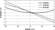
- FIG. 18 shows the results of simulating the state error of the step attenuator in Example 2, Reference Example 2, and Reference Example 3.
- the horizontal axis indicates the frequency of the transmitted signal, and the vertical axis indicates the state error (dB).
- Example 2, Reference Example 2, and Reference Example 3 in FIG. 18 are step attenuators with the same configuration as the simulation in FIG. 17.
- Example 2 a variable attenuator with an attenuation of 8 dB is used, so the state error is larger than in Reference Example 3, and the state error shown in Figure 16 is further increased by the cascade connection. In Example 2, the state error is improved compared to Reference Examples 2 and 3.
- the length of the transmission line between the input terminal and output terminal of the variable attenuator is 300 um for the variable attenuator with an attenuation of 4 dB in Reference Example 2 and 320 um for the variable attenuator with an attenuation of 8 dB in Example 2, whereas it is 255 um for the variable attenuator 10 with an attenuation of 4 dB and 270 um for the variable attenuator 10 with an attenuation of 8 dB in Example 2. Therefore, by using the step attenuator in Example 2, the chip size is approximately 15% smaller than the step attenuator in Reference Example 2. Note that the open stub 105 in Example 2 is sufficiently shorter in length than the shunt HEMT and resistor, and does not contribute to an increase in chip size.
- variable attenuator 10 of this embodiment allows impedance adjustment using the transmission line 100 with the open stub 105, so insertion loss during thru (attenuation amount 0 dB) can be reduced, and state errors can also be reduced. Furthermore, the variable attenuator 10 of this embodiment allows a design that shortens the transmission line 100 between the input terminal P10 and the output terminal P11, reducing the chip size and contributing to high-density implementation of the RF test front end.
Landscapes
- Non-Reversible Transmitting Devices (AREA)
- Attenuators (AREA)
- Transmitters (AREA)
Abstract
La présente invention concerne un atténuateur variable comprenant : une ligne de transmission ayant un tronçon ouvert connecté entre une entrée et une sortie de l'atténuateur variable ; un premier commutateur connecté entre l'entrée et un potentiel de référence ; et un second commutateur connecté entre la sortie et le potentiel de référence.
Priority Applications (3)
| Application Number | Priority Date | Filing Date | Title |
|---|---|---|---|
| PCT/JP2023/030182 WO2025041272A1 (fr) | 2023-08-22 | 2023-08-22 | Atténuateur variable, atténuateur à plots et dispositif de test |
| CN202380101359.5A CN121693858A (zh) | 2023-08-22 | 2023-08-22 | 可变衰减器、步进衰减器及试验装置 |
| TW113119661A TW202510401A (zh) | 2023-08-22 | 2024-05-28 | 可變衰減器、步進衰減器及試驗裝置 |
Applications Claiming Priority (1)
| Application Number | Priority Date | Filing Date | Title |
|---|---|---|---|
| PCT/JP2023/030182 WO2025041272A1 (fr) | 2023-08-22 | 2023-08-22 | Atténuateur variable, atténuateur à plots et dispositif de test |
Publications (1)
| Publication Number | Publication Date |
|---|---|
| WO2025041272A1 true WO2025041272A1 (fr) | 2025-02-27 |
Family
ID=94731982
Family Applications (1)
| Application Number | Title | Priority Date | Filing Date |
|---|---|---|---|
| PCT/JP2023/030182 Pending WO2025041272A1 (fr) | 2023-08-22 | 2023-08-22 | Atténuateur variable, atténuateur à plots et dispositif de test |
Country Status (3)
| Country | Link |
|---|---|
| CN (1) | CN121693858A (fr) |
| TW (1) | TW202510401A (fr) |
| WO (1) | WO2025041272A1 (fr) |
Citations (5)
| Publication number | Priority date | Publication date | Assignee | Title |
|---|---|---|---|---|
| JP2011234110A (ja) * | 2010-04-27 | 2011-11-17 | Mitsubishi Electric Corp | 高周波回路 |
| JP2012015613A (ja) * | 2010-06-29 | 2012-01-19 | Advantest Corp | ステップ減衰装置およびそれを用いた試験装置および信号発生器 |
| US20120208484A1 (en) * | 2009-08-18 | 2012-08-16 | Kyle David Holzer | Optimized automated test equipment multi-path receiver concept |
| JP2014002051A (ja) * | 2012-06-19 | 2014-01-09 | Advantest Corp | 試験装置 |
| US20180234080A1 (en) * | 2017-02-15 | 2018-08-16 | Psemi Corporation | Self-matching phase shifter/attenuator |
-
2023
- 2023-08-22 WO PCT/JP2023/030182 patent/WO2025041272A1/fr active Pending
- 2023-08-22 CN CN202380101359.5A patent/CN121693858A/zh active Pending
-
2024
- 2024-05-28 TW TW113119661A patent/TW202510401A/zh unknown
Patent Citations (5)
| Publication number | Priority date | Publication date | Assignee | Title |
|---|---|---|---|---|
| US20120208484A1 (en) * | 2009-08-18 | 2012-08-16 | Kyle David Holzer | Optimized automated test equipment multi-path receiver concept |
| JP2011234110A (ja) * | 2010-04-27 | 2011-11-17 | Mitsubishi Electric Corp | 高周波回路 |
| JP2012015613A (ja) * | 2010-06-29 | 2012-01-19 | Advantest Corp | ステップ減衰装置およびそれを用いた試験装置および信号発生器 |
| JP2014002051A (ja) * | 2012-06-19 | 2014-01-09 | Advantest Corp | 試験装置 |
| US20180234080A1 (en) * | 2017-02-15 | 2018-08-16 | Psemi Corporation | Self-matching phase shifter/attenuator |
Also Published As
| Publication number | Publication date |
|---|---|
| CN121693858A (zh) | 2026-03-17 |
| TW202510401A (zh) | 2025-03-01 |
Similar Documents
| Publication | Publication Date | Title |
|---|---|---|
| CN107210713B (zh) | 多尔蒂放大器 | |
| US6737933B2 (en) | Circuit topology for attenuator and switch circuits | |
| US7508267B1 (en) | GaN based digital controlled broadband MMIC power amplifier | |
| CN104393389A (zh) | 一种具有幅度和相位补偿功能的宽带移相功分器 | |
| JP2019134404A (ja) | 負荷変調アンプ | |
| Gonçalves et al. | Switch-based variable length stubs network for PA load sensitivity reduction | |
| EP3096453A1 (fr) | Coupleur de degré 0/90 avec terminaison complexe | |
| Akbarpour et al. | Analytical design methodology for generic Doherty amplifier architectures using three-port input/output networks | |
| CN118232884A (zh) | 基于mmic的延时线结构、延时芯片及相控阵雷达系统 | |
| WO2025041272A1 (fr) | Atténuateur variable, atténuateur à plots et dispositif de test | |
| CN112350671A (zh) | 使用宽带增益均衡器的延迟补偿 | |
| EP3297157B1 (fr) | Procédé de conception pour amplificateur à trajets multiples et amplificateur à trajets multiples | |
| US20060244548A1 (en) | Attenuator system | |
| Zaid et al. | 16 Watt S-band GaN based power amplifier using replicating stages | |
| CN114337710B (zh) | 一种用于射频信号接收的增益切换电路和射频接收器 | |
| KR102755329B1 (ko) | 트랜스포머 기반 증폭기, 이의 동작 방법, 및 이를 포함하는 장치들 | |
| CN114123995A (zh) | 一种新型的并发双波段射频功率放大器 | |
| Sah et al. | Prototype for an optimized drive signal control system for a 2.5 GHz Doherty power amplifier | |
| Tekin et al. | Compact wide-band gysel power divider | |
| US12483196B2 (en) | Multiple-mode RF power amplifiers | |
| Paul et al. | A new approach for the linearization of a distributed amplifier | |
| CN120825195B (zh) | 一种射频电路和电子设备 | |
| Nazari et al. | Design of a wideband low noise amplifier using modified cascode structure for 45GHz band applications | |
| Li et al. | High-Linearity RF Canceller With Precision Control for L-Band Full-Duplex Transceivers | |
| Hu et al. | Concurrent tri-band power amplifier based on novel tri-band impedance transformer |
Legal Events
| Date | Code | Title | Description |
|---|---|---|---|
| 121 | Ep: the epo has been informed by wipo that ep was designated in this application |
Ref document number: 23949733 Country of ref document: EP Kind code of ref document: A1 |
|
| NENP | Non-entry into the national phase |
Ref country code: DE |