WO2025041255A1 - Dispositif d'affichage - Google Patents
Dispositif d'affichage Download PDFInfo
- Publication number
- WO2025041255A1 WO2025041255A1 PCT/JP2023/030117 JP2023030117W WO2025041255A1 WO 2025041255 A1 WO2025041255 A1 WO 2025041255A1 JP 2023030117 W JP2023030117 W JP 2023030117W WO 2025041255 A1 WO2025041255 A1 WO 2025041255A1
- Authority
- WO
- WIPO (PCT)
- Prior art keywords
- support substrate
- region
- display device
- fixing
- free
- Prior art date
- Legal status (The legal status is an assumption and is not a legal conclusion. Google has not performed a legal analysis and makes no representation as to the accuracy of the status listed.)
- Pending
Links
Images


Classifications
-
- G—PHYSICS
- G09—EDUCATION; CRYPTOGRAPHY; DISPLAY; ADVERTISING; SEALS
- G09F—DISPLAYING; ADVERTISING; SIGNS; LABELS OR NAME-PLATES; SEALS
- G09F9/00—Indicating arrangements for variable information in which the information is built-up on a support by selection or combination of individual elements
- G09F9/30—Indicating arrangements for variable information in which the information is built-up on a support by selection or combination of individual elements in which the desired character or characters are formed by combining individual elements
-
- H—ELECTRICITY
- H05—ELECTRIC TECHNIQUES NOT OTHERWISE PROVIDED FOR
- H05B—ELECTRIC HEATING; ELECTRIC LIGHT SOURCES NOT OTHERWISE PROVIDED FOR; CIRCUIT ARRANGEMENTS FOR ELECTRIC LIGHT SOURCES, IN GENERAL
- H05B33/00—Electroluminescent light sources
- H05B33/02—Details
-
- H—ELECTRICITY
- H05—ELECTRIC TECHNIQUES NOT OTHERWISE PROVIDED FOR
- H05B—ELECTRIC HEATING; ELECTRIC LIGHT SOURCES NOT OTHERWISE PROVIDED FOR; CIRCUIT ARRANGEMENTS FOR ELECTRIC LIGHT SOURCES, IN GENERAL
- H05B33/00—Electroluminescent light sources
- H05B33/12—Light sources with substantially two-dimensional [2D] radiating surfaces
- H05B33/14—Light sources with substantially two-dimensional [2D] radiating surfaces characterised by the chemical or physical composition or the arrangement of the electroluminescent material, or by the simultaneous addition of the electroluminescent material in or onto the light source
-
- H—ELECTRICITY
- H10—SEMICONDUCTOR DEVICES; ELECTRIC SOLID-STATE DEVICES NOT OTHERWISE PROVIDED FOR
- H10K—ORGANIC ELECTRIC SOLID-STATE DEVICES
- H10K50/00—Organic light-emitting devices
- H10K50/10—OLEDs or polymer light-emitting diodes [PLED]
-
- H—ELECTRICITY
- H10—SEMICONDUCTOR DEVICES; ELECTRIC SOLID-STATE DEVICES NOT OTHERWISE PROVIDED FOR
- H10K—ORGANIC ELECTRIC SOLID-STATE DEVICES
- H10K50/00—Organic light-emitting devices
- H10K50/10—OLEDs or polymer light-emitting diodes [PLED]
- H10K50/11—OLEDs or polymer light-emitting diodes [PLED] characterised by the electroluminescent [EL] layers
- H10K50/115—OLEDs or polymer light-emitting diodes [PLED] characterised by the electroluminescent [EL] layers comprising active inorganic nanostructures, e.g. luminescent quantum dots
-
- H—ELECTRICITY
- H10—SEMICONDUCTOR DEVICES; ELECTRIC SOLID-STATE DEVICES NOT OTHERWISE PROVIDED FOR
- H10K—ORGANIC ELECTRIC SOLID-STATE DEVICES
- H10K59/00—Integrated devices, or assemblies of multiple devices, comprising at least one organic light-emitting element covered by group H10K50/00
- H10K59/90—Assemblies of multiple devices comprising at least one organic light-emitting element
-
- H—ELECTRICITY
- H10—SEMICONDUCTOR DEVICES; ELECTRIC SOLID-STATE DEVICES NOT OTHERWISE PROVIDED FOR
- H10K—ORGANIC ELECTRIC SOLID-STATE DEVICES
- H10K77/00—Constructional details of devices covered by this subclass and not covered by groups H10K10/80, H10K30/80, H10K50/80 or H10K59/80
- H10K77/10—Substrates, e.g. flexible substrates
Definitions
- a display device is a foldable display device that includes a first support substrate, a second support substrate, and a flexible display panel and can be in an open state or a closed state, and the display panel has a bending region, a first fixing region fixed to the first support substrate, a second fixing region fixed to the second support substrate, a first free region located between the bending region and the first fixing region and not fixed to the first support substrate, and a second free region located between the bending region and the second fixing region and not fixed to the second support substrate.
- the configuration disclosed herein can reduce the occurrence of peeling inside the display device.
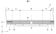
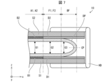
- 1 is a cross-sectional view showing an example of a configuration of a display device according to an embodiment of the present disclosure in a closed state.
- 1 is a cross-sectional view showing an example of a configuration of a display device according to an embodiment of the present disclosure in a closed state.
- 1 is a cross-sectional view showing an example of a configuration of a display device according to an embodiment of the present disclosure in an open state.
- 1 is a cross-sectional view showing an example of a configuration of a display device according to an embodiment of the present disclosure in a closed state.
- 11 is a plan view showing an example of the configuration of the flexible substrate shown in FIG. 9 and FIG. 10.
- 1 is a cross-sectional view showing a modified example of the configuration of a display device according to an embodiment of the present disclosure in an open state.
- 1 is a cross-sectional view showing a modified example of the configuration of a display device according to an embodiment of the present disclosure in an open state.
- 1 is a cross-sectional view showing a modified example of the configuration of a display device according to an embodiment of the present disclosure in an open state.
- 1 is a cross-sectional view showing an example of a configuration of a display device according to an embodiment of the present disclosure in an open state.
- 10 is a cross-sectional view showing a modified example of the configuration of the display device according to Comparative Example 1 in an open state.
- FIG. 10 is a cross-sectional view showing a modified example of the configuration of the display device according to Comparative Example 1 in an open state.
- FIG. 13 is a graph showing the results of a simulation of compressive stress and tensile stress generated in a display panel in a closed state.
- 13 is a diagram showing a simulation result of compressive stress and tensile stress generated in a display panel according to Comparative Example 1 in a closed state, superimposed on a cross-sectional view.
- FIG. 11 is a diagram showing a simulation result of compressive stress and tensile stress generated in the display panel according to Example 1 in a closed state, superimposed on a cross-sectional view.
- FIG. 13 is a graph showing the results of a simulation of compressive stress and tensile stress generated in a display panel in a closed state.
- 13 is a diagram showing a simulation result of compressive stress and tensile stress generated in a display panel according to Comparative Example 1 in a closed state, superimposed on
- FIG. 1 is a cross-sectional view showing an example of the configuration of a display device according to an embodiment of the present disclosure in an open state.
- FIG. 2 is a cross-sectional view showing an example of the configuration of a display device according to an embodiment of the present disclosure in a closed state.
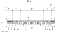
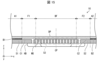
- a display device 10 according to an embodiment of the present disclosure is a foldable display device that includes a first support substrate S1, a second support substrate S2, and a flexible display panel DP and can be in an open state and a closed state.
- the display panel DP has a bending region BF, a first fixing region A1 fixed to the first support substrate S1, a second fixing region A2 fixed to the second support substrate S2, a first free region F1 located between the bending region BF and the first fixing region A1 and not fixed to the first support substrate S1, and a second free region F2 located between the bending region BF and the second fixing region A2 and not fixed to the second support substrate S2.
- the direction in which the display panel DP is located relative to the first support substrate S1 is defined as the z direction
- the direction in which the second support substrate S2 is located relative to the first support substrate S1 in the open state is defined as the x direction
- the direction perpendicular to the x direction and z direction is defined as the y direction.
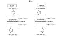
- FIG. 3 is a diagram showing external forces and internal stresses in the bonding direction according to the present disclosure.
- a tensile force when a tensile force is applied to the display panel, a tensile stress acts to peel objects 1 and 2 from the bonding surface.
- a compressive force when a compressive force is applied to the display panel, a compressive stress acts to press objects 1 and 2 against the bonding surface.
- the tensile force and tensile stress shown on the left side of FIG. 3 are in the positive direction, and the compressive force and compressive stress shown on the right side of FIG. 3 are in the negative direction.
- FIG. 4 is a diagram showing external forces and internal stresses in the shear direction according to the present disclosure.
- a shear stress acts that tends to displace object 1 and object 2 from the joint surface.
- the force in the shear direction and the shear stress shown on the left side of FIG. 4 are positive directions, and the force in the shear direction and the shear stress shown on the right side of FIG. 4 are negative directions.
- peeling stress when the tensile stress and shear stress acting on the bonding surface exceed the bonding strength, object 1 and object 2 peel off from the bonding surface.
- peeling stress the tensile stress and shear stress that can cause peeling are collectively referred to as "peeling stress.” Note that the simulations described below (see Figures 18 to 23) are not actual experiments but numerical experiments on a computer. For simplification, in the stress simulations (see Figures 18 to 22), a model in which peeling does not occur was used, i.e., a model in which the bonding strength of the bonding surface is infinite.
- the configuration according to the present disclosure can reduce the occurrence of peeling inside the display device 10 compared to a configuration in which there is no free region between the fixed region and the bent region.
- the widths of the first free region F1 and the second free region F2 may each be 1 to 20 mm.
- “width” refers to the size in the x direction in the open state unless otherwise specified.
- the bending region BF is located between the first free region F1 and the second free region F2, and is continuously connected to the first free region F1 and the second free region F2.
- the first free region F1 is continuously connected to the first fixed region A1
- the second free region F2 is continuously connected to the second fixed region A2.
- the first fixed region A1 and the first free region F1 are located on the same plane as each other, and the second free region F2 and the second fixed region A2 are located on the same plane as each other.
- the display panel DP includes a cushion material BA as a layer closest to the first support substrate S1 and the second support substrate S2.
- the display panel DP includes a cushion material BA bonded to the flexible substrate 1 via an adhesive layer M1, and the cushion material BA is fixed to the first support substrate S1 and the second support substrate S2 via a first fixing material B1 and a second fixing material B2.
- the first support substrate S1 and the second support substrate S2 are each a metal plate, a resin plate, or a fiber-reinforced resin plate.
- the fiber-reinforced resin plate includes a carbon plate containing carbon fiber.
- the first support substrate S1 and the second support substrate S2 may be mechanically connected to each other in a movable manner by a hinge device HD.
- a first end of the hinge device HD may be directly or indirectly fixed to the first support substrate S1, and a second end of the hinge device HD may be directly or indirectly fixed to the second support substrate S2.
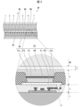
- the display panel DP can have a light-emitting element ED including an organic light-emitting layer or a quantum dot light-emitting layer as an emission layer EM.
- the display panel DP includes a flexible substrate 1, a transistor layer 2 including circuit elements such as transistors Tr and wiring, a display layer 3 including the light-emitting element ED, and a sealing layer 4 for preventing oxygen and moisture from entering the light-emitting element ED.
- the light-emitting element ED may have an anode E1 and a cathode E2, and an emission layer EM located between the anode E1 and the cathode E2.
- the light-emitting element ED may further have an electron injection layer EIL and an electron transport layer ETL for facilitating the injection of electrons into the emission layer EM, and a hole injection layer HIL and a hole transport layer HTL for facilitating the injection of holes into the emission layer EM.
- the display panel DP may include, above the sealing layer 4, an adhesive layer M2, a touch panel layer 5, an adhesive layer M3, a polarizing film 6, an adhesive layer M4, and a flexible cover 7, in this order.
- the quantum dots are semiconductor particles having a particle size of, for example, 100 nm or less, and may have II-VI group semiconductor compounds such as MgS, MgSe, MgTe, CaS, CaSe, CaTe, SrS, SrSe, SrTe, BaS, BaSe, BaTe, ZnS, ZnSe, ZnTe, CdS, CdSe, CdTe, HgS, HgSe, HgTe, and/or crystals of III-V group semiconductor compounds such as GaAs, GaP, InN, InAs, InP, InSb, and/or crystals of IV group semiconductor compounds such as Si and Ge.
- II-VI group semiconductor compounds such as MgS, MgSe, MgTe, CaS, CaSe, CaTe, SrS, SrSe, SrTe, BaS, BaSe, BaTe, ZnS, ZnSe, ZnTe, CdS
- the cushioning material BA may include multiple layers and may include an adhesive layer.
- Materials included in the cushioning material BA include polyethylene terephthalate (PET) resins, acrylic resins, urethane resins, polyester resins, stainless steel, aluminum, titanium, copper, etc.
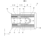
- FIG. 7 is a cross-sectional view showing an example of the configuration of a display device according to an embodiment of the present disclosure in a closed state.
- the display device 10 may have a first step adjustment material D1 adjacent to the first fixing material B1 and located between the first support substrate S1 and the first free area F1 of the display panel DP, and a second step adjustment material D2 adjacent to the second fixing material B2 and located between the second support substrate S2 and the second free area F2 of the display panel DP.
- the first fixing material B1 and the first step adjustment material D1 may be in contact with each other, and the second fixing material B2 and the second step adjustment material D2 may be in contact with each other.
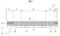
- Fig. 9 is a cross-sectional view showing an example of the configuration of a display device according to an embodiment of the present disclosure in an open state.
- Fig. 10 is a cross-sectional view showing an example of the configuration of a display device according to an embodiment of the present disclosure in a closed state.
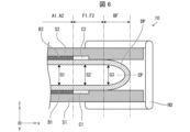
- the display device 10 may include a flexible substrate S3 that is continuously connected to the first support substrate S1 and the second support substrate S2 and is integrated with the first support substrate S1 and the second support substrate S2.
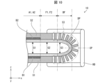
- FIG. 11 is a plan view showing an example of the configuration of the flexible substrate shown in FIGS. 9 and 10.
- the flexible substrate S3 may be a portion that has been shaped to reduce the second moment of area of the rigid substrate S4, and each of the first support substrate S1 and the second support substrate S2 may be a portion that has not been shaped to reduce the second moment of area of the rigid substrate S4.
- the shaping process that reduces the second moment of area of the portion of the rigid substrate S4 includes processing to form an opening K in that portion. Therefore, the flexible substrate S3 may include one or more openings K.
- the openings K may or may not penetrate all the way through.
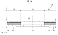
- FIG. 16 is a cross-sectional view showing the configuration of the display device according to Comparative Example 1 in an open state.
- the display device 100 according to Comparative Example 1 was a foldable display device that had a first support substrate 101, a second support substrate 102, and a flexible display panel 103, and could be in an open state or a closed state.
- the display panel 103 had a bending region 110, a first fixing region 111 fixed to the first support substrate 101 by a first fixing member 104, and a second fixing region 112 fixed to the second support substrate 102 by a second fixing member 105.
- the bending region 110 was directly connected to the first fixing region 111 and the second fixing region 112.
- the width of the bending region 110 according to Comparative Example 1 was approximately the same as the width of the bending region BF according to Example 1 of the present disclosure.
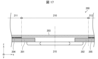
- FIG. 17 is a cross-sectional view showing the configuration of a display device according to Comparative Example 2 in an open state.
- the display device 200 according to Comparative Example 1 was a folding display device that had a first support substrate 201, a second support substrate 202, and a flexible display panel 203, and could be in an open state or a closed state.
- the display panel 203 had a bending region 210, a first fixing region 211 fixed to the first support substrate 201 by a first fixing member 204, and a second fixing region 212 fixed to the second support substrate 202 by a second fixing member 205.
- the bending region 210 was continuously connected to the first fixing region 211 and the second fixing region 212.
- the width of the bending region 210 according to Comparative Example 2 was the same as the total width of the first free region F1, the bending region BF, and the second free region F2 according to Example 1 of the present disclosure.
- Example 1 Comparative Example 1, and Comparative Example 2, the display panel DP, 103, 203 was flat in the open state, and the distance of the gap G1 between the first fixing area A1, 111, 211 and the second fixing area A2, 112, 212 in the closed state was 3.0 mm.
- FIG. 18 is a graph showing the results of a simulation of compressive stress and tensile stress occurring in the display panel in the closed state. On the vertical axis, positive indicates compressive stress and negative indicates tensile stress. As shown in FIG. 18, the graphs of Comparative Example 1 and Example 1 almost overlap, and the peak value of the tensile stress in Comparative Example 1 is 0.43 times that of Comparative Example 2, and in Example 1 it is 0.42 times that of Comparative Example 2. Peeling usually occurs between layers with the weakest adhesive strength. Typically, the adhesive strength between the display panel DP and the first and second support substrates S1, S2 is stronger than the adhesive strength inside the display panel DP, and peeling tends to occur inside the display panel DP. Therefore, compared to the display panel 203 of Comparative Example 2, peeling is less likely to occur inside the display panel DP in Example 1.
- the distance from the bending center CP in Example 1 to the boundary between the bending region BF and the first free region F1 was 2.4 mm to 3.2 mm.
- the distance from the bending center 115 in Comparative Example 1 to the boundary between the bending region 110 and the first fixed region 111 in Comparative Example 1 was 2.4 mm to 3.2 mm.
- the distance from the bending center 215 in Comparative Example 2 to the boundary between the bending region 210 and the first fixed region 211 was 4.8 mm to 6.2 mm.
- the peak positions of the tensile stress were in the first and second fixed regions 111, 112, 211, 212 in Comparative Examples 1 and 2, and in Example 1, they were in the first and second free regions F1, F2. Therefore, in the actual experiment, it is expected that the display panel DP will be less likely to peel off from the first and second support substrates S1, S2 in Example 1 compared to Comparative Examples 1 and 2.
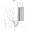
- FIG. 19 is a diagram showing the results of a simulation of compressive stress and tensile stress occurring in the display panel of Comparative Example 1 in the closed state superimposed on a cross-sectional view.
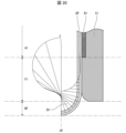
- FIG. 20 is a diagram showing the results of a simulation of compressive stress and tensile stress occurring in the display panel of Example 1 in the closed state superimposed on a cross-sectional view.
- the length of a line segment extending from the central surface of display panel 103, DP indicates the magnitude of tensile stress or compressive stress.
- the support substrate side relative to the central surface of display panel 103, DP indicates tensile stress, and the side opposite the support substrate indicates compressive stress.
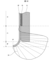
- FIG. 21 is a diagram showing the results of a simulation of the shear stress generated in the display panel of Comparative Example 1 in the closed state superimposed on a cross-sectional view.
- FIG. 22 is a diagram showing the results of a simulation of the shear stress generated in the display panel of Example 1 in the closed state superimposed on a cross-sectional view.
- the length of the line extending from the central surface of the display panel 103, DP indicates the magnitude of the shear stress.
- the support substrate side of the central surface of the display panel 103, DP indicates negative shear stress, and the side opposite the support substrate indicates positive shear stress. Note that in this simulation, the direction from the center of bending toward the edge of the display panel was considered positive, and the opposite direction was considered negative.
- FIG. 23 is a cross-sectional view showing the results of a simulation of the deformation and movement of the display panel in Example 1 in the closed state.
- Example 1 the display panel DP floated up from the first support substrate S1 in range R. Note that the distance of the float was very small.
Landscapes
- Physics & Mathematics (AREA)
- Optics & Photonics (AREA)
- Engineering & Computer Science (AREA)
- Chemical & Material Sciences (AREA)
- Crystallography & Structural Chemistry (AREA)
- Inorganic Chemistry (AREA)
- Nanotechnology (AREA)
- General Physics & Mathematics (AREA)
- Theoretical Computer Science (AREA)
- Electroluminescent Light Sources (AREA)
- Devices For Indicating Variable Information By Combining Individual Elements (AREA)
Abstract
Un dispositif d'affichage selon la présente divulgation comprend un panneau d'affichage (DP) flexible comprenant : une région de flexion (BF) ; une première région fixe (A1) fixée à un premier substrat de support (S1) ; une seconde région fixe (A2) fixée à un second substrat de support (S2) ; une première région libre (F1) située entre la région de flexion (BF) et la première région fixe (A1) et non fixée au premier substrat de support (S1) ; et une seconde région libre (F2) située entre la région de flexion (BF) et la seconde région fixe (A2) et non fixée au second substrat de support (S2).
Priority Applications (1)
| Application Number | Priority Date | Filing Date | Title |
|---|---|---|---|
| PCT/JP2023/030117 WO2025041255A1 (fr) | 2023-08-22 | 2023-08-22 | Dispositif d'affichage |
Applications Claiming Priority (1)
| Application Number | Priority Date | Filing Date | Title |
|---|---|---|---|
| PCT/JP2023/030117 WO2025041255A1 (fr) | 2023-08-22 | 2023-08-22 | Dispositif d'affichage |
Publications (1)
| Publication Number | Publication Date |
|---|---|
| WO2025041255A1 true WO2025041255A1 (fr) | 2025-02-27 |
Family
ID=94731939
Family Applications (1)
| Application Number | Title | Priority Date | Filing Date |
|---|---|---|---|
| PCT/JP2023/030117 Pending WO2025041255A1 (fr) | 2023-08-22 | 2023-08-22 | Dispositif d'affichage |
Country Status (1)
| Country | Link |
|---|---|
| WO (1) | WO2025041255A1 (fr) |
Citations (2)
| Publication number | Priority date | Publication date | Assignee | Title |
|---|---|---|---|---|
| US20200319672A1 (en) * | 2019-03-11 | 2020-10-08 | Samsung Electronics Co., Ltd. | Electronic device including foldable conductive plate |
| CN115311942A (zh) * | 2022-07-22 | 2022-11-08 | 昆山国显光电有限公司 | 显示模组及显示装置 |
-
2023
- 2023-08-22 WO PCT/JP2023/030117 patent/WO2025041255A1/fr active Pending
Patent Citations (2)
| Publication number | Priority date | Publication date | Assignee | Title |
|---|---|---|---|---|
| US20200319672A1 (en) * | 2019-03-11 | 2020-10-08 | Samsung Electronics Co., Ltd. | Electronic device including foldable conductive plate |
| CN115311942A (zh) * | 2022-07-22 | 2022-11-08 | 昆山国显光电有限公司 | 显示模组及显示装置 |
Similar Documents
| Publication | Publication Date | Title |
|---|---|---|
| CN100380574C (zh) | 剥离方法及半导体器件的制造方法 | |
| CN108987434B (zh) | 电致发光设备、柔性显示装置及其制造方法 | |
| CN111976249B (zh) | 复合泡棉层以及显示模组 | |
| US11175764B2 (en) | Touch display device | |
| US20230229196A1 (en) | Display module and display device | |
| US11462699B2 (en) | Display panel, method for manufacturing the same and display device | |
| JP7237005B2 (ja) | 表示基板、表示装置、表示基板の製造方法 | |
| EP3498880A1 (fr) | Plaque de masquage et dispositif d'évaporation | |
| CN113284423B (zh) | 一种柔性显示面板及显示装置 | |
| JP2018170426A (ja) | 発光装置 | |
| CN109728195B (zh) | 显示面板以及显示装置 | |
| US11793037B2 (en) | Display panel and display device | |
| CN111653205B (zh) | 可拉伸显示面板和显示装置 | |
| WO2025041255A1 (fr) | Dispositif d'affichage | |
| US20200119110A1 (en) | Flexible organic light emitting diode display device and method of fabricating same | |
| WO2023087335A1 (fr) | Panneau d'affichage et procédé de préparation s'y rapportant | |
| US12057034B2 (en) | Display device | |
| US20250349230A1 (en) | Elastic member | |
| CN108550554A (zh) | 显示面板和显示装置 | |
| CN111162203A (zh) | 背膜及其制备方法、柔性显示装置及其制备方法、刀模 | |
| US7911138B2 (en) | Encapsulation cap and display device including the same | |
| US11744140B2 (en) | Flexible display panel and fabrication method thereof | |
| WO2026044916A1 (fr) | Module d'affichage et dispositif d'affichage | |
| DE102016125938A1 (de) | Flexibles, optoelektronisches Bauelement und Verfahren zum Herstellen des flexiblen, optoelektronischen Bauelements | |
| TW202315495A (zh) | 電子裝置及包含其的製備方法 |
Legal Events
| Date | Code | Title | Description |
|---|---|---|---|
| 121 | Ep: the epo has been informed by wipo that ep was designated in this application |
Ref document number: 23949716 Country of ref document: EP Kind code of ref document: A1 |
|
| NENP | Non-entry into the national phase |
Ref country code: DE |