WO2025041255A1 - Display device - Google Patents
Display device Download PDFInfo
- Publication number
- WO2025041255A1 WO2025041255A1 PCT/JP2023/030117 JP2023030117W WO2025041255A1 WO 2025041255 A1 WO2025041255 A1 WO 2025041255A1 JP 2023030117 W JP2023030117 W JP 2023030117W WO 2025041255 A1 WO2025041255 A1 WO 2025041255A1
- Authority
- WO
- WIPO (PCT)
- Prior art keywords
- support substrate
- region
- display device
- fixing
- free
- Prior art date
- Legal status (The legal status is an assumption and is not a legal conclusion. Google has not performed a legal analysis and makes no representation as to the accuracy of the status listed.)
- Pending
Links
Images


Classifications
-
- G—PHYSICS
- G09—EDUCATION; CRYPTOGRAPHY; DISPLAY; ADVERTISING; SEALS
- G09F—DISPLAYING; ADVERTISING; SIGNS; LABELS OR NAME-PLATES; SEALS
- G09F9/00—Indicating arrangements for variable information in which the information is built-up on a support by selection or combination of individual elements
- G09F9/30—Indicating arrangements for variable information in which the information is built-up on a support by selection or combination of individual elements in which the desired character or characters are formed by combining individual elements
-
- H—ELECTRICITY
- H05—ELECTRIC TECHNIQUES NOT OTHERWISE PROVIDED FOR
- H05B—ELECTRIC HEATING; ELECTRIC LIGHT SOURCES NOT OTHERWISE PROVIDED FOR; CIRCUIT ARRANGEMENTS FOR ELECTRIC LIGHT SOURCES, IN GENERAL
- H05B33/00—Electroluminescent light sources
- H05B33/02—Details
-
- H—ELECTRICITY
- H05—ELECTRIC TECHNIQUES NOT OTHERWISE PROVIDED FOR
- H05B—ELECTRIC HEATING; ELECTRIC LIGHT SOURCES NOT OTHERWISE PROVIDED FOR; CIRCUIT ARRANGEMENTS FOR ELECTRIC LIGHT SOURCES, IN GENERAL
- H05B33/00—Electroluminescent light sources
- H05B33/12—Light sources with substantially two-dimensional [2D] radiating surfaces
- H05B33/14—Light sources with substantially two-dimensional [2D] radiating surfaces characterised by the chemical or physical composition or the arrangement of the electroluminescent material, or by the simultaneous addition of the electroluminescent material in or onto the light source
-
- H—ELECTRICITY
- H10—SEMICONDUCTOR DEVICES; ELECTRIC SOLID-STATE DEVICES NOT OTHERWISE PROVIDED FOR
- H10K—ORGANIC ELECTRIC SOLID-STATE DEVICES
- H10K50/00—Organic light-emitting devices
- H10K50/10—OLEDs or polymer light-emitting diodes [PLED]
-
- H—ELECTRICITY
- H10—SEMICONDUCTOR DEVICES; ELECTRIC SOLID-STATE DEVICES NOT OTHERWISE PROVIDED FOR
- H10K—ORGANIC ELECTRIC SOLID-STATE DEVICES
- H10K50/00—Organic light-emitting devices
- H10K50/10—OLEDs or polymer light-emitting diodes [PLED]
- H10K50/11—OLEDs or polymer light-emitting diodes [PLED] characterised by the electroluminescent [EL] layers
- H10K50/115—OLEDs or polymer light-emitting diodes [PLED] characterised by the electroluminescent [EL] layers comprising active inorganic nanostructures, e.g. luminescent quantum dots
-
- H—ELECTRICITY
- H10—SEMICONDUCTOR DEVICES; ELECTRIC SOLID-STATE DEVICES NOT OTHERWISE PROVIDED FOR
- H10K—ORGANIC ELECTRIC SOLID-STATE DEVICES
- H10K59/00—Integrated devices, or assemblies of multiple devices, comprising at least one organic light-emitting element covered by group H10K50/00
- H10K59/90—Assemblies of multiple devices comprising at least one organic light-emitting element
-
- H—ELECTRICITY
- H10—SEMICONDUCTOR DEVICES; ELECTRIC SOLID-STATE DEVICES NOT OTHERWISE PROVIDED FOR
- H10K—ORGANIC ELECTRIC SOLID-STATE DEVICES
- H10K77/00—Constructional details of devices covered by this subclass and not covered by groups H10K10/80, H10K30/80, H10K50/80 or H10K59/80
- H10K77/10—Substrates, e.g. flexible substrates
Definitions
- a display device is a foldable display device that includes a first support substrate, a second support substrate, and a flexible display panel and can be in an open state or a closed state, and the display panel has a bending region, a first fixing region fixed to the first support substrate, a second fixing region fixed to the second support substrate, a first free region located between the bending region and the first fixing region and not fixed to the first support substrate, and a second free region located between the bending region and the second fixing region and not fixed to the second support substrate.
- the configuration disclosed herein can reduce the occurrence of peeling inside the display device.
- 1 is a cross-sectional view showing an example of a configuration of a display device according to an embodiment of the present disclosure in a closed state.
- 1 is a cross-sectional view showing an example of a configuration of a display device according to an embodiment of the present disclosure in a closed state.
- 1 is a cross-sectional view showing an example of a configuration of a display device according to an embodiment of the present disclosure in an open state.
- 1 is a cross-sectional view showing an example of a configuration of a display device according to an embodiment of the present disclosure in a closed state.
- 11 is a plan view showing an example of the configuration of the flexible substrate shown in FIG. 9 and FIG. 10.
- 1 is a cross-sectional view showing a modified example of the configuration of a display device according to an embodiment of the present disclosure in an open state.
- 1 is a cross-sectional view showing a modified example of the configuration of a display device according to an embodiment of the present disclosure in an open state.
- 1 is a cross-sectional view showing a modified example of the configuration of a display device according to an embodiment of the present disclosure in an open state.
- 1 is a cross-sectional view showing an example of a configuration of a display device according to an embodiment of the present disclosure in an open state.
- 10 is a cross-sectional view showing a modified example of the configuration of the display device according to Comparative Example 1 in an open state.
- FIG. 10 is a cross-sectional view showing a modified example of the configuration of the display device according to Comparative Example 1 in an open state.
- FIG. 13 is a graph showing the results of a simulation of compressive stress and tensile stress generated in a display panel in a closed state.
- 13 is a diagram showing a simulation result of compressive stress and tensile stress generated in a display panel according to Comparative Example 1 in a closed state, superimposed on a cross-sectional view.
- FIG. 11 is a diagram showing a simulation result of compressive stress and tensile stress generated in the display panel according to Example 1 in a closed state, superimposed on a cross-sectional view.
- FIG. 13 is a graph showing the results of a simulation of compressive stress and tensile stress generated in a display panel in a closed state.
- 13 is a diagram showing a simulation result of compressive stress and tensile stress generated in a display panel according to Comparative Example 1 in a closed state, superimposed on
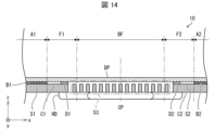
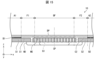
- FIG. 1 is a cross-sectional view showing an example of the configuration of a display device according to an embodiment of the present disclosure in an open state.
- FIG. 2 is a cross-sectional view showing an example of the configuration of a display device according to an embodiment of the present disclosure in a closed state.
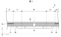
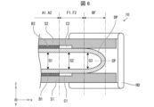
- a display device 10 according to an embodiment of the present disclosure is a foldable display device that includes a first support substrate S1, a second support substrate S2, and a flexible display panel DP and can be in an open state and a closed state.
- the display panel DP has a bending region BF, a first fixing region A1 fixed to the first support substrate S1, a second fixing region A2 fixed to the second support substrate S2, a first free region F1 located between the bending region BF and the first fixing region A1 and not fixed to the first support substrate S1, and a second free region F2 located between the bending region BF and the second fixing region A2 and not fixed to the second support substrate S2.
- the direction in which the display panel DP is located relative to the first support substrate S1 is defined as the z direction
- the direction in which the second support substrate S2 is located relative to the first support substrate S1 in the open state is defined as the x direction
- the direction perpendicular to the x direction and z direction is defined as the y direction.
- FIG. 3 is a diagram showing external forces and internal stresses in the bonding direction according to the present disclosure.
- a tensile force when a tensile force is applied to the display panel, a tensile stress acts to peel objects 1 and 2 from the bonding surface.
- a compressive force when a compressive force is applied to the display panel, a compressive stress acts to press objects 1 and 2 against the bonding surface.
- the tensile force and tensile stress shown on the left side of FIG. 3 are in the positive direction, and the compressive force and compressive stress shown on the right side of FIG. 3 are in the negative direction.
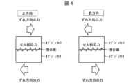
- FIG. 4 is a diagram showing external forces and internal stresses in the shear direction according to the present disclosure.
- a shear stress acts that tends to displace object 1 and object 2 from the joint surface.
- the force in the shear direction and the shear stress shown on the left side of FIG. 4 are positive directions, and the force in the shear direction and the shear stress shown on the right side of FIG. 4 are negative directions.
- peeling stress when the tensile stress and shear stress acting on the bonding surface exceed the bonding strength, object 1 and object 2 peel off from the bonding surface.
- peeling stress the tensile stress and shear stress that can cause peeling are collectively referred to as "peeling stress.” Note that the simulations described below (see Figures 18 to 23) are not actual experiments but numerical experiments on a computer. For simplification, in the stress simulations (see Figures 18 to 22), a model in which peeling does not occur was used, i.e., a model in which the bonding strength of the bonding surface is infinite.
- the configuration according to the present disclosure can reduce the occurrence of peeling inside the display device 10 compared to a configuration in which there is no free region between the fixed region and the bent region.
- the widths of the first free region F1 and the second free region F2 may each be 1 to 20 mm.
- “width” refers to the size in the x direction in the open state unless otherwise specified.
- the bending region BF is located between the first free region F1 and the second free region F2, and is continuously connected to the first free region F1 and the second free region F2.
- the first free region F1 is continuously connected to the first fixed region A1
- the second free region F2 is continuously connected to the second fixed region A2.
- the first fixed region A1 and the first free region F1 are located on the same plane as each other, and the second free region F2 and the second fixed region A2 are located on the same plane as each other.
- the display panel DP includes a cushion material BA as a layer closest to the first support substrate S1 and the second support substrate S2.
- the display panel DP includes a cushion material BA bonded to the flexible substrate 1 via an adhesive layer M1, and the cushion material BA is fixed to the first support substrate S1 and the second support substrate S2 via a first fixing material B1 and a second fixing material B2.
- the first support substrate S1 and the second support substrate S2 are each a metal plate, a resin plate, or a fiber-reinforced resin plate.
- the fiber-reinforced resin plate includes a carbon plate containing carbon fiber.
- the first support substrate S1 and the second support substrate S2 may be mechanically connected to each other in a movable manner by a hinge device HD.
- a first end of the hinge device HD may be directly or indirectly fixed to the first support substrate S1, and a second end of the hinge device HD may be directly or indirectly fixed to the second support substrate S2.
- the display panel DP can have a light-emitting element ED including an organic light-emitting layer or a quantum dot light-emitting layer as an emission layer EM.
- the display panel DP includes a flexible substrate 1, a transistor layer 2 including circuit elements such as transistors Tr and wiring, a display layer 3 including the light-emitting element ED, and a sealing layer 4 for preventing oxygen and moisture from entering the light-emitting element ED.
- the light-emitting element ED may have an anode E1 and a cathode E2, and an emission layer EM located between the anode E1 and the cathode E2.
- the light-emitting element ED may further have an electron injection layer EIL and an electron transport layer ETL for facilitating the injection of electrons into the emission layer EM, and a hole injection layer HIL and a hole transport layer HTL for facilitating the injection of holes into the emission layer EM.
- the display panel DP may include, above the sealing layer 4, an adhesive layer M2, a touch panel layer 5, an adhesive layer M3, a polarizing film 6, an adhesive layer M4, and a flexible cover 7, in this order.
- the quantum dots are semiconductor particles having a particle size of, for example, 100 nm or less, and may have II-VI group semiconductor compounds such as MgS, MgSe, MgTe, CaS, CaSe, CaTe, SrS, SrSe, SrTe, BaS, BaSe, BaTe, ZnS, ZnSe, ZnTe, CdS, CdSe, CdTe, HgS, HgSe, HgTe, and/or crystals of III-V group semiconductor compounds such as GaAs, GaP, InN, InAs, InP, InSb, and/or crystals of IV group semiconductor compounds such as Si and Ge.
- II-VI group semiconductor compounds such as MgS, MgSe, MgTe, CaS, CaSe, CaTe, SrS, SrSe, SrTe, BaS, BaSe, BaTe, ZnS, ZnSe, ZnTe, CdS
- the cushioning material BA may include multiple layers and may include an adhesive layer.
- Materials included in the cushioning material BA include polyethylene terephthalate (PET) resins, acrylic resins, urethane resins, polyester resins, stainless steel, aluminum, titanium, copper, etc.
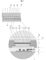
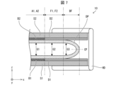
- FIG. 7 is a cross-sectional view showing an example of the configuration of a display device according to an embodiment of the present disclosure in a closed state.
- the display device 10 may have a first step adjustment material D1 adjacent to the first fixing material B1 and located between the first support substrate S1 and the first free area F1 of the display panel DP, and a second step adjustment material D2 adjacent to the second fixing material B2 and located between the second support substrate S2 and the second free area F2 of the display panel DP.
- the first fixing material B1 and the first step adjustment material D1 may be in contact with each other, and the second fixing material B2 and the second step adjustment material D2 may be in contact with each other.
- Fig. 9 is a cross-sectional view showing an example of the configuration of a display device according to an embodiment of the present disclosure in an open state.
- Fig. 10 is a cross-sectional view showing an example of the configuration of a display device according to an embodiment of the present disclosure in a closed state.
- the display device 10 may include a flexible substrate S3 that is continuously connected to the first support substrate S1 and the second support substrate S2 and is integrated with the first support substrate S1 and the second support substrate S2.
- FIG. 11 is a plan view showing an example of the configuration of the flexible substrate shown in FIGS. 9 and 10.
- the flexible substrate S3 may be a portion that has been shaped to reduce the second moment of area of the rigid substrate S4, and each of the first support substrate S1 and the second support substrate S2 may be a portion that has not been shaped to reduce the second moment of area of the rigid substrate S4.
- the shaping process that reduces the second moment of area of the portion of the rigid substrate S4 includes processing to form an opening K in that portion. Therefore, the flexible substrate S3 may include one or more openings K.
- the openings K may or may not penetrate all the way through.
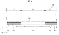
- FIG. 16 is a cross-sectional view showing the configuration of the display device according to Comparative Example 1 in an open state.
- the display device 100 according to Comparative Example 1 was a foldable display device that had a first support substrate 101, a second support substrate 102, and a flexible display panel 103, and could be in an open state or a closed state.
- the display panel 103 had a bending region 110, a first fixing region 111 fixed to the first support substrate 101 by a first fixing member 104, and a second fixing region 112 fixed to the second support substrate 102 by a second fixing member 105.
- the bending region 110 was directly connected to the first fixing region 111 and the second fixing region 112.
- the width of the bending region 110 according to Comparative Example 1 was approximately the same as the width of the bending region BF according to Example 1 of the present disclosure.
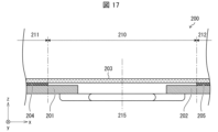
- FIG. 17 is a cross-sectional view showing the configuration of a display device according to Comparative Example 2 in an open state.
- the display device 200 according to Comparative Example 1 was a folding display device that had a first support substrate 201, a second support substrate 202, and a flexible display panel 203, and could be in an open state or a closed state.
- the display panel 203 had a bending region 210, a first fixing region 211 fixed to the first support substrate 201 by a first fixing member 204, and a second fixing region 212 fixed to the second support substrate 202 by a second fixing member 205.
- the bending region 210 was continuously connected to the first fixing region 211 and the second fixing region 212.
- the width of the bending region 210 according to Comparative Example 2 was the same as the total width of the first free region F1, the bending region BF, and the second free region F2 according to Example 1 of the present disclosure.
- Example 1 Comparative Example 1, and Comparative Example 2, the display panel DP, 103, 203 was flat in the open state, and the distance of the gap G1 between the first fixing area A1, 111, 211 and the second fixing area A2, 112, 212 in the closed state was 3.0 mm.
- FIG. 18 is a graph showing the results of a simulation of compressive stress and tensile stress occurring in the display panel in the closed state. On the vertical axis, positive indicates compressive stress and negative indicates tensile stress. As shown in FIG. 18, the graphs of Comparative Example 1 and Example 1 almost overlap, and the peak value of the tensile stress in Comparative Example 1 is 0.43 times that of Comparative Example 2, and in Example 1 it is 0.42 times that of Comparative Example 2. Peeling usually occurs between layers with the weakest adhesive strength. Typically, the adhesive strength between the display panel DP and the first and second support substrates S1, S2 is stronger than the adhesive strength inside the display panel DP, and peeling tends to occur inside the display panel DP. Therefore, compared to the display panel 203 of Comparative Example 2, peeling is less likely to occur inside the display panel DP in Example 1.
- the distance from the bending center CP in Example 1 to the boundary between the bending region BF and the first free region F1 was 2.4 mm to 3.2 mm.
- the distance from the bending center 115 in Comparative Example 1 to the boundary between the bending region 110 and the first fixed region 111 in Comparative Example 1 was 2.4 mm to 3.2 mm.
- the distance from the bending center 215 in Comparative Example 2 to the boundary between the bending region 210 and the first fixed region 211 was 4.8 mm to 6.2 mm.
- the peak positions of the tensile stress were in the first and second fixed regions 111, 112, 211, 212 in Comparative Examples 1 and 2, and in Example 1, they were in the first and second free regions F1, F2. Therefore, in the actual experiment, it is expected that the display panel DP will be less likely to peel off from the first and second support substrates S1, S2 in Example 1 compared to Comparative Examples 1 and 2.
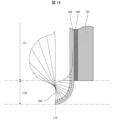
- FIG. 19 is a diagram showing the results of a simulation of compressive stress and tensile stress occurring in the display panel of Comparative Example 1 in the closed state superimposed on a cross-sectional view.
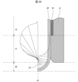
- FIG. 20 is a diagram showing the results of a simulation of compressive stress and tensile stress occurring in the display panel of Example 1 in the closed state superimposed on a cross-sectional view.
- the length of a line segment extending from the central surface of display panel 103, DP indicates the magnitude of tensile stress or compressive stress.
- the support substrate side relative to the central surface of display panel 103, DP indicates tensile stress, and the side opposite the support substrate indicates compressive stress.
- FIG. 21 is a diagram showing the results of a simulation of the shear stress generated in the display panel of Comparative Example 1 in the closed state superimposed on a cross-sectional view.
- FIG. 22 is a diagram showing the results of a simulation of the shear stress generated in the display panel of Example 1 in the closed state superimposed on a cross-sectional view.
- the length of the line extending from the central surface of the display panel 103, DP indicates the magnitude of the shear stress.
- the support substrate side of the central surface of the display panel 103, DP indicates negative shear stress, and the side opposite the support substrate indicates positive shear stress. Note that in this simulation, the direction from the center of bending toward the edge of the display panel was considered positive, and the opposite direction was considered negative.
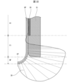
- FIG. 23 is a cross-sectional view showing the results of a simulation of the deformation and movement of the display panel in Example 1 in the closed state.
- Example 1 the display panel DP floated up from the first support substrate S1 in range R. Note that the distance of the float was very small.
Landscapes
- Physics & Mathematics (AREA)
- Optics & Photonics (AREA)
- Engineering & Computer Science (AREA)
- Chemical & Material Sciences (AREA)
- Crystallography & Structural Chemistry (AREA)
- Inorganic Chemistry (AREA)
- Nanotechnology (AREA)
- General Physics & Mathematics (AREA)
- Theoretical Computer Science (AREA)
- Electroluminescent Light Sources (AREA)
- Devices For Indicating Variable Information By Combining Individual Elements (AREA)
Abstract
Description
本開示は、表示装置に関する。 This disclosure relates to a display device.
特許文献1は、折り曲げが可能な電子デバイスの構成を開示している。
特許文献1に開示の構成では、フレキシブルディスプレイパネルがプレートに対して、屈曲領域の際まで接着固定されている。このため、剥離応力がディスプレイパネルに作用しやすく、フレキシブルディスプレイパネル内部の剥離が発生しやすい。剥離は、接合が最も弱い層間で進展しやすい。
In the configuration disclosed in
本開示の一態様に係る表示装置は、第1支持基板、第2支持基板、および可撓性の表示パネルを備え、開状態および閉状態を取り得る折り畳み型の表示装置であって、前記表示パネルは、屈曲領域と、前記第1支持基板に固定される第1固定領域と、前記第2支持基板に固定される第2固定領域と、前記屈曲領域および第1固定領域の間に位置し、前記第1支持基板に固定されない第1フリー領域と、前記屈曲領域および第2固定領域の間に位置し、前記第2支持基板に固定されない第2フリー領域とを有する、構成である。 A display device according to one embodiment of the present disclosure is a foldable display device that includes a first support substrate, a second support substrate, and a flexible display panel and can be in an open state or a closed state, and the display panel has a bending region, a first fixing region fixed to the first support substrate, a second fixing region fixed to the second support substrate, a first free region located between the bending region and the first fixing region and not fixed to the first support substrate, and a second free region located between the bending region and the second fixing region and not fixed to the second support substrate.
本開示に係る構成によれば、表示装置内部における剥離発生を低減することができる。 The configuration disclosed herein can reduce the occurrence of peeling inside the display device.
〔実施形態1〕
図1は、本開示の一実施形態に係る表示装置の構成の一例を、開状態で示す断面図である。図2は、本開示の一実施形態に係る表示装置の構成の一例を、閉状態で示す断面図である。図1および図2に示すように、本開示の実施形態1に係る表示装置10は、第1支持基板S1、第2支持基板S2、および可撓性の表示パネルDPを備え、開状態および閉状態を取り得る折り畳み型の表示装置である。表示パネルDPは、屈曲領域BFと、第1支持基板S1に固定される第1固定領域A1と、第2支持基板S2に固定される第2固定領域A2と、屈曲領域BFおよび第1固定領域A1の間に位置し、第1支持基板S1に固定されない第1フリー領域F1と、屈曲領域BFおよび第2固定領域A2の間に位置し、第2支持基板S2に固定されない第2フリー領域F2とを有する。
[Embodiment 1]
FIG. 1 is a cross-sectional view showing an example of the configuration of a display device according to an embodiment of the present disclosure in an open state. FIG. 2 is a cross-sectional view showing an example of the configuration of a display device according to an embodiment of the present disclosure in a closed state. As shown in FIGS. 1 and 2, a
本開示において、第1支持基板S1に対して表示パネルDPが在る方向をz方向とし、開状態で第1支持基板S1に対して第2支持基板S2が在る方向をx方向とし、x方向およびz方向と直交する方向をy方向とする。 In this disclosure, the direction in which the display panel DP is located relative to the first support substrate S1 is defined as the z direction, the direction in which the second support substrate S2 is located relative to the first support substrate S1 in the open state is defined as the x direction, and the direction perpendicular to the x direction and z direction is defined as the y direction.
図3は、本開示に係る接合方向の外力と内部応力とを示す図である。図3に示すように、表示パネルに引張力が加えられたとき、接合面からオブジェクト1およびオブジェクト2を引き剥がそうとする引張応力が作用する。また、表示パネルに圧縮力が加えられとき、接合面にオブジェクト1およびオブジェクト2を押し付けようとする圧縮応力が作用する。図3の左側に示す引張力および引張応力を正方向とし、図3の右側に示す圧縮力および圧縮応力を負方向とする。
FIG. 3 is a diagram showing external forces and internal stresses in the bonding direction according to the present disclosure. As shown in FIG. 3, when a tensile force is applied to the display panel, a tensile stress acts to
図4は、本開示に係るずれ方向の外力と内部応力とを示す図である。図4に示すように、接合体にずれ方向の力が加えられたとき、接合面からオブジェクト1およびオブジェクト2をずらそうとする剪断応力が作用する。図4の左側に示すずれ方向の力および剪断応力を正方向とし、図4の右側に示すずれ方向の力および剪断応力を負方向とする。
FIG. 4 is a diagram showing external forces and internal stresses in the shear direction according to the present disclosure. As shown in FIG. 4, when a force in the shear direction is applied to the joint, a shear stress acts that tends to displace
実物実験においては、接合面に作用する引張応力および剪断応力が接合強度を上回ったとき、オブジェクト1およびオブジェクト2が接合面から剥離する。本開示においては、剥離を招きうる引張応力および剪断応力を「剥離応力」と総称する。なお後述のシミュレーション(図18~図23参照)は、実物実験で無くコンピュータ上での数値実験である。応力のシミュレーション(図18~図22参照)では、簡単化のために、剥離が発生しないモデル、すなわち、接合面の接合強度が無限大であるモデルを採用した。
In actual experiments, when the tensile stress and shear stress acting on the bonding surface exceed the bonding strength,
図1および図2を参照して、本開示に係る構成によれば、表示パネルDPは、屈曲領域BFと、第1支持基板S1に固定される第1固定領域A1と、第2支持基板S2に固定される第2固定領域A2と、屈曲領域BFおよび第1固定領域A1の間に位置し、第1支持基板S1に固定されない第1フリー領域F1と、屈曲領域BFおよび第2固定領域A2の間に位置し、第2支持基板S2に固定されない第2フリー領域F2とを有する。このため、表示装置10の開閉によって第1フリー領域F1に外力が加わっても、第1フリー領域F1と第1支持基板S1との間または第1フリー領域F1内部の接合面に剥離応力が作用し難い。第2フリー領域F2に外力が加わっても、第2フリー領域F2と第2支持基板S2との間または第2フリー領域F2内部の接合面に剥離応力が作用し難い。
1 and 2, according to the configuration of the present disclosure, the display panel DP has a bending region BF, a first fixing region A1 fixed to the first support substrate S1, a second fixing region A2 fixed to the second support substrate S2, a first free region F1 located between the bending region BF and the first fixing region A1 and not fixed to the first support substrate S1, and a second free region F2 located between the bending region BF and the second fixing region A2 and not fixed to the second support substrate S2. Therefore, even if an external force is applied to the first free region F1 by opening and closing the
したがって、本開示に係る構成によれば、固定領域と屈曲領域との間にフリー領域が無い構成と比較して、表示装置10内部における剥離発生を低減することができる。本開示に係る構成において、表示装置10の開閉が第1固定領域A1および第2固定領域A2に影響しないように、第1フリー領域F1および第2フリー領域F2の幅はそれぞれ十分に大きいことが有益である。例えば、閉状態における第1固定領域F1と第2固定領域F2の間のギャップG1の距離が3〔mm〕である場合、第1フリー領域F1および第2フリー領域F2の幅はそれぞれ1~20〔mm〕であってよい。本開示において「幅」は、そうではないと断らない限り、開状態におけるx方向のサイズである。
Accordingly, the configuration according to the present disclosure can reduce the occurrence of peeling inside the
屈曲領域BFは、第1フリー領域F1および第2フリー領域F2の間の位置し、第1フリー領域F1および第2フリー領域F2と連続的に繋がる。第1フリー領域F1は第1固定領域A1に連続的に繋がり、第2フリー領域F2は第2固定領域A2に連続的に繋がる。第1固定領域A1および第1フリー領域F1は、互いと同一面上に位置し、第2フリー領域F2および第2固定領域A2は、互いと同一面上に位置する。 The bending region BF is located between the first free region F1 and the second free region F2, and is continuously connected to the first free region F1 and the second free region F2. The first free region F1 is continuously connected to the first fixed region A1, and the second free region F2 is continuously connected to the second fixed region A2. The first fixed region A1 and the first free region F1 are located on the same plane as each other, and the second free region F2 and the second fixed region A2 are located on the same plane as each other.
閉状態において、第1支持基板S1および第1フリー領域F1が互いと接触し、第2支持基板S2および第2フリー領域F2が互いと接触してよい。第1フリー領域F1は、開状態においても第1支持基板S1と接触してよく、第2フリー領域F2は、開状態においても第2支持基板S2と接触してよい。一方、閉状態において、屈曲領域BFは、第1支持基板S1および第2支持基板S2の何れとも接触しなくてよい。閉状態において、屈曲領域BFは断面視で、第1支持基板S1および第2支持基板S2の間に位置してよい。 In the closed state, the first support substrate S1 and the first free region F1 may be in contact with each other, and the second support substrate S2 and the second free region F2 may be in contact with each other. The first free region F1 may be in contact with the first support substrate S1 even in the open state, and the second free region F2 may be in contact with the second support substrate S2 even in the open state. On the other hand, in the closed state, the bending region BF may not be in contact with either the first support substrate S1 or the second support substrate S2. In the closed state, the bending region BF may be located between the first support substrate S1 and the second support substrate S2 in a cross-sectional view.
第1固定領域A1は、第1固定材B1を介して第1支持基板S1に固定され、第2固定領域A2は、第2固定材B2を介して第2支持基板S2に固定される。第1支持基板S1は、第1フリー領域F1と重なる部分の厚さが、第1固定材B1と重なる部分の厚さよりも大きくてよく、第2支持基板S2は、第2フリー領域F2と重なる部分の厚さが、第2固定材B2と重なる部分の厚さよりも大きくてよい。第1フリー領域F1と重なる部分と第1固定材B1と重なる部分との厚さの差は、第1固定材B1の厚さと同等であってよく、第2フリー領域F2と重なる部分と第2固定材B2と重なる部分との厚さの差は、第2固定材B2の厚さと同等であってよい。「厚さ」は、開状態におけるz方向のサイズである。 The first fixing region A1 is fixed to the first support substrate S1 via the first fixing material B1, and the second fixing region A2 is fixed to the second support substrate S2 via the second fixing material B2. The first support substrate S1 may have a thickness greater than the thickness of the portion overlapping with the first free region F1, and the second support substrate S2 may have a thickness greater than the thickness of the portion overlapping with the second free region F2. The difference in thickness between the portion overlapping with the first free region F1 and the portion overlapping with the first fixing material B1 may be equal to the thickness of the first fixing material B1, and the difference in thickness between the portion overlapping with the second free region F2 and the portion overlapping with the second fixing material B2 may be equal to the thickness of the second fixing material B2. "Thickness" refers to the size in the z direction in the open state.
本開示において、第1サイズと第2サイズとの差が、第1サイズの10%以下、または10〔μm〕以下であるとき、第1サイズは第2サイズと同等であると表現する。 In this disclosure, when the difference between the first size and the second size is 10% or less of the first size, or 10 μm or less, the first size is said to be equal to the second size.
閉状態において、第1固定領域A1および第2固定領域A2の間のギャップG1の距離と、第1フリー領域F1および第2フリー領域F2の間のギャップG2の距離が等しくてよい。閉状態において、屈曲領域BFは、屈曲領域BF同士の間のギャップG3の距離が第1フリー領域F1および第2フリー領域F2の間のギャップG2の距離より小さくなるように屈曲してよく、例えば、U字形状となってよい(図2参照)。 In the closed state, the distance of the gap G1 between the first fixed region A1 and the second fixed region A2 may be equal to the distance of the gap G2 between the first free region F1 and the second free region F2. In the closed state, the bent region BF may be bent such that the distance of the gap G3 between the bent regions BF is smaller than the distance of the gap G2 between the first free region F1 and the second free region F2, and may be, for example, U-shaped (see FIG. 2).
図1を参照して、表示パネルDPは、最も第1支持基板S1および第2支持基板S2に近い層として、クッション材BAを備える。例えば、表示パネルDPは、フレキシブル基板1に粘着層M1を介して接着されたクッション材BAを備え、クッション材BAが第1固定材B1および第2固定材B2を介して第1支持基板S1および第2支持基板S2に固定される。第1支持基板S1および第2支持基板S2はそれぞれ、金属板、樹脂板、および繊維強化樹脂板の何れかである。繊維強化樹脂板は、炭素繊維を含むカーボン板を含む。第1支持基板S1および第2支持基板S2は、ヒンジ装置HDによって、運動可能に機械的に接続されてよい。ヒンジ装置HDの第1端は、第1支持基板S1に直接的または間接的に固定されてよく、ヒンジ装置HDの第2端は、第2支持基板S2に直接的または間接的に固定されてよい。
Referring to FIG. 1, the display panel DP includes a cushion material BA as a layer closest to the first support substrate S1 and the second support substrate S2. For example, the display panel DP includes a cushion material BA bonded to the
図5は、本開示の一実施形態に係る表示パネルの構成の一例を示す断面図である。図5に示すように、表示パネルDPは、発光層EMとして有機発光層または量子ドット発光層を含む発光素子EDを有することができる。例えば表示パネルDPは、フレキシブル基板1、トランジスタTrなどの回路素子および配線を含むトランジスタ層2、発光素子EDを含む表示層3、発光素子EDに酸素および水分が侵入するのを防止するための封止層4を含む。発光素子EDは、アノードE1およびカソードE2と、アノードE1およびカソードE2の間に位置する発光層EMとを有してよい。例えば発光素子EDはさらに、発光層EMに電子を注入し易くするための電子注入層EILおよび電子輸送層ETLと、発光層EMに正孔を注入し易くするための正孔注入層HILおよび正孔輸送層HTLと、を有してよい。例えば、表示パネルDPは、封止層4より上層に、粘着層M2、タッチパネル層5、粘着層M3、偏光フィルム6、粘着層M4および可撓性カバー7をこの順に備えてよい。
5 is a cross-sectional view showing an example of the configuration of a display panel according to an embodiment of the present disclosure. As shown in FIG. 5, the display panel DP can have a light-emitting element ED including an organic light-emitting layer or a quantum dot light-emitting layer as an emission layer EM. For example, the display panel DP includes a
量子ドットは、最大幅が100nm以下のドットを意味する。量子ドットの形状は、上記最大幅を満たす範囲であればよく、特に制約されず、球状の立体形状(円状の断面形状)に限定されるものではない。例えば、多角形状の断面形状、棒状の立体形状、枝状の立体形状、表面に凹凸を有す立体形状でもよく、または、それらの組合せでもよい。本実施例においては、量子ドットは、例えば、100nm以下の粒子サイズを有する半導体微粒子であり、MgS、MgSe、MgTe、CaS、CaSe、CaTe、SrS、SrSe、SrTe、BaS、BaSe、BaTe、ZnS、ZnSe、ZnTe、CdS、CdSe、CdTe、HgS、HgSe、HgTe等のII-VI族半導体化合物、及び/又は、GaAs、GaP、InN、InAs、InP、InSb等のIII-V族半導体化合物の結晶、及び/又は、Si、Ge等のIV族半導体化合物の結晶を有することができる。また、量子ドットは、例えば、上記の半導体結晶をコアとして、当該コアをバンドギャップの大きいシェル材料でオーバーコートしたコア/シェル構造を有していてもよい。なお、シェルは必ずしもコアを完全に覆う必要はなく、コア上の一部にでも形成されていればよい。 Quantum dots refer to dots with a maximum width of 100 nm or less. The shape of the quantum dots is not particularly restricted as long as it satisfies the above maximum width, and is not limited to a spherical three-dimensional shape (circular cross-sectional shape). For example, they may have a polygonal cross-sectional shape, a rod-shaped three-dimensional shape, a branch-shaped three-dimensional shape, a three-dimensional shape with unevenness on the surface, or a combination of these. In this embodiment, the quantum dots are semiconductor particles having a particle size of, for example, 100 nm or less, and may have II-VI group semiconductor compounds such as MgS, MgSe, MgTe, CaS, CaSe, CaTe, SrS, SrSe, SrTe, BaS, BaSe, BaTe, ZnS, ZnSe, ZnTe, CdS, CdSe, CdTe, HgS, HgSe, HgTe, and/or crystals of III-V group semiconductor compounds such as GaAs, GaP, InN, InAs, InP, InSb, and/or crystals of IV group semiconductor compounds such as Si and Ge. In addition, the quantum dots may have a core/shell structure in which the above-mentioned semiconductor crystal is used as a core and the core is overcoated with a shell material having a large band gap. Note that the shell does not necessarily have to completely cover the core, and may be formed on at least a part of the core.
クッション材BAは、複数の層を含んでよく、粘着層を含んでよい。クッション材BAに含まれる材料として、ポリエチレンテレフタラート(PET)系樹脂、アクリル系樹脂、ウレタン系樹脂、ポリエステル系樹脂、ステンレス、アルミニウム、チタン、銅などが挙げられる。 The cushioning material BA may include multiple layers and may include an adhesive layer. Materials included in the cushioning material BA include polyethylene terephthalate (PET) resins, acrylic resins, urethane resins, polyester resins, stainless steel, aluminum, titanium, copper, etc.
〔実施形態2〕
本開示の他の実施形態について、以下に説明する。なお、説明の便宜上、上記実施形態にて説明した部材と同じ機能を有する部材については、同じ符号を付記し、その説明を繰り返さない。
[Embodiment 2]
Other embodiments of the present disclosure will be described below. For ease of explanation, the same reference numerals will be used to designate components having the same functions as those described in the above embodiment, and the description thereof will not be repeated.
図6は、本開示の一実施形態に係る表示装置の構成の一例を、閉状態で示す断面図である。図6に示すように、表示装置10は、第1固定材B1に隣接し、第1支持基板S1および表示パネルDPの第1フリー領域F1の間に位置する第1空隙C1と、第2固定材B2に隣接し、第2支持基板S2および表示パネルDPの第2フリー領域F2の間に位置する第2空隙C2と、を有することがある。第1空隙C1の幅は、第1固定材B1の幅よりも小さくてよく、第2空隙C2の幅は、第2固定材B2の幅よりも小さくてよい。
FIG. 6 is a cross-sectional view showing an example of the configuration of a display device according to an embodiment of the present disclosure in a closed state. As shown in FIG. 6, the
本開示において「ある部材が別の部材に隣接する」とは、ある部材と別の部材との間に空隙があり、ある部材が空隙を介して別の部材と隣り合っている場合と、ある部材が別の部材と接触して、隙間なく隣り合っている場合と、を包含する。本開示において、「空隙がある部材に隣接する」とは、空隙とある部材との間に別の部材が無く、空隙がある部材と接触して隣り合っている場合を意味する。 In this disclosure, "a member adjacent to another member" includes cases where there is a gap between the two members and the member is adjacent to the other member through the gap, and cases where the member is in contact with the other member and adjacent to it with no gap. In this disclosure, "adjacent to a member with a gap" means that there is no other member between the gap and the member and the member is in contact with the member with the gap and adjacent to it.
〔実施形態3〕
図7は、本開示の一実施形態に係る表示装置の構成の一例を、閉状態で示す断面図である。図7に示すように、表示装置10は、第1固定材B1に隣接し、第1支持基板S1および表示パネルDPの第1フリー領域F1の間に位置する第1段差調整材D1と、第2固定材B2に隣接し、第2支持基板S2および表示パネルDPの第2フリー領域F2の間に位置する第2段差調整材D2と、を有することがある。第1固定材B1および第1段差調整材D1が互いと接触してよく、第2固定材B2および第2段差調整材D2が互いと接触してよい。
[Embodiment 3]
7 is a cross-sectional view showing an example of the configuration of a display device according to an embodiment of the present disclosure in a closed state. As shown in FIG. 7, the
第1支持基板S1は、第1フリー領域F1と重なる部分の厚さが、第1固定材B1と重なる部分の厚さと同等であってよく、第2支持基板S2は、第2フリー領域F2と重なる部分の厚さが、第2固定材B2と重なる部分の厚さと同等であってよい。第1段差調整材D1の厚さは、第1固定材B1の厚さと同等であってよく、第2段差調整材D2の厚さは、第2固定材B2の厚さと同等であってよい。 The thickness of the portion of the first support substrate S1 that overlaps with the first free region F1 may be equal to the thickness of the portion that overlaps with the first fixing material B1, and the thickness of the portion of the second support substrate S2 that overlaps with the second free region F2 may be equal to the thickness of the portion that overlaps with the second fixing material B2. The thickness of the first step adjustment material D1 may be equal to the thickness of the first fixing material B1, and the thickness of the second step adjustment material D2 may be equal to the thickness of the second fixing material B2.
閉状態において、第1段差調整材D1および表示パネルDPの第1フリー領域F1が互いと接触してよく、第2段差調整材D2および表示パネルDPの第2フリー領域F2が互いと接触してよい。 In the closed state, the first step adjustment material D1 and the first free area F1 of the display panel DP may be in contact with each other, and the second step adjustment material D2 and the second free area F2 of the display panel DP may be in contact with each other.
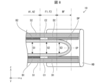
〔実施形態4〕
図8は、本開示の一実施形態に係る表示装置の構成の一例を、閉状態で示す断面図である。図8に示すように、表示装置10は、第1段差調整材D1および第2段差調整材D2を有し、さらに、第1固定材B1および第1段差調整材D1の間に位置する第1空隙C1と、第2固定材B2および第2段差調整材D2の間に位置する第2空隙C2と、を有することがある。
[Embodiment 4]
8 is a cross-sectional view showing an example of the configuration of a display device according to an embodiment of the present disclosure in a closed state. As shown in FIG. 8, the
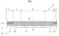
〔実施形態5〕
図9は、本開示の一実施形態に係る表示装置の構成の一例を、開状態で示す断面図である。図10は、本開示の一実施形態に係る表示装置の構成の一例を、閉状態で示す断面図である。図9および図10に示すように、表示装置10は、第1支持基板S1および第2支持基板S2に連続的に繋がり、第1支持基板S1および第2支持基板S2と一体である可撓性基板S3を含むことがある。
[Embodiment 5]
Fig. 9 is a cross-sectional view showing an example of the configuration of a display device according to an embodiment of the present disclosure in an open state. Fig. 10 is a cross-sectional view showing an example of the configuration of a display device according to an embodiment of the present disclosure in a closed state. As shown in Figs. 9 and 10, the
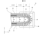
図11は、図9および図10に示した可撓性基板の構成の一例を示す平面図である。図11に示すように、可撓性基板S3は、剛性基板S4の断面二次モーメントを小さくするように形状加工された部分であってよく、第1支持基板S1および第2支持基板S2それぞれは当該剛性基板S4の断面二次モーメントを小さくするように形状加工されていない部分であってよい。剛性基板S4の部分の断面二次モーメントを小さくする形状加工は、当該部分に開口Kを形成する加工を含む。したがって、可撓性基板S3は、1個以降の開口Kを含んでよい。開口Kは、貫通してもしなくてもよい。 FIG. 11 is a plan view showing an example of the configuration of the flexible substrate shown in FIGS. 9 and 10. As shown in FIG. 11, the flexible substrate S3 may be a portion that has been shaped to reduce the second moment of area of the rigid substrate S4, and each of the first support substrate S1 and the second support substrate S2 may be a portion that has not been shaped to reduce the second moment of area of the rigid substrate S4. The shaping process that reduces the second moment of area of the portion of the rigid substrate S4 includes processing to form an opening K in that portion. Therefore, the flexible substrate S3 may include one or more openings K. The openings K may or may not penetrate all the way through.
図9および図10を参照して、表示パネルDPの屈曲領域BFは、可撓性基板S3と接触してよく、第1フリー領域F1および第2フリー領域F2が、可撓性基板S3と接触してよい。 Referring to Figures 9 and 10, the bent region BF of the display panel DP may be in contact with the flexible substrate S3, and the first free region F1 and the second free region F2 may be in contact with the flexible substrate S3.
図12~図14はそれぞれ、本開示の一実施形態に係る表示装置の構成の変形例を、開状態で示す断面図である。図12~図14に示すように、実施形態5に係る構成は、前述の実施形態2~4に係る構成と組み合わせ可能である。
FIGS. 12 to 14 are cross-sectional views showing modified configurations of a display device according to an embodiment of the present disclosure in an open state. As shown in FIG. 12 to FIG. 14, the configuration according to embodiment 5 can be combined with the configurations according to
〔実施形態6〕 [Embodiment 6]
図15は、本開示の一実施形態に係る表示装置の構成の一例を、開状態で示す断面図である。図15に示すように、表示パネルDPの屈曲領域BFは、粘着層M5を介して可撓性基板S3に接着されていてよい。表示装置10は、第1固定材B1および粘着層M5の間に位置する第1空隙C1と、第2固定材B2および粘着層M5の間に位置する第2空隙C2と、を有してもよい。
FIG. 15 is a cross-sectional view showing an example of the configuration of a display device according to an embodiment of the present disclosure in an open state. As shown in FIG. 15, the bending region BF of the display panel DP may be adhered to a flexible substrate S3 via an adhesive layer M5. The
本開示の一実施例について以下に説明する。本開示の実施例1として、図1および図2に示した構成の表示装置10を作成した。また、比較例1および比較例2に係る表示装置100、200も作成した。
An embodiment of the present disclosure will be described below. As
図16は、比較例1に係る表示装置の構成を、開状態で示す断面図である。図16に示すように、比較例1に係る表示装置100は、第1支持基板101、第2支持基板102、および可撓性の表示パネル103を備え、開状態および閉状態を取り得る折り畳み型の表示装置であった。表示パネル103は、屈曲領域110と、第1支持基板101に第1固定部材104で固定される第1固定領域111と、第2支持基板102に第2固定部材105で固定される第2固定領域112とを有した。屈曲領域110は、第1固定領域111および第2固定領域112に直接繋がっていた。比較例1に係る屈曲領域110の幅は、本開示の実施例1に係る屈曲領域BFの幅と略同一であった。
FIG. 16 is a cross-sectional view showing the configuration of the display device according to Comparative Example 1 in an open state. As shown in FIG. 16, the
図17は、比較例2に係る表示装置の構成を、開状態で示す断面図である。図17に示すように、比較例1に係る表示装置200は、第1支持基板201、第2支持基板202、および可撓性の表示パネル203を備え、開状態および閉状態を取り得る折り畳み型の表示装置であった。表示パネル203は、屈曲領域210と、第1支持基板201に第1固定部材204で固定される第1固定領域211と、第2支持基板202に第2固定部材205で固定される第2固定領域212とを有した。屈曲領域210は、第1固定領域211および第2固定領域212に連続的に繋がっていた。比較例2に係る屈曲領域210の幅は、本開示の実施例1に係る第1フリー領域F1と屈曲領域BFと第2フリー領域F2との合計の幅と同一であった。
FIG. 17 is a cross-sectional view showing the configuration of a display device according to Comparative Example 2 in an open state. As shown in FIG. 17, the
実施例1、比較例1および比較例2の何れについても、開状態で表示パネルDP、103、203が平坦であり、閉状態で第1固定領域A1、111、211と第2固定領域A2、112、212との間のギャップG1の距離が3.0〔mm〕であった。 In all of Example 1, Comparative Example 1, and Comparative Example 2, the display panel DP, 103, 203 was flat in the open state, and the distance of the gap G1 between the first fixing area A1, 111, 211 and the second fixing area A2, 112, 212 in the closed state was 3.0 mm.
図18は、閉状態で表示パネルに発生する圧縮応力および引張応力のシミュレーション結果のグラフを示す図である。縦軸は、正が圧縮応力を示し、負が引張応力を示す。図18に示すように、比較例1および実施例1のグラフがほぼ重なり、引張応力のピーク値は、比較例1が比較例2の0.43倍であり、実施例1が比較例2の0.42倍であった。剥離は通常、接着力が最も弱い層間で発生する。典型的には、表示パネルDPと第1および第2支持基板S1,S2との間の接着力は、表示パネルDP内部の接着力よりも強く、剥離は表示パネルDP内部で発生する傾向にある。したがって、比較例2の表示パネル203と比較して、実施例1では表示パネルDP内部での剥離が発生しにくい。
FIG. 18 is a graph showing the results of a simulation of compressive stress and tensile stress occurring in the display panel in the closed state. On the vertical axis, positive indicates compressive stress and negative indicates tensile stress. As shown in FIG. 18, the graphs of Comparative Example 1 and Example 1 almost overlap, and the peak value of the tensile stress in Comparative Example 1 is 0.43 times that of Comparative Example 2, and in Example 1 it is 0.42 times that of Comparative Example 2. Peeling usually occurs between layers with the weakest adhesive strength. Typically, the adhesive strength between the display panel DP and the first and second support substrates S1, S2 is stronger than the adhesive strength inside the display panel DP, and peeling tends to occur inside the display panel DP. Therefore, compared to the
実施例1の屈曲中心CPからの距離は、屈曲領域BFと第1フリー領域F1との境界までが2.4〔mm〕~3.2〔mm〕であった。比較例1の屈曲中心115からの距離は、比較例1の屈曲領域110と第1固定領域111との境界までが2.4〔mm〕~3.2〔mm〕であった。比較例2の屈曲中心215からの距離は、屈曲領域210と第1固定領域211との境界までが4.8〔mm〕~6.2〔mm〕であった。
The distance from the bending center CP in Example 1 to the boundary between the bending region BF and the first free region F1 was 2.4 mm to 3.2 mm. The distance from the
引張応力のピーク位置が、比較例1および比較例2では、第1および第2固定領域111、112、211、212にあり、実施例1では、第1および第2フリー領域F1、F2にあった。したがって、実物実験において、比較例1および比較例2と比較して、実施例1に係る第1および第2支持基板S1、S2から表示パネルDPが剥離し難いことが予想される。
The peak positions of the tensile stress were in the first and second
図19は、閉状態で比較例1に係る表示パネルに発生する圧縮応力および引張応力のシミュレーション結果を断面図に重ねて示す図である。図20は、閉状態で実施例1に係る表示パネルに発生する圧縮応力および引張応力のシミュレーション結果を断面図に重ねて示す図である。グラフ120,20は、表示パネル103,DPの中央面から伸びる線分の長さが、引張応力または圧縮応力の大きさを示す。表示パネル103,DPの中央面に対して支持基板側が引張応力を示し、支持基板と反対側が圧縮応力を示す。
FIG. 19 is a diagram showing the results of a simulation of compressive stress and tensile stress occurring in the display panel of Comparative Example 1 in the closed state superimposed on a cross-sectional view. FIG. 20 is a diagram showing the results of a simulation of compressive stress and tensile stress occurring in the display panel of Example 1 in the closed state superimposed on a cross-sectional view. In
図21は、閉状態で比較例1に係る表示パネルに発生する剪断応力のシミュレーション結果を断面図に重ねて示す図である。図22は、閉状態で実施例1に係る表示パネルに発生する剪断応力のシミュレーション結果を断面図に重ねて示す図である。グラフ130,30は、表示パネル103,DPの中央面から伸びる線分の長さが、剪断応力の大きさを示す。表示パネル103,DPの中央面に対して支持基板側が、負の剪断応力を示し、支持基板と反対側が、正の剪断応力を示す。なお、今回のシミュレーションでは、屈曲中心から表示パネルの端の方向に向かう方向を正、その逆方向を負とした。
FIG. 21 is a diagram showing the results of a simulation of the shear stress generated in the display panel of Comparative Example 1 in the closed state superimposed on a cross-sectional view. FIG. 22 is a diagram showing the results of a simulation of the shear stress generated in the display panel of Example 1 in the closed state superimposed on a cross-sectional view. In
図19および図21に示すように、比較例1では引張応力および正の剪断応力が生じる範囲が、第1固定領域111に含まれた。第1固定領域111で表示パネル103は第1支持基板101に固定されているため、実物実験において、引張応力および正の剪断応力によって表示パネル103が第1支持基板101から剥離し易いことが予想される。一方、図20および図22に示すように、実施例1では引張応力および正の剪断応力が生じる範囲が、第1フリー領域F1に含まれた。第1フリー領域F1で表示パネルDPは固定されていないため、実物実験において、表示パネルDPが変形および移動して、引張応力および正の剪断応力を緩和し、表示パネルDPが第1支持基板S1から剥離し難いことが予想される。
As shown in Figures 19 and 21, in Comparative Example 1, the range in which tensile stress and positive shear stress occur was included in the
図23は、閉状態での実施例1に係る表示パネルの変形および移動のシミュレーション結果を示す断面図である。図23に示すように、実施例1では、範囲Rで表示パネルDPが第1支持基板S1から浮き上がった。なお、浮き上がりの距離は微小であった。 FIG. 23 is a cross-sectional view showing the results of a simulation of the deformation and movement of the display panel in Example 1 in the closed state. As shown in FIG. 23, in Example 1, the display panel DP floated up from the first support substrate S1 in range R. Note that the distance of the float was very small.
本開示は上述した各実施形態に限定されるものではなく、請求項に示した範囲で種々の変更が可能であり、異なる実施形態にそれぞれ開示された技術的手段を適宜組み合わせて得られる実施形態についても本開示の技術的範囲に含まれる。さらに、各実施形態にそれぞれ開示された技術的手段を組み合わせることにより、新しい技術的特徴を形成することができる。 This disclosure is not limited to the above-described embodiments, and various modifications are possible within the scope of the claims. The technical scope of this disclosure also includes embodiments obtained by appropriately combining the technical means disclosed in different embodiments. Furthermore, new technical features can be formed by combining the technical means disclosed in each embodiment.
10 表示装置
A1 第1固定領域
A2 第2固定領域
B1 第1固定材
B2 第2固定材
BA クッション材
BF 屈曲領域
C1 第1空隙
C2 第2空隙
CP、115、215 屈曲中心
D1 第1段差調整材
D2 第2段差調整材
DP、103、203 表示パネル
ED 発光素子
F1 第1フリー領域
F2 第2フリー領域
G1、G2、G3 ギャップ
K 開口
M1、M2、M3、M4、M5 粘着層
S1 第1支持基板
S2 第2支持基板
S3 可撓性基板
S4 剛性基板
10 Display device A1 First fixing area A2 Second fixing area B1 First fixing material B2 Second fixing material BA Cushion material BF Bending area C1 First gap C2 Second gap CP, 115, 215 Bending center D1 First step adjustment material D2 Second step adjustment material DP, 103, 203 Display panel ED Light emitting element F1 First free area F2 Second free area G1, G2, G3 Gap K Opening M1, M2, M3, M4, M5 Adhesive layer S1 First support substrate S2 Second support substrate S3 Flexible substrate S4 Rigid substrate
Claims (25)
前記表示パネルは、屈曲領域と、前記第1支持基板に固定される第1固定領域と、前記第2支持基板に固定される第2固定領域と、前記屈曲領域および前記第1固定領域の間に位置し、前記第1支持基板に固定されない第1フリー領域と、前記屈曲領域および前記第2固定領域の間に位置し、前記第2支持基板に固定されない第2フリー領域とを有する、表示装置。 A foldable display device that includes a first support substrate, a second support substrate, and a flexible display panel and can be in an open state and a closed state,
A display device, wherein the display panel has a bending region, a first fixing region fixed to the first support substrate, a second fixing region fixed to the second support substrate, a first free region located between the bending region and the first fixing region and not fixed to the first support substrate, and a second free region located between the bending region and the second fixing region and not fixed to the second support substrate.
前記第2フリー領域は、前記開状態において前記第2支持基板に接触する、請求項4に記載の表示装置。 the first free region contacts the first support substrate in the open state;
The display device according to claim 4 , wherein the second free region is in contact with the second support substrate in the open state.
前記第2固定領域が第2固定材を介して前記第2支持基板に固定される、請求項1~7のいずれか1項に記載の表示装置。 the first fixing region is fixed to the first support substrate via a first fixing material;
The display device according to claim 1 , wherein the second fixing region is fixed to the second support substrate via a second fixing material.
前記第2支持基板は、前記第2フリー領域と重なる部分の厚さが、前記第2固定材と重なる部分の厚さよりも大きい、請求項8に記載の表示装置。 a thickness of a portion of the first support substrate overlapping the first free region is greater than a thickness of a portion of the first support substrate overlapping the first fixing material;
The display device according to claim 8 , wherein a thickness of the second support substrate at a portion overlapping the second free region is greater than a thickness of a portion overlapping the second fixing material.
前記第2固定材に隣接し、前記第2支持基板および前記第2フリー領域の間に位置する第2空隙とを有する、請求項9に記載の表示装置。 a first gap adjacent to the first fixing material and located between the first support substrate and the first free region;
The display device according to claim 9 , further comprising: a second gap adjacent to the second fixing material and located between the second supporting substrate and the second free region.
前記第2固定材に隣接し、前記第2支持基板および前記第2フリー領域の間に位置する第2段差調整材とを有する、請求項8に記載の表示装置。 a first step adjustment material adjacent to the first fixing material and located between the first support substrate and the first free region;
The display device according to claim 8 , further comprising: a second step adjustment material adjacent to the second fixing material and located between the second supporting substrate and the second free region.
Priority Applications (1)
| Application Number | Priority Date | Filing Date | Title |
|---|---|---|---|
| PCT/JP2023/030117 WO2025041255A1 (en) | 2023-08-22 | 2023-08-22 | Display device |
Applications Claiming Priority (1)
| Application Number | Priority Date | Filing Date | Title |
|---|---|---|---|
| PCT/JP2023/030117 WO2025041255A1 (en) | 2023-08-22 | 2023-08-22 | Display device |
Publications (1)
| Publication Number | Publication Date |
|---|---|
| WO2025041255A1 true WO2025041255A1 (en) | 2025-02-27 |
Family
ID=94731939
Family Applications (1)
| Application Number | Title | Priority Date | Filing Date |
|---|---|---|---|
| PCT/JP2023/030117 Pending WO2025041255A1 (en) | 2023-08-22 | 2023-08-22 | Display device |
Country Status (1)
| Country | Link |
|---|---|
| WO (1) | WO2025041255A1 (en) |
Citations (2)
| Publication number | Priority date | Publication date | Assignee | Title |
|---|---|---|---|---|
| US20200319672A1 (en) * | 2019-03-11 | 2020-10-08 | Samsung Electronics Co., Ltd. | Electronic device including foldable conductive plate |
| CN115311942A (en) * | 2022-07-22 | 2022-11-08 | 昆山国显光电有限公司 | Display module and display device |
-
2023
- 2023-08-22 WO PCT/JP2023/030117 patent/WO2025041255A1/en active Pending
Patent Citations (2)
| Publication number | Priority date | Publication date | Assignee | Title |
|---|---|---|---|---|
| US20200319672A1 (en) * | 2019-03-11 | 2020-10-08 | Samsung Electronics Co., Ltd. | Electronic device including foldable conductive plate |
| CN115311942A (en) * | 2022-07-22 | 2022-11-08 | 昆山国显光电有限公司 | Display module and display device |
Similar Documents
| Publication | Publication Date | Title |
|---|---|---|
| CN100380574C (en) | Peeling method and method for manufacturing semiconductor device | |
| CN108987434B (en) | Electroluminescence device, flexible display device and manufacturing method thereof | |
| CN111976249B (en) | Composite foam layer and display module | |
| US11175764B2 (en) | Touch display device | |
| US20230229196A1 (en) | Display module and display device | |
| US11462699B2 (en) | Display panel, method for manufacturing the same and display device | |
| JP7237005B2 (en) | Display substrate, display device, display substrate manufacturing method | |
| EP3498880A1 (en) | Mask plate and evaporation device | |
| CN113284423B (en) | Flexible display panel and display device | |
| JP2018170426A (en) | Light emitting device | |
| CN109728195B (en) | Display panel and display device | |
| US11793037B2 (en) | Display panel and display device | |
| CN111653205B (en) | Stretchable display panel and display device | |
| WO2025041255A1 (en) | Display device | |
| US20200119110A1 (en) | Flexible organic light emitting diode display device and method of fabricating same | |
| WO2023087335A1 (en) | Display panel and preparation method therefor | |
| US12057034B2 (en) | Display device | |
| US20250349230A1 (en) | Elastic member | |
| CN108550554A (en) | Display panel and display device | |
| CN111162203A (en) | Back film and preparation method thereof, flexible display device and preparation method thereof, knife die | |
| US7911138B2 (en) | Encapsulation cap and display device including the same | |
| US11744140B2 (en) | Flexible display panel and fabrication method thereof | |
| WO2026044916A1 (en) | Display module and display device | |
| DE102016125938A1 (en) | Flexible, optoelectronic component and method for producing the flexible, optoelectronic component | |
| TW202315495A (en) | Electronic device and manufacturing method comprising the same |
Legal Events
| Date | Code | Title | Description |
|---|---|---|---|
| 121 | Ep: the epo has been informed by wipo that ep was designated in this application |
Ref document number: 23949716 Country of ref document: EP Kind code of ref document: A1 |
|
| NENP | Non-entry into the national phase |
Ref country code: DE |