WO2025041234A1 - 波長変換装置および制御方法 - Google Patents
波長変換装置および制御方法 Download PDFInfo
- Publication number
- WO2025041234A1 WO2025041234A1 PCT/JP2023/030046 JP2023030046W WO2025041234A1 WO 2025041234 A1 WO2025041234 A1 WO 2025041234A1 JP 2023030046 W JP2023030046 W JP 2023030046W WO 2025041234 A1 WO2025041234 A1 WO 2025041234A1
- Authority
- WO
- WIPO (PCT)
- Prior art keywords
- light
- wavelength
- intensity
- optical
- signal
- Prior art date
- Legal status (The legal status is an assumption and is not a legal conclusion. Google has not performed a legal analysis and makes no representation as to the accuracy of the status listed.)
- Pending
Links
Images


Classifications
-
- G—PHYSICS
- G02—OPTICS
- G02F—OPTICAL DEVICES OR ARRANGEMENTS FOR THE CONTROL OF LIGHT BY MODIFICATION OF THE OPTICAL PROPERTIES OF THE MEDIA OF THE ELEMENTS INVOLVED THEREIN; NON-LINEAR OPTICS; FREQUENCY-CHANGING OF LIGHT; OPTICAL LOGIC ELEMENTS; OPTICAL ANALOGUE/DIGITAL CONVERTERS
- G02F1/00—Devices or arrangements for the control of the intensity, colour, phase, polarisation or direction of light arriving from an independent light source, e.g. switching, gating or modulating; Non-linear optics
- G02F1/35—Non-linear optics
- G02F1/37—Non-linear optics for second-harmonic generation
Definitions
- a wavelength conversion technology that uses difference frequency generation (DFG) by a nonlinear optical medium is known.
- Wavelength conversion technology that uses DFG can convert light in a wavelength band used in optical fiber communications, for example, into light in a different wavelength band all at once.
- wavelength conversion technology can be applied to optical routing technologies, such as optical routing in wavelength division multiplexing (WDM) systems, or wavelength collision avoidance in optical routing. Therefore, wavelength conversion technology is positioned as one of the key technologies for building large-capacity optical communication networks.
- WDM wavelength division multiplexing
- One non-limiting objective of this disclosure is to simplify the control required to stably operate a wavelength conversion device that uses a nonlinear optical medium.
- a wavelength conversion device includes a wavelength converter using a nonlinear optical medium, a wavelength separation filter that separates a portion of the output light generated in the wavelength converter by parametric fluorescence in response to the input of excitation light to the nonlinear optical medium, a detection circuit that detects the intensity of the light separated by the wavelength separation filter and the slope of the change in the intensity, and a control circuit that individually controls the intensity of the excitation light and the temperature of the wavelength converter based on the intensity and the slope.
- a control method includes separating, by a wavelength separation filter, a portion of output light generated in a wavelength converter by parametric fluorescence in response to input of excitation light to the wavelength converter using a nonlinear optical medium, detecting the intensity of the light separated by the wavelength separation filter and the slope of the change in the intensity by a detection circuit, and individually controlling the intensity of the excitation light and the temperature of the wavelength converter by a control circuit based on the detected intensity and slope.
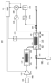
- 1 is a block diagram showing an example of the configuration of a wavelength conversion device according to a first embodiment.
- 1 is a diagram showing an example of the relationship between the wavelengths (or frequencies) of pump light, WDM signal light, and converted light of the WDM signal light;
- 1 is a graph showing an example of a change in wavelength conversion band with respect to a change in operating temperature of an optical parametric amplifier (OPA) module.
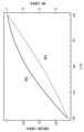
- 13 is a graph showing an example of changes in intensity (left vertical axis) and slope (right vertical axis) with respect to temperature change for light of a specific wavelength when the temperature of a wavelength conversion device changes while the pumping light power is constant.
- FIG. 11 is a block diagram showing an example of the configuration of a wavelength conversion device according to a second embodiment.
- oxide-based compounds such as lithium niobate (LN: LiNbO3 ) are promising materials because they have higher second-order nonlinear optical and electro-optic constants than other materials.
- An example of an optical device that utilizes the high nonlinearity of LN is a wavelength conversion element that utilizes second harmonic generation (SHG), difference frequency generation (DFG), and/or sum frequency generation (SFG) using periodically poled lithium niobate (PPLN).
- SHG second harmonic generation
- DFG difference frequency generation
- FSG sum frequency generation
- the converted light after wavelength conversion has a phase conjugate relationship with the signal light, making it possible to compensate for signal distortion.
- the signal light before conversion to phase conjugate light may suffer from dispersion in the optical transmission path (e.g., optical fiber) and nonlinear signal distortion due to nonlinear optical effects in the optical fiber.
- the converted signal light may suffer from dispersion and nonlinear signal distortion in the optical transmission path through which it propagates after conversion that is opposite to that before conversion.
- the dispersion and nonlinear signal distortion that occur in the signal light before conversion can be offset and reduced by the inverse dispersion and nonlinear signal distortion that occur after conversion.
- wavelength conversion technology is positioned as one of the technologies that can reduce dispersion and nonlinear signal distortion.
- an amplifier for the signal light can be constructed by transferring energy from the pump light power to the signal light.
- a phase-sensitive amplifier which has amplification characteristics according to the phase relationship between the pump light and the signal light, is expected to be a technology that enables optical amplification with low noise.
- optical waveguide devices are effective.
- the wavelength conversion efficiency is proportional to the power density of the light propagating through the nonlinear optical medium, and by forming a waveguide structure, it is possible to confine the light within a limited range.
- ridge-type optical waveguides which have features such as high optical damage resistance, long-term reliability, and easy device design, are being considered because the bulk properties of the crystal can be used as is.
- a ridge-type optical waveguide for example, has a core formed on a base substrate according to a waveguide pattern, and has a step-type refractive index distribution (see, for example, Non-Patent Document 1). Note that a ridge-type optical waveguide can operate even if the top and sides of the core are air layers (i.e., the refractive index is 1).
- the nonlinear optical medium may also be provided with a periodically poled structure (hereinafter abbreviated as "periodically poled structure”) for quasi-phase matching.
- a periodically poled structure for example, the crystal orientation is inverted for each coherence length between the fundamental wave and the wave obtained by wavelength conversion of the fundamental wave, and the sign of the nonlinear constant is inverted, making it possible to gradually or stepwise compensate for the amount of phase mismatch.
- a nonlinear optical medium having a periodically poled structure has great practical value in that it can perform a wide range of wavelength conversion from the mid-infrared range to the visible range without using a special nonlinear optical crystal.
- nonlinear optical materials have a refractive index that is temperature dependent, the pseudo-phase matching condition in second-order nonlinear optical elements may no longer be satisfied due to changes in the temperature of the nonlinear optical material. Therefore, second-order nonlinear optical elements can be controlled so that the temperature is kept constant.
- a temperature sensor such as a thermistor or thermocouple is placed on or near the second-order nonlinear optical element, and its resistance value, etc. is monitored.
- the temperature of the second-order nonlinear optical element can be kept constant by feedback controlling a temperature regulator such as a heater or Peltier element so that the difference between the monitored result and the target value is minimized.
- a mechanism that controls a temperature regulator to keep the monitored value by a temperature sensor constant may not be sufficient to precisely stabilize the operation of a second-order nonlinear optical element.
- the temperature that can be monitored by a temperature sensor such as a thermistor or thermocouple is the average temperature of the entire second-order nonlinear optical element, not the temperature of a localized part (e.g., an optical waveguide) that produces a nonlinear optical effect.
- a second-order nonlinear optical element having a ridge-type optical waveguide can operate even when there is an air layer on the top and sides of the core, and therefore can be affected by changes in environmental temperature (e.g., outside air temperature) depending on the area of the part in contact with the air layer.
- the operating point of the second-order nonlinear optical element may shift from the intended operating point in response to changes in the environmental temperature.
- the optical waveguide may generate heat due to optical absorption of the pump light incident on the optical waveguide.
- monitoring accuracy may be reduced when using a temperature sensor installed in or near the nonlinear optical element. This reduced monitoring accuracy may prevent the desired operating conditions that allow the nonlinear optical element to operate stably from being met.
- Patent Document 1 describes a method of separating two wavelengths of light generated by parametric fluorescence in a wavelength converter, and controlling the temperature of the wavelength converter based on the difference in light intensity of the two separated wavelengths.
- the following is a non-limiting example of a wavelength conversion device that includes a wavelength converter using a nonlinear optical medium and is capable of performing wavelength conversion, phase conjugation, and parametric amplification of the converted light by utilizing parametric fluorescence from the nonlinear optical medium.
- Fig. 1 is a block diagram showing an example of the configuration of a wavelength conversion device 10 according to the first embodiment.
- the wavelength conversion device 10 shown in Fig. 1 illustratively includes a pumping light source 101, an erbium-doped optical fiber amplifier (EDFA) 102, a first wavelength converter 103, and a second wavelength converter 104.
- EDFA erbium-doped optical fiber amplifier
- the first wavelength converter 103 generates the second harmonic of the pump light incident from the EDFA 102, i.e., light with a frequency that is twice the frequency of the pump light (in other words, 1/2 the wavelength of the pump light), by, for example, SHG, which is one of the nonlinear optical effects.
- SHG the light equivalent to the second harmonic
- SH light the light equivalent to the second harmonic
- the first wavelength converter 103 that generates the SH light may be referred to as an SHG module 103, and illustratively includes a first spatial optical system 131, a first PPLN waveguide 132, and a second spatial optical system 133.
- the first spatial optical system 131 spatially guides the pump light incident from the EDFA 102 to the input port of the first wavelength converter 103 to the first PPLN waveguide 132.
- the first PPLN waveguide 132 is an example of a second-order nonlinear optical element that uses a nonlinear optical medium with a periodically poled structure, and generates SH light in response to the pump light by SHG as described above.
- the second spatial optical system 133 spatially guides the SH light generated in the first PPLN waveguide 132 to the output port of the first wavelength converter 103.
- the output port of the SHG module 103 is illustratively connected to the first input port of the second wavelength converter 104, and the SH light output from the SHG module 103 is input to the second wavelength converter 104.
- the second wavelength converter 104 can operate, for example, as an OPA that uses parametric fluorescence, which is one of the nonlinear optical effects, and amplifies the signal light (e.g., WDM signal light) input through the second input port by the SH light input through the first input port.
- OPA optical photoelectron emission detector
- the second wavelength converter 104 functioning as an OPA may be referred to as an OPA module 104.
- the OPA module 104 illustratively includes a third spatial optical system 141, a first dichroic mirror 142, a second PPLN waveguide 143, a fourth spatial optical system 144, and a second dichroic mirror 145.
- the third spatial optical system 141 for example, combines the SH light input from the SHG module 103 to the first input port and the signal light input to the second input port, and spatially guides the combined light to the second PPLN waveguide 143.
- the signal light passes through the first dichroic mirror 142 and is coupled to the second PPLN waveguide 143, and the SH light is reflected by the first dichroic mirror 142 and is coupled to the second PPLN waveguide 143. Therefore, the spatial optical system 141 and the dichroic mirror 142 may be understood to constitute, for example, a "dichroic mirror type multiplexer.”
- the second PPLN waveguide 143 is an example of a second-order nonlinear optical element using a nonlinear optical medium with a periodically poled structure.
- the periodically poled structure in the second PPLN waveguide 143 illustratively satisfies a pseudo-phase matching condition between the input signal light and SH light and the output converted light. Therefore, the second PPLN waveguide 143 is capable of parametrically amplifying the signal light by using the SH light as the pump light, for example.
- the fourth spatial optical system 144 outputs the amplified signal light from the output light of the second PPLN waveguide 143 to the optical branching coupler 106.
- the amplified signal light passes through the second dichroic mirror 145 and is output to the optical branching coupler 106, and the SH light is reflected by the second dichroic mirror 145 and emitted to the outside of the OPA module 104. Therefore, the spatial optical system 144 and the dichroic mirror 145 may be understood to constitute, for example, a "dichroic mirror type splitter.”
- the OPA module 104 is thermally coupled to the TEC 105, and for example, the controller 111 can control the TEC 105 to control the temperature of the OPA module 104.
- a nonlinear optical medium such as LiNbO3 , LiTaO3 , LiNb (x) Ta (1-x) O3 (0 ⁇ x ⁇ 1), or any of these containing at least one type selected from the group consisting of Mg, Zn, Sc, and In as an additive may be used.
- the optical branching coupler 106 is illustratively a tap with a branching ratio of approximately 1/100 to 1/10, and branches off a portion of the output light from the OPA module 104 (e.g., approximately 1% to 10% of the optical intensity) and outputs it to the wavelength separation filter 107.
- the remaining light intensity is output as output light from the OPA module 104.
- the output light from the OPA module 104 may include, for example, amplified signal light, converted light of the signal light, and amplified spontaneous emission (ASE) light, which will be described later.
- ASE amplified spontaneous emission
- the wavelength separation filter 107 is, for example, a bandpass filter (BPF) type optical filter that transmits light of a specific wavelength in the wavelength band of the branched light from the optical branching coupler 106 to the light intensity detector 108 as an example of monitor light, and blocks light of other wavelengths.
- BPF bandpass filter
- the transmission bandwidth of the wavelength separation filter 107 is, for example, about 1 nm. However, this is not limited to this, and the transmission bandwidth of the wavelength separation filter 107 is not limited as long as the filter has a characteristic in which the amount of light changes in the output in response to the oscillation of the central transmission wavelength, which will be described later.
- the wavelength separation filter 107 is, as a non-limiting example, a fiber Bragg grating (FBG) type optical filter, and its central transmission wavelength can be electrically tunable.
- the wavelength separation filter 107 can periodically change the central transmission wavelength (in other words, vibrate according to the frequency of the AC signal) by an AC signal supplied from the AC signal source 110.
- the light intensity detector 108 detects, for example, the intensity of light transmitted through the wavelength separation filter 107.
- the central transmission wavelength of the wavelength separation filter 107 is vibrated by an AC signal, the amount of light transmitted through the wavelength separation filter 107 periodically varies in response to the vibration.
- the monitor light output from the wavelength separation filter 107 is frequency modulated by the AC signal. Therefore, a modulated signal component corresponding to the frequency of the AC signal appears in the output (e.g., a DC voltage signal) of the light intensity detector 108.
- the multiplier 109 synchronously detects the modulated signal component in the output of the optical intensity detector 108 by multiplying the output of the optical intensity detector 108 by a signal synchronized with the AC signal of the AC signal source 110.
- the multiplier 109 performs lock-in detection (or first-order differential detection) of the output of the optical intensity detector 108 using a reference signal with a frequency that is one time the frequency of the AC signal supplied to the wavelength separation filter 107.
- the modulated signal component is demodulated by this lock-in detection, and a differential signal equivalent to the first derivative of the intensity change, in other words, a signal indicating the slope of the intensity change, is obtained. Therefore, the multiplier 109 may be understood to correspond, for example, to a "differential signal generator” that generates a differential signal equivalent to the first derivative of the intensity change, or a “slope detector” that detects the slope of the intensity change.
- the AC signal source 110 exemplarily supplies an AC signal, which is an example of a periodic signal that periodically changes the central transmission wavelength of the wavelength separation filter 107 as described above, to the wavelength separation filter 107.
- the frequency of the AC signal may be selected, for example, based on the response characteristics in lock-in detection, which will be described later, and is exemplarily a frequency on the order of 10 kHz.
- the light intensity detector 108, multiplier 109, and AC signal source 110 described above may be understood to constitute a non-limiting example of a "detection circuit" that detects the light intensity and the slope of the change in light intensity described above.
- the controller 111 is an example of a control circuit, and for example, controls the temperature of the TEC 105 and the amplification gain of the EDFA 102 individually based on the light intensity obtained by the light intensity detector 108 and the slope of the light intensity change obtained by the multiplier 109.
- "Individually control” may be understood to include a situation in which either the temperature of the TEC 105 or the amplification gain of the EDFA 102 is the object of control, and a situation in which both are the object of control.
- the controller 111 individually controls the temperature of the TEC 105 and the amplification gain of the EDFA 102 to keep the intensity and the slope of the intensity change constant, in other words, to minimize the changes in the intensity and the slope.
- the temperature of the OPA module 104 is controlled in response to the temperature control of the TEC 105, and the power of the pump light input to the SHG module 103 is controlled in response to the amplification gain control of the EDFA 102. Therefore, the SH light power input to the OPA module 104 is controlled in response to the amplification gain control of the EDFA 102.
- PID control Proportional-Integral-Differential control
- PID control Proportional-Integral-Differential control
- the pump light output from the pump light source 101 is subjected to power control by the EDFA 102 and then input to the SHG module 103.
- SH light of the pump light is generated by SHG in the first PPLN waveguide 132.
- the SH light of the pump light is input to the OPA module 104.
- the converted light generated by the PPLN waveguide 143 is output to a dichroic mirror type splitter together with the WDM signal into which the pump light is multiplexed.
- the pump light is split from the output light of the PPLN waveguide 143, and the remaining light (e.g., amplified WDM signal light + converted light of the WDM signal light + ASE light) is output to the optical branching coupler 106 as the output light of the OPA module 104.
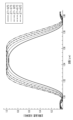
- Figure 3 is a graph showing an example of the change in wavelength conversion band with respect to the change in operating temperature of the OPA module 104.
- a method of controlling the operating temperature of the OPA module 104 by monitoring the entire band of the converted light may be considered, but this may increase the number of parts and complicate control. Also, if the power of the signal light input to the OPA module 104 fluctuates, the intensity of the converted light will also fluctuate accordingly, so control may become even more complicated if the OPA module 104 is assumed to be input with light from outside.
- the characteristics of the PPLN waveguide 143 are utilized to control the operating temperature of the OPA module 104.
- light in a wavelength region having a specific bandwidth converted from the excitation light by parametric fluorescence is used as the monitor light.
- the spectral shape of the converted light band can be controlled. For example, as shown in FIG. 2B, when the wavelength band of the input WDM signal light is 1528-1544 nm, the WDM signal light is wavelength-converted to converted light of the wavelength band 1546-1562 nm.
- the central transmission wavelength ( ⁇ BPF ) of the wavelength separation filter 107 may be set to a wavelength that does not overlap with either the wavelength bands 1528-1544 nm or 1546-1562 nm and is close to the converted light band 1546-1562 nm, for example, a wavelength of 1563 nm on the long wavelength side where the WDM signal light is not allocated.
- This wavelength of 1563 nm is a non-limiting example of a wavelength in a band where neither the WDM signal light nor the converted light is allocated.
- Figure 4 is a graph showing an example of the change in intensity and slope with respect to temperature for light of a specific wavelength (e.g., near 1545 nm) in the ASE light spectrum when the temperature of the wavelength conversion device 10 changes while the excitation light power is constant.
- reference numeral 401 indicates the change in intensity with respect to temperature change (left vertical axis)
- reference numeral 402 indicates the change in slope with respect to temperature change (right vertical axis).
- the change in intensity is normalized.
- the temperature is as shown in Figure 3.
- the controller 111 performs calculations for PID control, for example, based on the optical intensity detected by the optical intensity detector 108 and the lock-in signal (differential signal) detected by the multiplier 109.
- the controller 111 then performs feedback control of the TEC 105 and the EDFA 102 (amplification gain) individually based on the results of the calculations. This makes it possible to stabilize the optical intensity at around 0.2 dB in the converted optical band of the WDM signal light, for example.
- wavelength conversion device 10 of the first embodiment light of a specific wavelength (for example, ASE light of wavelength ⁇ BPF ) is separated by the wavelength separation filter 107 from the output light generated by parametric fluorescence in the OPA module 104.
- the optical intensity and the slope of the optical intensity change of the separated wavelength are detected by the optical intensity detector 108 and the multiplier 109, respectively, and the temperature and pumping light power of the OPA module 104 are individually controlled by the controller 111 based on the detection results.
- the spectral shape of the converted light band by parametric fluorescence can be controlled to a constant value, regardless of whether or not signal light is input to the OPA module 104. Therefore, it is possible to operate the wavelength conversion device 10 stably and for a long time under optimal or suitable operating conditions.
- the central transmission wavelength of the wavelength separation filter 107 (in other words, the wavelength ⁇ BPF of the monitor light) to a wavelength that does not overlap with the converted light band of the WDM signal light, appropriate monitoring operation can be achieved without interfering with the converted light of the WDM signal light.
- an FBG type optical filter is shown as an example of the wavelength separation filter 107 that can electrically tune the central transmission wavelength.
- a wavelength separation filter 107 with an electrically tunable central transmission wavelength may be realized by combining a narrowband BPF with an optical interferometer and modulating the optical path difference of the optical interferometer.
- a wavelength that is longer than the conversion band is selected as the wavelength of the monitor light ( ⁇ BPF ), but a wavelength that is shorter than the conversion band (e.g., 1545 nm) may be selected.
- a wavelength that is shorter than the conversion band e.g., 1545 nm
- Second Embodiment 5 is a block diagram showing a configuration example of a wavelength conversion device 10A according to a second embodiment.
- components with the same reference numerals as those already described may be understood to be the same as or similar to the already described components, unless otherwise specified.
- the wavelength conversion device 10A differs from the configuration illustrated in FIG. 1 in that it additionally includes a control light source 121 and an optical multiplexing coupler 122 provided on the input side of the OPA module 104, and that a wavelength separation filter 107A is provided instead of the wavelength separation filter 107.
- the control light source 121 is configured, for example, using a semiconductor laser, and generates control light.
- the wavelength of the control light will be described later in relation to the central transmission wavelength of the wavelength separation filter 107A.
- the optical multiplexing coupler 122 multiplexes the control light output from the control light source 121 with the signal light input to the OPA module 104.
- the wavelength separation filter 107A is a BPF type optical filter similar to the wavelength separation filter 107 in the first embodiment, and transmits light of a specific wavelength in the wavelength band of the branched light from the optical branching coupler 106 to the light intensity detector 108 as an example of monitor light.
- the transmission bandwidth of the wavelength separation filter 107A is, for example, about 1 nm, as in the first embodiment. However, this is not limited, and the transmission bandwidth of the wavelength separation filter 107A is not limited as long as the filter has a characteristic in which the light quantity changes in the output in response to the oscillation of the center frequency of the control light, which will be described later.
- the wavelength separation filter 107A does not need to have a variable central transmission wavelength, and illustratively has a fixed central transmission wavelength.
- a filter with a variable central transmission wavelength may be applied to the wavelength separation filter 107A, but the central transmission wavelength may not be variable (e.g., vibrated).
- the AC signal source 110 differs from the configuration illustrated in FIG. 1 in that it is electrically connected to the control light source 121 and supplies the control light source 121 with an AC signal, which is an example of a periodic signal that periodically changes the center frequency of the control light.
- This AC signal causes the center frequency of the control light input to the OPA module 104 via the optical multiplexing coupler 122 to oscillate.
- the wavelength conversion device 10A is configured to apply frequency modulation for lock-in detection to the control light input to the wavelength separation filter 107A.
- the multiplier 109 performs lock-in detection of the modulated signal component in the output of the optical intensity detector 108 by multiplying the output of the optical intensity detector 108 by a signal synchronized with the AC signal of the AC signal source 110.
- the light intensity detector 108, the multiplier 109, and the AC signal source 110 may be understood to constitute a non-limiting example of a "detection circuit" that detects the light intensity and the slope of the change in light intensity described above.
- the frequency of the AC signal that oscillates the center frequency of the control light may be selected based on the response characteristics in lock-in detection, as in the first embodiment, and is illustratively a frequency on the order of 10 kHz.
- the intensity of the control light output from the control light source 121 may be set to an intensity higher than the ASE light level, for example.
- the noise resistance of the light intensity detection and tilt detection can be improved more than in the first embodiment.
- the wavelength (frequency: ⁇ i ) of the control light output from the control light source 121 is, for example, the same as the central transmission wavelength of the wavelength separation filter 107 A. In other words, the wavelength of the control light matches the wavelength of the light separated by the wavelength separation filter 107 A.
- the wavelength of the control light is set to 1563 nm.
- This wavelength of 1563 nm is a non-limiting example of a wavelength that does not overlap with the converted light band of the WDM signal light and is deviated from the converted light band to the long wavelength side.
- the control light that has been frequency modulated by the AC signal from the AC signal source 110 is input to the wavelength separation filter 107A via the OPA module 104 and the optical branching coupler 106.
- the wavelength separation filter 107A whose central transmission wavelength is set to the wavelength of the control light, transmits the control light input from the optical branching coupler 106 to the optical intensity detector 108, which detects the intensity of the control light.
- the slope of the change in intensity of the control light is detected by lock-in detection using the multiplier 109 and the AC signal source 110.
- the controller 111 individually controls (e.g., PID control) the excitation light power of the excitation light source 101 and the temperature of the OPA module 104 based on the detected intensity of the control light and the slope of the intensity change.
- PID control e.g., PID control
- This control keeps the spectral shape of the converted light band constant, or minimizes changes in the spectral shape.
- the light intensity in the converted light band can be stabilized to about 0.2 dB.
- the wavelength of the control light matches the central transmission wavelength of the wavelength separation filter 107A, but the wavelength of the control light may not match the central transmission wavelength of the wavelength separation filter 107A.
- the frequency of the control light is represented by ⁇ 1
- the frequency ⁇ i of the light converted from the control light by parametric fluorescence in the OPA module 104 is represented by the following Equation 2 using the frequency 2 ⁇ 0 of the excitation light.
- ⁇ i 2 ⁇ 0 - ⁇ 1 (2)
- the converted light with frequency ⁇ i also contains a modulated component according to the frequency modulation applied by the AC signal source 110. Therefore, the central transmission wavelength of the wavelength separation filter 107A may be set to a wavelength corresponding to the frequency ⁇ i of the converted light of the control light.
- the combination of the wavelength ⁇ CONT of the control light and the central transmission wavelength ⁇ BPF of the wavelength separation filter 107A may be either (a) or (b) below.
- ⁇ CONT 1563 nm
- ⁇ BPF 1527 nm
- ⁇ CONT 1527 nm
- ⁇ BPF 1563 nm
- the central transmission wavelength of the wavelength separation filter 107A may be set to the wavelength of the control light, or may be set to the wavelength of the light converted by the parametric fluorescence of the control light.
- the wavelength of the control light and the central transmission wavelength of the wavelength separation filter 107A may be set to either of two wavelengths corresponding to the frequencies ⁇ 1 and ⁇ i , respectively, that satisfy the above-mentioned formula 2.
- the control light included in the output light of the OPA module 104 may be cut by, for example, an optical filter provided separately on the output side of the optical branching coupler 106.
- the control light may be separated from the output light of the OPA module 104 in the WDM filter and input to the wavelength separation filter 107A.
- the pump light power is controlled by controlling the amplification gain of the EDFA 102.
- the pump light power may be controlled by, for example, output light power control for the pump light source 101 having a variable output light power, or optical attenuation control of a variable optical attenuator (VOA) provided between the EDFA 102 and the SHG module 103.
- VOA variable optical attenuator
- the EDFA 102 may be omitted.
- control for example, tracking operation
- the output optical power of the pumping light source 101 in addition to controlling the amplification gain of the EDFA 102, it is possible to expand the controllable range of the pumping light power, for example.
- control for example, tracking operation
- the response speed of the pump light source 101 or the VOA is faster than the response speed of the EDFA 102.
- both the temperature and the excitation light power are controlled, but either the temperature or the excitation light power may be controlled.
- the temperature of the OPA module 104 may be controlled.
- the object to be controlled may be the light intensity (e.g., the excitation light power).
- the spectral shape can be uniquely determined including the shift in the light intensity direction, and the control time for stabilizing the spectral shape can be shortened.
- the optical branching coupler 106 may be replaced with, for example, a WDM filter that separates the signal light or converted light from the light of the specific wavelength described above (in other words, the monitor light).
- the wavelength separation filter 107 or 107A having BPF characteristics may be realized, for example, by a combination of a long-pass filter and a short-pass filter.
- the spectral shape of the signal light in the band after conversion by parametric fluorescence is controlled to be constant.
- the spectral shape of the signal light band before conversion by parametric fluorescence may be controlled to be constant.
- a central transmission wavelength ( ⁇ BPF ) of the wavelength separation filter 107 or 107A may be set to 1527 nm, which is shorter than the signal light band of 1528 to 1544 nm. This setting makes it possible to control the "spectral shape of the signal light band" to a constant value when operating as an optical parametric amplifier.
- This disclosure is expected to be utilized, for example, in the stable operation of optical elements that utilize nonlinear optical effects, and is useful in optical communication systems, optical measurement systems, and amplification technology for optical communication in general.
Landscapes
- Physics & Mathematics (AREA)
- Nonlinear Science (AREA)
- General Physics & Mathematics (AREA)
- Optics & Photonics (AREA)
- Optical Modulation, Optical Deflection, Nonlinear Optics, Optical Demodulation, Optical Logic Elements (AREA)
Abstract
本開示の波長変換装置(10)は、非線形光学媒質(143)を用いた波長変換器(104)と、非線形光学媒質(143)への励起光の入力に応じてパラメトリック蛍光により波長変換器(104)において発生した出力光の一部を分離する波長分離フィルタ(107)と、波長分離フィルタ(107)によって分離された光の強度と強度の変化の傾きとを検出する検出回路(108、109、110)と、検出された強度と傾きとに基づいて、励起光の強度および波長変換器(104)の温度を個別に制御する制御回路(111)と、を備える。
Description
本開示は、波長変換装置および制御方法に関する。
非線形光学媒質による差周波発生(DFG)を利用した波長変換技術が知られる。DFGを利用した波長変換技術によれば、例えば、光ファイバ通信において使用される波長帯の光を一括で別の波長帯の光に変換できる。
そのため、このような波長変換技術は、例えば、波長分割多重(WDM)方式における光のルーティング、または光ルーティングにおける波長の衝突回避といった光ルーティングに関する技術に適用可能である。したがって、波長変換技術は、大容量通信光ネットワークを構築する上で鍵となる技術の1つに位置づけられる。
T. Umeki, O. Tadanaga, and M. Asobe,‘Highly Efficient Wavelength Converter Using Direct-Bonded PPZnLN Ridge Waveguide,’2010年 IEEE Journal of Quantum Electronics, Vol. 46, No. 8, pp. 1206-1213
従来の波長変換技術においては、非線形光学媒質を用いた波長変換装置を安定的に動作させるための制御に関して改善の余地がある。
本開示の非限定的な目的の1つは、非線形光学媒質を用いた波長変換装置を安定的に動作させるための制御を簡易化できるようにすることにある。
そのため、本開示の一態様に係る波長変換装置は、非線形光学媒質を用いた波長変換器と、前記非線形光学媒質への励起光の入力に応じてパラメトリック蛍光により前記波長変換器において発生した出力光の一部を分離する波長分離フィルタと、前記波長分離フィルタによって分離された光の強度と前記強度の変化の傾きとを検出する検出回路と、前記強度と前記傾きとに基づいて、前記励起光の強度および前記波長変換器の温度を個別に制御する制御回路と、を備える。
また、本開示の一態様に係る制御方法は、非線形光学媒質を用いた波長変換器への励起光の入力に応じてパラメトリック蛍光により前記波長変換器において発生した出力光の一部を波長分離フィルタによって分離すること、前記波長分離フィルタによって分離された光の強度と前記強度の変化の傾きとを検出回路によって検出すること、および、検出した前記強度と前記傾きとに基づいて、前記励起光の強度および前記波長変換器の温度を制御回路によって個別に制御すること、を含む。
以下、図面を参照しながら実施形態について詳細に説明する。なお、冗長な説明を避けて説明の簡易化および明瞭化を図る目的で、図面において、同一の番号を付した要素または部分は、特に断らない限り、同一または同様の要素または部分を指す。
[概要]
光通信における光信号波長変換、光変調、光計測、または光加工、医療、生物工学などの分野に適用可能であり、紫外域-可視域-赤外域-テラヘルツ域にわたるコヒーレント光の発生および変調のために、非線形光学デバイスおよび電気光学デバイスの開発が進められている。
光通信における光信号波長変換、光変調、光計測、または光加工、医療、生物工学などの分野に適用可能であり、紫外域-可視域-赤外域-テラヘルツ域にわたるコヒーレント光の発生および変調のために、非線形光学デバイスおよび電気光学デバイスの開発が進められている。
このような光デバイスに用いられる非線形光学媒質および電気光学媒質の例としては種々の材料が研究開発されている。例えば、ニオブ酸リチウム(LN:LiNbO3)のような酸化物系化合物は、2次非線形光学定数および電気光学定数が他の材料よりも高いため有望な材料である。
LNの高非線形性を利用した光デバイスの一例として、周期的に分極反転されたニオブ酸リチウム(PPLN)による第二高調波発生(SHG)、差周波発生(DFG)、および/または、和周波発生(SFG)を利用した波長変換素子が挙げられる。
DFGを利用した波長変換では、波長変換後の変換光が信号光に対して位相共役光の関係になることを用いて、信号歪みの補償を行うことができる。例えば、位相共役光への変換前の信号光には、光伝送路(例えば、光ファイバ)において分散と、光ファイバ中の非線形光学効果による非線形信号歪みとが生じ得る。分散および信号歪みの生じた信号光を位相共役光へ変換した場合、変換後の信号光には、変換後に伝搬する光伝送路において変換前とは逆の分散および非線形信号歪みが生じ得る。
したがって、例えば、光伝送路のおよそ中間地点において信号光を位相共役光に変換することで、変換前の信号光に生じた分散および非線形信号歪みは、それぞれ、変換後において生じる逆の分散および非線形信号歪みによって相殺され低減され得る。このように、波長変換技術は、分散および非線形信号歪みを低減可能な技術の1つに位置づけられる。
ところで、波長変換効率の優れた波長変換素子を位相共役光への波長変換に用いた場合、励起光パワーから信号光へのエネルギーの移行により、光パラメトリック増幅と呼ばれる、信号光の増幅器を構成できる。例えば、励起光と信号光との間の位相関係に応じた増幅特性を有する位相感応増幅器は、低雑音での光増幅が可能な技術として期待される。
PPLNにおいて波長変換効率の向上を図るには、光導波路型のデバイスが有効である。その理由の1つは、非線形光学媒質を伝搬する光のパワー密度に波長変換効率が比例し、導波路構造を形成することで、限られた範囲に光を閉じ込めることが可能なためである。
したがって、非線形光学媒質を用いた種々の光導波路が検討される。例えば、結晶のバルクの特性をそのまま利用できるという理由から、高光損傷耐性、長期信頼性、またはデバイス設計が容易といった特徴を有するリッジ型の光導波路が検討される。
リッジ型光導波路は、例示的に、ベース基板上に導波路パターンに応じて形成されたコアを有し、かつ、ステップ型の屈折率分布を有する(例えば、非特許文献1を参照)。なお、リッジ型光導波路は、コアの上部および側部が空気層(すなわち、屈折率が1)であっても動作可能である。
また、非線形光学媒質には、擬似位相整合のために周期的に分極反転された構造(以下「周期分極反転構造」と略称する)が設けられてよい。周期分極反転構造では、例えば、基本波と基本波を波長変換した波とのコヒーレンス長ごとに結晶方位を反転し、非線形定数の符号を逆転することにより、位相不整合量を漸次的または段階的に補償することが可能である。周期分極反転構造を有する非線形光学媒質は、例えば、特殊な非線形光学結晶を用いずに中赤外域から可視域まで幅広い波長変換が行えるという点において実用的な価値が高い。
一方、非線形光学材料は温度依存性の屈折率を有するため、2次非線形光学素子において擬似位相整合条件が、非線形光学材料の温度変化によって満たされなくなることがある。そのため、2次非線形光学素子は、温度が一定に保たれるように制御され得る。
例えば、2次非線形光学素子またはその近傍にサーミスタ、熱電対といった測温体を設け、その抵抗値等をモニタする。このモニタ結果と目標値との差分が最小となるように、ヒータ、ペルチェ素子といった温度調節器をフィードバック制御することにより、2次非線形光学素子の温度を一定に保つことができる。
しかしながら、測温体によるモニタ値を一定にするように温度調節器を制御する機構では、2次非線形光学素子の動作を精密に安定化するためには不十分な場合がある。例えば、サーミスタ、熱電対といった測温体によってモニタすることが可能な温度は、2次非線形光学素子の全体の平均的な温度であり、非線形光学効果をもたらす局所的な部分(例えば、光導波路)の温度ではない。
そのため、測温体による温度モニタでは、2次非線形光学素子を動作させる温度を安定動作が可能な所期の温度に制御することが難しい場合がある。例えば、リッジ型光導波路を有する2次非線形光学素子では、既述のとおり、コアの上部および側部が空気層である場合においても動作可能であるため、空気層に接する部分の面積に応じて環境温度(例えば、外気温度)の変化の影響を受け得る。
よって、2次非線形光学素子またはその近傍に設置した測温体によるモニタ温度が一定となるように当該素子の温度を制御した場合、環境温度の変化に応じて2次非線形光学素子の動作点が所期の動作点からシフトし得る。
また、光パラメトリック増幅による変換効率または利得を向上するために、光導波路に入射する励起光のパワーを増加した場合、光導波路内に入射した励起光の光吸収によって光導波路が発熱し得る。
この発熱は、光導波路という局所的な部分であるため、非線形光学素子またはその近傍に設置した測温体を用いたモニタではモニタ精度が低下し得る。モニタ精度の低下によって、非線形光学素子を安定的に動作させることが可能な所期の動作条件を満たすことが妨げられ得る。
測温体を用いた温度制御の代替例として、特許文献1に記載された技術の適用が検討される。特許文献1には、波長変換器においてパラメトリック蛍光により発生した2つ波長の光を分離し、分離した2つ波長の光強度の差分に基づいて波長変換器の温度を制御することが記載される。
しかしながら、この技術では、波長変換器の温度制御のために複数波長の光をそれぞれ光分岐カプラおよび光帯域通過フィルタを用いて分離するため、温度制御のために使用する光学部品点数が増加し、制御系の構成および動作が複雑化し得る。
そこで、以下に説明する幾つかの非限定的な実施形態では、非線形光学媒質を用いた波長変換器の安定的な動作のための制御を簡易化することが可能な技術について説明する。
例えば、非線形光学媒質を用いた波長変換器を含み、非線形光学媒質によるパラメトリック蛍光を利用して、波長変換および位相共役と変換光のパラメトリック増幅とを行うことが可能な波長変換装置の非限定的な例が以下に示される。
[第1の実施形態]
図1は、第1の実施形態に係る波長変換装置10の構成例を示すブロック図である。図1に示す波長変換装置10は、例示的に、励起光源101、エルビウム添加光ファイバ増幅器(EDFA)102、第1の波長変換器103、および、第2の波長変換器104を備える。
図1は、第1の実施形態に係る波長変換装置10の構成例を示すブロック図である。図1に示す波長変換装置10は、例示的に、励起光源101、エルビウム添加光ファイバ増幅器(EDFA)102、第1の波長変換器103、および、第2の波長変換器104を備える。
EDFA102は、励起光源101の出力に光学的に接続され、第1の波長変換器103は、EDFA102の出力に光学的に接続される。第2の波長変換器104は、例示的に、2つの入力ポートの1つが第1の波長変換器103の出力と光学的に接続される。
また、波長変換装置10は、例えば、温度調節器の一例である熱電クーラ(TEC)105と、第2の波長変換器104の出力に光学的に接続された光分岐カプラ106とを備える。光分岐カプラ106は、「タップ」と称されてもよい。さらに、波長変換装置10は、例えば、光分岐カプラ106の分岐出力の一方に光学的に接続された波長分離フィルタ107と、波長分離フィルタ107の出力に光学的に接続された光強度検出器108とを備える。
また、波長変換装置10は、例えば、光強度検出器108の出力に電気的に接続された乗算器109、乗算器109と波長分離フィルタ107とのそれぞれに電気的に接続された交流信号源110、および、制御器111を備える。制御器111は、例示的に、EDFA102、TEC105、光強度検出器108および乗算器109のそれぞれと電気的に接続される。
励起光源101は、例えば、半導体レーザによって励起光を生成し、生成した励起光をEDFA102へ出力する。EDFA102は、励起光源101から入射した励起光を増幅し、増幅した励起光を第1の波長変換器103へ出力する。EDFA102の増幅利得(別言すると、励起光のパワー)は、例えば、制御器111からの制御によって可変され得る。
第1の波長変換器103は、例えば、非線形光学効果の1つであるSHGによって、EDFA102から入射した励起光の第2高調波、すなわち、励起光の周波数を2倍にした周波数(別言すると、励起光の1/2波長)の光を発生する。なお、第2高調波に相当する光を便宜的に「SH光」と称することがある。
SH光を発生する第1の波長変換器103は、SHGモジュール103と称されてもよく、例示的に、第1の空間光学系131と、第1のPPLN導波路132と、第2の空間光学系133と、を備える。
第1の空間光学系131は、例えば、第1の波長変換器103の入力ポートにEDFA102から入射した励起光を第1のPPLN導波路132へ空間的に導く。第1のPPLN導波路132は、周期分極反転構造の非線形光学媒質を用いた2次非線形光学素子の一例であり、上述したようにSHGによって励起光に対するSH光を発生する。
第2の空間光学系133は、第1のPPLN導波路132において発生したSH光を第1の波長変換器103の出力ポートへ空間的に導く。SHGモジュール103の出力ポートは、例示的に、第2の波長変換器104の第1の入力ポートに接続されており、SHGモジュール103から出力されたSH光が第2の波長変換器104に入力される。
第2の波長変換器104は、例えば、非線形光学効果の1つであるパラメトリック蛍光を利用したOPAとして動作可能であり、第2の入力ポートを通じて入力された信号光(例えばWDM信号光)を、第1の入力ポートを通じて入力されたSH光によって増幅する。
OPAとして機能する第2の波長変換器104は、OPAモジュール104と称されてもよい。OPAモジュール104は、例示的に、第3の空間光学系141と、第1のダイクロイックミラー142と、第2のPPLN導波路143と、第4の空間光学系144と、第2のダイクロイックミラー145と、を備える。
第3の空間光学系141は、例えば、第1の入力ポートにSHGモジュール103から入力されたSH光と、第2の入力ポートに入力された信号光と、を合波して第2のPPLN導波路143へ空間的に導く。
例示的に、信号光は、第1のダイクロイックミラー142を透過して第2のPPLN導波路143に結合し、SH光は、第1のダイクロイックミラー142において反射されて第2のPPLN導波路143に結合する。そのため、空間光学系141およびダイクロイックミラー142は、例えば、「ダイクロイックミラー型合波器」を構成すると理解されてもよい。
第2のPPLN導波路143は、周期分極反転構造の非線形光学媒質を用いた2次非線形光学素子の一例である。第2のPPLN導波路143における周期分極反転構造は、例示的に、入力される信号光およびSH光と出力する変換光との間において擬似位相整合条件を満たす。したがって、第2のPPLN導波路143は、例えば、信号光を励起光としてのSH光によりパラメトリック増幅することが可能である。
第4の空間光学系144は、第2のPPLN導波路143の出力光のうち、増幅された信号光を光分岐カプラ106へ出力する。例示的に、増幅された信号光は、第2のダイクロイックミラー145を透過して光分岐カプラ106へ出力され、SH光は、第2のダイクロイックミラー145によって反射されてOPAモジュール104の外部へ放射される。そのため、空間光学系144およびダイクロイックミラー145は、例えば、「ダイクロイックミラー型分波器」を構成すると理解されてもよい。
OPAモジュール104には、TEC105が熱的に結合されており、例えば、制御器111がTEC105を制御することにより、OPAモジュール104の温度を制御することが可能である。
なお、SHGモジュール103およびOPAモジュール104のそれぞれには、非限定的な一例として、LiNbO3、LiTaO3、LiNb(x)Ta(1-x)O3(0≦x≦1)、または、それらにMg、Zn、Sc、Inからなる群から選ばれた少なくとも一種を添加物として含有する非線形光学媒質が用いられよい。
光分岐カプラ106は、例示的に、1/100~1/10程度の分岐比を有するタップであり、OPAモジュール104の出力光の一部(例えば、1%~10%程度の光強度)を分岐して波長分離フィルタ107へ出力する。
残りの光強度の光は、OPAモジュール104の出力光として出力される。なお、OPAモジュール104の出力光には、例えば、増幅された信号光、当該信号光の変換光、および、後述の自然放射増幅光(ASE光)が含まれ得る。
波長分離フィルタ107は、例えば、光分岐カプラ106からの分岐光の波長帯域における特定波長の光をモニタ光の一例として光強度検出器108へ透過し、その他の波長の光は遮断するバンドパスフィルタ(BPF)タイプの光学フィルタである。
波長分離フィルタ107の透過帯域幅は、例示的に、1nm程度である。ただし、これに限られず、後述する中心透過波長の振動に応じて出力に光量変化が現れる特性を有するフィルタであれば波長分離フィルタ107の透過帯域幅は制限されない。
本例において、波長分離フィルタ107は、非限定的な一例として、ファイバブラッググレーティング(FBG)タイプの光学フィルタであり、その中心透過波長を電気的に可変できる。例えば、波長分離フィルタ107は、交流信号源110から供給される交流信号によって中心透過波長を周期的に変化(別言すると、交流信号の周波数に応じて振動)させることが可能である。
光強度検出器108は、例えば、波長分離フィルタ107を透過した光の強度を検出する。ここで、上述したように波長分離フィルタ107の中心透過波長を交流信号によって振動させた場合、その振動に応じて波長分離フィルタ107を透過する光量が周期的に変動する。
別言すると、波長分離フィルタ107から出力されるモニタ光が、交流信号によって周波数変調される。したがって、光強度検出器108の出力(例えば、直流電圧信号)には、交流信号の周波数に応じた変調信号成分が現れる。
乗算器109は、光強度検出器108の出力に、交流信号源110の交流信号に同期した信号を乗じることにより、光強度検出器108の出力における変調信号成分を同期検波する。別言すると、乗算器109は、波長分離フィルタ107に供給される交流信号の周波数の1倍の参照信号によって光強度検出器108の出力をロックイン検波(または1階微分検波)する。
このロックイン検波によって変調信号成分が復調されて、強度変化の1階微分に相当する微分信号、別言すると、強度変化の傾きを示す信号が得られる。そのため、乗算器109は、例示的に、強度変化の1階微分に相当する微分信号を生成する「微分信号生成器」、または、強度変化の傾きを検出する「傾き検出器」に相当すると理解されてもよい。
交流信号源110は、例示的に、上述したように波長分離フィルタ107の中心透過波長を周期的に変化させる周期信号の一例である交流信号を波長分離フィルタ107に供給する。交流信号の周波数は、例えば、後述するロックイン検波での応答特性に基づいて選択されてよく、例示的に、10kHzオーダの周波数である。
なお、上述した光強度検出器108、乗算器109、および、交流信号源110は、上述した光強度と光強度変化の傾きとを検出する「検出回路」の非限定的な一例を構成すると理解されてよい。
制御器111は、制御回路の一例であり、例示的に、光強度検出器108によって得られる光強度と乗算器109によって得られる光強度変化の傾きとに基づいて、TEC105の温度およびEDFA102の増幅利得を個別に制御する。「個別に制御する」とは、TEC105の温度およびEDFA102の増幅利得の一方が制御対象である態様と双方が制御対象である態様とを含む表現であると理解されてよい。
例えば、制御器111は、TEC105の温度およびEDFA102の増幅利得を個別に制御することにより、強度および強度変化の傾きをそれぞれ一定にする、別言すると、強度および傾きそれぞれの変化を最小化する。
なお、TEC105の温度制御に応じてOPAモジュール104の温度が制御され、EDFA102の増幅利得制御に応じてSHGモジュール103へ入力される励起光のパワーが制御される。したがって、EDFA102の増幅利得制御に応じてOPAモジュール104に入力されるSH光パワーが制御される。制御器111による制御には、例えば、PID制御(Proportional-Integral-Differential control)が適用されてよい。
(動作例)
次に、上述した波長変換装置10の動作例を説明する。波長変換装置10において、励起光源101から出力された励起光は、EDFA102によるパワー制御を受けた後、SHGモジュール103に入力される。SHGモジュール103では、第1のPPLN導波路132においてSHGにより励起光のSH光が生成される。励起光のSH光は、OPAモジュール104に入力される。
次に、上述した波長変換装置10の動作例を説明する。波長変換装置10において、励起光源101から出力された励起光は、EDFA102によるパワー制御を受けた後、SHGモジュール103に入力される。SHGモジュール103では、第1のPPLN導波路132においてSHGにより励起光のSH光が生成される。励起光のSH光は、OPAモジュール104に入力される。
OPAモジュール104には、例えば、SH光と、入力信号光の一例としてのWDM信号光とが入力される。OPAモジュール104において、WDM信号光と励起光とがダイクロイックミラー型合波器によって合波され、PPLN導波路143に入射する。
PPLN導波路143は、例えば、DFGによりWDM信号光の変換光を生成する。ここで、励起光の周波数を2ω0、WDM信号光を構成する何れかの波長に対応する周波数をωsとそれぞれ表した場合、PPLN導波路143中のDFGにより、周波数2ω0-ωsの変換光が生成される。光位相としては、励起光の位相をΦp、信号光の位相をΦsとそれぞれ表した場合、DFGにより、励起光の位相Φpを基準として、位相がΦp-Φsである、信号光の位相共役光が生成される。
励起光の2倍の波長(周波数:ω0)を基本波波長と定義した場合、WDM信号光に含まれる複数波長の信号光は、例えば、基本波波長を中心波長軸として折り返した波長の変換光として生成される。変換光の生成と共に、励起光からWDM信号光にエネルギーが移行するため、WDM信号光が増幅される。
PPLN導波路143により生成された変換光は、励起光が合波されたWDM信号と共にダイクロイックミラー型分波器に出力される。ダイクロイックミラー型分波器において、PPLN導波路143の出力光から励起光が分波され、残りの光(例えば、増幅されたWDM信号光+WDM信号光の変換光+ASE光)がOPAモジュール104の出力光として光分岐カプラ106へ出力される。
光分岐カプラ106は、OPAモジュール104の出力光の僅かな一部を分岐して波長分離フィルタ107へ出力し、残りの出力光を波長変換装置10の出力光として出力する。なお、光分岐カプラ106の出力から「WDM信号の変換光」が取り出される場合、波長変換装置10は、波長変換器および位相共役変換器として機能する。これに対し、光分岐カプラ106の出力から「増幅されたWDM信号光」が取り出される場合、波長変換装置10は、光パラメトリック増幅器として機能する。
図2は、励起光、信号光、および、信号光の変換光の波長(または周波数)の関係の一例を示す図である。非限定的な一例として、基本波波長λ0(周波数:ω0)を1545ナノメートル(nm)、励起光波長λp(周波数:2ω0)を772.5nmとした場合の、PPLN導波路143の波長変換(帯域)について、図2(a)を用いて説明する。
なお、PPLN導波路143の長手方向の長さ(素子長)は、非限定的な一例として、42ミリメートル(mm)である。また、図2(b)は、信号光がWDM信号光であるケースについての波長変換帯域の一例を示し、その説明については後述する。
励起光および信号光がPPLN導波路143に入力された場合、PPLN導波路143のDFGにより信号光の変換光が生成される。図2(a)に示すように、信号光の波長λs(周波数:ωs)を1540nmとした場合、信号光の変換光は、励起光と信号光との差分の周波数である2ω0-ωs、つまりは波長λc=1550nmの光として生成される。波長領域において考えた場合、変換光は、基本波波長λ0を中心波長軸として信号光を折り返した形で生成される。
PPLN導波路143では、励起光、信号光、および、変換光の3波の光の間において擬似位相整合条件が満たされる。例えば、励起光、信号光、変換光の光導波路中の実効屈折率を、それぞれ、np、ns、ncと表した場合、PPLN導波路143は、以下の式1を満たす反転周期Λの分極反転構造を有する。
np/λp-ns/λs-nc/λc=1/Λ (1)
np/λp-ns/λs-nc/λc=1/Λ (1)
式1が満たされる場合、信号光の波長λsが変化しても、励起光と周波数2ω0-ωsの変換光との間では同じ変換効率が得られる。例えば、信号光波長λs(周波数:ωs)を1539nmとした場合、2ω0-ωsにより、波長1551nmの変換光が生成される。
このとき、信号光の実効屈折率nsおよび変換光の実効屈折率ncも変化するが、材料の分散により信号光の実効屈折率nsの増加分に応じて変換光の実効屈折率ncが減少する。そのため、信号光波長λsを変更した場合でも、式1を満たすことができ、波長変換帯域の広帯域化を図ることができる。
ここで、このような波長変換前後の帯域形状(別言すると、スペクトル形状)は、OPAモジュール104の動作温度が適正である場合に満たされ、動作温度が適正温度からずれた場合、帯域形状が変化し得る。温度変化の場合は、実効屈折率np、ns、ncのそれぞれが変化するため、その変化に応じて得られる波長変換帯域が変化し得る。
図3は、OPAモジュール104の動作温度の変化に対する波長変換帯域の変化の一例を示すグラフである。図3には、非限定的な一例として、波長帯の変換において使用する基準温度をΔT=0.0℃とし、基準温度から±0.1℃、および、±0.2℃の温度幅においてそれぞれ変化させた場合のグラフが示される。なお、図3では、上述した条件における波長変換帯域の光強度が正規化して示される。
WDM信号光における1波長の信号光の変換光をモニタして、OPAモジュール104の動作温度を制御する方法が検討され得るが、変換光の波長によって光強度の温度依存性が異なる。そのため、単純には温度制御における温度の上下関係(別言すると、温度の増減方向)を特定することが難しい。
変換光の全帯域をモニタして、OPAモジュール104の動作温度を制御する方法も検討され得るが、部品点数が増加して制御が複雑になり得る。また、OPAモジュール104に入力される信号光のパワーが変動した場合、その変動に応じて変換光の強度も変動するため、OPAモジュール104に対する外部からの光入力が前提では制御がさらに複雑化し得る。
そこで、本実施形態では、PPLN導波路143の特性を利用して、OPAモジュール104の動作温度を制御する。例えば、パラメトリック蛍光により励起光から変換された特定の帯域幅を有する波長領域の光をモニタ光に利用する。
パラメトリック蛍光は、信号光が入力されなくても非線形光学媒質からの自然放出光(ASE光)の存在によって、非線形光学媒質に入射した励起光が、その周波数よりも低い2つの周波数の光に変換される自発パラメトリック過程である。例えば、2次の非線形光学媒質に周波数2ω0の励起光を入射した場合、励起光は、ω1+ω2=2ω0を満たす2つの周波数ω1および周波数ω2の光に変換される。
波長分離フィルタ107は、既述のとおり、特定波長の光を透過し、その他の波長の光は遮断するBPF型の光学フィルタである。特定波長の光は、例示的に、OPAモジュール104にてパラメトリック蛍光により発生した光の帯域のうち、WDM信号光の変換光の帯域(以下「変換光帯域」と称することがある)に重ならない波長の光であってよい。代替的または追加的に、特定波長の光は、WDM信号光の帯域に重ならない波長の光であってもよい。
例えば、基本波波長を基準としてWDM信号光の変換光帯域に近接した波長を特定波長(周波数:ωBPF)に選ぶことにより、変換光帯域のスペクトル形状を制御できる。例示的に、図2(b)に示すように、入力WDM信号光の波長帯域を1528~1544nmとした場合、WDM信号光は、波長帯域1546~1562nmの変換光に波長変換される。
この場合、波長分離フィルタ107の中心透過波長(λBPF)は、波長帯域1528~1544nmおよび1546~1562nmの双方に重ならない波長であって変換光帯域1546~1562nmに近接した波長、例えばWDM信号光が配置されない長波長側の波長1563nmに設定されてよい。この波長1563nmは、WDM信号光、および、その変換光の双方が配置されない帯域における波長の非限定的な一例である。
波長分離フィルタ107の中心透過波長が上述のごとく設定された状態において、パラメトリック蛍光による光強度および光強度変化の傾きが、波長分離フィルタ107の出力光から光強度検出器108および乗算器109によって検出される。
そして、検出された光強度および光強度変化の傾きが一定になるように、励起光源101の励起光パワーとOPAモジュール104の温度とが個別に制御器111によって制御される。この制御によって、WDM信号光の変換帯域のスペクトル形状を一定に保つことができる、または、スペクトル形状の変化を最小化できる。
図4は、励起光パワーが一定の状態において波長変換装置10の温度が変化した場合のASE光スペクトルにおける特定の波長(例えば、1545nm付近)の光について、温度変化に対する強度および傾きの変化の一例を示すグラフである。図4において、符号401が温度変化に対する強度の変化(左縦軸)を示し、符号402が温度変化に対する傾きの変化(右縦軸)を示す。強度の変化は正規化されている。温度は図3に例示した状況である。
図4に例示したように、波長領域においてある程度ASE光スペクトルが広がった状態の場合、変換帯域外の特定波長のASE光スペクトルの強度および傾きは、何れも温度変化に応じて単調に増加または減少する傾向にある。一方、温度が一定の場合、励起光パワーの増加(または減少)に応じてASE光スペクトルは、そのスペクトル形状を保ったまま強度方向にシフトする傾向にある。
したがって、特定波長のASE光の強度および強度変化の傾きをそれぞれ一定にすることで、ASE光スペクトルの形状を一定にできる、または、スペクトル形状の変化を最小化できる。そこで、制御器111は、上述した強度および傾きという2つのパラメータを基に励起光パワーと温度とについて個別にフィードバック制御を行う。
例えば、制御器111は、温度制御によってASE光の強度変化の傾きを一定化した後、励起光パワー(例えば、EDFA102の増幅利得)の制御によってASE光の強度を一定化する。
制御器111においては、例えば、光強度検出器108によって検出された光強度と、乗算器109によって検出されたロックイン信号(微分信号)とを基に、PID制御のための計算を行う。そして、制御器111は、その計算結果に基づいて、TEC105およびEDFA102(増幅利得)を個別にフィードバック制御する。これにより、例えば、WDM信号光の変換光帯域において光強度を0.2dB程度に安定させることができる。
以上のように、第1の実施形態の波長変換装置10によれば、OPAモジュール104にてパラメトリック蛍光により発生した出力光から特定波長の光(例えば、波長λBPFのASE光)が波長分離フィルタ107によって分離される。分離された波長の光強度および光強度変化の傾きがそれぞれ光強度検出器108および乗算器109によって検出され、その検出結果に基づいて、OPAモジュール104の温度と励起光パワーとが制御器111によって個別に制御される。
このような動作により、OPAモジュール104に対する信号光の入力の有無に依存せずに、パラメトリック蛍光による変換光帯域のスペクトル形状を一定に制御できる。したがって、最適または好適な動作条件において波長変換装置10を安定的、長期的に動作させることが可能となる。
また、OPAモジュール104の温度と励起光パワーとの個別制御において、1波長の特定波長(例えば、λBPF)の光をモニタすればよいため、例えば、上述した制御のために使用する光学部品点数の増加を抑制できる。したがって、制御器111を含む制御系の簡易化を図ることができる。
さらに、波長分離フィルタ107の中心透過波長(別言すると、モニタ光の波長λBPF)を、WDM信号光の変換光帯域に重ならない波長に設定することで、WDM信号光の変換光に干渉せずに適切なモニタ動作を実現できる。
なお、第1の実施形態では、中心透過波長を電気的に可変できる波長分離フィルタ107の例として、FBGタイプの光学フィルタを示した。代替的に、例えば、狭帯域BPFと光干渉計とを組み合わせて光干渉計の光路差に変調を加える構成によって、中心透過波長が電気的に可変である波長分離フィルタ107が実現されてもよい。
また、上述した第1の実施形態においては、モニタ光の波長(λBPF)に変換光帯域から長波長側に外れた波長を選んだが、例示的に、変換光帯域から短波長側に外れた波長(例えば、1545nm)を選んでもよい。ただし、例えば、波長資源の利用効率向上のためにWDM信号光の帯域と変換光帯域との間に信号光を配置することが想定される場合、短波長側よりも長波長側に外れた波長をモニタ光の波長に選ぶ方が好ましいと云える。
[第2の実施形態]
図5は、第2の実施形態に係る波長変換装置10Aの構成例を示すブロック図である。図5において既述の符号と同一符号を付した構成要素は、特に断らない限り、既述の構成要素と同一若しくは同様と理解されてよい。
図5は、第2の実施形態に係る波長変換装置10Aの構成例を示すブロック図である。図5において既述の符号と同一符号を付した構成要素は、特に断らない限り、既述の構成要素と同一若しくは同様と理解されてよい。
波長変換装置10Aは、図1に例示した構成に比して、制御光源121と、OPAモジュール104の入力側に設けられた光合波カプラ122とを追加的に備え、かつ、波長分離フィルタ107に代えて波長分離フィルタ107Aが設けられる点が異なる。
制御光源121は、例えば、半導体レーザを用いて構成され、制御光を生成する。制御光の波長については波長分離フィルタ107Aの中心透過波長との関係において後述する。光合波カプラ122は、制御光源121から出力される制御光を、OPAモジュール104に入力される信号光に合波する。
波長分離フィルタ107Aは、第1の実施形態における波長分離フィルタ107と同様にBPFタイプの光学フィルタであり、光分岐カプラ106からの分岐光の波長帯域における特定波長の光をモニタ光の一例として光強度検出器108へ透過する。
波長分離フィルタ107Aの透過帯域幅は、第1の実施形態と同様に、例えば1nm程度である。ただし、これに限られず、後述する制御光の中心周波数の振動に応じて出力に光量変化が現れる特性を有するフィルタであれば波長分離フィルタ107Aの透過帯域幅は制限されない。
ここで、波長分離フィルタ107Aは、第1の実施形態とは異なり、中心透過波長が可変である必要はなく、例示的に、固定の中心透過波長を有する。代替的に、波長分離フィルタ107Aに中心透過波長が可変のフィルタを適用するが、中心透過波長は可変(例えば、振動)させないこととしてもよい。
交流信号源110は、図1に例示した構成とは異なり、制御光源121と電気的に接続されており、制御光の中心周波数を周期的に変化させる周期信号の一例である交流信号を制御光源121に供給する。この交流信号によって、光合波カプラ122を通じてOPAモジュール104に入力される制御光の中心周波数が振動する。
別言すると、波長変換装置10Aは、波長分離フィルタ107Aの透過光に対してロックイン検波のための周波数変調をかける代わりに、波長分離フィルタ107Aに入力される制御光に対してロックイン検波のための周波数変調を加える構成を有する。
そのため、第2の実施形態において、乗算器109は、光強度検出器108の出力に、交流信号源110の交流信号に同期した信号を乗じることにより、光強度検出器108の出力における変調信号成分をロックイン検波する。
なお、第2の実施形態においても、光強度検出器108、乗算器109、および、交流信号源110は、上述した光強度と光強度変化の傾きとを検出する「検出回路」の非限定的な一例を構成すると理解されてよい。
制御光の中心周波数を振動させる交流信号の周波数は、第1の実施形態と同様に、ロックイン検波での応答特性に基づいて選択されてよく、例示的に、10kHzオーダの周波数である。
制御光源121から出力される制御光の強度は、例示的に、ASE光レベルよりも高い強度に設定されてよい。制御光の強度をASE光レベルよりも高い強度に設定することで、光強度検出および傾き検出の雑音耐性を第1の実施形態よりも高めることができる。
制御光源121から出力される制御光の波長(周波数:ωi)は、例示的に、波長分離フィルタ107Aの中心透過波長と同じ波長である。別言すると、制御光の波長は、波長分離フィルタ107Aにおいて分離される光の波長と一致する。
図2を参照して非限定的な波長配置を例示すると、基本波波長λ0(周波数:ω0)が1545nmであり、波長分離フィルタ107の中心透過波長が1563nmである場合、制御光の波長は1563nmに設定される。この波長1563nmは、WDM信号光の変換光帯域に重ならない波長であって変換光帯域から長波長側に外れた波長の非限定的な一例である。
上述した構成を有する波長変換装置10Aでは、交流信号源110からの交流信号によって周波数変調を受けた制御光が、OPAモジュール104および光分岐カプラ106を経由して、波長分離フィルタ107Aに入力される。
中心透過波長が制御光の波長に設定された波長分離フィルタ107Aは、光分岐カプラ106から入力された制御光を光強度検出器108へ透過し、光強度検出器108において制御光の強度が検出される。また、制御光の強度変化の傾きが、乗算器109および交流信号源110を用いたロックイン検波によって検出される。
制御器111は、検出された制御光の強度および強度変化の傾きに基づいて、励起光源101の励起光パワーとOPAモジュール104の温度とを個別に制御(例えば、PID制御)する。この制御によって、変換光帯域のスペクトル形状が一定に保たれる、または、スペクトル形状の変化が最小化される。例えば、変換光帯域において光強度を0.2dB程度に安定させることができる。
なお、上述した第2の実施形態においては、制御光の波長が波長分離フィルタ107Aの中心透過波長と一致する例について説明したが、制御光の波長は、波長分離フィルタ107Aの中心透過波長と不一致であってもよい。
例えば、制御光の周波数をω1によって表した場合、制御光がOPAモジュール104においてパラメトリック蛍光により変換された光の周波数ωiは、励起光の周波数2ω0を使って、以下の式2によって表される。
ωi=2ω0-ω1 (2)
ωi=2ω0-ω1 (2)
この周波数ωiの変換光についても、変換前の制御光(周波数:ω1)と同じく、交流信号源110によって加えられた周波数変調に応じた変調成分が含まれる。したがって、波長分離フィルタ107Aの中心透過波長は、制御光の変換光の周波数ωiに対応する波長に設定されてもよい。
非限定的な波長配置を例示すると、基本波波長λ0(周波数:ω0)が1545nmである場合、制御光の波長λCONTおよび波長分離フィルタ107Aの中心透過波長λBPFの組み合わせは、以下の(a)および(b)の何れであってもよい。
(a)λCONT=1563nm;λBPF=1527nm
(b)λCONT=1527nm;λBPF=1563nm
(a)λCONT=1563nm;λBPF=1527nm
(b)λCONT=1527nm;λBPF=1563nm
別言すると、波長分離フィルタ107Aの中心透過波長は、制御光の波長に設定されてもよいし、制御光のパラメトリック蛍光による変換光の波長に設定されてもよい。さらに別言すれば、制御光の波長および波長分離フィルタ107Aの中心透過波長は、前掲の式2を満たす周波数ω1およびωiのそれぞれに対応する2波長の何れに設定されてもよい。
なお、OPAモジュール104の出力光に含まれる制御光は、例えば、光分岐カプラ106の出力側に個別に設けられた光学フィルタによってカットされてよい。代替的に、例えば、光分岐カプラ106をWDMフィルタに置換することによって、OPAモジュール104の出力光から制御光をWDMフィルタにおいて分離して波長分離フィルタ107Aに入力する構成としてもよい。
[各実施形態に共通の補足]
上述した各実施形態では、励起光の第2高調波(SH光)を、SHGモジュール103によって生成する構成について例示したが、SH光の波長の光を出力可能な光源を励起光源101に適用する場合には、SHGモジュール103は設けられなくてもよい。
上述した各実施形態では、励起光の第2高調波(SH光)を、SHGモジュール103によって生成する構成について例示したが、SH光の波長の光を出力可能な光源を励起光源101に適用する場合には、SHGモジュール103は設けられなくてもよい。
また、上述した各実施形態では、励起光パワーの制御がEDFA102の増幅利得制御によって行われる例を示した。代替的または追加的に、励起光パワーの制御は、例えば、出力光パワーが可変の励起光源101に対する出力光パワー制御、またはEDFA102とSHGモジュール103との間に設けた可変光減衰器(VOA)の光減衰量制御によって行われてもよい。
なお、SHGモジュール103からOPAモジュール104に入力される励起光の2倍高調波であるSH光の光パワーレンジとして、OPAの動作に十分なレンジを確保できる場合、EDFA102は省略されてもよい場合がある。
また、EDFA102の増幅利得制御に加えて、励起光源101の出力光パワー制御が可能である場合には、例えば、励起光パワーの制御可能なレンジの拡大を図ることができる。さらに、EDFA102の増幅利得制御に加えて、励起光源101の出力光パワー制御またはVOAの減衰量制御が可能である場合には、例えば、個々の応答速度に応じて制御(例えば、追従動作)が分担されてよい。
非限定的な一例として、EDFA102の応答速度よりも励起光源101またはVOAの応答速度の方が早い場合を想定する。この場合、相対的に大きな変動はEDFA102の増幅利得制御によって追従し、相対的に小さく早い変動は励起光源101に対する制御またはVOAの減衰量制御によって追従するといった制御動作の分担が可能である。
また、上述した各実施形態においては、温度と励起光パワーとの双方が制御対象であるが、温度と励起光パワーとの一方が制御対象とされてもよい。例えば、光強度(例えば、励起光パワー)が一定化、または、光強度の変動が最小化されている状況では、OPAモジュール104の温度が制御対象とされてよい。
これに対し、例えば、OPAモジュール104の温度が一定化(または、温度変動が最小化)されている状況では、制御対象が光強度(例えば、励起光パワー)とされてよい。ただし、温度と励起光パワーとの双方を制御対象とすることにより、光強度方向のシフトを含んで一意にスペクトル形状を決定できるため、スペクトル形状を安定化させるための制御時間を短縮できる。
また、各実施形態において、光分岐カプラ106は、例えば、信号光または変換光と既述の特定波長の光(別言すると、モニタ光)とを分離するWDMフィルタに置換されてもよい。BPF特性を有する波長分離フィルタ107または107Aは、例えば、ロングパスフィルタおよびショートパスフィルタの組み合わせによって実現されてもよい。
さらに、各実施形態においては、信号光のパラメトリック蛍光による変換後の帯域におけるスペクトル形状を一定に制御する例について示した。代替的に、パラメトリック蛍光による変換前の信号光帯域のスペクトル形状が一定に制御されてもよい。
図2を参照して非限定的な一例について説明すると、1528~1544nmの信号光帯域から短波長側に外れた1527nmが、波長分離フィルタ107または107Aの中心透過波長(λBPF)に設定されてもよい。この設定によれば、光パラメトリック増幅器としての動作における「信号光帯域のスペクトル形状」を一定に制御することが可能である。
以上、本開示について詳細に説明したが、本開示を通じて説明した内容に本開示の趣旨および範囲が限定されないことは当業者に明らかである。本開示は、請求の範囲の記載によって定まる本開示の趣旨および範囲を逸脱することなく修正および変更態様として実施可能である。したがって、本開示の記載は、例示的な説明を目的とし、本開示の趣旨および範囲に対して何らの制限的な意味を有さない。
本開示は、例えば、非線形光学効果を用いた光学素子の安定的な動作に活用されることが想定され、光通信システム、光計測システム、光通信用の増幅技術一般に有用である。
10、10A 波長変換装置
101 励起光源
102 エルビウム添加光ファイバ増幅器(EDFA)
103 第1の波長変換器(SHGモジュール)
104 第2の波長変換器(OPAモジュール)
105 熱電クーラ(TEC)
106 光分岐カプラ
107、107A 波長分離フィルタ
108 光強度検出器
109 乗算器
110 交流信号源
111 制御器
121 制御光源
122 光合波カプラ
131 第1の空間光学系
132 第1のPPLN導波路
133 第2の空間光学系
141 第3の空間光学系
142 第1のダイクロイックミラー
143 第2のPPLN導波路
144 第4の空間光学系
145 第2のダイクロイックミラー
101 励起光源
102 エルビウム添加光ファイバ増幅器(EDFA)
103 第1の波長変換器(SHGモジュール)
104 第2の波長変換器(OPAモジュール)
105 熱電クーラ(TEC)
106 光分岐カプラ
107、107A 波長分離フィルタ
108 光強度検出器
109 乗算器
110 交流信号源
111 制御器
121 制御光源
122 光合波カプラ
131 第1の空間光学系
132 第1のPPLN導波路
133 第2の空間光学系
141 第3の空間光学系
142 第1のダイクロイックミラー
143 第2のPPLN導波路
144 第4の空間光学系
145 第2のダイクロイックミラー
Claims (8)
- 非線形光学媒質を用いた波長変換器と、
前記非線形光学媒質への励起光の入力に応じてパラメトリック蛍光により前記波長変換器において発生した出力光の一部を分離する波長分離フィルタと、
前記波長分離フィルタによって分離された光の強度と前記強度の変化の傾きとを検出する検出回路と、
前記強度と前記傾きとに基づいて、前記励起光の強度および前記波長変換器の温度を個別に制御する制御回路と、を備える、波長変換装置。 - 前記波長分離フィルタは、前記波長変換器において入力された波長多重信号光が波長変換された変換光の帯域に重ならない波長を中心透過波長に有し、
前記変換光の帯域は、前記励起光の波長の2倍の波長である基本波波長を基準とした前記パラメトリック蛍光の差周波発生により生成される位相共役光の帯域に相当する、請求項1に記載の波長変換装置。 - 前記波長分離フィルタは、中心透過波長が可変の光バンドパスフィルタであり、
前記検出回路は、
前記光バンドパスフィルタの前記中心透過波長を周期的に変化させる周期信号を前記光バンドパスフィルタに供給する信号源と、
前記光バンドパスフィルタの出力光の強度を検出する光強度検出器と、
前記周期信号に同期した信号と前記光強度検出器の出力とを基に前記傾きを検出する傾き検出器と、を備える、請求項1または2に記載の波長変換装置。 - 前記波長変換装置は、
出力する制御光の中心周波数が可変の制御光源と、
前記波長変換器に入力される信号光に前記制御光を合波する光合波カプラと、をさらに備え、
前記検出回路は、
前記制御光の前記中心周波数を周期的に変化させる周期信号を前記制御光源に供給する信号源と、
前記波長分離フィルタの出力光の強度を検出する光強度検出器と、
前記周期信号に同期した信号と前記光強度検出器の出力とを基に前記傾きを検出する傾き検出器と、を備える、請求項1または2に記載の波長変換装置。 - 前記制御光の波長は、前記波長分離フィルタによって分離される光の波長と一致する、請求項4に記載の波長変換装置。
- 前記制御光の波長ωiは、前記波長分離フィルタによって分離される光の波長に対応した光周波数をω1と表した場合に、前記励起光の光周波数2ω0に対して、ωi=2ω0-ω1を満たす波長である、請求項4に記載の波長変換装置。
- 前記非線形光学媒質は、LiNbO3、LiTaO3、LiNb(x)Ta(1-x)O3(0≦x≦1)、または、それらにMg、Zn、Sc、Inからなる群から選ばれた少なくとも一種を添加物として含有する、請求項1に記載の波長変換装置。
- 非線形光学媒質を用いた波長変換器への励起光の入力に応じてパラメトリック蛍光により前記波長変換器において発生した出力光の一部を波長分離フィルタによって分離すること、
前記波長分離フィルタによって分離された光の強度と前記強度の変化の傾きとを検出回路によって検出すること、および、
検出した前記強度と前記傾きとに基づいて、前記励起光の強度および前記波長変換器の温度を制御回路によって個別に制御すること、を含む、制御方法。
Priority Applications (1)
| Application Number | Priority Date | Filing Date | Title |
|---|---|---|---|
| PCT/JP2023/030046 WO2025041234A1 (ja) | 2023-08-21 | 2023-08-21 | 波長変換装置および制御方法 |
Applications Claiming Priority (1)
| Application Number | Priority Date | Filing Date | Title |
|---|---|---|---|
| PCT/JP2023/030046 WO2025041234A1 (ja) | 2023-08-21 | 2023-08-21 | 波長変換装置および制御方法 |
Publications (1)
| Publication Number | Publication Date |
|---|---|
| WO2025041234A1 true WO2025041234A1 (ja) | 2025-02-27 |
Family
ID=94731656
Family Applications (1)
| Application Number | Title | Priority Date | Filing Date |
|---|---|---|---|
| PCT/JP2023/030046 Pending WO2025041234A1 (ja) | 2023-08-21 | 2023-08-21 | 波長変換装置および制御方法 |
Country Status (1)
| Country | Link |
|---|---|
| WO (1) | WO2025041234A1 (ja) |
Citations (3)
| Publication number | Priority date | Publication date | Assignee | Title |
|---|---|---|---|---|
| JP2020076834A (ja) * | 2018-11-06 | 2020-05-21 | 日本電信電話株式会社 | 波長変換装置 |
| WO2023037560A1 (ja) * | 2021-09-13 | 2023-03-16 | 日本電信電話株式会社 | 波長変換器およびその制御方法 |
| WO2023084621A1 (ja) * | 2021-11-09 | 2023-05-19 | 日本電信電話株式会社 | 波長変換装置 |
-
2023
- 2023-08-21 WO PCT/JP2023/030046 patent/WO2025041234A1/ja active Pending
Patent Citations (3)
| Publication number | Priority date | Publication date | Assignee | Title |
|---|---|---|---|---|
| JP2020076834A (ja) * | 2018-11-06 | 2020-05-21 | 日本電信電話株式会社 | 波長変換装置 |
| WO2023037560A1 (ja) * | 2021-09-13 | 2023-03-16 | 日本電信電話株式会社 | 波長変換器およびその制御方法 |
| WO2023084621A1 (ja) * | 2021-11-09 | 2023-05-19 | 日本電信電話株式会社 | 波長変換装置 |
Non-Patent Citations (1)
| Title |
|---|
| SHIMIZU SHIMPEI, KOBAYASHI TAKAYUKI, KAZAMA TAKUSHI, UMEKI TAKESHI, NAKAMURA MASANORI, ENBUTSU KOJI, KASHIWAZAKI TAKAHIRO, HAMAOKA: "Wideband Optical Parametric Amplification of 8.375-THz WDM Signal Using Cascaded PPLN Waveguides With Reused Pump Light", JOURNAL OF LIGHTWAVE TECHNOLOGY, IEEE, USA, vol. 41, no. 24, 15 December 2023 (2023-12-15), USA, pages 7399 - 7407, XP093281641, ISSN: 0733-8724, DOI: 10.1109/JLT.2023.3299017 * |
Similar Documents
| Publication | Publication Date | Title |
|---|---|---|
| CN112969960B (zh) | 波长转换装置 | |
| US5946129A (en) | Wavelength conversion apparatus with improved efficiency, easy adjustability, and polarization insensitivity | |
| US7801189B2 (en) | Cross modulation-based opto-electronic oscillator with tunable electro-optic optical whispering gallery mode resonator | |
| US7123800B2 (en) | Integrated loop resonator with adjustable couplings and methods of using the same | |
| KR101417061B1 (ko) | 레이저광 발생 장치 | |
| US20200280172A1 (en) | Tunable laser and laser transmitter | |
| JPH09511847A (ja) | チャネル導波管から成る接合スプリッタおよび用途 | |
| JP2002311467A (ja) | レーザー光発生装置及び方法 | |
| JP5023462B2 (ja) | THz波発生装置 | |
| JP7659211B2 (ja) | 波長変換装置 | |
| JP7473850B2 (ja) | 波長変換装置 | |
| JP2015132774A (ja) | 波長変換光源 | |
| Ghoumid et al. | Tunable filter based on cavity electro-optic modulation for DWDM applications | |
| JP5550040B2 (ja) | 光制御遅延器及び分光装置 | |
| WO2025041234A1 (ja) | 波長変換装置および制御方法 | |
| JP7810905B2 (ja) | 波長変換器およびその制御方法 | |
| WO2004107033A1 (en) | Frequency comb generator | |
| US12401170B2 (en) | Methods and systems for pulsed beam phase locking | |
| JP7684605B2 (ja) | 波長変換装置 | |
| JP2002076507A (ja) | 周波数安定化半導体レーザ装置 | |
| WO2024121937A1 (ja) | 光増幅器 | |
| JP6093246B2 (ja) | 中赤外波長変換光源 | |
| JP7773105B2 (ja) | 光増幅器 | |
| US20260128565A1 (en) | Offset locked dual laser system for mts spectroscopy | |
| Zhang et al. | Silicon-based on-chip electrically tunable phase-shifted waveguide Bragg grating for integrated microwave photonic applications |
Legal Events
| Date | Code | Title | Description |
|---|---|---|---|
| 121 | Ep: the epo has been informed by wipo that ep was designated in this application |
Ref document number: 23949695 Country of ref document: EP Kind code of ref document: A1 |
|
| ENP | Entry into the national phase |
Ref document number: 2025541190 Country of ref document: JP Kind code of ref document: A |
|
| WWE | Wipo information: entry into national phase |
Ref document number: 2025541190 Country of ref document: JP |
|
| NENP | Non-entry into the national phase |
Ref country code: DE |