WO2025041211A1 - 積層セラミックコンデンサ - Google Patents
積層セラミックコンデンサ Download PDFInfo
- Publication number
- WO2025041211A1 WO2025041211A1 PCT/JP2023/029904 JP2023029904W WO2025041211A1 WO 2025041211 A1 WO2025041211 A1 WO 2025041211A1 JP 2023029904 W JP2023029904 W JP 2023029904W WO 2025041211 A1 WO2025041211 A1 WO 2025041211A1
- Authority
- WO
- WIPO (PCT)
- Prior art keywords
- layer
- electrode layer
- internal electrode
- region
- laminate
- Prior art date
- Legal status (The legal status is an assumption and is not a legal conclusion. Google has not performed a legal analysis and makes no representation as to the accuracy of the status listed.)
- Pending
Links
Images
Classifications
-
- H—ELECTRICITY
- H01—ELECTRIC ELEMENTS
- H01G—CAPACITORS; CAPACITORS, RECTIFIERS, DETECTORS, SWITCHING DEVICES, LIGHT-SENSITIVE OR TEMPERATURE-SENSITIVE DEVICES OF THE ELECTROLYTIC TYPE
- H01G4/00—Fixed capacitors; Processes of their manufacture
- H01G4/002—Details
- H01G4/018—Dielectrics
- H01G4/06—Solid dielectrics
- H01G4/08—Inorganic dielectrics
- H01G4/12—Ceramic dielectrics
- H01G4/1209—Ceramic dielectrics characterised by the ceramic dielectric material
- H01G4/1218—Ceramic dielectrics characterised by the ceramic dielectric material based on titanium oxides or titanates
- H01G4/1227—Ceramic dielectrics characterised by the ceramic dielectric material based on titanium oxides or titanates based on alkaline earth titanates
-
- H—ELECTRICITY
- H01—ELECTRIC ELEMENTS
- H01G—CAPACITORS; CAPACITORS, RECTIFIERS, DETECTORS, SWITCHING DEVICES, LIGHT-SENSITIVE OR TEMPERATURE-SENSITIVE DEVICES OF THE ELECTROLYTIC TYPE
- H01G4/00—Fixed capacitors; Processes of their manufacture
- H01G4/002—Details
- H01G4/005—Electrodes
- H01G4/008—Selection of materials
- H01G4/0085—Fried electrodes
-
- H—ELECTRICITY
- H01—ELECTRIC ELEMENTS
- H01G—CAPACITORS; CAPACITORS, RECTIFIERS, DETECTORS, SWITCHING DEVICES, LIGHT-SENSITIVE OR TEMPERATURE-SENSITIVE DEVICES OF THE ELECTROLYTIC TYPE
- H01G4/00—Fixed capacitors; Processes of their manufacture
- H01G4/002—Details
- H01G4/005—Electrodes
- H01G4/012—Form of non-self-supporting electrodes
-
- H—ELECTRICITY
- H01—ELECTRIC ELEMENTS
- H01G—CAPACITORS; CAPACITORS, RECTIFIERS, DETECTORS, SWITCHING DEVICES, LIGHT-SENSITIVE OR TEMPERATURE-SENSITIVE DEVICES OF THE ELECTROLYTIC TYPE
- H01G4/00—Fixed capacitors; Processes of their manufacture
- H01G4/002—Details
- H01G4/018—Dielectrics
- H01G4/06—Solid dielectrics
- H01G4/08—Inorganic dielectrics
- H01G4/12—Ceramic dielectrics
- H01G4/1209—Ceramic dielectrics characterised by the ceramic dielectric material
- H01G4/1218—Ceramic dielectrics characterised by the ceramic dielectric material based on titanium oxides or titanates
-
- H—ELECTRICITY
- H01—ELECTRIC ELEMENTS
- H01G—CAPACITORS; CAPACITORS, RECTIFIERS, DETECTORS, SWITCHING DEVICES, LIGHT-SENSITIVE OR TEMPERATURE-SENSITIVE DEVICES OF THE ELECTROLYTIC TYPE
- H01G4/00—Fixed capacitors; Processes of their manufacture
- H01G4/002—Details
- H01G4/018—Dielectrics
- H01G4/06—Solid dielectrics
- H01G4/08—Inorganic dielectrics
- H01G4/12—Ceramic dielectrics
- H01G4/1209—Ceramic dielectrics characterised by the ceramic dielectric material
- H01G4/1236—Ceramic dielectrics characterised by the ceramic dielectric material based on zirconium oxides or zirconates
-
- H—ELECTRICITY
- H01—ELECTRIC ELEMENTS
- H01G—CAPACITORS; CAPACITORS, RECTIFIERS, DETECTORS, SWITCHING DEVICES, LIGHT-SENSITIVE OR TEMPERATURE-SENSITIVE DEVICES OF THE ELECTROLYTIC TYPE
- H01G4/00—Fixed capacitors; Processes of their manufacture
- H01G4/002—Details
- H01G4/228—Terminals
- H01G4/232—Terminals electrically connecting two or more layers of a stacked or rolled capacitor
- H01G4/2325—Terminals electrically connecting two or more layers of a stacked or rolled capacitor characterised by the material of the terminals
-
- H—ELECTRICITY
- H01—ELECTRIC ELEMENTS
- H01G—CAPACITORS; CAPACITORS, RECTIFIERS, DETECTORS, SWITCHING DEVICES, LIGHT-SENSITIVE OR TEMPERATURE-SENSITIVE DEVICES OF THE ELECTROLYTIC TYPE
- H01G4/00—Fixed capacitors; Processes of their manufacture
- H01G4/30—Stacked capacitors
Definitions
- This invention relates to multilayer ceramic capacitors.
- Such multilayer ceramic capacitors have, for example, a laminate formed into a rectangular parallelepiped shape in which dielectric layers on which internal electrodes are printed and internal electrodes are alternately laminated, and then ceramic layers for the outer layers are laminated on the upper and lower surfaces of the laminate.
- the laminate also has external electrodes formed on both end surfaces.
- Some of these multilayer ceramic capacitors have a dielectric layer called a side margin formed on the side of the laminate to prevent the internal electrodes from connecting to the external electrodes on the side of the laminate.
- Patent Document 1 discloses a method for manufacturing a multilayer ceramic capacitor having a side margin portion as described above.
- a mother laminate is formed by stacking ceramic green sheets on whose surfaces a conductive film that becomes an internal electrode is formed.
- a laminate chip is obtained by cutting the mother laminate so that the conductive film is exposed on the side where the external electrodes are not formed.
- a ceramic slurry that becomes the side margin portion is applied to the internal electrodes exposed on both sides of the cut laminate chip.
- Patent Document 1 in which side margins are formed by applying ceramic slurry to the internal electrodes exposed on both sides of the cut laminate chip, has the following problems. That is, the effective area of the internal electrodes is reduced because no internal electrodes are disposed in the side margins. Also, the manufacturing costs increase due to the additional process of forming the side margins.
- the main objective of this invention is therefore to provide a multilayer ceramic capacitor that can reduce manufacturing costs while increasing the effective area of the internal electrodes that contribute to the generation of capacitance.
- the multilayer ceramic capacitor according to the present invention is a multilayer ceramic capacitor including a laminate including a plurality of dielectric layers stacked together, a first main surface and a second main surface facing each other in the stacking direction of the plurality of dielectric layers, a first side surface and a second side surface facing each other in a width direction perpendicular to the stacking direction, and a first end surface and a second end surface facing each other in a length direction perpendicular to the stacking direction and the width direction; a first internal electrode layer disposed on the plurality of dielectric layers and exposed at the first end surface; a second internal electrode layer disposed on the plurality of dielectric layers and exposed at the second end surface; a first external electrode having a base electrode layer disposed on the first end surface and a plating layer disposed on the base electrode layer; and a second external electrode having a base electrode layer disposed on the second end surface and a plating layer disposed on the base electrode layer, in which the first internal electrode layer is exposed on the first side surface and the
- the first internal electrode layer is exposed on the first side and the second side, so that the effective area of the internal electrode layer that contributes to the expression of the capacitance of the capacitor can be increased.
- the process of forming a dielectric layer at the widthwise end can be eliminated, so the manufacturing cost of the multilayer ceramic capacitor can be reduced.
- This invention makes it possible to reduce manufacturing costs while increasing the effective area of the internal electrodes that contribute to capacitance in a multilayer ceramic capacitor.
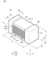
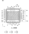
- FIG. 1 is an external perspective view showing a multilayer ceramic capacitor as an example of a multilayer ceramic capacitor according to an embodiment of the present invention
- 1 is a front view showing a multi-layer ceramic capacitor as an example of a multi-layer ceramic capacitor according to an embodiment of the present invention
- 1 is a plan view showing a multilayer ceramic capacitor as an example of a multilayer ceramic capacitor according to an embodiment of the present invention
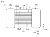
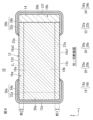
- FIG. 2 is a schematic cross-sectional view taken along line IV-IV in FIG.
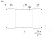
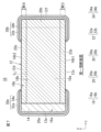
- FIG. 2 is a schematic cross-sectional view taken along line VV in FIG.
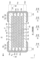
- FIG. 6 is a schematic cross-sectional view taken along line VI-VI in FIG. 4.
- FIG. 7 is a schematic cross-sectional view taken along line VII-VII in FIG. 4.
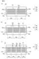
- FIG. 1A is a cross-sectional view taken along line II-II in FIG. 1 showing a structure in which a counter electrode portion of an internal electrode layer of a multilayer ceramic capacitor according to an embodiment of the present invention is divided into two
- FIG. 1B is a cross-sectional view taken along line II-II in FIG. 1 showing a structure in which a counter electrode portion of an internal electrode layer of a multilayer ceramic capacitor according to an embodiment of the present invention is divided into three
- FIG. 1C is a cross-sectional view taken along line II-II in FIG. 1 showing a structure in which a counter electrode portion of an internal electrode layer of a multilayer ceramic capacitor according to an embodiment of the present invention is divided into four.
- FIG. 1 is an external perspective view of a multilayer ceramic capacitor as an example of a multilayer ceramic capacitor according to an embodiment of the present invention.
- FIG. 2 is a front view of a multilayer ceramic capacitor as an example of a multilayer ceramic capacitor according to an embodiment of the present invention.
- FIG. 3 is a plan view of a multilayer ceramic capacitor as an example of a multilayer ceramic capacitor according to an embodiment of the present invention.
- FIG. 4 is a cross-sectional schematic diagram taken along line IV-IV in FIG. 1.
- FIG. 5 is a cross-sectional schematic diagram taken along line V-V in FIG. 1.
- FIG. 6 is a cross-sectional schematic diagram taken along line VI-VI in FIG. 4.
- FIG. 4 is a cross-sectional schematic diagram taken along line VI-VII in FIG. 1.
- the multilayer ceramic capacitor 10 has a laminate 12 and an external electrode 30.
- the laminate 12 is made up of a plurality of dielectric layers 14 and a plurality of internal electrode layers 16 stacked alternately, and is composed of an inner layer 15a that exhibits capacitance, and a first outer layer 15b1 and a second outer layer 15b2 that are arranged to sandwich the inner layer 15a from the upper and lower main surfaces.
- the laminate 12 has a plurality of dielectric layers 14 and a plurality of internal electrode layers 16 stacked together. Furthermore, the laminate 12 includes a first main surface 12a and a second main surface 12b that face the height direction x, which is the stacking direction of the plurality of dielectric layers 14, a first side surface 12c and a second side surface 12d that face the width direction y perpendicular to the height direction x, and a first end surface 12e and a second end surface 12f that face the length direction z perpendicular to the height direction x and the width direction y.
- the length direction z is also defined as an L direction that is a direction connecting the first end surface 12e and the second end surface 12f.
- the width direction y is also defined as a W direction that is a direction connecting the first side surface 12c and the second side surface 12d.
- the height direction x is also defined as a T direction that is a direction connecting the first main surface 12a and the second main surface 12b.
- the laminate 12 has a rectangular parallelepiped shape.
- the "rectangular parallelepiped shape” includes a rectangular parallelepiped with rounded corners and ridges. A corner is a portion where three adjacent faces of the laminate 12 intersect, and a ridge is a portion where two adjacent faces of the laminate 12 intersect.
- a “rectangular parallelepiped” member refers to any member that has a first main surface 12a and a second main surface 12b, a first side surface 12c and a second side surface 12d, and a first end surface 12e and a second end surface 12f.
- the first main surface 12a and the second main surface 12b, the first side surface 12c and the second side surface 12d, and the first end surface 12e and the second end surface 12f may have irregularities or the like formed in part or all of them.
- the laminate 12 has an inner layer portion 15a in which multiple internal electrode layers 16 face each other in the height direction x connecting the first main surface 12a and the second main surface 12b, a first outer layer portion 15b1 formed from multiple dielectric layers 14 located between the internal electrode layer 16 located closest to the first main surface 12a and the first main surface 12a, and a second outer layer portion 15b2 formed from multiple dielectric layers 14 located between the internal electrode layer 16 located closest to the second main surface 12b and the second main surface 12b.
- the first outer layer 15b1 is located on the first main surface 12a side of the laminate 12, and is an assembly of multiple dielectric layers 14 located between the first main surface 12a and the internal electrode layer 16 closest to the first main surface 12a.
- the second outer layer 15b2 is located on the second main surface 12b side of the laminate 12 and is an assembly of multiple dielectric layers 14 located between the second main surface 12b and the internal electrode layer 16 closest to the second main surface 12b.
- the area sandwiched between the first outer layer 15b1 and the second outer layer 15b2 is the inner layer 15a.
- the laminate 12 is located between the inner layer portion 15a and the first end face 12e, and between the inner layer portion 15a and the second end face 12f, and includes an end portion 22b (L gap) of the laminate 12 that includes an extraction electrode portion of either the first internal electrode layer 16a or the second internal electrode layer 16b, which will be described later.
- the number of dielectric layers 14 to be stacked is not particularly limited, but is preferably 50 to 1000, including the first outer layer 15b1 and the second outer layer 15b2.
- the thickness of the dielectric layers 14 is preferably, for example, about 0.5 ⁇ m to 10 ⁇ m.
- the dielectric layer 14 may be formed of, for example, a dielectric material.
- a dielectric ceramic composed of a main component such as BaTiO 3 , CaTiO 3 , SrTiO 3 , or CaZrO 3 may be used.
- a subcomponent may be added that is less in content than the main component, such as a Mn compound, an Fe compound, a Cr compound, a Co compound, or a Ni compound.
- Mg is used.
- the internal electrode layer 16 includes a first internal electrode layer 16a and a second internal electrode layer 16b.
- the first internal electrode layer 16a and the second internal electrode layer 16b are alternately stacked with the dielectric layer 14 interposed therebetween.
- the first internal electrode layer 16a is disposed on the surface of the dielectric layer 14.
- the first internal electrode layer 16a has a first opposing electrode portion 18a that faces the second internal electrode layer 16b, and a first lead electrode portion 20a that is located on one end side of the first internal electrode layer 16a and reaches from the first opposing electrode portion 18a to the first end face 12e of the laminate 12.
- the end of the first lead electrode portion 20a is led out to the first end face 12e and exposed.
- the end of the first lead electrode portion 20a is slightly recessed from the second end face 12f.
- the shape of the first opposing electrode portion 18a of the first internal electrode layer 16a is not particularly limited, but is preferably rectangular in plan view. However, the corners in plan view may be rounded or may be formed at an angle in plan view (tapered).
- the shape of the first extraction electrode portion 20a of the first internal electrode layer 16a is not particularly limited, but is preferably rectangular in plan view. However, the corners in plan view may be rounded or may be formed at an angle in plan view (tapered). It may also be tapered in plan view, with a slope in either direction.
- the second internal electrode layer 16b is disposed on a surface of a dielectric layer 14 different from the dielectric layer 14 on which the first internal electrode layer 16a is disposed. It has a second opposing electrode portion 18b that faces the first internal electrode layer 16a, and a second extraction electrode portion 20b that is located on one end side of the second internal electrode layer 16b and reaches from the second opposing electrode portion 18b to the second end face 12f of the laminate 12.
- the end of the second extraction electrode portion 20b is extended to the second end face 12f and exposed.
- the end of the second extraction electrode portion 20b is slightly recessed from the first end face 12e.
- the shape of the second opposing electrode portion 18b of the second internal electrode layer 16b is not particularly limited, but is preferably rectangular in plan view. However, the corners in plan view may be rounded or may be formed at an angle in plan view (tapered).
- the shape of the second extraction electrode portion 20b of the second internal electrode layer 16b is not particularly limited, but is preferably rectangular in plan view. However, the corners in plan view may be rounded or may be formed at an angle in plan view (tapered). It may also be tapered in plan view, with a slope in either direction.
- the first opposing electrode portion 18a of the first internal electrode layer 16a and the second opposing electrode portion 18b of the second internal electrode layer 16b face each other via the dielectric layer 14, forming a capacitance and exhibiting the characteristics of a capacitor.
- the number of stacked internal electrode layers 16 is not particularly limited, but is preferably 50 to 1000.
- the thickness of the internal electrode layers 16 is preferably about 0.2 ⁇ m to 2.0 ⁇ m.
- first internal electrode layer 16a and the second internal electrode layer 16b of the internal electrode layer 16 are exposed to the first side surface 12c and the second side surface 12d of the laminate 12.
- the first internal electrode layer 16a has a first edge 16a1, one of both edges along the width direction y, drawn out and exposed to the first side surface 12c.
- the first internal electrode layer 16a has a second edge 16a2, the other of both edges along the width direction y, drawn out and exposed to the second side surface 12d.
- the second internal electrode layer 16b has a third edge 16b1, one of both edges along the width direction y, drawn out and exposed to the first side surface 12c.
- the second internal electrode layer 16b has a fourth edge 16b2, the other of both edges along the width direction y, drawn out and exposed to the second side surface 12d.
- the first internal electrode layer 16a and the second internal electrode layer 16b are exposed on the first side surface 12c and the second side surface 12d in the laminate 12. This makes it possible to increase the effective area of the internal electrodes that contribute to capacitance expression. In addition, it is possible to omit the process of forming a dielectric layer on the side end side in the width direction y where the first side surface 12c and the second side surface 12d are located, thereby reducing manufacturing costs.
- the internal electrode layer 16 can be made of an appropriate conductive material, such as metals such as Ni, Cu, Ag, Pd, and Au, or alloys containing at least one of these metals, such as an Ag-Pd alloy. In particular, in this embodiment, it is preferable for the material to contain at least Ni.
- an insulating Ni-Mg-O phase is formed in the regions along the exposed portions of each of the first side 12c and second side 12d of the laminate 12 of the internal electrode layer 16.
- the first internal electrode layer 16a has a first region 23a along the first edge 16a1 on the first side surface 12c side, and a second region 25a along the second edge 16a2 on the second side surface 12d side, as shown in particular in Figures 5 and 6.
- the Ni-Mg-O phase is disposed in the first region 23a and the second region 25a.
- the second internal electrode layer 16b has a third region 23b along the third edge 16b1 on the first side surface 12c side, and a fourth region 25b along the fourth edge 16b2 on the second side surface 12d side.
- Ni-Mg-O phase is disposed in the third region 23b and the fourth region 25b.
- Ni-Mg-O phase is arranged in the first region 23a, second region 25a, third region 23b, and fourth region 25b.
- the oxide NiO produced during firing of the laminate 12 also has insulating properties, but arranging the Ni-Mg-O phase has the following advantages.
- the Ni-Mg-O phase is a solid solution, and once formed, it cannot be restored by an oxidation-reduction reaction.
- NiO returns to simple Ni in a reducing atmosphere.
- the Ni-Mg-O phase has higher chemical stability than NiO, and therefore can reliably ensure the insulation of the exposed portions of the internal electrode layer 16 on the first side surface 12c and the second side surface 12d of the laminate 12.
- the presence or absence of the Ni-Mg-O phase in the first region 23a, the second region 25a, the third region 23b, and the fourth region 25b can be analyzed using FE-WDX.
- it can also be identified from two images, a secondary electron image and a backscattered electron image.
- the dimension WE1 in the width direction y of the first region 23a and the dimension WE2 in the width direction y of the second region 25a i.e., the dimension in the width direction y, is 5 ⁇ m or more and 50 ⁇ m or less.
- the dimension WE3 in the width direction y of the third region 23b and the dimension WE4 in the width direction y of the fourth region 25b i.e., the dimension in the width direction y, is 5 ⁇ m or more and 50 ⁇ m or less.
- the coverage rate K3 of the second internal electrode layer 16b with respect to the dielectric layer 14 in the third region 23b and the fourth region 25b is preferably lower than the coverage rate K4 of the second internal electrode layer 16b with respect to the dielectric layer 14 in the central portion C2 in the width direction y of the laminate 12.
- the central portion C2 in the width direction y of the laminate 12 refers to the region sandwiched between the third region 23b and the fourth region 25b in the width direction y of the second internal electrode layer 16b.
- the coverage rate K1 is 40% or more and 70% or less
- the coverage rate K3 is 40% or more and 70% or less. If the coverage rates K1 and K3 are less than 40%, the volume expansion of the Ni-Mg-O phase causes microcracks in the laminate 12, and the failure rate in the moisture resistance test increases. On the other hand, if the coverage rates K1 and K3 are greater than 70%, the proportion of the Ni-Mg-O phase in each region decreases, reducing insulation, and increasing the failure rate for short circuits.
- the coverage rate of the internal electrode layer 16 on the dielectric layer 14 is generally measured as follows. That is, the internal electrode layer 16 and the dielectric layer 14 located in the center of the laminate 12 in the T direction are peeled off by electrochemical peeling or the like. Next, the center of the exposed internal electrode layer 16 (1/2 in the W direction and 1/2 in the L direction) is observed using a microscope at a magnification of about 100x. The image obtained is then analyzed to determine the proportion of the area of the exposed portion that is occupied by the internal electrode layer 16, which is the coverage rate.
- the laminate 12 shown in FIG. 1 may have a floating internal electrode layer 16c that is not drawn out to either the first end face 12e or the second end face 12f, in addition to the first internal electrode layer 16a and the second internal electrode layer 16b, and the floating internal electrode layer 16c may divide the opposing electrode portion 26c into multiple parts.
- the opposing electrode portion 26c may have a two-way structure as shown in FIG. 8(a), a three-way structure as shown in FIG. 8(b), a four-way structure as shown in FIG. 8(c), or a structure of more than four parts.
- the opposing electrode portion 26c by dividing the opposing electrode portion 26c into multiple parts, multiple capacitor components are formed between the opposing first internal electrode layer 16a, the second internal electrode layer 16b, and the floating internal electrode layer 16c, and these capacitor components are connected in series. Therefore, the voltage applied to each capacitor component is reduced, and the multilayer ceramic capacitor 10 can have a high withstand voltage.
- the floating internal electrode layer 16c can be made of an appropriate conductive material, such as a metal such as Ni, Cu, Ag, Pd, or Au, or an alloy containing at least one of these metals, such as an Ag-Pd alloy.
- external electrodes 30 are arranged on the first end face 12e and the second end face 12f of the laminate 12.
- the external electrode 30 includes a base electrode layer 32 containing a metal component and glass, and a plating layer 34 disposed on the surface of the base electrode layer 32.
- the external electrode 30 has a first external electrode 30a and a second external electrode 30b.
- the first external electrode 30a is connected to the first internal electrode layer 16a and is disposed on at least the surface of the first end face 12e.
- the first external electrode 30a also extends from the first end face 12e of the laminate 12 and is disposed on a part of the first main face 12a and a part of the second main face 12b, as well as a part of the first side face 12c and a part of the second side face 12d.
- the first external electrode 30a is electrically connected to the first lead-out electrode portion 20a of the first internal electrode layer 16a.
- the second external electrode 30b is connected to the second internal electrode layer 16b and is disposed on at least the surface of the second end face 12f.
- the second external electrode 30b also extends from the second end face 12f of the laminate 12 and is disposed on a part of the first main face 12a and a part of the second main face 12b, as well as a part of the first side face 12c and a part of the second side face 12d.
- the second external electrode 30b is electrically connected to the second extraction electrode portion 20b of the second internal electrode layer 16b.
- the first opposing electrode portion 18a of the first internal electrode layer 16a and the second opposing electrode portion 18b of the second internal electrode layer 16b face each other via the dielectric layer 14, forming a capacitance. Therefore, a capacitance is obtained between the first external electrode 30a to which the first internal electrode layer 16a is connected and the second external electrode 30b to which the second internal electrode layer 16b is connected, and the characteristics of a capacitor are expressed.
- the base electrode layer 32 has a first base electrode layer 32a and a second base electrode layer 32b.
- the first base electrode layer 32a is connected to the first internal electrode layer 16a and is disposed on the surface of the first end face 12e.
- the first base electrode layer 32a also extends from the first end face 12e and is disposed on a part of the first main face 12a and a part of the second main face 12b, as well as a part of the first side face 12c and a part of the second side face 12d.
- the first base electrode layer 32a is electrically connected to the first lead electrode portion 20a of the first internal electrode layer 16a.
- the second base electrode layer 32b is connected to the second internal electrode layer 16b and is disposed on the surface of the second end face 12f.
- the second base electrode layer 32b also extends from the second end face 12f and is disposed on a part of the first main face 12a and a part of the second main face 12b, as well as a part of the first side face 12c and a part of the second side face 12d.
- the second base electrode layer 32b is electrically connected to the second lead electrode portion 20b of the second internal electrode layer 16b.
- the base electrode layer 32 includes at least one selected from a baked layer, a conductive resin layer, a thin film layer, etc.
- the baking layer includes a metal component and glass.
- the metal component of the baking layer includes at least one selected from, for example, Cu, Ni, Ag, Pd, Ag-Pd alloy, Au, and the like.
- the baking layer is formed by applying a conductive paste containing glass and a metal to the laminate and baking it.
- the baking layer is formed by simultaneously baking the laminated chip having the internal electrode layer 16 and the dielectric layer 14 and the conductive paste applied to the laminated chip, but may be baked after baking the laminated chip having the internal electrode layer 16 and the dielectric layer 14.
- the baking layer may be a multi-layered layer.
- the thickness in the length direction z connecting the first end face 12e and the second end face 12f at the center of the height direction x of the first base electrode layer 32a located on the first end face 12e is preferably, for example, about 10 ⁇ m or more and 150 ⁇ m or less.
- the thickness in the length direction z connecting the first end face 12e and the second end face 12f at the center in the height direction x of the second base electrode layer 32b located on the second end face 12f is preferably, for example, about 10 ⁇ m or more and 150 ⁇ m or less.
- the thickness in the height direction x connecting the first principal surface 12a and the second principal surface 12b at the center of the length direction z connecting the first end surface 12e and the second end surface 12f of the first base electrode layer 32a located on a part of the first principal surface 12a and the second principal surface 12b is preferably, for example, about 10 ⁇ m or more and 100 ⁇ m or less.
- the thickness in the height direction x connecting the first principal surface 12a and the second principal surface 12b at the center of the length direction z connecting the first end surface 12e and the second end surface 12f of the second base electrode layer 32b located on a part of the first principal surface 12a and the second principal surface 12b is preferably, for example, about 10 ⁇ m or more and 100 ⁇ m or less.
- the thickness in the width direction y connecting the first side surface 12c and the second side surface 12d at the center of the length direction z connecting the first end surface 12e and the second end surface 12f of the first base electrode layer 32a located on a part of the first side surface 12c and the second side surface 12d is preferably, for example, about 10 ⁇ m or more and 100 ⁇ m or less.
- the thickness in the width direction y connecting the first side surface 12c and the second side surface 12d at the center of the length direction z connecting the first end surface 12e and the second end surface 12f of the second base electrode layer 32b located on a part of the first side surface 12c and the second side surface 12d is preferably, for example, about 10 ⁇ m or more and 100 ⁇ m or less.
- the conductive resin layer includes a first conductive resin layer and a second conductive resin layer.
- the first conductive resin layer is preferably arranged as a first base electrode layer 32a so as to further cover other layers such as a baked layer
- the second conductive resin layer is preferably arranged as a second base electrode layer 32b so as to further cover other layers such as a baked layer.
- the first conductive resin layer and the second conductive resin layer are preferably disposed as the first base electrode layer 32a and the second base electrode layer 32b on other layers such as baked layers located on the first end face 12e and the second end face 12f, and are also preferably disposed so as to extend onto other layers such as baked layers located on the first main face 12a and the second main face 12b, and the first side face 12c and the second side face 12d.
- the first conductive resin layer and the second conductive resin layer may be disposed only on other layers such as baked layers located on the first end face 12e and the second end face 12f.
- the thickness of the first conductive resin layer and the second conductive resin layer is preferably, for example, about 10 ⁇ m or more and 200 ⁇ m or less.
- the first conductive resin layer and the second conductive resin layer contain a thermosetting resin and a metal component.
- the first conductive resin layer and the second conductive resin layer contain a thermosetting resin, and therefore are more flexible than the base electrode layer 32, which is made of, for example, a plating film or a fired conductive paste. Therefore, even if the multilayer ceramic capacitor 10 is subjected to a physical shock or a shock caused by a thermal cycle, the conductive resin layer functions as a buffer layer and can prevent cracks in the multilayer ceramic capacitor 10.
- thermosetting resins that can be used include various known thermosetting resins such as epoxy resin, phenolic resin, urethane resin, silicone resin, and polyimide resin.
- epoxy resin is one of the most suitable resins due to its excellent heat resistance, moisture resistance, and adhesion.
- the first conductive resin layer and the second conductive resin layer preferably contain a curing agent in addition to the thermosetting resin.
- a curing agent in addition to the thermosetting resin.
- various known compounds such as phenol-based, amine-based, acid anhydride-based, and imidazole-based compounds can be used as the curing agent for the epoxy resin.
- the metal contained in the first conductive resin layer and the second conductive resin layer may be Ag, Cu, or an alloy thereof.
- Metal powder with an Ag-coated surface may also be used. When using metal powder with an Ag-coated surface, it is preferable to use Cu or Ni as the metal powder.
- the metal contained in the first conductive resin layer and the second conductive resin layer is preferably contained in an amount of 35 vol% or more and 75 vol% or less relative to the total volume of the conductive resin.
- the shape of the metal contained in the first conductive resin layer and the second conductive resin layer is not particularly limited.
- the conductive filler may be spherical, flat, etc.
- the average particle size of the metal contained in the first conductive resin layer and the second conductive resin layer is not particularly limited.
- the average particle size of the conductive filler may be, for example, about 0.3 ⁇ m or more and 10 ⁇ m or less.
- the metals contained in the first conductive resin layer and the second conductive resin layer are mainly responsible for the electrical conductivity of the conductive resin layers. Specifically, electrical paths are formed inside the conductive resin layers as the conductive fillers come into contact with each other.
- the metal contained in the first conductive resin layer and the second conductive resin layer may be spherical or flat, but it is preferable to use a mixture of spherical metal powder and flat metal powder.
- the conductive resin layer may be formed directly on the laminate without forming a baked layer.
- the thin film layer is formed by a thin film formation method such as sputtering or vapor deposition, and is a layer of 10 ⁇ m or less in thickness in which metal particles are deposited.
- first plating layer 34a and the second plating layer 34b which are the plating layers 34 disposed on the base electrode layer 32, will be described with reference to Figures 2 and 3.
- the first plating layer 34a and the second plating layer 34b include, for example, at least one selected from Cu, Ni, Sn, Ag, Pd, Ag-Pd alloy, Au, etc.
- the first plating layer 34a is disposed so as to completely cover the first base electrode layer 32a.
- the second plating layer 34b is disposed so as to completely cover the second base electrode layer 32b.
- the first plating layer 34a and the second plating layer 34b may be formed of a plurality of layers.
- the plating layer 34 preferably has a two-layer structure including a lower plating layer (Ni plating layer) formed on the base electrode layer 32 by Ni plating, and an upper plating layer (Sn plating layer) formed on the lower plating layer by Sn plating. That is, in this case, the first plating layer 34a has a first lower plating layer and a first upper plating layer located on the surface of the first lower plating layer.
- the second plating layer 34b has a second lower plating layer and a second upper plating layer located on the surface of the second lower plating layer.
- the lower plating layer made of Ni plating is used to prevent the base electrode layer 32 from being eroded by solder when mounting the multilayer ceramic capacitor 10, and the upper plating layer made of Sn plating is used to improve the wettability of the solder when mounting the multilayer ceramic capacitor 10, making it easier to mount.
- each of the lower plating layer and the upper plating layer is preferably 1.0 ⁇ m or more and 15.0 ⁇ m or less.
- the dimension in the length direction z of the multilayer ceramic capacitor 10, including the laminate 12, the first external electrode 30a, and the second external electrode 30b, is defined as dimension L
- the dimension in the height direction x of the multilayer ceramic capacitor 10, including the laminate 12, the first external electrode 30a, and the second external electrode 30b is defined as dimension T
- the dimension in the width direction y of the multilayer ceramic capacitor 10, including the laminate 12, the first external electrode 30a, and the second external electrode 30b is defined as dimension W.
- the dimensions of the multilayer ceramic capacitor 10 are: L dimension in the length direction z is 0.2 mm to 10.0 mm, W dimension in the width direction y is 0.1 mm to 10.0 mm, and T dimension in the height direction x is 0.1 mm to 5.0 mm.
- the dimensions of the multilayer ceramic capacitor 10 can be measured using a microscope.
- the first internal electrode layer 16a and the second internal electrode layer 16b of the internal electrode layer 16 are exposed on the first side surface 12c and the second side surface 12d of the laminate 12, respectively.
- This allows the effective area of the internal electrodes that contribute to the generation of capacitance to be increased in the multilayer ceramic capacitor 10.
- the process of forming a dielectric layer on the side end side in the width direction y where the first side surface 12c and the second side surface 12d are located can be omitted, thereby reducing the manufacturing cost of the multilayer ceramic capacitor 10.
- an insulating Ni-Mg-O phase is preferably formed in the first region 23a along the first edge 16a1 on the first side surface 12c side of the laminate 12, the second region 25a along the second edge 16a2 on the second side surface 12d side of the laminate 12, the third region 23b along the third edge 16b1 on the first side surface 12c side of the laminate 12, and the fourth region 25b along the fourth edge 16b2 on the second side surface 12d side of the laminate 12.
- the dimension WE1 in the width direction y of the first region 23a and the dimension WE2 in the width direction y of the second region 25a are preferably 5 ⁇ m or more and 50 ⁇ m or less.
- the dimension WE3 in the width direction y of the third region 23b and the dimension WE4 in the width direction y of the fourth region 25b are preferably 5 ⁇ m or more and 50 ⁇ m or less.
- the coverage K1 of the first internal electrode layer 16a with respect to the dielectric layer 14 in the first region 23a and the second region 25a is preferably lower than the coverage K2 of the first internal electrode layer 16a with respect to the dielectric layer 14 in the central portion C1 in the width direction y of the laminate 12.
- the coverage K3 of the second internal electrode layer 16b with respect to the dielectric layer 14 in the third region 23b and the fourth region 25b is preferably lower than the coverage K4 of the second internal electrode layer 16b with respect to the dielectric layer 14 in the central portion C2 in the width direction y of the laminate 12. This effectively reduces the dimension of the W gap, and the effect of ensuring insulation in each region can be further improved.
- the coverage rate K1 is 40% or more and 70% or less
- the coverage rate K3 is 40% or more and 70% or less.
- the dielectric sheet and the conductive paste for the internal electrode layers contain a binder (e.g., a known organic binder) and a solvent (e.g., a known organic binder).
- a binder e.g., a known organic binder
- a solvent e.g., a known organic binder
- a conductive paste for the internal electrode layers is printed in stripes on the dielectric sheet in a predetermined pattern, for example by screen printing or gravure printing, to prepare a dielectric sheet on which a first internal electrode pattern corresponding to the first internal electrode layer is formed, and a dielectric sheet on which a second internal electrode pattern corresponding to the second internal electrode layer is formed.
- a dielectric sheet for an outer layer on which no internal electrode pattern is printed is also prepared.
- a predetermined number of dielectric sheets for the outer layer on which no internal electrode pattern is formed are stacked to form the outer layer portion, and a dielectric sheet on which a first internal electrode pattern is formed and a dielectric sheet on which a second internal electrode pattern is formed are stacked on top of the outer layer portion, shifted in the width direction (short direction) of the striped pattern, to form the inner layer portion.
- a predetermined number of dielectric sheets on which no internal electrode pattern is printed are then stacked on top of the internal electrode pattern corresponding to the internal electrode layer located on the outermost surface of the inner layer to form the outer layer, thereby producing a laminated sheet.
- the laminated sheets are pressed in the stacking direction using a means such as a hydrostatic press to produce a laminated block.
- the laminated block is cut to a predetermined size to produce laminated chips.
- the corners and edges of the laminated chips may be rounded by barrel polishing or the like.
- the laminated chip is fired to produce the laminate 12.
- the firing temperature depends on the ceramic and the material of the internal electrode layer 16, but is preferably 900°C or higher and 1400°C or lower. In particular, by adjusting the oxygen concentration in the range of 900°C or higher and 1100°C or lower, a Ni-Mg-O phase can be formed in the regions along both edges of the internal electrode layer 16 in the width direction y dimension of the fired laminate 12.
- a conductive paste is applied to the first end face and the second end face, which are both end faces of the laminate 12, for example, by a method such as dipping or screen printing, and then a baking process is performed to form a first base electrode layer and a second base electrode layer.
- the temperature of the baking process at this time is preferably 700°C or higher and 900°C or lower.
- the conductive resin layer can be formed by the following method.
- the conductive resin layer may be formed on the surface of the baked layer, or the conductive resin layer may be formed directly on the laminate without forming a baked layer.
- the conductive resin layer is formed by applying a conductive resin paste containing a thermosetting resin and a metal component onto the baking layer or the laminate 12, and then performing a heat treatment at a temperature of 250°C to 550°C to thermally cure the resin and form a conductive resin layer.
- the atmosphere during the heat treatment is preferably an N2 atmosphere.
- the surface of the base electrode layer is plated to form a plating layer.
- two plating layers are formed on the surfaces of the first and second base electrode layers.
- a Ni plating layer is formed on the first and second base electrode layers, and a Sn plating layer is formed on the Ni plating layer.
- the Ni plating layer and the Sn plating layer are formed sequentially, for example, by barrel plating.
- the multilayer ceramic capacitor 10 according to the embodiment shown in Figure 1 is manufactured.
- Cap Measurement method of capacitance (Cap)
- the capacitance (Cap) was measured using a meter (4278A manufactured by Agilent Technologies) at 120 Hz and 0.5 Vrms to measure the capacitance (C).
- the criteria for the capacitance (Cap) were as follows: 18.7 to 25.3 (good); 17.6 to 18.7 (good); and 17.6 or less and 25.3 or more (bad).
- Table 1 shows the evaluations of the insulation properties and capacitance of the dielectric layers of the laminates according to Examples 1 to 7 and the Comparative Example, as well as an overall evaluation.
- each of the samples in Examples 1 to 7 has a first region to a fourth region in which the Ni-Mg-O phase is arranged in the internal electrode layer, so that the samples obtained have good insulation properties.
- the length in the width direction y of the first region to the fourth region in which the Ni-Mg-O phase is arranged in the internal electrode layer is 5 ⁇ m or more and 50 ⁇ m or less, so the insulation measurement results were better, with a value of 7.5 or more.
- the internal electrode layer did not have the first region to the fourth region in which the Ni-Mg-O phase was arranged, and therefore insulation was not obtained.
- the effective area of the internal electrode that contributes to capacitance expression can be expanded.
- Multilayer ceramic capacitor 12 Laminate 12a First main surface 12b Second main surface 12c First side surface 12d Second side surface 12e First end surface 12f Second end surface 14 Dielectric layer 15a Inner layer portion 15b1 First outer layer portion 15b2 Second outer layer portion 16 Internal electrode layer 16a First internal electrode layer 16a1 First edge 16a2 Second edge 16b Second internal electrode layer 16b1 Third edge 16b2 Fourth edge 16c Floating internal electrode layer 18a First opposing electrode portion 18b Second opposing electrode portion 20a First lead electrode portion 20b Second lead electrode portion 22b End portion 23a First region 23b Third region 25a Second region 25b Fourth region 26c Counter electrode portion 30 External electrode 30a First external electrode 30b Second external electrode 32 Base electrode layer 32a First base electrode layer 32b Second base electrode layer 34 Plating layer 34a First plating layer 34b Second plating layer x Height direction (stacking direction) y Width direction z Length direction
Landscapes
- Engineering & Computer Science (AREA)
- Power Engineering (AREA)
- Manufacturing & Machinery (AREA)
- Microelectronics & Electronic Packaging (AREA)
- Chemical & Material Sciences (AREA)
- Ceramic Engineering (AREA)
- Inorganic Chemistry (AREA)
- Materials Engineering (AREA)
- Fixed Capacitors And Capacitor Manufacturing Machines (AREA)
- Ceramic Capacitors (AREA)
Abstract
Description
この発明の実施の形態にかかる積層セラミックコンデンサの一例である積層セラミックコンデンサ10について説明する。図1は、この発明の実施の形態にかかる積層セラミックコンデンサの一例である積層セラミックコンデンサを示す外観斜視図である。図2は、この発明の実施の形態にかかる積層セラミックコンデンサの一例である積層セラミックコンデンサを示す正面図である。図3は、この発明の実施の形態にかかる積層セラミックコンデンサの一例である積層セラミックコンデンサを示す平面図である。図4は、図1にかかる線IV-IVにおける断面模式図である。図5は、図1にかかる線V-Vにおける断面模式図である。図6は、図4にかかる線VI-VIにおける断面模式図である。図4は、図1にかかる線VI-VIIにおける断面模式図である。
積層体12は、積層された複数の誘電体層14と複数の内部電極層16とを有する。さらに、積層体12は、複数の誘電体層14の積層方向である高さ方向xに相対する第1の主面12aおよび第2の主面12bと、高さ方向xに直交する幅方向yに相対する第1の側面12cおよび第2の側面12dと、高さ方向xおよび幅方向yに直交する長さ方向zに相対する第1の端面12eおよび第2の端面12fとを含む。なお、長さ方向zは、第1の端面12eおよび第2の端面12fを結ぶ方向であるL方向としても定義される。幅方向yは、第1の側面12cおよび第2の側面12dを結ぶ方向であるW方向としても定義される。高さ方向xは、第1の主面12aおよび第2の主面12bを結ぶ方向であるT方向としても定義される。
内部電極層16は、図4および図5に示されるように、第1の内部電極層16aと第2の内部電極層16bとを有している。第1の内部電極層16aと第2の内部電極層16bは、誘電体層14を介して交互に積層される。
焼付け層は、金属成分とガラスとを含む。焼付け層の金属成分としては、たとえば、Cu、Ni、Ag、Pd、Ag-Pd合金、Au等から選ばれる少なくとも1つを含む。焼付け層は、ガラスおよび金属を含む導電性ペーストを積層体に塗布して焼付けたものである。焼付け層は、内部電極層16および誘電体層14を有する積層チップと積層チップに塗布した導電性ペーストとを同時焼成して形成するが、内部電極層16および誘電体層14を有する積層チップを焼成した後に焼き付けてもよい。焼付け層は、複数層であってもよい。
導電性樹脂層は、第1の導電性樹脂層と第2の導電性樹脂層とを有する。
下地電極層32を薄膜層で形成する場合、薄膜層は、スパッタ法または蒸着法等の薄膜形成法により形成され、金属粒子が堆積された10μm以下の層である。
第2のめっき層34bは、第2の下地電極層32bを完全に覆うように配置されている。
すなわち、この場合、第1のめっき層34aは、第1の下層めっき層と、第1の下層めっき層の表面に位置する第1の上層めっき層とを有する。
また、第2のめっき層34bは、第2の下層めっき層と、第2の下層めっき層の表面に位置する第2の上層めっき層とを有する。
積層セラミックコンデンサ10の寸法は、長さ方向zのL寸法が0.2mm以上10.0mm以下、幅方向yのW寸法が0.1mm以上10.0mm以下、高さ方向xのT寸法が0.1mm以上5.0mm以下である。また、積層セラミックコンデンサ10の寸法は、マイクロスコープにより測定することができる。
次に、積層セラミックコンデンサの製造方法について説明する。
次に、上述した本発明にかかる積層セラミックコンデンサの効果を確認するために、実験の試料として上述した製造方法にしたがって、試料である積層セラミックコンデンサを作製し、第1の領域ないし第4の領域の幅方向yの変化および有無にともなう絶縁性と静電容量の変化を確認する実験を行った。
まず、上述した積層セラミックコンデンサの製造方法にしたがって、以下のような仕様の実施例1ないし実施例7にかかる積層セラミックコンデンサの試料を作製した。なお、比較例にかかる積層セラミックコンデンサは、製造方法の工程(7)の900℃以上1100℃以下の範囲で酸素濃度を実験例よりも低い状態にして焼成を行った。
・積層セラミックコンデンサの寸法(設計値):L×W×T=1.17mm×0.68mm×0.68mm
・誘電体層の主成分のセラミック材料:BaTiO3
・容量:22μF
・内部電極層の材料:Ni
・外部電極の構造:導電性金属(Cu)とガラス成分
・めっき層
Niめっき層とSnめっき層との2層形成
Niめっき層厚み:約3μm
Snめっき層厚み:約5μm
積層コンデンサの絶縁性は、定格電圧6.3V-1minの測定条件で、デジタル超高抵抗/微少電流計(ADCMT社製 5451)にて測定した。絶縁性(IR)に対する判定基準は、Log(IR)として6.8以上(150Ω・F)なので、ばらつきを考慮し、6.8以下を×、6.9以上7.4以下を△、7.5以上を〇とした。
静電容量(Cap)の測定は、メーター(Agilent Technologies社製 4278A)を用いて、120Hz、0.5Vrmsの条件で得られる静電容量(C)を測定した。静電容量(Cap)の判定基準は、18.7以上25.3以下を〇とし、17.6以上18.7以下を△とし、17.6以下および25.3以上を×とした。
表1に、実施例1ないし実施例7、ならびに比較例による積層体の誘電体層の絶縁性および静電容量の判定並びに総合判定を示す。

12 積層体
12a 第1の主面
12b 第2の主面
12c 第1の側面
12d 第2の側面
12e 第1の端面
12f 第2の端面
14 誘電体層
15a 内層部
15b1 第1の外層部
15b2 第2の外層部
16 内部電極層
16a 第1の内部電極層
16a1 第1の縁
16a2 第2の縁
16b 第2の内部電極層
16b1 第3の縁
16b2 第4の縁
16c 浮き内部電極層
18a 第1の対向電極部
18b 第2の対向電極部
20a 第1の引出電極部
20b 第2の引出電極部
22b 端部
23a 第1の領域
23b 第3の領域
25a 第2の領域
25b 第4の領域
26c 対向電極部
30 外部電極
30a 第1の外部電極
30b 第2の外部電極
32 下地電極層
32a 第1の下地電極層
32b 第2の下地電極層
34 めっき層
34a 第1のめっき層
34b 第2のめっき層
x 高さ方向(積層方向)
y 幅方向
z 長さ方向
Claims (3)
- 積層された複数の誘電体層を含み、前記複数の誘電体層の積層方向に相対する第1の主面および第2の主面と、前記積層方向に直交する幅方向に相対する第1の側面および第2の側面と、前記積層方向および前記幅方向に直交する長さ方向に相対する第1の端面および第2の端面と、を有する積層体と、
前記複数の誘電体層上に配置され、前記第1の端面に露出された第1の内部電極層と、
前記複数の誘電体層上に配置され、前記第2の端面に露出された第2の内部電極層と、
前記第1の端面上に配置された下地電極層と、前記下地電極層に上に配置されためっき層と、を有する第1の外部電極と、
前記第2の端面上に配置された下地電極層と、前記下地電極層に上に配置されためっき層と、を有する第2の外部電極と、
を備える積層セラミックコンデンサにおいて、
前記第1の内部電極層は、前記第1の側面および第2の側面に露出し、
前記第2の内部電極層は、前記第1の側面および第2の側面に露出しており、
前記第1の内部電極層は、前記積層体の前記第1の側面側の縁に沿った第1の領域と、前記積層体の前記第2の側面側の縁に沿った第2の領域とを有し、
前記第1の領域および前記第2の領域には、Ni-Mg-O相が形成されており、
前記第2の内部電極層は、前記積層体の前記第1の側面側の縁に沿った第3の領域と、前記積層体の前記第2の側面側の縁に沿った第4の領域とを有し、
前記第3の領域および前記第4の領域には、Ni-Mg-O相が形成されている、積層セラミックコンデンサ。 - 前記第1の領域および前記第2の領域の各々の幅方向の寸法は、5μm以上50μm以下であり、
前記第3の領域および前記第4の領域の各々の幅方向の寸法は、5μm以上50μm以下である、請求項1に記載の積層セラミックコンデンサ。 - 前記誘電体層は、少なくともMgを含む、請求項1または請求項2に記載の積層セラミックコンデンサ。
Priority Applications (6)
| Application Number | Priority Date | Filing Date | Title |
|---|---|---|---|
| CN202380068015.9A CN119968689A (zh) | 2023-08-18 | 2023-08-18 | 层叠陶瓷电容器 |
| JP2025541173A JPWO2025041211A1 (ja) | 2023-08-18 | 2023-08-18 | |
| PCT/JP2023/029904 WO2025041211A1 (ja) | 2023-08-18 | 2023-08-18 | 積層セラミックコンデンサ |
| KR1020257035557A KR20250168469A (ko) | 2023-08-18 | 2023-08-18 | 적층 세라믹 콘덴서 |
| TW113122642A TWI924034B (zh) | 2023-08-18 | 2024-06-19 | 積層陶瓷電容器 |
| US18/788,202 US20250062073A1 (en) | 2023-08-18 | 2024-07-30 | Multilayer ceramic capacitor |
Applications Claiming Priority (1)
| Application Number | Priority Date | Filing Date | Title |
|---|---|---|---|
| PCT/JP2023/029904 WO2025041211A1 (ja) | 2023-08-18 | 2023-08-18 | 積層セラミックコンデンサ |
Related Child Applications (1)
| Application Number | Title | Priority Date | Filing Date |
|---|---|---|---|
| US18/788,202 Continuation US20250062073A1 (en) | 2023-08-18 | 2024-07-30 | Multilayer ceramic capacitor |
Publications (1)
| Publication Number | Publication Date |
|---|---|
| WO2025041211A1 true WO2025041211A1 (ja) | 2025-02-27 |
Family
ID=94608578
Family Applications (1)
| Application Number | Title | Priority Date | Filing Date |
|---|---|---|---|
| PCT/JP2023/029904 Pending WO2025041211A1 (ja) | 2023-08-18 | 2023-08-18 | 積層セラミックコンデンサ |
Country Status (5)
| Country | Link |
|---|---|
| US (1) | US20250062073A1 (ja) |
| JP (1) | JPWO2025041211A1 (ja) |
| KR (1) | KR20250168469A (ja) |
| CN (1) | CN119968689A (ja) |
| WO (1) | WO2025041211A1 (ja) |
Citations (5)
| Publication number | Priority date | Publication date | Assignee | Title |
|---|---|---|---|---|
| JPS61248413A (ja) | 1985-04-25 | 1986-11-05 | 株式会社村田製作所 | 積層セラミツクコンデンサの製造方法 |
| JPH11111553A (ja) * | 1997-09-30 | 1999-04-23 | Kyocera Corp | 積層セラミックコンデンサ |
| JP2009016796A (ja) * | 2007-06-08 | 2009-01-22 | Murata Mfg Co Ltd | 積層セラミック電子部品 |
| JP2009224503A (ja) * | 2008-03-14 | 2009-10-01 | Tdk Corp | 積層コンデンサ |
| JP2012227197A (ja) * | 2011-04-15 | 2012-11-15 | Taiyo Yuden Co Ltd | 積層セラミックコンデンサ |
Family Cites Families (5)
| Publication number | Priority date | Publication date | Assignee | Title |
|---|---|---|---|---|
| CN102640239B (zh) * | 2009-12-11 | 2015-06-17 | 株式会社村田制作所 | 层叠型陶瓷电子部件 |
| JP5146852B2 (ja) * | 2010-03-05 | 2013-02-20 | 株式会社村田製作所 | 積層セラミックコンデンサ |
| KR101412950B1 (ko) * | 2012-11-07 | 2014-06-26 | 삼성전기주식회사 | 적층 세라믹 커패시터 |
| JP2017204560A (ja) * | 2016-05-11 | 2017-11-16 | 株式会社村田製作所 | 積層セラミックコンデンサ及びその製造方法 |
| JP7089404B2 (ja) * | 2018-05-22 | 2022-06-22 | 太陽誘電株式会社 | セラミック電子部品およびその製造方法 |
-
2023
- 2023-08-18 CN CN202380068015.9A patent/CN119968689A/zh active Pending
- 2023-08-18 JP JP2025541173A patent/JPWO2025041211A1/ja active Pending
- 2023-08-18 KR KR1020257035557A patent/KR20250168469A/ko active Pending
- 2023-08-18 WO PCT/JP2023/029904 patent/WO2025041211A1/ja active Pending
-
2024
- 2024-07-30 US US18/788,202 patent/US20250062073A1/en active Pending
Patent Citations (5)
| Publication number | Priority date | Publication date | Assignee | Title |
|---|---|---|---|---|
| JPS61248413A (ja) | 1985-04-25 | 1986-11-05 | 株式会社村田製作所 | 積層セラミツクコンデンサの製造方法 |
| JPH11111553A (ja) * | 1997-09-30 | 1999-04-23 | Kyocera Corp | 積層セラミックコンデンサ |
| JP2009016796A (ja) * | 2007-06-08 | 2009-01-22 | Murata Mfg Co Ltd | 積層セラミック電子部品 |
| JP2009224503A (ja) * | 2008-03-14 | 2009-10-01 | Tdk Corp | 積層コンデンサ |
| JP2012227197A (ja) * | 2011-04-15 | 2012-11-15 | Taiyo Yuden Co Ltd | 積層セラミックコンデンサ |
Also Published As
| Publication number | Publication date |
|---|---|
| CN119968689A (zh) | 2025-05-09 |
| JPWO2025041211A1 (ja) | 2025-02-27 |
| TW202509961A (zh) | 2025-03-01 |
| KR20250168469A (ko) | 2025-12-02 |
| US20250062073A1 (en) | 2025-02-20 |
Similar Documents
| Publication | Publication Date | Title |
|---|---|---|
| JP7655713B2 (ja) | 積層セラミックコンデンサ | |
| US11476046B2 (en) | Multilayer ceramic capacitor | |
| KR102946082B1 (ko) | 적층형 커패시터 | |
| KR20190011219A (ko) | 적층 세라믹 콘덴서 | |
| US12198863B2 (en) | Multilayer ceramic electronic component having specified thickness ratio for different portions of external electrode | |
| US20200343047A1 (en) | Multilayer ceramic capacitor | |
| KR20190058239A (ko) | 적층 세라믹 커패시터 및 그 제조방법 | |
| KR102694713B1 (ko) | 적층형 전자 부품 | |
| JP2023043725A (ja) | 積層セラミックコンデンサ | |
| JP7704374B2 (ja) | 積層型電子部品 | |
| JP7758283B2 (ja) | 積層型電子部品 | |
| WO2025041211A1 (ja) | 積層セラミックコンデンサ | |
| KR102938186B1 (ko) | 적층형 커패시터 | |
| JP2023118067A (ja) | 積層型電子部品 | |
| JP2021168337A (ja) | 積層セラミックコンデンサ | |
| KR20220048221A (ko) | 적층형 커패시터 | |
| US20260011493A1 (en) | Multilayer ceramic capacitor | |
| JP4470463B2 (ja) | セラミック電子部品の製造方法 | |
| US20250125097A1 (en) | Multilayer electronic component | |
| US20230215640A1 (en) | Multilayer electronic component | |
| KR102449364B1 (ko) | 적층 세라믹 전자부품 | |
| WO2025126293A1 (ja) | 積層セラミックコンデンサ | |
| WO2024257450A1 (ja) | 積層セラミック部品 | |
| WO2025004487A1 (ja) | 積層セラミックコンデンサ | |
| WO2024018720A1 (ja) | 積層セラミックコンデンサ及び積層セラミックコンデンサの製造方法 |
Legal Events
| Date | Code | Title | Description |
|---|---|---|---|
| WWE | Wipo information: entry into national phase |
Ref document number: 202380068015.9 Country of ref document: CN |
|
| 121 | Ep: the epo has been informed by wipo that ep was designated in this application |
Ref document number: 23920281 Country of ref document: EP Kind code of ref document: A1 |
|
| WWP | Wipo information: published in national office |
Ref document number: 202380068015.9 Country of ref document: CN |
|
| ENP | Entry into the national phase |
Ref document number: 2025541173 Country of ref document: JP Kind code of ref document: A |
|
| WWE | Wipo information: entry into national phase |
Ref document number: 2025541173 Country of ref document: JP |
|
| ENP | Entry into the national phase |
Ref document number: 1020257035557 Country of ref document: KR Free format text: ST27 STATUS EVENT CODE: A-0-1-A10-A15-NAP-PA0105 (AS PROVIDED BY THE NATIONAL OFFICE) |
|
| WWE | Wipo information: entry into national phase |
Ref document number: KR1020257035557 Country of ref document: KR Ref document number: 1020257035557 Country of ref document: KR |
|
| WWP | Wipo information: published in national office |
Ref document number: 1020257035557 Country of ref document: KR |
|
| NENP | Non-entry into the national phase |
Ref country code: DE |