WO2025028421A1 - 反強磁性体材料,磁性体および絶縁体の二層膜,トンネル磁気抵抗素子,及び磁気メモリ - Google Patents
反強磁性体材料,磁性体および絶縁体の二層膜,トンネル磁気抵抗素子,及び磁気メモリ Download PDFInfo
- Publication number
- WO2025028421A1 WO2025028421A1 PCT/JP2024/026734 JP2024026734W WO2025028421A1 WO 2025028421 A1 WO2025028421 A1 WO 2025028421A1 JP 2024026734 W JP2024026734 W JP 2024026734W WO 2025028421 A1 WO2025028421 A1 WO 2025028421A1
- Authority
- WO
- WIPO (PCT)
- Prior art keywords
- layer
- antiferromagnetic
- insulator
- magnetic
- antiferromagnetic layer
- Prior art date
- Legal status (The legal status is an assumption and is not a legal conclusion. Google has not performed a legal analysis and makes no representation as to the accuracy of the status listed.)
- Pending
Links
Images




Classifications
-
- H—ELECTRICITY
- H10—SEMICONDUCTOR DEVICES; ELECTRIC SOLID-STATE DEVICES NOT OTHERWISE PROVIDED FOR
- H10B—ELECTRONIC MEMORY DEVICES
- H10B61/00—Magnetic memory devices, e.g. magnetoresistive RAM [MRAM] devices
-
- H—ELECTRICITY
- H10—SEMICONDUCTOR DEVICES; ELECTRIC SOLID-STATE DEVICES NOT OTHERWISE PROVIDED FOR
- H10N—ELECTRIC SOLID-STATE DEVICES NOT OTHERWISE PROVIDED FOR
- H10N50/00—Galvanomagnetic devices
- H10N50/10—Magnetoresistive devices
-
- H—ELECTRICITY
- H10—SEMICONDUCTOR DEVICES; ELECTRIC SOLID-STATE DEVICES NOT OTHERWISE PROVIDED FOR
- H10N—ELECTRIC SOLID-STATE DEVICES NOT OTHERWISE PROVIDED FOR
- H10N50/00—Galvanomagnetic devices
- H10N50/20—Spin-polarised current-controlled devices
-
- H—ELECTRICITY
- H10—SEMICONDUCTOR DEVICES; ELECTRIC SOLID-STATE DEVICES NOT OTHERWISE PROVIDED FOR
- H10N—ELECTRIC SOLID-STATE DEVICES NOT OTHERWISE PROVIDED FOR
- H10N52/00—Hall-effect devices
Definitions
- the present disclosure relates to an antiferromagnetic material, a two layer film of a magnetic body and an insulator, a tunnel magnetoresistive element, and a magnetic memory.
- a tunnel magnetoresistance element can be obtained by using an antiferromagnetic layer such as Mn 3 Sn as a ferromagnetic layer and sandwiching an insulating layer such as MgO between two antiferromagnetic layers.
- the object of the present invention is to obtain a tunnel magnetoresistance element and magnetic memory that have high heat resistance.
- the double-layered film of magnetic material and insulator has a layer of the above-mentioned ferromagnetic material and a layer of insulator laminated on the layer of ferromagnetic material.
- the tunneling magnetoresistance element has a second antiferromagnetic film layer stacked on the bilayer insulator.
- the magnetic memory includes a plurality of the tunneling magnetoresistance elements described above.
- the present invention makes it possible to obtain a tunnel magnetoresistance element and magnetic memory with high heat resistance.
- FIG. 1 is a cross-sectional view showing one embodiment of a two-layer film of a magnetic material and an insulator.
- 1 is a cross-sectional view showing an embodiment of a tunneling magnetoresistive element.
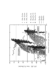
- the graph plots the average absolute value of the magnetic moment at each site on the horizontal axis and the difference ( ⁇ T N ) in Neel temperature (calculated value) compared to Mn 3 Sn on the vertical axis, with an upper limit of element substitution of 10%.
- 5A to 5C are cross-sectional views illustrating the operation of a tunnel magnetoresistive element.
- FIG. 2 is a circuit diagram of one embodiment of a magnetic memory.
- ranges When amounts, concentrations, or other values or parameters are given herein as ranges, and/or the description includes a list of upper and lower values, this is understood to specifically disclose all integers and fractions within the given range, as well as all ranges formed from any pair of any upper and lower values, whether or not a narrower range is separately disclosed.
- range of numerical values When a range of numerical values is given herein, unless otherwise stated, the range is intended to include all integers and fractions within the range, as well as its endpoints.
- the range of 1 to 10 fully describes and includes the independent subrange 3.4 to 7.2, as well as the listing of the values 1, 4, 6, and 10.
- Antiferromagnetic materials, bilayers of magnetic and insulating materials, and tunnel magnetoresistance elements 1 is a cross-sectional view showing one embodiment of a double-layered film of a magnetic material and an insulator. An insulator layer 12 is laminated on an antiferromagnetic layer 11.
- FIG. 2 is a cross-sectional view showing one embodiment of a tunnel magnetoresistance element.
- An insulating layer 12 is laminated on an antiferromagnetic layer 11, and a second antiferromagnetic layer 13 is further laminated on the insulating layer 12.
- A is more preferably at least one of Ga and Sn
- B is more preferably at least one of Mg, Al, Si, Mn, Cu, Zn, Ag, Cd, In, Sb, Au, and Tl.
- x is preferably 0 ⁇ x ⁇ 0.5, and more preferably 0.15 ⁇ x ⁇ 0.25.
- p is preferably 0 ⁇ p ⁇ 0.5, and more preferably 0.15 ⁇ p ⁇ 0.25.
- q is preferably 0.2 ⁇ q ⁇ 0.8, and more preferably 0.4 ⁇ q ⁇ 0.6.
- r is preferably r ⁇ 0.5.
- the materials of the antiferromagnetic layer 11 and the second antiferromagnetic layer 13 may be the same or different. These crystals have cluster magnetic octupole polarized spins, and the net spin polarization defined by the magnetic octupole can be rotated by applying a magnetic field or passing an electric current.
- the thickness of the antiferromagnetic layer 11 and the second antiferromagnetic layer 13 are each independently, for example, 0.5 nm to 40 nm, preferably 0.5 nm to 30 nm, and more preferably 0.5 nm to 20 nm.
- the thickness of the insulator layer 12 is, for example, 0.5 nm to 5 nm, preferably 0.5 nm to 4 nm, and more preferably 1 nm to 3 nm.
- thermal stability can be improved by using a specific material for the antiferromagnetic layer.
- the elements to be substituted are 70 types of elements with atomic numbers 11 (Na) to 83 (Bi) in the periodic table, excluding rare gas elements, and the amount of substitution is up to 50%.
- experimental values of Mn 3 Ga, Mn 3 Ge, and Mn 3 Sn are used for the crystal structure (lattice constant and internal coordinates), and the change in lattice constant due to element substitution is not considered.
- (Mn, Y) 3 (Ga-Ge-Sn) in (ii) the crystal structure is determined by linear approximation from the experimental values according to the compounding ratio of Ga, Ge, and Sn.
- the specific calculation method is as follows.
- n_i and n_j The dependence of the coupling constant on the type of atoms n_i and n_j was calculated based on first-principles calculations (implemented in the AkaiKKR code (http://kkr.issp.u-tokyo.ac.jp/jp/)) using the Korringa-Kohn-Rostoker (KKR) Green's function method and the Liechtenstein equation (A.I. Liechtenstein, et al. Magn. Mater. 67, 65 (1987)) in the paramagnetic local moment disorder state.
- the atomic sphere approximation and the Perdew, Becke, Erzenhof (PBE) generalized gradient approximation parametrization were used.
- the so-called open-core approximation was adopted.
- MC Native Monte Carlo
- the results shown in Figure 3 are obtained.
- the horizontal axis represents the average absolute value of the magnetic moment at each site
- the vertical axis represents the difference ( ⁇ T N ) in the Neel temperature (calculated value) compared to Mn 3 Sn, with the upper limit set at an element substitution amount of 10%.
- the horizontal lines in the figure correspond to Mn 3 Sn, Mn 3 Ge, and Mn 3 Ga, and anything above the horizontal line corresponds to the searched material. For example, in the region of the Sn-System (where elements are substituted based on Mn 3 Sn), materials with ⁇ T N >0 correspond to the searched material.
- the antiferromagnetic layer has a calculated Neel temperature that is 10K or more higher than the calculated Neel temperature of Mn 3 Sn , which is approximately 420K.
- B Mg, Al, Si, P, Mn, Ni, Cu, Zn, As, Ru, Ag, Cd
- the energy difference between the tetragonal structure and the hexagonal structure of the antiferromagnetic layer with the same composition is smaller than the value of Mn 3 Sn or Mn 3 Ga.
- the insulating layer and the two antiferromagnetic layers are in direct contact.
- one or more separate layers are interposed between the insulating layer and the antiferromagnetic layer.
- the separate layer disposed between the antiferromagnetic layer and the insulating layer is not particularly limited as long as it can be formed by a known film formation method such as sputtering or epitaxial growth (MBE, MOCVD, etc.).
- examples of the one or more separate layers include layers containing Ta or Ru as materials.
- the double-layered film of a magnetic material and an insulator and the tunnel magnetoresistance element can be fabricated by the following procedure: (1) creating an antiferromagnetic layer 11, (2) laminating an insulator layer 12 onto the antiferromagnetic layer 11, and (3) laminating a second antiferromagnetic layer 13 onto the insulator layer 12. A specific description will be given below.
- the antiferromagnetic layer 11 can be created by forming a film of the material disclosed herein on a substrate that will become an electrode by known film formation means such as sputtering, epitaxial growth (MBE, MOCVD, etc.), etc.
- Examples of materials for the substrate that will become the electrodes include W, Pt, and Ta, and the thickness is typically 1 nm to 20 nm, preferably 1 nm to 5 nm.
- the insulator layer 12 is formed on the antiferromagnetic layer 11 by a known film forming means such as sputtering.
- the target material may be a metal oxide, nitride, oxynitride, or the like. Reactive sputtering in an oxygen or nitrogen atmosphere may also be used.
- the antiferromagnetic layer 13 can be formed by depositing the material of the present disclosure on the insulator layer 12 by known deposition means such as epitaxial growth (MBE, MOCVD, etc.).
- examples of target materials include those used for the antiferromagnetic layer 11.
- [Operation of tunnel magnetoresistance element] 4 is a cross-sectional view showing one embodiment of a tunnel magnetoresistance element.
- An insulator layer 12 and a second antiferromagnetic layer 13 are laminated in this order on the surface of an antiferromagnetic layer 11 on a substrate electrode layer 10.
- Examples of materials for the substrate electrode layer 10 include spin current generating materials such as W, Pt, and Ta.
- the spin polarization direction of the net of the first antiferromagnetic layer is preferably perpendicular to the antiferromagnetic layer 11, but may be inclined.
- the electrical resistance changes depending on the relative angle between the spin polarization direction of the antiferromagnetic layer 11 and the spin polarization direction of the second antiferromagnetic layer 13. Therefore, by rotating the spin polarization direction of the antiferromagnetic layer 11, it is possible to switch between a low resistance state and a high resistance state.
- Such a tunnel magnetoresistance element can function as a memory cell by using the difference in resistance value before and after switching as memory information.
- a spin current is generated in a direction perpendicular to the current due to spin-orbit interaction (spin Hall effect), generating a magnetic torque in the antiferromagnetic layer 11.
- spin Hall effect spin-orbit interaction
- the antiferromagnetic layer 11 and the second antiferromagnetic layer 13 may be made of the same material or different materials. From the viewpoint of increasing the difference between the low resistance state and the high resistance state, it is preferable that the spin polarization direction of the antiferromagnetic layer 11 and the spin polarization direction of the second antiferromagnetic layer 13 are oriented in parallel planes.
- the spin polarization direction of the antiferromagnetic layer 11 is approximately perpendicular to the layer direction
- the spin polarization direction of the second antiferromagnetic layer 13 is also approximately perpendicular to the layer direction
- the spin polarization direction of the first antiferromagnetic layer 11 is approximately parallel to the layer direction
- the spin polarization direction of the second antiferromagnetic layer 13 is also approximately parallel to the layer direction.
- a TMR ratio can be obtained up to relatively high temperatures by using a specific material for the insulator layer depending on the surface orientation of the antiferromagnetic layer.
- a magnetic memory can be configured by using a plurality of the tunnel magnetoresistance elements described above as memory cells.
- This magnetic memory can have a known configuration.
- the magnetic memory structure described in U.S. Patent Application Publication No. 2022/0149269 and U.S. Patent Application Publication No. 2019/0267540 can be used.
- the descriptions in U.S. Patent Application Publication No. 2022/0149269 and U.S. Patent Application Publication No. 2019/0267540 regarding the structure of the magnetic resistive memory are incorporated herein.
- FIG. 5 is a circuit diagram showing one embodiment of wiring for memory cells that form part of the magnetic memory of the present disclosure. Memory cells such as those shown in FIG. 5 are arranged in a matrix and driven.
- an insulator layer 12 and a second antiferromagnetic layer 13 are stacked in this order on the surface of an antiferromagnetic layer 11 stacked on a substrate electrode layer 10 to form a tunnel magnetoresistance element.
- the operation of this tunnel magnetoresistance element is the same as that described for the tunnel magnetoresistance element.
- Two power supply electrodes 15, 15 are provided on the substrate electrode layer 10, and the power supply electrodes 15, 15 are connected to the sources of the transistors 19, 19, respectively.
- the gates of the transistors 19, 19 are connected to the word line 17, and the drains of the two transistors 19, 19 are connected to the first write bit line 18 and the second write bit line 18', respectively.
- the second antiferromagnetic layer 13 is connected to the read bit line 16 via the electrode 14.
- the first write bit line 18 is set to H level and the second write bit line 18' is set to L level. Then, by setting the word line 17 to H level, a current flows in the substrate electrode layer 10 from the first write bit line 18 to the second write bit line 18', and the spin polarization of the antiferromagnetic layer 11 becomes a state corresponding to that current, which becomes one data state.
- the first write bit line 18 is set to the L level and the second write bit line 18' is set to the H level. Then, by setting the word line 17 to the H level, a current flows through the substrate electrode layer 10 from the second write bit line 18' to the first write bit line 18, changing the spin polarization of the antiferromagnetic layer 11 and switching the data.
- one of the first write bit line 18 and the second write bit line 18' is set to H level and the other is opened. Then, by setting the read bit line 16 to L level and the word line 17 to H level, a current flows from the first write bit line 18 and the second write bit line 18' to the read bit line 16, and by measuring the magnitude of this current, it is possible to determine whether the memory cell is in a high resistance state or a low resistance state and obtain the data written in the memory cell.
- memory cells such as those shown in Figure 4 are arranged in a matrix, and the levels of the write bit line, read bit line, and word line are controlled by a controller to perform the specified write and read operations.
- a read signal can be obtained at a relatively high temperature by using a specific material for the antiferromagnetic layer depending on the surface orientation of the antiferromagnetic layer.
- the antiferromagnetic material, magnetic material and insulator double-layered film of the present invention can be used as a tunnel magnetoresistance element and magnetic memory.
Landscapes
- Hall/Mr Elements (AREA)
- Mram Or Spin Memory Techniques (AREA)
Priority Applications (3)
| Application Number | Priority Date | Filing Date | Title |
|---|---|---|---|
| JP2025537386A JPWO2025028421A1 (https=) | 2023-07-28 | 2024-07-26 | |
| KR1020257039432A KR20260044841A (ko) | 2023-07-28 | 2024-07-26 | 반강자성체 재료, 자성체 및 절연체의 이층막, 터널 자기 저항 소자, 및 자기 메모리 |
| CN202480040351.7A CN121368943A (zh) | 2023-07-28 | 2024-07-26 | 反铁磁性体材料、磁性体及绝缘体的双层膜、隧穿磁阻元件及磁存储器 |
Applications Claiming Priority (2)
| Application Number | Priority Date | Filing Date | Title |
|---|---|---|---|
| US202363529410P | 2023-07-28 | 2023-07-28 | |
| US63/529,410 | 2023-07-28 |
Publications (1)
| Publication Number | Publication Date |
|---|---|
| WO2025028421A1 true WO2025028421A1 (ja) | 2025-02-06 |
Family
ID=94395304
Family Applications (1)
| Application Number | Title | Priority Date | Filing Date |
|---|---|---|---|
| PCT/JP2024/026734 Pending WO2025028421A1 (ja) | 2023-07-28 | 2024-07-26 | 反強磁性体材料,磁性体および絶縁体の二層膜,トンネル磁気抵抗素子,及び磁気メモリ |
Country Status (5)
| Country | Link |
|---|---|
| JP (1) | JPWO2025028421A1 (https=) |
| KR (1) | KR20260044841A (https=) |
| CN (1) | CN121368943A (https=) |
| TW (1) | TW202505990A (https=) |
| WO (1) | WO2025028421A1 (https=) |
Citations (7)
| Publication number | Priority date | Publication date | Assignee | Title |
|---|---|---|---|---|
| JPH10284321A (ja) * | 1997-04-03 | 1998-10-23 | Toshiba Corp | 交換結合膜とそれを用いた磁気抵抗効果素子、磁気ヘッドおよび磁気記憶装置 |
| WO2017018391A1 (ja) * | 2015-07-24 | 2017-02-02 | 国立大学法人東京大学 | メモリ素子 |
| US20190267540A1 (en) | 2018-02-27 | 2019-08-29 | Tdk Corporation | Spin current magnetized rotation element, magnetoresistance effect element and magnetic memory |
| US20200212291A1 (en) * | 2018-12-28 | 2020-07-02 | Intel Corporation | Antiferromagnet based spin orbit torque memory device |
| JP2021145116A (ja) * | 2020-03-13 | 2021-09-24 | 国立大学法人 東京大学 | ワイル反強磁性体粉末およびそれを用いた熱電変換素子 |
| US20220149269A1 (en) | 2019-02-15 | 2022-05-12 | The University Of Tokyo | Spintronics element and magnetic memory device |
| WO2022220251A1 (ja) | 2021-04-12 | 2022-10-20 | 国立大学法人東京大学 | 磁気メモリ素子 |
-
2024
- 2024-07-23 TW TW113127404A patent/TW202505990A/zh unknown
- 2024-07-26 JP JP2025537386A patent/JPWO2025028421A1/ja active Pending
- 2024-07-26 KR KR1020257039432A patent/KR20260044841A/ko active Pending
- 2024-07-26 CN CN202480040351.7A patent/CN121368943A/zh active Pending
- 2024-07-26 WO PCT/JP2024/026734 patent/WO2025028421A1/ja active Pending
Patent Citations (7)
| Publication number | Priority date | Publication date | Assignee | Title |
|---|---|---|---|---|
| JPH10284321A (ja) * | 1997-04-03 | 1998-10-23 | Toshiba Corp | 交換結合膜とそれを用いた磁気抵抗効果素子、磁気ヘッドおよび磁気記憶装置 |
| WO2017018391A1 (ja) * | 2015-07-24 | 2017-02-02 | 国立大学法人東京大学 | メモリ素子 |
| US20190267540A1 (en) | 2018-02-27 | 2019-08-29 | Tdk Corporation | Spin current magnetized rotation element, magnetoresistance effect element and magnetic memory |
| US20200212291A1 (en) * | 2018-12-28 | 2020-07-02 | Intel Corporation | Antiferromagnet based spin orbit torque memory device |
| US20220149269A1 (en) | 2019-02-15 | 2022-05-12 | The University Of Tokyo | Spintronics element and magnetic memory device |
| JP2021145116A (ja) * | 2020-03-13 | 2021-09-24 | 国立大学法人 東京大学 | ワイル反強磁性体粉末およびそれを用いた熱電変換素子 |
| WO2022220251A1 (ja) | 2021-04-12 | 2022-10-20 | 国立大学法人東京大学 | 磁気メモリ素子 |
Non-Patent Citations (3)
| Title |
|---|
| A.I. LIECHTENSTEIN ET AL., MAGN. MATER, vol. 67, 1987, pages 65 |
| H. TSAI ET AL.: "Electrical manipulation of a topological antiferromagnetic state", NATURE, vol. 580, 2020, pages 608 - 613 |
| X. CHEN ET AL.: "Octupole-driven magnetoresistance in an antiferromagnetic tunnel junction", NATURE, vol. 613, 2023, pages 490 |
Also Published As
| Publication number | Publication date |
|---|---|
| TW202505990A (zh) | 2025-02-01 |
| KR20260044841A (ko) | 2026-04-02 |
| JPWO2025028421A1 (https=) | 2025-02-06 |
| CN121368943A (zh) | 2026-01-20 |
Similar Documents
| Publication | Publication Date | Title |
|---|---|---|
| TWI530945B (zh) | Memory elements and memory devices | |
| US11201189B2 (en) | Semiconductor device having rare earth oxide layer and method of manufacturing the same | |
| JP5756760B2 (ja) | 磁気メモリ、磁気メモリの製造方法、及び、磁気メモリの駆動方法 | |
| KR100900109B1 (ko) | 자기저항 효과 소자 및 자기저항 랜덤 액세스 메모리 | |
| JP7475057B2 (ja) | 磁性積層膜、磁気メモリ素子及び磁気メモリ | |
| TWI487155B (zh) | Memory elements and memory devices | |
| KR102130054B1 (ko) | 자기 터널링 접합 시드, 캡핑 및 스페이서 막 물질들 | |
| JP7710752B2 (ja) | 磁気メモリ素子及びその作製方法 | |
| CN104934529B (zh) | 可用于磁性器件的磁性结及其形成方法 | |
| US11756578B2 (en) | Ferrimagnetic Heusler compounds with high spin polarization | |
| WO2011036795A1 (ja) | 磁気抵抗効果素子および磁気メモリ | |
| JP2013033881A (ja) | 記憶素子及び記憶装置 | |
| US20180166627A1 (en) | Multilayer thin films exhibiting perpendicular magnetic anisotropy | |
| EP4294150A1 (en) | Seed layer for enhancing tunnel magnetoresistance with perpendicularly magnetized heusler films | |
| US10297301B2 (en) | Method and system for providing magnetic junctions utilizing high crystallization temperature-containing insertion layer(s) | |
| US10164177B2 (en) | Method and system for providing a magnetic junction usable in spin transfer torque applications using a post-pattern anneal | |
| CN111279489B (zh) | 自旋轨道转矩型磁阻效应元件及磁存储器 | |
| WO2025028421A1 (ja) | 反強磁性体材料,磁性体および絶縁体の二層膜,トンネル磁気抵抗素子,及び磁気メモリ | |
| CN109427962B (zh) | 磁性结及提供所述磁性结的方法和磁性存储器 | |
| KR20240066057A (ko) | 수직 자화 호이슬러 필름으로 터널 자기 저항을 향상시키기 위한 시드층 | |
| TW202403745A (zh) | 自旋軌道力矩磁性隨機存取記憶體(sot-mram)裝置及其製造方法 | |
| EP4429447B1 (en) | Templating layers for spin orbit torque assisted switching of perpendicularly magnetized heusler films | |
| JP2026502216A (ja) | スピン流磁化回転素子、磁気抵抗効果素子、及び磁気メモリ |
Legal Events
| Date | Code | Title | Description |
|---|---|---|---|
| 121 | Ep: the epo has been informed by wipo that ep was designated in this application |
Ref document number: 24849075 Country of ref document: EP Kind code of ref document: A1 |
|
| ENP | Entry into the national phase |
Ref document number: 2025537386 Country of ref document: JP Kind code of ref document: A |
|
| WWE | Wipo information: entry into national phase |
Ref document number: 2025537386 Country of ref document: JP |
|
| WWE | Wipo information: entry into national phase |
Ref document number: 2024849075 Country of ref document: EP |
|
| NENP | Non-entry into the national phase |
Ref country code: DE |