WO2025028309A1 - 光検出装置及び電子機器 - Google Patents
光検出装置及び電子機器 Download PDFInfo
- Publication number
- WO2025028309A1 WO2025028309A1 PCT/JP2024/026032 JP2024026032W WO2025028309A1 WO 2025028309 A1 WO2025028309 A1 WO 2025028309A1 JP 2024026032 W JP2024026032 W JP 2024026032W WO 2025028309 A1 WO2025028309 A1 WO 2025028309A1
- Authority
- WO
- WIPO (PCT)
- Prior art keywords
- semiconductor substrate
- photoelectric conversion
- trench
- isolation structure
- trench isolation
- Prior art date
- Legal status (The legal status is an assumption and is not a legal conclusion. Google has not performed a legal analysis and makes no representation as to the accuracy of the status listed.)
- Pending
Links
Images




























Definitions
- This technology (the technology disclosed herein) relates to a light detection device and electronic equipment.
- a photodetector has been proposed in which a trench isolation structure is disposed in a region between photoelectric conversion units in a semiconductor substrate, and a p-type solid-phase diffusion layer is formed on the sidewall of the trench isolation structure (see, for example, Patent Document 1).
- the p-type solid-phase diffusion layer increases the hole concentration on the sidewall of the trench isolation structure, thereby strengthening the pinning of the sidewall.
- a p-type solid-phase diffusion layer is formed on the entire sidewall of the trench isolation structure, and the solid-phase diffusion layer and the pixel transistor must be placed apart from each other, which can reduce the area efficiency within the pixel.
- the present disclosure aims to provide a photodetector and electronic device that can suppress a decrease in area efficiency while strengthening sidewall pinning.
- the photodetector disclosed herein comprises (a) a semiconductor substrate having a first surface, which is a light receiving surface, and a second surface opposite the first surface; (b) a plurality of photoelectric conversion units formed in a two-dimensional array on the semiconductor substrate; and (c) a trench isolation structure formed in a region of the semiconductor substrate between the photoelectric conversion units, so as to penetrate the semiconductor substrate from the first surface to the second surface of the semiconductor substrate, and (d) at least a portion of the trench isolation structure has a p-type solid-phase diffusion layer on each of one sidewall and the other sidewall, so as to cover only the portion of one sidewall facing the first surface and to cover the entire other sidewall.
- the photodetector disclosed herein comprises (a) a semiconductor substrate having a first surface, which is a light receiving surface, and a second surface opposite to the first surface; (b) a plurality of photoelectric conversion units formed in a two-dimensional array on the semiconductor substrate; (c) a trench portion formed in a region of the semiconductor substrate between the photoelectric conversion units so as to penetrate the semiconductor substrate from the first surface to the second surface of the semiconductor substrate; and (d) a fixed charge film disposed within the trench portion, covering the inner wall surface of the trench portion and having a negative charge; and (e) the two opposing inner wall surfaces of at least a portion of the trench portion have different ranges in the depth direction of the trench portion where the fixed charge film is located.
- the photodetector disclosed herein comprises (a) a semiconductor substrate having a first surface, which is a light receiving surface, and a second surface opposite to the first surface; (b) a plurality of photoelectric conversion units formed in a two-dimensional array on the semiconductor substrate; (c) a trench portion formed in a region of the semiconductor substrate between the photoelectric conversion units so as to penetrate the semiconductor substrate from the first surface to the second surface of the semiconductor substrate; and (d) a fixed charge film disposed within the trench portion, which covers the inner wall surface of the trench portion and has a negative charge; and (e) the range in which the fixed charge film is located in the depth direction of the trench portion on the inner wall surface on the side of one of the two opposing inner wall surfaces in a portion of the trench portion surrounding one of the photoelectric conversion units differs depending on the circumferential position of one of the photoelectric conversion units.
- the electronic device disclosed herein comprises (a) a semiconductor substrate having a first surface, which is a light receiving surface, and a second surface opposite the first surface, (b) a plurality of photoelectric conversion units formed in a two-dimensional array on the semiconductor substrate, (c) a trench isolation structure formed in a region between the photoelectric conversion units of the semiconductor substrate so as to penetrate the semiconductor substrate from the first surface to the second surface of the semiconductor substrate, and (d) a photodetector having a p-type solid-phase diffusion layer on each of one sidewall and the other sidewall, at least a portion of which is opposite to each other and covers only the portion of one sidewall facing the first surface and the entire other sidewall.
- the electronic device disclosed herein comprises (a) a semiconductor substrate having a first surface, which is a light receiving surface, and a second surface opposite to the first surface; (b) a plurality of photoelectric conversion units formed in a two-dimensional array on the semiconductor substrate; (c) a trench portion formed in an area of the semiconductor substrate between the photoelectric conversion units so as to penetrate the semiconductor substrate from the first surface to the second surface of the semiconductor substrate; (d) and a fixed charge film disposed within the trench portion and covering the inner wall surface of the trench portion; and (e) a photodetector having two opposing inner wall surfaces in at least a portion of the trench portion, the ranges in which the fixed charge film is located differ from each other in the depth direction of the trench portion.
- the electronic device disclosed herein is characterized in that it comprises: (a) a semiconductor substrate having a first surface, which is a light receiving surface, and a second surface opposite to the first surface; (b) a plurality of photoelectric conversion units formed in a two-dimensional array on the semiconductor substrate; (c) a trench portion formed in a region of the semiconductor substrate between the photoelectric conversion units so as to penetrate the semiconductor substrate from the first surface to the second surface of the semiconductor substrate; (d) and a photodetector disposed within the trench portion and including a fixed charge film covering an inner wall surface of the trench portion; and (e) a photodetector in which the range in which the fixed charge film is located in the depth direction of the trench portion varies depending on the circumferential position of one photoelectric conversion unit on the inner wall surface of one of two opposing inner wall surfaces in a portion of the trench portion surrounding one photoelectric conversion unit.
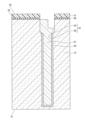
- FIG. 1 is a diagram showing an overall configuration of a solid-state imaging device according to a first embodiment.
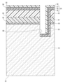
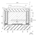
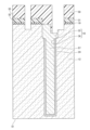
- 2 is a diagram showing a cross-sectional configuration of the solid-state imaging device taken along line AA in FIG. 1.
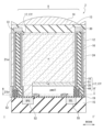
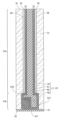
- 5 is a diagram showing the cross-sectional configuration of the solid-state imaging device taken along line C-C' in FIG. 4.
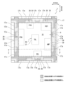
- 3 is a diagram showing a cross-sectional configuration of the solid-state imaging device taken along line B-B' in FIG. 2.
- FIG. 2 is a cross-sectional view showing a one-sided solid-phase diffusion-less portion.
- FIG. 2 is a cross-sectional view showing a solid-phase diffusion-less portion on both sides.
- FIG. 2 is a cross-sectional view showing a portion containing impurity layers on both sides.
- FIG. 11A and 11B are diagrams illustrating two-sided solid-phase diffusion holders of a solid-state imaging device according to a comparative example.
- 11 is a diagram showing a one-side impurity layer-less portion of a solid-state imaging device according to a comparative example.
- FIG. 1A to 1C are diagrams illustrating a method for forming a one-sided solid-phase diffusion-less portion.
- 1A to 1C are diagrams illustrating a method for forming a one-sided solid-phase diffusion-less portion.
- 1A to 1C are diagrams illustrating a method for forming a one-sided solid-phase diffusion-less portion.
- 1A to 1C are diagrams illustrating a method for forming a one-sided solid-phase diffusion-less portion.
- 1A to 1C are diagrams illustrating a method for forming a one-sided solid-phase diffusion-less portion.
- 1A to 1C are diagrams illustrating a method for forming a one-sided solid-phase diffusion-less portion.
- 1A to 1C are diagrams illustrating a method for forming a one-sided solid-phase diffusion-less portion.
- 1A to 1C are diagrams illustrating a method for forming a one-sided solid-phase diffusion-less portion.
- 1A to 1C are diagrams illustrating a method for forming a one-sided solid-phase diffusion-less portion.
- 1A to 1C are diagrams illustrating a method for forming a one-sided solid-phase diffusion-less portion.
- 1A to 1C are diagrams illustrating a method for forming a one-sided solid-phase diffusion-less portion.
- 1A to 1C are diagrams illustrating a method for forming a one-sided solid-phase diffusion-less portion.
- 1A to 1C are diagrams illustrating a method for forming both-side solid-phase diffusion-less portions.
- 1A to 1C are diagrams illustrating a method for forming both-side solid-phase diffusion-less portions.
- 1A to 1C are diagrams illustrating a method for forming both-side solid-phase diffusion-less portions.
- 1A to 1C are diagrams illustrating a method for forming both-side solid-phase diffusion-less portions.
- 1A to 1C are diagrams illustrating a method for forming both-side solid-phase diffusion-less portions.
- 1A to 1C are diagrams illustrating a method for forming both-side solid-phase diffusion-less portions.
- 1A to 1C are diagrams illustrating a method for forming both-side solid-phase diffusion-less portions.
- 1A to 1C are diagrams illustrating a method for forming both-side solid-phase diffusion-less portions.
- 1A to 1C are diagrams illustrating a method for forming a double-sided impurity layer containing portion.
- FIG. 13 is a diagram showing a cross-sectional configuration of a solid-state imaging device according to a first modified example.
- FIG. 13 is a diagram showing a cross-sectional configuration of a solid-state imaging device according to a first modified example.
- FIG. 13 is a diagram showing a cross-sectional configuration of a solid-state imaging device according to a second modified example. This figure shows the cross-sectional configuration of a solid-state imaging device when broken along line D-D' in Figure 32. A cross-sectional view showing the protrusion within a pixel when broken along line E-E' in Figure 32.
- FIG. 13 is a diagram showing a cross-sectional configuration of a solid-state imaging device according to a modified example (3). This figure shows the cross-sectional configuration of the solid-state imaging device when cut along line F-F' in Figure 35.
- FIG. 13 is a diagram showing a cross-sectional configuration of a solid-state imaging device according to a fourth modified example.
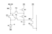
- FIG. 1 is a diagram showing an equivalent circuit of a LOFIC type pixel.
- FIG. 13 is a diagram showing a cross-sectional configuration of a solid-state imaging device according to a modification (5).
- FIG. 13 is a diagram showing a cross-sectional configuration of a solid-state imaging device according to a sixth modified example.
- FIG. 13 is a diagram showing a cross-sectional configuration of a solid-state imaging device according to a second embodiment. This figure shows the cross-sectional configuration of the solid-state imaging device when cut along line H-H' in Figure 42.
- FIG. 44 is a view of a portion of the trench isolation structure surrounding one photoelectric conversion unit shown in FIG. 43, viewed from an oblique direction.
- FIG. 2 is a cross-sectional view showing a one-sided fixed charge-less portion.
- FIG. 4 is a cross-sectional view showing a both-side fixed charge-free portion.
- FIG. 2 is a cross-sectional view showing a fixed charge retaining portion on both sides.
- 1A to 1C are diagrams illustrating a method for forming a one-sided fixed charge-less portion.
- 1A to 1C are diagrams illustrating a method for forming a one-sided fixed charge-less portion.
- 1A to 1C are diagrams illustrating a method for forming a one-sided fixed charge-less portion.
- 1A to 1C are diagrams illustrating a method for forming a one-sided fixed charge-less portion.
- 1A to 1C are diagrams illustrating a method for forming a one-sided fixed charge-less portion.
- 1A to 1C are diagrams illustrating a method for forming a one-sided fixed charge-less portion.
- 1A to 1C are diagrams illustrating a method for forming a one-sided fixed charge-less portion.
- 1A to 1C are diagrams illustrating a method for forming a one-sided fixed charge-less portion.
- 1A to 1C are diagrams illustrating a method for forming a one-sided fixed charge-less portion.
- 1A to 1C are diagrams illustrating a method for forming a one-sided fixed charge-less portion.
- 1A to 1C are diagrams illustrating a method for forming a one-sided fixed charge-less portion.
- 1A to 1C are diagrams illustrating a method for forming a one-sided fixed charge-less portion.
- 1A to 1C are diagrams illustrating a method for forming a one-sided fixed charge-less portion.
- 1A to 1C are diagrams illustrating a method for forming a one-sided fixed charge-less portion.
- 1A to 1C are diagrams illustrating a method for forming a one-sided fixed charge-less portion.
- 1A to 1C are diagrams illustrating a method for forming a one-sided fixed charge-less portion.
- 1A to 1C are diagrams illustrating a method for forming a one-sided fixed charge-less portion.
- 1A to 1C are diagrams illustrating a method for forming a one-sided fixed charge-less portion.
- FIG. 13 is a diagram showing a cross-sectional configuration of a one-sided fixed-charge-less portion according to a first modified example;
- FIG. 13 is a diagram showing a cross-sectional configuration of a one-sided fixed-charge-less portion according to a first modified example;
- FIG. 13 is a diagram showing a cross-sectional configuration of a one-sided fixed-charge-less portion according to a first modified example;
- FIG. 13 is a diagram showing a cross-sectional configuration of a one-sided fixed-charge-less portion according to a second modified example;
- FIG. 13 is a diagram showing a cross-sectional configuration of a one-sided fixed-charge-less portion according to a second modified example;
- FIG. 13 is a diagram showing a cross-sectional configuration of a one-sided fixed-charge-less portion according to a second modified example;
- FIG. 13 is a diagram showing a cross-sectional configuration of a one-sided fixed-charge-less portion according to a second
- FIG. 13 is a diagram showing a cross-sectional configuration of a one-sided fixed-charge-less portion according to a second modified example;
- FIG. 13 is a diagram showing a cross-sectional configuration of a one-sided fixed-charge-less portion according to a modified example (3).
- FIG. 13 is a diagram showing a schematic configuration of an electronic device according to a third embodiment.
- FIG. 13 is a diagram showing a schematic configuration of an electronic device according to a third embodiment.
- First embodiment solid-state imaging device 1-1 Overall configuration of solid-state imaging device 1-2 Configuration of main parts 1-3 Method for forming trench isolation structure 1-4 Modification 2. Second embodiment: solid-state imaging device 2-1 Configuration of main parts 2-2 Method for forming trench isolation structure 2-3 Modification 3. Third embodiment: Application to electronic device
- FIG. 1 is a diagram showing an overall configuration of the solid-state imaging device 1 according to the first embodiment.
- the solid-state imaging device 1 in Fig. 1 is a back-illuminated CMOS (Complementary Metal Oxide Semiconductor) image sensor. As shown in Fig.
- CMOS Complementary Metal Oxide Semiconductor
- the solid-state imaging device 1 (1002) captures image light (incident light) from a subject via a lens group 1001, converts the amount of incident light focused on an imaging surface into an electrical signal on a pixel-by-pixel basis, and outputs the electrical signal.
- the solid-state imaging device 1 includes a pixel region 2, a vertical drive circuit 3, a column signal processing circuit 4, a horizontal drive circuit 5, an output circuit 6, and a control circuit .
- Fig. 2 and Fig. 3 show an example in which two types of pixels 8, large pixels 8a and small pixels 8b, are arranged.
- the large pixels 8a have an L-shaped planar shape obtained by removing one corner from a square, and are arranged in the row and column directions of the pixel region 2.
- the small pixels 8b are formed in a smaller size than the large pixels 8a in the area of the removed corner of the large pixels 8a.
- the small pixels 8b have a square planar shape, and are arranged in the row and column directions of the pixel region 2.
- the small pixels 8b are low-sensitivity pixels having a lower light receiving sensitivity than the large pixels 8a.
- a pixel signal obtained from the large pixels 8a and a pixel signal obtained from the small pixels 8b are combined to express a wide dynamic range.
- the pixels 8 (large pixel 8a, small pixel 8b) have a photoelectric conversion unit 16 (see FIGS. 2 and 3) and a plurality of pixel transistors (for example, a transfer transistor TGL, a reset transistor RST, an amplification transistor AMP, and a selection transistor SEL).
- the vertical drive circuit 3 is configured, for example, by a shift register, and sequentially selects each pixel 8 in the pixel region 2 on a row-by-row basis by, for example, sequentially outputting selection pulses to pixel drive wirings 9, and outputs pixel signals of the selected pixels 8 to the column signal processing circuit 4 through vertical signal lines 10.
- the pixel signals are signals obtained from charges (for example, electrons) generated in the photoelectric conversion units 16.
- the column signal processing circuit 4 is arranged, for example, for each column of pixels 8, and performs signal processing such as noise removal for each pixel column on signals output from one row of pixels 8. For example, correlated double sampling (CDS) for removing fixed pattern noise specific to each pixel and AD (Analog-Digital) conversion can be used as the signal processing.
- the horizontal drive circuit 5 is, for example, composed of a shift register, and sequentially outputs horizontal scanning pulses to the column signal processing circuits 4, selects the column signal processing circuits 4 in order, and causes the selected column signal processing circuit 4 to output pixel signals that have been subjected to signal processing to the horizontal signal line 11.
- the output circuit 6 performs various signal processing on each of the pixel signals sequentially output from the column signal processing circuit 4 through the horizontal signal line 11.
- various types of digital signal processing such as buffering, black level adjustment, column variation correction, etc. can be used.
- the control circuit 7 generates clock signals and control signals that serve as a reference for the operation of the vertical drive circuit 3, the column signal processing circuit 4, the horizontal drive circuit 5, etc., based on a vertical synchronization signal, a horizontal synchronization signal, and a master clock signal (not shown). Then, the control circuit 7 outputs the generated clock signals and control signals to the vertical drive circuit 3, the column signal processing circuit 4, the horizontal drive circuit 5, etc.
- FIG. 2 is a diagram showing a cross-sectional configuration of the solid-state imaging device 1 when cut along the line A-A' in Fig. 1.
- Fig. 2 is also a diagram showing a cross-sectional configuration of the solid-state imaging device 1 when cut along the line A-A' in Fig. 4.
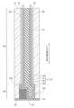
- Fig. 3 is a diagram showing a cross-sectional configuration of the solid-state imaging device 1 when cut along the line CC' in Fig. 4.
- the solid-state imaging device 1 has a semiconductor substrate 12, and a planarization film 13 and on-chip lenses 14 are laminated in this order on a light-receiving surface (hereinafter also referred to as "rear surface S1"; in a broader sense, “first surface”) of the semiconductor substrate 12.
- a color filter or the like may be disposed between the planarization film 13 and the on-chip lenses 14.
- a wiring layer 15 is disposed on the surface (hereinafter also referred to as "front surface S2"; in a broad sense, “second surface”) of the semiconductor substrate 12 opposite to the rear surface S1.
- the semiconductor substrate 12 is a substrate made of silicon (Si) or the like.
- each region corresponding to each pixel 8 (large pixel 8a, small pixel 8b) forms a photoelectric conversion unit 16. That is, a plurality of photoelectric conversion units 16 are arranged in a two-dimensional array on the semiconductor substrate 12.
- the photoelectric conversion unit 16 has a p-type semiconductor region and an n-type semiconductor region, and the pn junction of these semiconductor regions forms a photodiode, generating electric charge according to the amount of received light.
- the photoelectric conversion unit 16 also accumulates electric charge generated by photoelectric conversion in electrostatic capacitance generated at the pn junction.
- a p-well region pwell is formed in a region on the surface S2 side of the semiconductor substrate 12.
- an element isolation region STI for isolating pixel transistors and the like, and pixel transistors (transfer transistor 26 and specified transistor 28 described later) are formed.
- An oxide film for example, can be used as a material for the element isolation region STI.
- Gate electrodes 27 and 29 of the pixel transistors are disposed on the surface S2 via an insulating layer 19.
- the trench isolation structure 17 is formed in the entire region between the adjacent photoelectric conversion units 16 in the semiconductor substrate 12. That is, the trench isolation structure 17 is formed in a lattice shape in the semiconductor substrate 12 so as to surround each of the multiple photoelectric conversion units 16.
- the trench isolation structure 17 is formed so as to penetrate the semiconductor substrate 12 from the back surface S1 to the front surface S2 of the semiconductor substrate 12.
- the trench isolation structure 17 has a trench portion 18, and an insulating layer 19 and a filling material 20 arranged in the trench portion 18.
- the trench portion 18 penetrates the semiconductor substrate 12 from the back surface S1 to the front surface S2 of the semiconductor substrate 12, and the side wall surface forms the outer shape of the trench isolation structure 17.
- the insulating layer 19 covers the inner wall surface of the trench portion 18.
- the trench isolation structure 17 can suppress the movement of charges from one side to the other side between the adjacent photoelectric conversion units 16, and can suppress color mixing.
- the insulating layer 19 may be made of, for example, silicon oxide (SiO 2 ).
- the filler 20 is disposed in the space covered by the insulating layer 19 in the trench portion 18.
- the filler 20 may be made of, for example, polysilicon (p-Si).
- An oxide film 44 may be disposed in the portion of the space covered by the insulating layer 19 on the surface S2 side.
- the oxide film 44 may be made of, for example, silicon oxide (SiO 2 ).
- the trench isolation structure 17 includes three types of trench isolation structures 17 (hereinafter also referred to as "one-side solid-phase diffusion-less portion 17a", “two-side solid-phase diffusion-less portion 17b” and “two-side impurity layer-containing portion 17c") having different shapes, etc.
- Each of the one-side solid-phase diffusion-less portion 17a, the two-side solid-phase diffusion-less portion 17b and the two-side impurity layer-containing portion 17c includes a portion on the back surface S1 side of the semiconductor substrate 12 (hereinafter also referred to as "first trench isolation structure 21a") and a portion on the front surface S2 side (hereinafter also referred to as "second trench isolation structure 21b").
- first trench isolation structure 21a the back surface S1 side of the semiconductor substrate 12
- second trench isolation structure 21b a portion on the front surface S2 side
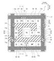
- FIG. 4 is a diagram showing the cross-sectional configuration of the solid-state imaging device 1 when broken along line B-B' in FIG. 2.
- the sidewall having the solid-phase diffusion layer 24 or the impurity layer 25 is represented by high-density dots
- the sidewall not having the solid-phase diffusion layer 24 or the impurity layer 25 is represented by low-density dots.
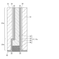
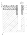
- FIG. 5 is a cross-sectional view showing the one-side solid-phase diffusion-less portion 17a.
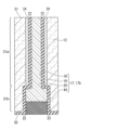
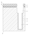
- FIG. 6 is a cross-sectional view showing the both-side solid-phase diffusion-less portion 17b.
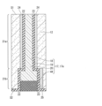
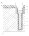
- FIG. 7 is a cross-sectional view showing the both-side impurity layer-containing portion 17c. Note that other components such as pixel transistors are omitted in FIGS. 5, 6, and 7.
- the two sidewalls facing opposite each other have different ranges in the depth direction of the trench portion 18 where the solid-phase diffusion layer 24 is located.
- one of the two sidewalls (the left sidewall in FIG. 5) will be referred to as the "first sidewall 22," and the other sidewall (the right sidewall in FIG. 5) will be referred to as the "second sidewall 23.”
- the solid-phase diffusion layer 24 covering the first sidewall 22 covers only the portion of the first sidewall 22 on the back surface S1 side
- the solid-phase diffusion layer 24 covering the second sidewall 23 covers the entire second sidewall 23.
- the one-side solid-phase diffusion-less portion 17a has a p-type solid-phase diffusion layer 24 on each of the first side wall 22 and the second side wall 23 so as to cover only the portion of the first side wall 22 on the back surface S1 side and to cover the entire second side wall 23.
- the surface S2 side of the one-side solid-phase diffusion-less portion 17a has a structure in which the solid-phase diffusion layer 24 is only on the second side wall 23 side and is not on the first side wall 22 side.
- the solid-phase diffusion layer 24 is a semiconductor region into which a p-type impurity (e.g., boron (B)) is introduced by solid-phase diffusion from the trench portion 18 of the trench isolation structure 17.
- a p-type impurity e.g., boron (B)
- the first side wall 22 of the second trench isolation structure 21b protrudes outward in the width direction of the second trench isolation structure 21b beyond the first side wall 22 of the first trench isolation structure 21a.
- the second sidewall 23 of the second trench isolation structure 21b and the second sidewall 23 of the first trench isolation structure 21a are located in the same plane.
- the solid-phase diffusion layer 24 covers only the first sidewall 22 of the first trench isolation structure 21a and continuously covers the second sidewalls 23 of the first trench isolation structure 21a and the second trench isolation structure 21b.
- the both-side solid-phase diffusion-less portion 17b has a p-type solid-phase diffusion layer 24 on the first side wall 22 and the second side wall 23 so as to cover only the back surface S1 side of each of the two side walls (first side wall 22 and second side wall 23) facing opposite to each other.
- the surface S2 side of the both-side solid-phase diffusion-less portion 17b has a structure in which there is no solid-phase diffusion layer 24 on either the first side wall 22 side or the second side wall 23 side.
- the first side wall 22 of the second trench isolation structure 21b protrudes outward in the width direction of the second trench isolation structure 21b beyond the first side wall 22 of the first trench isolation structure 21a.
- the second side wall 23 of the second trench isolation structure 21b protrudes outward in the width direction of the second trench isolation structure 21b beyond the second side wall 23 of the first trench isolation structure 21a.
- the solid-phase diffusion layer 24 covers the first sidewall 22 and the second sidewall 23 of the first trench isolation structure 21a.
- the both-side impurity layer holding portion 17c has a p-type solid-phase diffusion layer 24 on the first side wall 22 and the second side wall 23 so as to cover the back surface S1 side of each of the two side walls (first side wall 22, second side wall 23) facing opposite to each other, and further has a p-type impurity layer 25 on the first side wall 22 and the second side wall 23 so as to cover the surface S2 side.
- the surface S2 side of the both-side impurity layer holding portion 17c has a structure in which the impurity layer 25 is provided on both the first side wall 22 side and the second side wall 23 side.
- the both-side impurity layer holding portion 17c has a structure in which the first side wall 22 and the second side wall 23 of the second trench isolation structure 21b of the both-side solid-phase diffusion-less portion 17b are covered with the impurity layer 25.
- the impurity layer 25 is a semiconductor region into which a p-type impurity (e.g., boron (B)) is introduced by ion implantation.
- the one-side solid-phase diffusion-less portion 17a, the both-side solid-phase diffusion-less portion 17b, and the both-side impurity layer holding portion 17c are used in each portion of the trench isolation structure 17.
- the one-side solid-phase diffusion-less portion 17a is used in a portion of the trench isolation structure 17 located near the transfer transistor 26, and is arranged so that the solid-phase diffusion layer 24 (see FIG. 5) is located on the sidewall side near the gate electrode 27 of the transfer transistor 26.
- the gate electrode 27 for example, a flat surface electrode formed on the surface S2 side of the semiconductor substrate 12, or a vertical electrode reaching a predetermined depth from the surface S2 can be adopted.
- the sidewall near the gate electrode 27 can be made to have a high hole concentration, and the pinning of the sidewall can be strengthened near the gate electrode 27. Therefore, for example, when the charge of the photoelectric conversion unit 16 is transferred by the gate electrode 27, the inclusion of dark current 8 into the transferred charge can be reduced.
- the solid-phase diffusion layer 24 (see FIG. 5) is used to strengthen the pinning of the sidewall, the expansion of the diffusion range of the p-type impurity can be suppressed compared to the case where, for example, the impurity layer 25 (see FIG.
- FIG. 4 illustrates an example in which, when viewed from the thickness direction of the semiconductor substrate 12, the gate electrode 27 of the transfer transistor 26 is disposed near the L-shaped corner of the large pixel 8a, and a one-sided solid-phase diffusion-less portion 17a is used for the trench isolation structure 17 near the gate electrode 27.
- the one-sided solid-phase diffusion-less portion 17a is disposed such that the second sidewall 23 side shown in FIG. 5 faces the gate electrode 27 side.
- the one-side solid-phase diffusion-less portion 17a and the both-side solid-phase diffusion-less portion 17b are used in a portion of the trench isolation structure 17 located near a pixel transistor (hereinafter also referred to as a "predetermined transistor 28") other than the transfer transistor 26, and are arranged so that the solid-phase diffusion layer 24 and the impurity layer 25 do not overlap the gate electrode 29 of the predetermined transistor 28.
- a predetermined transistor 28 pixel transistor
- the solid-phase diffusion layer 24 and the impurity layer 25 are formed so that the solid-phase diffusion layer 24 does not overlap the gate electrode 29 of the predetermined transistor 28, and the impurity layer 25 does not overlap the gate electrode 29 of the predetermined transistor 28, when viewed from the thickness direction of the semiconductor substrate 12.
- the predetermined transistor 28 include a reset transistor RST, an amplification transistor AMP, and a selection transistor SEL (see FIG. 4).
- a flat surface electrode formed on the surface S2 side of the semiconductor substrate 12 can be used as the gate electrode 29.
- the pinning layer By not forming the pinning layer at a position overlapping the gate electrode 29, it is possible to suppress interference of the pinning layer with the channel formation region at a position facing the gate electrode 29, and suppress deterioration of the function of the predetermined transistor 28. Therefore, it is not necessary to arrange the predetermined transistor 28 away from the sidewall of the trench isolation structure 17, and it is possible to suppress deterioration of the area efficiency in the pixel.
- the one-sided solid-phase diffusion-less portion 17a a structure is formed in which the solid-phase diffusion layer 24 is provided on the sidewall opposite to the sidewall overlapping with the gate electrode 29, so that the opposite sidewall can be brought into a high hole concentration state, and the pinning of the opposite sidewall can be strengthened.
- the both-side impurity layer containing portion 17c is used in a portion of the trench isolation structure 17 other than the one-side solid-phase diffusion-less portion 17a and the both-side solid-phase diffusion-less portion 17b. That is, the both-side impurity layer containing portion 17c is disposed at a position away from the pixel transistors (transfer transistor 26, specified transistor 28).
- the impurity layer 25 of the both-side impurity layer containing portion 17c can put the sidewall of the trench isolation structure 17 into a high hole concentration state, and the pinning can be further strengthened.
- the planarization film 13 continuously covers the rear surface S1 of the semiconductor substrate 12 so that the rear surface S1 is flat.
- materials that can be used for the planarization film 13 include silicon oxide ( SiO2 ) and silicon nitride (SiN).
- a light-shielding film 30 is disposed in the planarization film 13, and has an opening in a portion facing the photoelectric conversion unit 16, and shields the region between the photoelectric conversion units 16 from light.
- Examples of materials that can be used for the light-shielding film 30 include tungsten (W) and aluminum (Al).
- the on-chip lenses 14 are arranged in a two-dimensional array such that one on-chip lens 14 is arranged for one photoelectric conversion unit 16.
- the on-chip lens 14 collects light from a subject and causes the collected light to enter the photoelectric conversion unit 16 via the planarization film 13.
- the wiring layer 15 has an interlayer insulating film (not shown) and wiring (not shown) stacked in multiple layers with the interlayer insulating film interposed therebetween, and drives the pixel transistors of each pixel 8 via the multiple layers of wiring.
- the solid-state imaging device 1 having the above configuration, light is incident from the rear surface S1 side of the semiconductor substrate 12, passes through the on-chip lens 14, and the transmitted light is photoelectrically converted in the photoelectric conversion unit 16 to generate electric charges (e.g., electrons). The generated electric charges are then output as pixel signals from the vertical signal lines 10 (see FIG. 1) formed by the wiring of the wiring layer 15. Furthermore, the solid-state imaging device 1 according to the first embodiment can express a wide dynamic range by combining pixel signals obtained from the large pixels 8a and the small pixels 8b.
- electric charges e.g., electrons
- a two-sided solid-phase diffusion holding portion 17d is used in which the entire first side wall 22 of the one-sided solid-phase diffusion-less portion 17a shown in FIG. 5 is made flat and a solid-phase diffusion layer 24 is disposed on the entire flat surface.
- the solid-phase diffusion layer 24 is present on the entire first side wall 22 and second side wall 23, the pinning of the side walls can be strengthened.
- solid-phase diffusion layer 24 interferes with the pixel transistor (prescribed transistor 28), the operating characteristics of the pixel transistor may change, so the pixel transistor and the side wall (solid-phase diffusion layer 24) need to be disposed apart, which may reduce area efficiency.
- At least a part (one-sided solid-phase diffusion-less portion 17a) of the trench isolation structure 17 is configured to have a p-type solid-phase diffusion layer 24 on each of the first sidewall 22 and the second sidewall 23, so that only the back surface S1 side portion of the first sidewall 22 is covered and the entire second sidewall 23 is covered, out of the two sidewalls (first sidewall 22, second sidewall 23) facing opposite to each other. Therefore, since the solid-phase diffusion layer 24 is present on the surface S2 side of the second sidewall 23, the pinning on the surface S2 side of the second sidewall 23 can be strengthened.
- the solid-phase diffusion layer 24 since there is no solid-phase diffusion layer 24 on the surface S2 side of the first sidewall 22, the solid-phase diffusion layer 24 does not affect the operating characteristics of the pixel transistor (predetermined transistor 28) on the surface S2 side of the first sidewall 22, and since there is no restriction on the distance between the pixel transistor and the sidewall, etc., a decrease in area efficiency can be suppressed.
- a one-sided impurity layer-less portion 17e in which the impurity layer 25 of the first sidewall 22 of the both-sided impurity layer holding portion 17c shown in FIG. 7 is omitted is used as shown in FIG. 9.
- the impurity layer 25 is formed by introducing p-type impurities from the surface S2 side by ion implantation after forming pixel transistors in the semiconductor substrate 12. Therefore, for example, when the one-sided impurity layer-less portion 17e is disposed near the transfer transistor 26 (the portion of the one-sided solid-phase diffusion-less portion 17a in the upper left corner in FIG.
- the transfer transistor 26 may prevent the introduction of impurities because the interval between the transfer transistor 26 and the sidewall of the one-sided impurity layer-less portion 17e is narrow. Also, the impurity concentration of the impurity layer 25 may vary due to the variation in the shape of the trench portion 18, which may cause the pinning to vary. Furthermore, if the impurity concentration of the impurity layer 25 is increased in order to prevent variations in pinning, there is a possibility that the charge transfer by the transfer transistor 26 may deteriorate.
- the solid-phase diffusion layer 24 is used to strengthen the pinning of the sidewall of the one-side solid-phase diffusion-less portion 17a, even if the distance between the transfer transistor 26 and the sidewall of the one-side solid-phase diffusion-less portion 17a is narrow, the introduction of impurities for forming the impurity layer 25 is not hindered. In addition, it is possible to suppress the variation in the impurity concentration of the solid-phase diffusion layer 24 due to the variation in the shape of the trench portion 18, and thus it is possible to suppress the variation in pinning.
- a method for forming the one-side solid-phase diffusion-less portion 17a will be described.
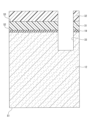
- a semiconductor substrate 12 is prepared in which a part of the insulating layer 19 and a protective film 31 (e.g., a silicon nitride film) are laminated in this order on the surface S2 of the semiconductor substrate 12.
- a mask 32 e.g., a TEOS film
- the second trench isolation structure 21b see FIG. 5
- etching is performed through the mask 32 to remove a part of the insulating layer 19 and the protective film 31 to expose the surface S2 of the semiconductor substrate 12.
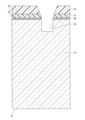
- etching is performed through the mask 32 to form a second trench portion 33 that forms the outer shape of the second trench isolation structure 21b (see FIG. 5) of the one-side solid-phase diffusion-less portion 17a.
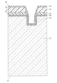
- a sidewall film 34 is formed so as to continuously cover the upper surface S4 of the mask 32 and the inner wall surface of the second trench portion 33.
- the sidewall film 34 is composed of a silicon oxide (SiO 2 ) film 35 , a silicon nitride (SiN) film 36 and an ISSG (In-situ Steam Generation) film 37 .
- a mask 38 having an opening is formed on the upper surface S5 side of the sidewall film 34 at the position of the sidewall film 34 covering one of the inner wall surfaces of the second trench portion 33 (the inner wall surface on the left side in FIG. 13.
- second inner wall surface S6 also referred to as the "second inner wall surface S6"
- etching is performed through the mask 38 to remove the sidewall film 34 from the second inner wall surface S6 and expose the second inner wall surface S6.
- FIG. 14 after removing the mask 38, etching is performed using the sidewall film 34 covering the other inner wall surface of the second trench portion 41 (the inner wall surface on the right side in FIG. 14.
- first inner wall surface S7 also referred to as the "first inner wall surface S7" as a mask to form a first trench portion 39 that forms the outer shape of the second trench isolation structure 21b (see FIG. 5) of the one-sided solid-phase diffusion-less portion 17a.
- a BSG (Boro-Silicate Glass) film 40 is formed so as to continuously cover the upper surface S4 of the mask 32, the surface of the sidewall film 34, the second inner wall surface S6 of the first trench portion 39 and the second trench portion 33, and the first inner wall surface S7 of the first trench portion 39.
- the BSG film 40 etc.
- p-type impurities boron (B)
- B p-type impurities
- the BSG film 40 is peeled off from the upper surface S4 of the mask 32, etc.
- the sidewall film 34 is peeled off from the inner wall surface of the second trench portion 33.
- the mask 32 TEOS film
- the remaining part of the insulating layer 19 is formed so as to continuously cover the inner wall surfaces of the first trench portion 39 and the second trench portion 33.
- the filler 20 is embedded in the space covered by the insulating layer 19.
- the filling material 20 is embedded until the filler 20 covers the entire upper surface S3 of the protective film 31.
- an etch-back is performed to remove the filler 20 from the upper surface S3 of the protective film 31.
- the same procedure as in the method for forming the one-side solid-phase diffusion-free portion 17a is performed up to the formation of the sidewall film 34 shown in FIG. 12.
- the trench portion forming the outer shape of the second trench isolation structure 21b (see FIG. 6) of the both-side solid-phase diffusion-free portion 17b is indicated as the "second trench portion 41".
- etching is performed using the portion of the sidewall film 34 covering the second trench portion 41 as a mask, and as shown in FIG. 22, a first trench portion 42 forming the outer shape of the first trench isolation structure 21a (see FIG.
- a BSG film 40 is formed so as to continuously cover the upper surface S4 of the mask 32, the surface of the sidewall film 34, and the inner wall surface of the first trench portion 42.
- the BSG film 40 and the like are heated in a diffusion furnace, and p-type impurities (boron (B)) are diffused from the BSG film 40 toward the inner wall surface of the first trench portion 42, as shown in Fig. 24.
- the p-type impurity is not diffused.
- p-type solid-phase diffusion layers 24 are formed in each of the two inner wall surfaces of the first trench portion 42. After the solid-phase diffusion layers 24 are formed, the BSG film 40 is peeled off from the upper surface S4 of the mask 32 and the like.
- the sidewall film 34 is peeled off from the inner wall surface of the second trench portion 33.
- the mask 32 TEOS film
- the remaining part of the insulating layer 19 is formed so as to continuously cover the inner wall surfaces of the first trench portion 42 and the second trench portion 33.
- the filler 20 is embedded in the space covered by the insulating layer 19. The embedding of the filler 20 is performed until the filler 20 covers the entire upper surface S3 of the protective film 31.
- an etch-back is performed to remove the filler 20 from the upper surface S3 of the protective film 31.
- both-side impurity layer containing portion 17c a method for forming the both-side impurity layer containing portion 17c will be described.
- the same procedure as in the method for forming the both-side solid-phase diffusion-less portion 17b is performed up to the removal of the filling material 20 shown in Fig. 29.
- p-type impurities e.g., boron (B)
- B boron
- the one-side solid-phase diffusion-less portion 17a, the both-side solid-phase diffusion-less portion 17b, and the both-side impurity layer holding portion 17c differ only in the configuration of the second trench isolation structure 21b (second trench portions 33, 41), and therefore can be formed without increasing the number of steps, and are relatively easy to form.
- FIG. 4 an example is shown in which the one-side solid-phase diffusion-less portion 17a or the both-side solid-phase diffusion-less portion 17b is arranged so that the pinning layer (solid-phase diffusion layer 24, impurity layer 25) does not overlap the gate electrode 29 of the pixel transistor (predetermined transistor 28), but other configurations can also be adopted.
- a configuration in which only the both-side impurity layer holding portion 17c is arranged in a portion located near the predetermined transistor 28 may be used.
- FIG. 31 illustrates a case in which the one-side solid-phase diffusion-less portion 17a is used only in a portion of the trench isolation structure 17 located near the transfer transistor 26.
- FIG. 4 an example in which the pinning layer (solid-phase diffusion layer 24, impurity layer 25) is disposed only on the side wall of the trench isolation structure 17 is shown, but other configurations can also be adopted.
- a pixel protrusion 43 protruding from the trench isolation structure 17 into a region of the semiconductor substrate 12 surrounded by the trench isolation structure 17 may be formed, and a solid-phase diffusion layer 48 may be disposed around the formed pixel protrusion 43.
- FIG. 33 illustrates a case in which the pixel protrusion 43 protrudes from the second trench isolation structure 21b into the p-well region pwell.
- the pixel protrusion 43 has a trench portion 45, and an insulating layer 46 and an oxide film 47 disposed in the trench portion 45.
- the trench portion 45 reaches a predetermined depth in the semiconductor substrate 12 from the surface S2 of the semiconductor substrate 12, and the sidewall surface forms the outline of the pixel protrusion 43.
- the insulating layer 46 covers the sidewall and bottom surfaces of the trench portion 45.
- the insulating layer 46 is formed integrally with the insulating layer 19 of the trench isolation structure 17.
- the insulating layer 46 may be made of, for example, the same material (SiO 2 or the like) as the insulating layer 19.
- the oxide film 47 is disposed in the space covered by the insulating layer 46 in the trench portion 45.
- the oxide film 47 is formed integrally with the insulating layer 19 of the trench isolation structure 17.
- the oxide film 47 may be made of, for example, the same material (SiO 2 or the like) as the insulating layer 19.
- a p-type solid-phase diffusion layer 48 is formed around the pixel protrusion 43, continuously covering the side and bottom surfaces of the pixel protrusion 43.
- the solid-phase diffusion layer 48 is a semiconductor region into which p-type impurities (for example, boron (B)) are introduced by solid-phase diffusion.
- the solid-phase diffusion layer 48 of the intra-pixel protrusion 43 can bring the area around the intra-pixel protrusion 43 into a high hole concentration state, thereby strengthening pinning.
- Fig. 34 is a cross-sectional view showing the intra-pixel protrusion 43 when cut along the line E-E' in Fig. 32.
- each pixel 8 in the pixel region 2 includes two or more types of pixels 8 of different sizes, such as large pixels 8a and small pixels 8b, but other configurations can also be adopted.
- each pixel 8 in the pixel region 2 may include only pixels 8 of the same size.
- Fig. 36 is a diagram showing the cross-sectional configuration of the solid-state imaging device 1 when broken along line F-F' in Fig. 35.
- a configuration may be used that includes LOFIC (Lateral Overflow Integration Capacitor) type pixels 8 that allow charge overflowing from the photoelectric conversion section 16 to overflow and increase the saturated charge amount Qs.
- Figure 38 is a diagram showing the cross-sectional configuration of the solid-state imaging device 1 when broken along line G-G' in Figure 37.
- Figure 38 illustrates an example in which the configuration is applied to a configuration including only pixels 8 of the same size, similar to the above variant example (3).
- the LOFIC type pixel 8 includes a transfer transistor 26 (TGL in FIG.
- the discharge transistor OFG electrically connects the photoelectric conversion unit 16 and the storage capacitance MIM, and the charge overflowing from the photoelectric conversion unit 16 is accumulated in the storage capacitance MIM.
- This configuration of pixel 8 allows the storage capacitance MIM and floating diffusion FD to store charge exceeding the saturation charge amount Qs, expanding the dynamic range.
- FIG. 40 illustrates an example of an application to a configuration including only pixels 8 of the same size, as in the modification (3).
- the pixel 8 of a shared FD type has, on the surface S2 side of the semiconductor substrate 12, multiple transfer transistors 26 that transfer charges photoelectrically converted by the photoelectric conversion units 16, and multiple floating diffusions FD (broadly speaking, "charge storage units") that accumulate the charges transferred by the transfer transistors 26.
- Each of the multiple floating diffusions FD is shared by two or more photoelectric conversion units 16.
- FIG. 40 illustrates an example of a case in which one floating diffusion FD is shared by four photoelectric conversion units 16 arranged in two rows and two columns.
- the solid-state imaging device 1 is configured by stacking the first substrate 100, the second substrate 200, and the third substrate 300 in this order from the light incident surface side of the solid-state imaging device 1.
- the first substrate 100 has a semiconductor substrate 12 having a photoelectric conversion section 16, a transfer transistor 26 that transfers the charge photoelectrically converted by the photoelectric conversion section 16, and a floating diffusion FD (broadly speaking, a "charge accumulation section") that accumulates the charge transferred by the transfer transistor 26.
- the second substrate 200 has a pixel transistor (predetermined transistor 28) that reads out the charge accumulated in the floating diffusion FD.
- pixel transistors (predetermined transistors 28) that read out charges include a reset transistor RST, an amplification transistor AMP, and a selection transistor SEL.
- the third substrate 300 also has a logic circuit 49 that processes pixel signals obtained from the charges read out by the second substrate 200. Examples of the logic circuit 49 include a vertical drive circuit 3, a column signal processing circuit 4, a horizontal drive circuit 5, an output circuit 6, and a control circuit 7 (see FIG. 1).
- a color filter 50 and an on-chip lens 14 are stacked in this order on the light receiving surface (rear surface S1) side of the first substrate 100.
- FIG. 41 illustrates an example in which one color filter 50 and one on-chip lens 14 are arranged for four photoelectric conversion units 16 arranged in a 2 x 2 array. That is, a plurality of on-chip lenses 14 are arranged on the light receiving surface (rear surface S1) side of the semiconductor substrate 12, and each of the plurality of on-chip lenses 14 is shared by two or more photoelectric conversion units 16. By sharing with two or more photoelectric conversion units 16, a phase difference can be detected from the output of the four photoelectric conversion units 16, and autofocus can be performed using the detected phase difference.
- FIG. 42 is a diagram corresponding to FIG. 2 of the first embodiment, and is a diagram showing a cross-sectional configuration of the solid-state imaging device 1 according to the second embodiment when broken along line II' in FIG. 43.
- FIG. 43 is a diagram corresponding to FIG. 4 of the first embodiment, and is a diagram showing a cross-sectional configuration of the solid-state imaging device 1 when broken along line HH' in FIG. 42.
- FIGS. 42 is a diagram corresponding to FIG. 2 of the first embodiment, and is a diagram showing a cross-sectional configuration of the solid-state imaging device 1 according to the second embodiment when broken along line II' in FIG. 43.
- FIG. 43 is a diagram corresponding to FIG. 4 of the first embodiment, and is a diagram showing a cross-sectional configuration of the solid-state imaging device 1 when broken along line HH' in FIG. 42.
- FIGS. 42 and 43 illustrate a case where the pixel 8 is configured to include the discharge transistor OFG and the like shown in FIGS. 37 to 39.
- the gate electrodes of the pixel transistors other than the transfer transistor 26 are configured to overlap the trench isolation structure 17. That is, when viewed from the thickness direction of the semiconductor substrate 12, a partial region of the gate electrode of the pixel transistor is configured to have a region overlapping with the trench isolation structure 17.
- Examples of the pixel transistor include a transfer transistor TGL (hereinafter also referred to as a "transfer transistor 26"), a reset transistor RST, an amplification transistor AMP, a selection transistor SEL, a capacitor control transistor FCG, a capacitor connection transistor FDG, and a discharge transistor OFG.
- a transfer transistor TGL hereinafter also referred to as a "transfer transistor 26”
- a reset transistor RST an amplification transistor AMP
- a selection transistor SEL selection transistor
- FCG capacitor control transistor
- FDG capacitor connection transistor
- OFG discharge transistor
- the solid-state imaging device 1 according to the second embodiment differs from the solid-state imaging device 1 according to the first embodiment in the configuration of the trench isolation structure 17.
- the trench isolation structure 17 of the second embodiment includes three types of trench isolation structures 17 (hereinafter, also referred to as "one-side fixed charge-less portion 17f", “both-side fixed charge-less portion 17g” and “both-side fixed charge holding portion 17h") as shown in Figures 43, 44, 45, 46 and 47.
- Figure 44 is a view of a portion of the trench isolation structure 17 (trench portion 18) surrounding one photoelectric conversion portion 16 shown in Figure 43, viewed from an oblique direction.
- Figure 45 is a cross-sectional view showing the one-side fixed charge-less portion 17f.
- Figure 46 is a cross-sectional view showing the both-side fixed charge-less portion 17g.
- Figure 47 is a cross-sectional view showing the both-side fixed charge holding portion 17h. Note that other configurations such as pixel transistors are omitted in Figures 45, 46 and 47.
- a fixed charge film 51 that covers the inner wall surface of the trench portion 18 and has a negative charge is arranged in the trench portion 18. That is, the trench isolation structure 17 is formed to include a trench portion 18, a fixed charge film 51, and a filling material 20.
- a high refractive index material film or a high dielectric film having a negative charge can be used as the fixed charge film 51.
- an oxide or nitride containing at least one element of hafnium (Hf), aluminum (Al), zirconium (Zr), tantalum (Ta), and titanium (Ti) can be used.
- the configuration of the fixed charge film 51 is different for each type of trench isolation structure 17 (one-side fixed charge-less portion 17f to both-side fixed charge holding portion 17h).
- the outer shapes of the widthwise cross sections of the one-side fixed charge-less portion 17f, the two-side fixed charge-less portion 17g, and the two-side fixed charge holding portion 17h are the same bilaterally symmetrical shapes.
- the width of the second trench isolation structure 21b is wider than the width of the first trench isolation structure 21a.
- the solid-phase diffusion layers 24 of the one-side fixed charge-less portion 17f, the two-side fixed charge-less portion 17g, and the two-side fixed charge holding portion 17h are arranged so as to cover only the first sidewall 22 and the second sidewall 23 of the first trench isolation structure 21a.
- the solid-phase diffusion layer 24 (broadly speaking, the "p-type semiconductor region") is arranged outside the trench isolation structure 17 and covers only the back surface S1 side portions of the two sidewalls of the trench isolation structure 17 facing opposite to each other.
- an insulating material is used as the filler 20 arranged in the trench isolation structure 17 instead of polysilicon (p-Si). Examples of insulating materials include silicon oxide (SiO).
- the two opposing inner wall surfaces have different ranges in the depth direction of the trench portion 18 where the fixed charge film 51 is located.
- one of the two inner wall surfaces (the left inner wall surface in Figure 45) will also be referred to as the "first inner wall surface S8," and the other inner wall surface (the right inner wall surface in Figure 45) will also be referred to as the "second inner wall surface S9.”
- the fixed charge film 51 on the first inner wall surface S8 side covers only the portion of the first inner wall surface S8 on the back surface S1 side.
- the fixed charge film 51 on the second inner wall surface S9 side covers the entire second inner wall surface S9.
- FIG. 45 illustrates a case where the fixed charge film 51 is configured to continuously cover the entire portion of the second inner wall surface S9 constituting the first trench isolation structure 21a and the entire portion of the second trench isolation structure 21b.
- An oxide film 44 is disposed on the surface S2 side and the first inner wall surface S8 side of the space in the trench portion 18 of the one-sided fixed charge-less portion 17f.
- the fixed charge film 51 continuously covers the surface of the oxide film 44 on the back surface S1 side (hereinafter also referred to as "back surface S10"), the surface of the oxide film 44 on the second inner wall surface S9 side (hereinafter also referred to as “side surface S11"), and the portion of the bottom surface S12 of the trench portion 18 between the side surface S11 and the second inner wall surface S9.
- the bottom surface S12 is the surface facing the opening on the surface S2 side of the trench portion 18 (the upper surface of the insulating layer 19 in FIG. 45).
- the first inner wall surface S8 side of the fixed charge film 51 covering the back surface S10 is continuous with the fixed charge film 51 covering the first inner wall surface S8, and the second inner wall surface S9 side of the fixed charge film 51 covering the bottom surface S12 is continuous with the fixed charge film 51 covering the second inner wall surface S9.
- the fixed charge film 51 covering the first inner wall surface S8 and the second inner wall surface S9 has the same range in the depth direction of the trench portion 18.
- the fixed charge film 51 on the first inner wall surface S8 side and the fixed charge film 51 on the second inner wall surface S9 side cover only the back surface S1 side of the first inner wall surface S8 and the second inner wall surface S9.
- FIG. 46 illustrates a case in which the fixed charge film 51 is configured to continuously cover the entire part constituting the first trench isolation structure 21a of each of the first inner wall surface S8 and the second inner wall surface S9 and the end of the part constituting the second trench isolation structure 21b on the first trench isolation structure 21a side.
- an oxide film 44 is arranged in the part on the front surface S2 side of the space in the trench portion 18 of the both-side fixed charge-less portion 17g.
- the fixed charge film 51 also covers the rear surface S10 of the oxide film 44.
- the first inner wall surface S8 side of the fixed charge film 51 covering the rear surface S10 is continuous with the fixed charge film 51 covering the first inner wall surface S8, and the second inner wall surface S9 side is continuous with the fixed charge film 51 covering the second inner wall surface S9.
- the fixed charge film 51 covering the first inner wall surface S8 and the second inner wall surface S9 of the both-side fixed charge holding portion 17h is located in the same range in the depth direction of the trench portion 18 as the both-side fixed charge-less portion 17g. Specifically, in the both-side fixed charge holding portion 17h, the fixed charge film 51 covers the entire first inner wall surface S8 and the second inner wall surface S9.
- FIG. 47 illustrates a case in which the fixed charge film 51 is configured to continuously cover the entire portion of the first inner wall surface S8 and the entire portion of the second trench isolation structure 21b of each of the first inner wall surface S8 and the second inner wall surface S9.
- the fixed charge film 51 covers the bottom surface S12 of the trench portion 18 in addition to the inner wall surfaces.
- the first inner wall surface S8 side of the fixed charge film 51 covering the bottom surface S12 is continuous with the fixed charge film 51 covering the first inner wall surface S8, and the second inner wall surface S9 side is continuous with the fixed charge film 51 covering the second inner wall surface S9.
- the fixed charge holding portion 17h on both sides does not have an oxide film 44.
- each of the one-side fixed charge-less portion 17f, the both-side fixed charge-less portion 17g, and the both-side fixed charge holding portion 17h is used in each portion of the trench isolation structure 17.
- the inner wall surface on the one photoelectric conversion portion 16 side has a range in which the fixed charge film 51 is located in the depth direction of the trench portion 18, which range differs depending on the circumferential position of the one photoelectric conversion portion 16.
- the fixed charge film 51 covering the inner wall surface on the one photoelectric conversion portion 16 side has a portion covering only a portion of the inner wall surface on the back surface S1 side, and a portion covering the entire inner wall surface.
- the one-sided fixed charge-less portion 17f is used in a portion of the trench isolation structure 17 located near the discharge transistor OFG, and is arranged so that the fixed charge film 51 is located on the inner wall surface side close to the gate electrode 52 of the discharge transistor OFG.
- the discharge transistor OFG for example, as shown in FIG. 39, a pixel transistor that electrically connects the photoelectric conversion portion 16 and the storage capacitance MIM and stores the charge overflowing from the photoelectric conversion portion 16 in the storage capacitance MIM can be adopted.
- FIG. 43 illustrates a case where the one-sided fixed charge-less portion 17f is used at a position overlapping the gate electrode 52 of the trench isolation structure 17 when viewed from the thickness direction of the semiconductor substrate 12. Also, in FIG. 43, the one-sided fixed charge-less portion 17f is arranged so that the second inner wall surface S9 side (i.e., the side where the fixed charge film 51 is arranged in the second trench isolation structure 21b) shown in FIG. 45 faces the gate electrode 52 side.
- the second inner wall surface S9 side i.e., the side where the fixed charge film 51 is arranged in the second trench isolation structure 21b
- the discharge transistor OFG has a charge transfer path from the photoelectric conversion section 16 to the discharge transistor OFG. Therefore, for example, when the discharge transistor OFG is formed near the trench isolation structure 17 (trench section 18), there is a possibility that the charge (charge generating dark current) that flows out from the vicinity of the trench section 18 may move into the photoelectric conversion section 16 through the above-mentioned transfer path.
- the sidewall near the gate electrode 52 of the trench isolation structure 17 can be made to have a high hole concentration, and the pinning of the sidewall near the gate electrode 52 of the trench isolation structure 17 can be strengthened.
- the charge (charge generating dark current) that flows out from the vicinity of the trench section 18 can be suppressed, and the intrusion of dark current from the discharge transistor OFG to the photoelectric conversion section 16 can be suppressed.
- a fixed charge film 51 (see FIG. 45) is used to strengthen the pinning of the sidewall near the gate electrode 52, unlike when a semiconductor region (impurity layer) into which p-type impurities are introduced is used, it is possible to prevent the charge transfer path from the photoelectric conversion unit 16 to the emission transistor OFG from narrowing, and also to prevent a reduction in the saturation charge amount Qs.
- the one-sided fixed charge-less portion 17f is also used in a portion of the trench isolation structure 17 located near the element isolation region STI that isolates pixel transistors and the like, and is arranged so that the fixed charge film 51 is located on the inner wall surface side close to the element isolation region STI.
- This allows the sidewall of the trench isolation structure 17 close to the element isolation region STI to have a high hole concentration state, and the pinning of the sidewall near the element isolation region STI can be strengthened. Therefore, the charge (charge generating dark current) that flows out from between the element isolation region STI and the trench isolation structure 17 can be suppressed, and the intrusion of dark current into the photoelectric conversion unit 16 can be suppressed.
- the one-sided fixed charge-less portion 17f is used in a portion of the trench isolation structure 17 that contacts the element isolation region STI when viewed from the thickness direction of the semiconductor substrate 12.
- the one-sided fixed charge-less portion 17f is arranged such that the second inner wall surface S9 side shown in FIG. 45 (the side where the fixed charge film 51 is arranged in the second trench isolation structure 21b) faces the element isolation region STI side.
- a both-side fixed charge retaining portion 17h is used instead of the one-side fixed charge-less portion 17f.
- the one-sided fixed charge-less portion 17f is also used in a portion of the trench isolation structure 17 located near the impurity diffusion region 53 of the pixel transistor, and is arranged so that the oxide film 44 is located on the inner wall surface side close to the impurity diffusion region 53.
- an n+ type semiconductor region functioning as a source region and a drain region can be used as the impurity diffusion region 53.
- FIG. 43 illustrates a case in which the impurity diffusion region 53 is arranged at a position in contact with the one-sided fixed charge-less portion 17f when viewed from the thickness direction of the semiconductor substrate 12. Also, in FIG.
- the one-sided fixed charge-less portion 17f is arranged so that the first inner wall surface S8 side (the side where the oxide film 44 is arranged in the second trench isolation structure 21b) shown in FIG. 45 faces the impurity diffusion region 53 side.
- the fixed charge film 51 is formed near the impurity diffusion region 53, a strong electric field may be generated between the fixed charge film 51 and the impurity diffusion region 53, resulting in white spots. In response to this, as shown in FIG.
- a both-side fixed charge-less portion 17g is used instead of the one-side fixed charge-less portion 17f.
- the both-side fixed charge-less portion 17g is used instead of the one-side fixed charge-less portion 17f.
- the predetermined transistor 54 for example, a pixel transistor other than the discharge transistor OFG and the transfer transistor 26 can be used.
- the gate electrode 55 for example, a flat surface electrode formed on the surface S2 side of the semiconductor substrate 12 can be used.
- the predetermined transistor 54 there is no charge transfer path between the predetermined transistor 54 and the photoelectric conversion portion 16, such as the one that exists between the discharge transistor OFG and the photoelectric conversion portion 16. Therefore, even if the predetermined transistor 54 is formed near the trench isolation structure 17 (trench portion 18), the charge (charge generating a dark current) that flows out from the vicinity of the trench portion 18 does not move into the photoelectric conversion portion 16 through the above-mentioned transfer path.
- At least a part (one-sided fixed charge-less portion 17f) of the trench isolation structure 17 is configured such that the ranges in which the fixed charge film 51 is located are different from each other on two opposing inner wall surfaces (first inner wall surface S8, second inner wall surface S9) in the depth direction of the trench portion 18.
- the fixed charge film 51 covering the first inner wall surface S8 covers only the portion of the first inner wall surface S8 on the back surface S1 side
- the fixed charge film 51 covering the second inner wall surface S9 covers the entire second inner wall surface S9.
- the fixed charge film 51 is present on the surface S2 side of the second inner wall surface S9, the pinning on the surface S2 side of the second inner wall surface S9 can be strengthened. Furthermore, since there is no fixed charge film 51 on the surface S2 side of the first inner wall surface S8, it is possible to prevent a strong electric field from being generated between the fixed charge film 51 and the impurity diffusion region 53 of the pixel transistor on the surface S2 side of the first inner wall surface S8, and since there are no restrictions on the distance between the pixel transistor and the side wall, etc., it is possible to suppress a decrease in area efficiency.
- the fixed charge film 51 can be freely designed in three dimensions in accordance with the arrangement of the pixel transistors, and a pixel 8 can be configured that can further suppress the occurrence of dark current and white spots.
- a method for forming the one-sided fixed charge-free portion 17f will be described.
- a semiconductor substrate 12 is prepared in which an insulating film 56 and a protective film 31 (e.g., a silicon nitride film (SiN)) are laminated in this order on the surface S2 of the semiconductor substrate 12.
- a mask 32 e.g., a TEOS film having an opening at a position where the second trench isolation structure 21b (see FIG. 45) of the one-sided fixed charge-less portion 17f is to be formed is formed on the upper surface S3 of the protective film 31.
- etching is performed through the mask 32 to form a second trench portion 33 that forms the outer shape of the second trench isolation structure 21b (see FIG. 45) of the one-sided fixed charge-less portion 17f.
- an insulating film 56 thermal oxide film
- a sidewall film 34 e.g., a silicon nitride film (SiN) is formed so as to continuously cover the upper surface S4 of the mask 32 and the insulating film 56 on the inner wall surface of the second trench portion 33.
- etching is performed through the sidewall film 34 to form a first trench portion 39 that forms the outline of the first trench isolation structure 21a (see FIG. 45) of the one-sided fixed charge-less portion 17f at the bottom surface of the second trench portion 33.
- a BSG film (not shown) is formed on the inner wall surface of the first trench portion 39, and then the BSG film is heated to diffuse p-type impurities (boron (B)) from the BSG film to the inner wall surface side of the first trench portion 39 as shown in FIG. 51. This forms a p-type solid-phase diffusion layer 24 in the inner wall surface of the first trench portion 39.
- filler 57 e.g., polysilicon
- a mask 58 having an opening at a position where the oxide film 44 (see FIG. 45) is to be formed is formed on the upper surface S13 of the filler 57 and the upper surface S3 of the protective film 31.
- etch-back is performed through the mask 58, and as shown in FIG. 54, a recess for forming the oxide film 44 (see FIG.
- a mask 59 having an opening at a position where the element isolation region STI (see FIG. 42) or the like is to be formed is formed on the upper surface S13 of the filler 57.
- etching is performed through a mask 59, and as shown in FIG. 56, a recess for arranging an element isolation region STI (see FIG. 42) and the like is formed in the filling material 57.
- the mask 59, the protective film 31, and the insulating layer 19 are removed from the rear surface S1 of the semiconductor substrate 12.
- an insulating material e.g., silicon oxide (SiO)
- SiO silicon oxide
- FIG. 57 illustrates a case where the shape of the oxide film 44 is different from the shape of the oxide film 44 shown in FIG. 45.
- the semiconductor substrate 12 is inverted so that the back surface S1 faces upward, and then the semiconductor substrate 12 is polished from the back surface S1 side by CMP or the like, and the filling material 57 in the first trench portion 39 is exposed to the back surface S1 as shown in FIG. 58.
- a hard mask 60 having an opening at the position where the filling material 57 is formed is formed on the back surface S1 of the semiconductor substrate 12.
- etching e.g., wet etching
- a fixed charge film 51 is formed so as to continuously cover the inner wall surfaces and bottom surfaces of the first trench portion 39 and the second trench portion 33.
- a filler 20 e.g., silicon oxide (SiO)
- SiO silicon oxide
- FIG. 64 an example in which the filler 20 made of silicon oxide (SiO) is disposed in the trench portion 18 is shown, but other configurations can also be adopted.
- a configuration in which a light-shielding metal 61 is disposed in a space covered with a fixed charge film 51 in the trench portion 18 may be adopted.
- the periphery and bottom surface of the space in which the light-shielding metal 61 is disposed are covered with the fixed charge film 51.
- FIG. 64 illustrates a case in which the light-shielding metal 61 is embedded in the entire space covered with the fixed charge film 51 in the trench portion 18.
- the light-shielding metal 61 is embedded in a portion of the space in the trench portion 18 that is sandwiched between the fixed charge film 51 covering the first inner wall surface S18 and the fixed charge film 51 covering the second inner wall surface S19.
- a metal such as aluminum (Al), tungsten (W), or copper (Cu) can be adopted as the light-shielding metal 61.
- a low refractive index material 62 may be disposed in a space covered with a fixed charge film 51 in the trench portion 18.
- a material having a lower refractive index than the material of the semiconductor substrate 12 e.g., silicon (Si)
- Si silicon
- FIG. 65 illustrates a case where the low refractive index material 62 is embedded in the entire space covered with the fixed charge film 51 in the trench portion 18. In other words, the low refractive index material 62 is embedded in a portion of the space in the trench portion 18 that is sandwiched between the fixed charge film 51 covering the first inner wall surface S18 and the fixed charge film 51 covering the second inner wall surface S19.
- an oxide film, a nitride film, a low refractive index resin, or the like having a refractive index lower than the refractive index of silicon (Si) (e.g., 3.4) can be used as the low refractive index material 62.
- silicon oxide (SiO 2 ), silicon nitride (Si 3 N 4 ), and silicon oxynitride (SiON) can be used.
- 66 for example, a configuration in which voids 63 (air: refractive index 1.0) are arranged instead of the low refractive index material 62 may be used.
- the trench isolation structure 17 can obtain sufficient reflection characteristics, and can prevent light incident on the photoelectric conversion unit 16 of a pixel 8 from entering the photoelectric conversion unit 16 of an adjacent pixel 8, thereby suppressing optical color mixing.
- the trench isolation structure 17 can obtain sufficient reflection characteristics, and can prevent light incident on the photoelectric conversion unit 16 of a pixel 8 from entering the photoelectric conversion unit 16 of an adjacent pixel 8, thereby suppressing optical color mixing.
- the width of the second trench isolation structure 21b is made wider than the width of the first trench isolation structure 21a, but other configurations may be adopted.
- the width of the second trench isolation structure 21b may be made the same as the width of the first trench isolation structure 21a.
- the solid-phase diffusion layer 24 is used as the p-type semiconductor region covering the portion of the sidewall of the trench isolation structure 17 on the back surface S1 side, but other configurations may be adopted.
- a semiconductor region into which a p-type impurity e.g., boron (B)
- the gate electrodes of pixel transistors other than the transfer transistor 26 are overlapped with the trench isolation structure 17, but other configurations may be used.
- the gate electrode 27 of the transfer transistor 26 may be overlapped with the trench isolation structure 17.
- the one-sided fixed charge-less portion 17f is used in a portion of the trench isolation structure 17 located near the transfer transistor 26, and is arranged so that the fixed charge film 51 is located on the inner wall surface side close to the gate electrode 27 of the transfer transistor 26.
- the transfer transistor 26 has a transfer path for charges from the photoelectric conversion unit 16 to the transfer transistor 26.
- the transfer transistor 26 when the transfer transistor 26 is formed near the trench isolation structure 17 (trench portion 18), there is a possibility that charges (charges generating dark current) that flow out from the vicinity of the trench portion 18 may move into the photoelectric conversion unit 16 through the above-mentioned transfer path.
- the sidewall close to the gate electrode 27 of the trench isolation structure 17 can be made to have a high hole concentration, and the pinning of the sidewall near the gate electrode 27 of the trench isolation structure 17 can be strengthened. Therefore, around the transfer transistor 26, charges (charges that cause dark current) that well up from the vicinity of the trench portion 18 can be suppressed, and the intrusion of dark current from the transfer transistor 26 side into the photoelectric conversion unit 16 can be suppressed.
- this technology can be applied to light detection devices in general, including distance measuring sensors that measure distance, also known as ToF (Time of Flight) sensors, in addition to the solid-state imaging device 1 as the image sensor described above.
- a distance measuring sensor is a sensor that emits light toward an object, detects the reflected light that is reflected back from the surface of the object, and calculates the distance to the object based on the flight time from when the light is emitted to when the reflected light is received.
- the structure of pixel 8 described above can be adopted as the light receiving pixel structure of this distance measuring sensor.
- 71 and 72 are diagrams showing an example of a schematic configuration of an imaging device (digital still camera, video camera, etc.) as an electronic device to which the present technology is applied.
- 71 includes a lens group 1001, a solid-state imaging device 1002 (solid-state imaging device 1 according to the first embodiment), a signal processing circuit 1003, a memory 1004, and a monitor 1005.
- the signal processing circuit 1003, the memory 1004, and the monitor 1005 are connected to each other via a bus line 1006.
- the lens group 1001 guides incident light (image light) from a subject to the solid-state imaging device 1002 , and forms an image on the light receiving surface (pixel region) of the solid-state imaging device 1002 .
- the solid-state imaging device 1002 is made up of the CMOS image sensor according to the first embodiment described above.
- the solid-state imaging device 1002 converts the amount of incident light imaged on the light receiving surface by the lens group 1001 into an electrical signal on a pixel-by-pixel basis and supplies the signal as a pixel signal to a signal processing circuit 1003.
- the signal processing circuit 1003 performs predetermined image processing on the pixel signals supplied from the solid-state imaging device 1002.
- the signal processing circuit 1003 stores the image signals after the image processing in a memory 1004, and also displays an image of a subject on a monitor 1005 based on the image signals.
- the memory 1004 is made up of a flash memory, etc.
- the monitor 1005 is made up of a display device, such as a liquid crystal panel or an organic EL (Electro Luminescence) panel.
- the imaging device 2000 (video camera) shown in FIG. 72 includes a lens group 2001, a solid-state imaging device 2002 (solid-state imaging device 1 according to the first embodiment), a DSP (Digital Signal Processor) circuit 2003, a frame memory 2004, a monitor 2005, and a memory 2006.
- the DSP circuit 2003, the frame memory 2004, the monitor 2005, and the memory 2006 are interconnected via a bus line 2007.
- the lens group 2001 guides incident light (image light) from a subject to the solid-state imaging device 2002 , and forms an image on the light receiving surface (pixel region) of the solid-state imaging device 2002 .
- the solid-state imaging device 2002 is made up of the CMOS image sensor according to the first embodiment described above.
- the solid-state imaging device 2002 converts the amount of incident light imaged on the light receiving surface by the lens group 2001 into an electrical signal on a pixel-by-pixel basis and supplies the signal to the DSP circuit 2003 as a pixel signal.
- the DSP circuit 2003 performs predetermined image processing on the pixel signals supplied from the solid-state imaging device 2002.
- the DSP circuit 2003 supplies the image signals after the image processing to a frame memory 2004 on a frame-by-frame basis, and causes the image signals to be temporarily stored in the frame memory 2004.
- the monitor 2005 is formed of a panel-type display device such as a liquid crystal panel, an organic EL (Electro Luminescence) panel, etc.
- the monitor 2005 displays an image (moving image) of a subject based on pixel signals in frame units temporarily stored in the frame memory 2004.
- the memory 2006 is composed of a DVD, a flash memory, etc. The memory 2006 reads out and records the pixel signals temporarily stored in the frame memory 2004 on a frame-by-frame basis.
- the electronic devices to which the solid-state imaging device 1 can be applied are not limited to the imaging devices 1000 and 2000, but can also be applied to other electronic devices.
- the solid-state imaging device 1 according to the first embodiment is used as the solid-state imaging devices 1002 and 2002, other configurations can also be adopted.
- the solid-state imaging device 1 according to the second embodiment, the solid-state imaging device 1 according to a modified example of the first embodiment, and the solid-state imaging device 1 according to a modified example of the second embodiment may be used as the solid-state imaging device.
- the present technology can also be configured as follows.
- (1-1) a semiconductor substrate having a first surface that is a light receiving surface and a second surface opposite to the first surface; A plurality of photoelectric conversion units formed in a two-dimensional array on the semiconductor substrate; a trench isolation structure formed in a region of the semiconductor substrate between the photoelectric conversion units so as to penetrate the semiconductor substrate from the first surface to the second surface of the semiconductor substrate; At least a portion of the trench isolation structure has a p-type solid phase diffusion layer on each of two opposing sidewalls, one of which covers only a portion of the first surface side of the one sidewall and the other of which covers the entire other sidewall.
- a semiconductor substrate having a first surface that is a light receiving surface and a second surface opposite to the first surface; A plurality of photoelectric conversion units formed in a two-dimensional array on the semiconductor substrate; a trench isolation structure formed in a region between the photoelectric conversion units of the semiconductor substrate so as to penetrate the semiconductor substrate from the first surface to the second surface of the semiconductor substrate; a p-type solid phase diffusion layer covering two opposing sidewalls of the trench isolation structure; In at least a portion of the trench isolation structure, two side walls facing opposite to each other have different ranges in which the solid-phase diffusion layer is located in a depth direction of the trench portion.
- the trench isolation structure includes a first trench isolation structure that is a portion on the first surface side, and a second trench isolation structure that is a portion on the second surface side, the one sidewall of the second trench isolation structure protrudes outward in a width direction of the second trench isolation structure beyond the one sidewall of the first trench isolation structure,
- the solid-phase diffusion layer covers only one of the side walls of the first trench isolation structure and continuously covers the other of the side walls of the first trench isolation structure and the second trench isolation structure.
- (6) a transfer transistor that transfers the charges photoelectrically converted by the photoelectric conversion unit; a first charge accumulation unit that accumulates the charge transferred by the transfer transistor; a second charge accumulation unit that accumulates the charge that has overflowed from the photoelectric conversion unit;
- (7) a plurality of on-chip lenses disposed on the first surface side of the semiconductor substrate; The photodetector according to any one of (1) to (6), wherein each of the plurality of on-chip lenses is shared by two or more of the photoelectric conversion units.
- the semiconductor substrate has a transfer transistor that transfers charges photoelectrically converted by the photoelectric conversion unit, and a charge accumulation unit that accumulates the charges transferred by the transfer transistor, a first substrate having the semiconductor substrate;
- the photodetection device according to any one of (1) to (8), further comprising: a second substrate having a pixel transistor that reads out charges stored in the charge storage portion of the semiconductor substrate and is stacked on the first substrate.
- a semiconductor substrate having a first surface that is a light receiving surface and a second surface opposite to the first surface; A plurality of photoelectric conversion units formed in a two-dimensional array on the semiconductor substrate; a trench portion formed in a region between the photoelectric conversion portions of the semiconductor substrate so as to penetrate the semiconductor substrate from the first surface to the second surface of the semiconductor substrate; a fixed charge film that is disposed in the trench portion, covers an inner wall surface of the trench portion, and has a negative charge; The photodetector, wherein two opposing inner wall surfaces of at least a portion of the trench portion have different ranges in which the fixed charge film is located in a depth direction of the trench portion.
- a semiconductor substrate having a first surface that is a light receiving surface and a second surface opposite to the first surface; A plurality of photoelectric conversion units formed in a two-dimensional array on the semiconductor substrate; a trench portion formed in a region between the photoelectric conversion portions of the semiconductor substrate so as to penetrate the semiconductor substrate from the first surface to the second surface of the semiconductor substrate; a fixed charge film that is disposed in the trench portion, covers an inner wall surface of the trench portion, and has a negative charge; A photodetection device, wherein the inner wall surface on the side of the one photoelectric conversion unit, of two opposing inner wall surfaces in a portion of the trench portion surrounding one of the photoelectric conversion units, has a range in which the fixed charge film is located in a depth direction of the trench portion that differs depending on the circumferential position of the one photoelectric conversion unit.
- the fixed charge film covering the inner wall surface on the side of the one photoelectric conversion unit has a portion covering only the portion of the inner wall surface on the first surface side, and a portion covering the entire inner wall surface.
- An electronic device comprising: a semiconductor substrate having a first surface which is a light receiving surface and a second surface opposite to the first surface; a plurality of photoelectric conversion units formed in a two-dimensional array on the semiconductor substrate; and a trench isolation structure formed in a region of the semiconductor substrate between the photoelectric conversion units so as to penetrate the semiconductor substrate from the first surface to the second surface of the semiconductor substrate, wherein at least a portion of the trench isolation structure has a p-type solid phase diffusion layer on each of two side walls facing opposite to each other, such that one of the side walls covers only a portion on the first surface side and the other side wall covers the entirety of the other side wall. (20) 1.
- An electronic device comprising: a semiconductor substrate having a first surface which is a light receiving surface and a second surface opposite to the first surface; a plurality of photoelectric conversion units formed in a two-dimensional array on the semiconductor substrate; a trench portion formed in a region of the semiconductor substrate between the photoelectric conversion units so as to penetrate the semiconductor substrate from the first surface to the second surface of the semiconductor substrate; and a fixed charge film disposed within the trench portion and covering an inner wall surface of the trench portion, wherein two opposing inner wall surfaces in at least a part of the trench portion have ranges in which the fixed charge film is located that are different from each other in a depth direction of the trench portion. (21) 1.
- An electronic device comprising: a semiconductor substrate having a first surface which is a light receiving surface and a second surface opposite to the first surface; a plurality of photoelectric conversion units formed in a two-dimensional array on the semiconductor substrate; a trench portion formed in a region of the semiconductor substrate between the photoelectric conversion units so as to penetrate the semiconductor substrate from the first surface to the second surface of the semiconductor substrate; and a fixed charge film disposed within the trench portion and covering an inner wall surface of the trench portion, wherein the inner wall surface on the side of the one photoelectric conversion unit of two opposing inner wall surfaces in a portion of the trench portion surrounding one of the photoelectric conversion units has a range in which the fixed charge film is located in a depth direction of the trench portion that differs depending on a circumferential position of the one photoelectric conversion unit.
- 1...solid-state imaging device 2...pixel region, 3...vertical drive circuit, 4...column signal processing circuit, 5...horizontal drive circuit, 6...output circuit, 7...control circuit, 8...pixel, 8a...large pixel, 8b...small pixel, 8...pixel drive wiring, 10...vertical signal line, 11...horizontal signal line, 12...semiconductor substrate, 13...planarization film, 14...on-chip lens, 15...wiring layer, 16...photoelectric conversion section, 17...trench isolation structure, 17a...one-sided solid phase Diffusion-less portion, 17b... both-side solid-phase diffusion-less portion, 17c... both-side impurity layer holding portion, 17d... both-side solid-phase diffusion holding portion, 17e...
- one-side impurity layer-less portion 18... trench portion, 19... insulating layer, 20... filling material, 21a... first trench isolation structure, 21b... second trench isolation structure, 22... first side wall, 23... second side wall, 24... solid-phase diffusion layer, 25... impurity layer, 26... transfer transistor, 27... gate electrode, 28...
Landscapes
- Solid State Image Pick-Up Elements (AREA)
Priority Applications (2)
| Application Number | Priority Date | Filing Date | Title |
|---|---|---|---|
| CN202480041414.0A CN121400092A (zh) | 2023-07-28 | 2024-07-19 | 光检测装置和电子设备 |
| JP2025537850A JPWO2025028309A1 (https=) | 2023-07-28 | 2024-07-19 |
Applications Claiming Priority (4)
| Application Number | Priority Date | Filing Date | Title |
|---|---|---|---|
| JP2023-123494 | 2023-07-28 | ||
| JP2023123494 | 2023-07-28 | ||
| JP2023-193677 | 2023-11-14 | ||
| JP2023193677 | 2023-11-14 |
Publications (1)
| Publication Number | Publication Date |
|---|---|
| WO2025028309A1 true WO2025028309A1 (ja) | 2025-02-06 |
Family
ID=94395198
Family Applications (1)
| Application Number | Title | Priority Date | Filing Date |
|---|---|---|---|
| PCT/JP2024/026032 Pending WO2025028309A1 (ja) | 2023-07-28 | 2024-07-19 | 光検出装置及び電子機器 |
Country Status (3)
| Country | Link |
|---|---|
| JP (1) | JPWO2025028309A1 (https=) |
| CN (1) | CN121400092A (https=) |
| WO (1) | WO2025028309A1 (https=) |
Citations (5)
| Publication number | Priority date | Publication date | Assignee | Title |
|---|---|---|---|---|
| WO2012117931A1 (ja) * | 2011-03-02 | 2012-09-07 | ソニー株式会社 | 固体撮像装置、固体撮像装置の製造方法及び電子機器 |
| WO2019093151A1 (ja) * | 2017-11-09 | 2019-05-16 | ソニーセミコンダクタソリューションズ株式会社 | 固体撮像装置、および電子機器 |
| WO2019188386A1 (ja) * | 2018-03-29 | 2019-10-03 | ソニーセミコンダクタソリューションズ株式会社 | 固体撮像装置、および電子機器 |
| WO2022102424A1 (ja) * | 2020-11-12 | 2022-05-19 | ソニーセミコンダクタソリューションズ株式会社 | 固体撮像素子およびその製造方法 |
| WO2023042462A1 (ja) * | 2021-09-16 | 2023-03-23 | ソニーセミコンダクタソリューションズ株式会社 | 光検出装置、光検出装置の製造方法、及び電子機器 |
-
2024
- 2024-07-19 CN CN202480041414.0A patent/CN121400092A/zh active Pending
- 2024-07-19 WO PCT/JP2024/026032 patent/WO2025028309A1/ja active Pending
- 2024-07-19 JP JP2025537850A patent/JPWO2025028309A1/ja active Pending
Patent Citations (5)
| Publication number | Priority date | Publication date | Assignee | Title |
|---|---|---|---|---|
| WO2012117931A1 (ja) * | 2011-03-02 | 2012-09-07 | ソニー株式会社 | 固体撮像装置、固体撮像装置の製造方法及び電子機器 |
| WO2019093151A1 (ja) * | 2017-11-09 | 2019-05-16 | ソニーセミコンダクタソリューションズ株式会社 | 固体撮像装置、および電子機器 |
| WO2019188386A1 (ja) * | 2018-03-29 | 2019-10-03 | ソニーセミコンダクタソリューションズ株式会社 | 固体撮像装置、および電子機器 |
| WO2022102424A1 (ja) * | 2020-11-12 | 2022-05-19 | ソニーセミコンダクタソリューションズ株式会社 | 固体撮像素子およびその製造方法 |
| WO2023042462A1 (ja) * | 2021-09-16 | 2023-03-23 | ソニーセミコンダクタソリューションズ株式会社 | 光検出装置、光検出装置の製造方法、及び電子機器 |
Also Published As
| Publication number | Publication date |
|---|---|
| CN121400092A (zh) | 2026-01-23 |
| JPWO2025028309A1 (https=) | 2025-02-06 |
Similar Documents
| Publication | Publication Date | Title |
|---|---|---|
| US9160953B2 (en) | Solid state imaging device that includes a color filter and an interlayer dielectric layer on opposite sides of a semiconductor substrate | |
| US12170306B2 (en) | Imaging device and electronic device | |
| JP2014011304A (ja) | 固体撮像装置 | |
| US12256163B2 (en) | Image sensor | |
| JP2008258316A (ja) | 固体撮像装置およびその製造方法、電子情報機器 | |
| KR20190129844A (ko) | 촬상 소자, 전자 기기 | |
| WO2020095850A1 (ja) | 固体撮像装置、固体撮像装置の製造方法および電子機器 | |
| WO2024014145A1 (ja) | 光検出装置及び電子機器 | |
| CN118556291A (zh) | 光检测装置和电子设备 | |
| WO2024202166A1 (ja) | 光検出装置及び電子機器 | |
| US20230299116A1 (en) | Image sensor | |
| JP2010045083A (ja) | 固体撮像素子 | |
| WO2025028309A1 (ja) | 光検出装置及び電子機器 | |
| KR20240157930A (ko) | 이미지 센서 및 그 제조방법 | |
| US20250359366A1 (en) | Photodetection device and electronic device | |
| US20240047488A1 (en) | Image sensor | |
| JP2024063426A (ja) | 光検出装置及び電子機器 | |
| WO2025074746A1 (ja) | 光検出装置及び電子機器 | |
| JP2025024416A (ja) | 光検出装置及び電子機器 | |
| KR20250166574A (ko) | 이미지 센서 | |
| WO2025204812A1 (ja) | 光検出装置 | |
| WO2024237009A1 (ja) | 光検出装置及び電子機器 |
Legal Events
| Date | Code | Title | Description |
|---|---|---|---|
| ENP | Entry into the national phase |
Ref document number: 2025537850 Country of ref document: JP Kind code of ref document: A |
|
| WWE | Wipo information: entry into national phase |
Ref document number: 2025537850 Country of ref document: JP |