WO2025027872A1 - 半導体装置の製造方法 - Google Patents
半導体装置の製造方法 Download PDFInfo
- Publication number
- WO2025027872A1 WO2025027872A1 PCT/JP2023/040976 JP2023040976W WO2025027872A1 WO 2025027872 A1 WO2025027872 A1 WO 2025027872A1 JP 2023040976 W JP2023040976 W JP 2023040976W WO 2025027872 A1 WO2025027872 A1 WO 2025027872A1
- Authority
- WO
- WIPO (PCT)
- Prior art keywords
- semiconductor device
- manufacturing
- layer
- region
- metal
- Prior art date
- Legal status (The legal status is an assumption and is not a legal conclusion. Google has not performed a legal analysis and makes no representation as to the accuracy of the status listed.)
- Pending
Links
Images






Classifications
-
- H—ELECTRICITY
- H10—SEMICONDUCTOR DEVICES; ELECTRIC SOLID-STATE DEVICES NOT OTHERWISE PROVIDED FOR
- H10D—INORGANIC ELECTRIC SEMICONDUCTOR DEVICES
- H10D64/00—Electrodes of devices having potential barriers
- H10D64/01—Manufacture or treatment
-
- H—ELECTRICITY
- H10—SEMICONDUCTOR DEVICES; ELECTRIC SOLID-STATE DEVICES NOT OTHERWISE PROVIDED FOR
- H10D—INORGANIC ELECTRIC SEMICONDUCTOR DEVICES
- H10D64/00—Electrodes of devices having potential barriers
- H10D64/01—Manufacture or treatment
- H10D64/011—Manufacture or treatment of electrodes ohmically coupled to a semiconductor
-
- H—ELECTRICITY
- H10—SEMICONDUCTOR DEVICES; ELECTRIC SOLID-STATE DEVICES NOT OTHERWISE PROVIDED FOR
- H10D—INORGANIC ELECTRIC SEMICONDUCTOR DEVICES
- H10D64/00—Electrodes of devices having potential barriers
- H10D64/60—Electrodes characterised by their materials
-
- H—ELECTRICITY
- H10—SEMICONDUCTOR DEVICES; ELECTRIC SOLID-STATE DEVICES NOT OTHERWISE PROVIDED FOR
- H10P—GENERIC PROCESSES OR APPARATUS FOR THE MANUFACTURE OR TREATMENT OF DEVICES COVERED BY CLASS H10
- H10P30/00—Ion implantation into wafers, substrates or parts of devices
- H10P30/20—Ion implantation into wafers, substrates or parts of devices into semiconductor materials, e.g. for doping
Definitions
- An embodiment of the present invention relates to a method for manufacturing a semiconductor device.
- the embodiment provides a method for manufacturing a semiconductor device that can improve its characteristics.
- a method for manufacturing a semiconductor device includes forming a first metal layer including a first metal element on a first surface of a structure including a substrate including SiC and including a first surface.
- the manufacturing method includes injecting a first element including at least one selected from the group consisting of He, Ne, Ar, Kr, Xe, Rn, Si, N, P, As, B, Al, and Ga into the first surface through the first metal layer.
- the manufacturing method includes irradiating the first surface with a laser through the first metal layer after the injection.
- FIG. 1 is a flowchart illustrating a method for manufacturing a semiconductor device according to the first embodiment.
- 2A to 2C are schematic cross-sectional views illustrating the method for manufacturing the semiconductor device according to the first embodiment.
- 3A to 3C are schematic cross-sectional views illustrating the method for manufacturing the semiconductor device according to the first embodiment.
- 4A to 4C are schematic cross-sectional views illustrating the method for manufacturing the semiconductor device according to the first embodiment.
- 5A to 5C are schematic cross-sectional views illustrating the method for manufacturing the semiconductor device according to the first embodiment.
- 6A to 6C are schematic cross-sectional views illustrating the method for manufacturing the semiconductor device according to the first embodiment.
- 7A to 7C are schematic cross-sectional views illustrating the method for manufacturing the semiconductor device according to the first embodiment.
- FIG. 8A to 8C are schematic cross-sectional views illustrating the method for manufacturing the semiconductor device according to the first embodiment.
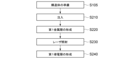
- FIG. 9 is a flowchart illustrating a method for manufacturing a semiconductor device according to the second embodiment.
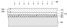
- 10A to 10C are schematic cross-sectional views illustrating the method for manufacturing the semiconductor device according to the second embodiment.
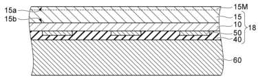
- 11A to 11C are schematic cross-sectional views illustrating the method for manufacturing the semiconductor device according to the second embodiment.
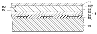
- 12A to 12C are schematic cross-sectional views illustrating the method for manufacturing the semiconductor device according to the second embodiment.
- 13A to 13C are schematic cross-sectional views illustrating the method for manufacturing the semiconductor device according to the second embodiment.
- 14A to 14C are schematic cross-sectional views illustrating the method for manufacturing the semiconductor device according to the second embodiment.
- FIG. 15 is a schematic cross-sectional view illustrating a semiconductor device according to the third embodiment.
- FIG. 1 is a flowchart illustrating a method for manufacturing a semiconductor device according to the first embodiment.
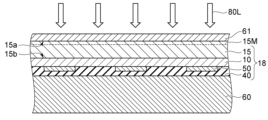
- 2 to 8 are schematic cross-sectional views illustrating the method for manufacturing the semiconductor device according to the first embodiment. 1 and 2, for example, a structure 18 is prepared (step S105).
- the structure 18 includes a substrate 15.
- the substrate 15 may be, for example, a semiconductor substrate.
- the substrate 15 includes SiC.
- the substrate 15 includes a first surface 15a.
- the substrate 15 may be, for example, at least a portion of a SiC wafer.
- a first metal layer 61 is formed on the first surface 15a of the structure 18 (step S110).
- the first metal layer 61 includes a first metal element.
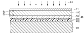
- a first element 81 is implanted into the first surface 15a through the first metal layer 61 (step S120).
- the first element 81 includes, for example, at least one selected from the group consisting of He, Ne, Ar, Kr, Xe, Rn, Si, N, P, As, B, Al, and Ga.
- the first element 81 may include, for example, at least one selected from the group consisting of He, Ne, Ar, Kr, Xe, Rn, and Si.
- the implantation is, for example, ion implantation. For example, ions of the first element 81 are implanted.
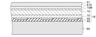
- a laser 80L is irradiated onto the first surface 15a through the first metal layer 61 (step S130). For example, laser annealing is performed. As a result, a silicide layer 61S is formed from at least a portion of the first metal layer 61, as shown in FIG. 6.
- the first element 81 is injected through the first metal layer 61. This allows a stable low-resistance ohmic contact to be obtained. This is believed to be because the injection of the first element 81 introduces a portion of the first metal element contained in the first metal layer 61 into the substrate 15. For example, it is believed that a knock-on phenomenon occurs.
- the first metal element is introduced relatively uniformly and stably near the first surface 15a of the substrate 15.
- a mixed layer (mixed region 15M described later) having a high reaction rate of the silicide reaction is uniformly formed.
- the highly reactive mixed layer is efficiently silicided by subsequent annealing using laser irradiation.
- a uniform silicide layer 61S is stably formed.
- Low electrical resistance is obtained.
- High flatness is obtained.
- high flatness and low electrical resistance are obtained.
- a manufacturing method for a semiconductor device capable of improving characteristics is provided.
- a highly flat silicide layer 61S is obtained.
- the surface morphology can be improved.
- a stable silicide layer 61S can be obtained even by low-power laser irradiation.
- a laser 80L with a low energy density can be applied.
- the efficiency of the laser irradiation process can be improved.
- a high throughput can be obtained.
- energy consumption can be reduced.
- the substrate 15 may include a second surface 15b.
- the structure 18 may include a semiconductor layer 10.
- the structure 18 may include a conductive layer 50 and an insulating member 40.
- the semiconductor layer 10 is provided between the substrate 15 and the insulating member 40.
- the conductive layer 50 is provided between the semiconductor layer 10 and the insulating member 40.
- the conductive layer 50 may be, for example, an electrode layer.
- the insulating member 40 is, for example, a passivation layer.
- the second surface 15b is between the semiconductor layer 10 and the first surface 15a.
- the first surface 15a corresponds to, for example, a surface on which an ohmic electrode is provided.
- the semiconductor layer 10 includes SiC.
- the semiconductor layer 10 may be epitaxially grown on a base (SiC wafer) that will become the substrate 15.
- a conductive layer 50 and an insulating member 40 are formed on the semiconductor layer 10.
- the base may be thinned. For example, a process such as grinding may be performed.
- preparation of the structure 18 may include thinning the thickness of the base that will become the substrate 15.
- the structure 18 when injecting the first element 81, the structure 18 may be fixed to a support member 60. This increases the mechanical strength and allows for stable processing.
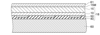
- a mixed region 15M is formed by the injection of the first element 81.
- the mixed region 15M includes, for example, Si, C, and a first metal element.
- the injection of the first element 81 may include moving a portion of the first metal element to a region including the first surface 15a of the substrate 15.
- the injection of the first element 81 forms the mixed region 15M in the region including the first surface 15a of the substrate 15.
- the formation of the mixed region 15M is due to the knock-on phenomenon, as described above.
- the first metal element includes at least one selected from the group consisting of, for example, Ti, Co, Ni, Mo, Ta, W, and Pt.
- a mixed region 15M is formed that includes such a first metal element, Si, and carbon.
- the first metal element is uniformly introduced near the first surface 15a.
- the mixed region 15M may further include a first element 81. Ti, Co, Ni, Mo, Ta, W, and Pt can react with Si to form a silicide.
- the first metal layer 61 and the mixed region 15M are irradiated with a laser 80L.
- the irradiation includes forming the silicide layer 61S from the first metal layer 61.
- the mixed region 15M may remain. At least a portion of the mixed region 15M may be amorphous. At least a portion of the mixed region 15M may include crystals (including polycrystals).
- the thickness of the first metal layer 61 is preferably 10 nm or more and 100 nm or less. If the thickness of the first metal layer 61 is excessively thin, for example, it becomes difficult to obtain a uniform silicide layer 61S. If the thickness of the first metal layer 61 is excessively thick, for example, the energy becomes excessively large during the injection of the first element 81 and/or the laser irradiation.
- the first element 81 may include at least one selected from the group consisting of Ar, B, P, and As. This makes it easier to form a mixed region 15M of an appropriate thickness. This has good compatibility with other processes. For example, an ion implantation device used to impart electrical conductivity may be used.
- the injection of the first element 81 may include the injection of a first metal element.
- the first element 81 may contain Si.
- a Si-rich mixed region 15M is obtained.
- silicon can be easily introduced into the first metal layer 61. This allows a uniform silicide layer 61S to be efficiently formed.
- a portion of silicon is introduced into the first metal layer 61. This forms a region in which the substrate 15, the region formed by knock-on, and the region where silicon is implanted into the first metal layer 61 are continuous.
- a first conductive layer 51 may be formed on the silicide layer 61S (step S140).
- the first conductive layer 51 functions as an electrode, for example.
- the first conductive layer 51 may include a metal such as aluminum, copper, or gold.
- the first conductive layer 51 is in ohmic contact with the substrate 15 with low resistance via the silicide layer 61S.
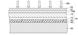
- a second metal layer 62 (see FIG. 8) may be formed (step S125). As shown in FIG. 8, the second metal layer 62 is formed on the first metal layer 61.
- the second metal layer 62 includes a second metal element.
- the second metal element may include at least one selected from the group consisting of, for example, Ti, Co, Ni, Mo, Ta, W, and Pt. The second metal element may be the same as or different from the first metal element.
- a thin first metal layer 61 is formed, and the first element 81 is injected. This efficiently forms the desired mixed region 15M. Then, the second metal layer 62 is formed. By irradiating the laser, the silicide layer 61S can be efficiently formed from the first metal layer 61 and the second metal layer 62. The silicide layer 61S of the desired thickness can be stably formed.
- the second metal element may be the same as the first metal element.
- the second metal element may be different from the first metal element.
- the structure 18 may further include a semiconductor layer 10 containing SiC.
- the semiconductor layer 10 is an epitaxially grown layer.
- laser irradiation is performed to form the silicide layer 61S. This allows the target region (the region including the first metal layer 61 and the mixed region 15M) to be locally and effectively heated. Damage to the surface device structure (semiconductor layer 10 and conductive layer 50) is suppressed.
- the temperature of the surface device structure (semiconductor layer 10 and conductive layer 50) that is increased by the laser irradiation is, for example, 50°C or higher and 1000°C or lower. The temperature may be, for example, 100°C or lower.
- the power of the laser 80L is, for example, not less than 1.0 J/cm 2 and not more than 3.0 J/cm 2. A good ohmic contact can be obtained while suppressing damage to the surface device structure (the semiconductor layer 10 and the conductive layer 50).
- FIG. 9 is a flowchart illustrating a method for manufacturing a semiconductor device according to the second embodiment.
- 10 to 14 are schematic cross-sectional views illustrating the method for manufacturing the semiconductor device according to the second embodiment. 9, in the second embodiment, after the implantation (step S210), the formation of the first metal layer 61 (step S220) is performed. Then, the irradiation of the laser 80L (step S230) is performed. Except for the order of the steps, the configuration described in relation to the first embodiment may be applied to the second embodiment.
- a structure 18 is prepared (step S105).
- the structure 18 includes a substrate 15.
- the substrate 15 includes SiC.
- the substrate 15 includes a first surface 15a.
- a metal element 85 for injection is injected into the first surface 15a of the structure 18 (step S210).
- the metal element 85 for injection includes at least one element selected from the group consisting of, for example, Ti, Co, Ni, Mo, Ta, W, and Pt.
- a mixed region 15M is formed near the first surface 15a.
- the mixed region 15M is a region that includes the first surface 15a.
- the mixed region 15M includes Si, C, and the metal element 85 to be injected.
- a first metal layer 61 containing a first metal element is formed on the first surface 15a (step S220).
- a laser 80L is irradiated onto the first surface 15a through the first metal layer 61 (step S230).
- the mixed region 15M is formed by injecting the metal element 85 before the formation of the first metal layer 61.
- the mixed region 15M can be efficiently formed by injecting the metal element 85 with low energy.
- the silicide layer 61S can be efficiently formed by irradiating the mixed region 15M containing the metal element 85 and the first metal layer 61 containing the first metal element with the laser 80L. At least a portion of the silicide layer 61S may be formed from at least a portion of the first metal layer 61. A portion of the silicide layer 61S may be formed from at least a portion of the mixed region 15M.
- the irradiation of the laser 80L (step S230) may include forming at least a portion of the silicide layer 61S from the first metal layer 61.
- a first reference example can be considered in which the first metal layer 61 is formed after injecting Ar ions or the like, and then laser irradiation is performed.
- an amorphous region is formed by injecting Ar ions or the like. This makes it possible to form silicide with a low-power laser 80L.
- a mixed region 15M is not formed.
- metal elements are supplied only from the first metal layer 61 formed on the surface. The reaction region is limited to the vicinity of the first metal layer 61. As a result, for example, there is a limit to the reduction in electrical resistance.
- the mixed region 15M is formed by injecting the metal element 85. Thereafter, the first metal layer 61 is formed, and then the laser 80L is irradiated. The laser 80L is irradiated to the mixed region 15M and the first metal layer 61, and the silicide layer 61S is formed.
- the mixed region 15M functions as, for example, a transition region.
- stress and the like are alleviated.
- the silicide layer 61S can be formed efficiently while maintaining good film quality. For example, good morphology is obtained. For example, a surface with good flatness is obtained.
- a first conductive layer 51 may be formed on the silicide layer 61S.
- the first metal element also includes at least one selected from the group consisting of Ti, Co, Ni, Mo, Ta, W, and Pt.
- the thickness of the first metal layer 61 may be 10 nm or more and 500 nm or less.
- the structure 18 may further include a semiconductor layer 10 including SiC.
- the structure 18 may include a conductive layer 50 and an insulating member 40.
- the structure 18 may be separated from the support member 60. This results in a semiconductor device.
- FIG. 15 is a schematic cross-sectional view illustrating a semiconductor device according to the third embodiment.
- the semiconductor device 110 includes a first conductive layer 51, a semiconductor layer 10, a substrate 15, a silicide layer 61S, and a mixed region 15M.
- the semiconductor layer 10 includes SiC.
- the substrate 15 includes SiC.
- the substrate 15 is provided between the first conductive layer 51 and the semiconductor layer 10.
- the silicide layer 61S is provided between the first conductive layer 51 and the substrate 15.
- the silicide layer 61S includes a first metal element and silicon.
- the mixed region 15M is provided between the silicide layer 61S and the substrate 15.
- the mixed region 15M includes a first metal element, silicon, and carbon.
- the first metal element includes at least one selected from the group consisting of Ti, Co, Ni, Mo, Ta, W, and Pt. Good ohmic contact is obtained between the first conductive layer 51 and the substrate 15. Low electrical resistance is obtained. For example, low on-resistance is obtained.
- the semiconductor device 110 includes a second conductive layer 52 and a third conductive layer 53.
- the semiconductor layer 10 includes a first semiconductor region 11, a second semiconductor region 12, a third semiconductor region 13, and a fourth semiconductor region 14.
- a first direction D1 from the first conductive layer 51 to the second conductive layer 52 is defined as the Z-axis direction.
- a direction perpendicular to the Z-axis direction is defined as the X-axis direction.
- a direction perpendicular to the Z-axis direction and the X-axis direction is defined as the Y-axis direction.
- the first semiconductor region 11 is of a first conductivity type (e.g., n-type).
- the first semiconductor region 11 includes a first partial region 11a, a second partial region 11b, and a third partial region 11c.
- a second direction D2 from the first partial region 11a to the second partial region 11b intersects with the first direction D1.
- the second direction D2 may be the X-axis direction.
- the third partial region 11c is provided between the first partial region 11a and the third conductive layer 53 in the first direction D1.
- the second semiconductor region 12 is of the second conductivity type (e.g., p-type).
- the third semiconductor region 13 is of the first conductivity type.
- the fourth semiconductor region 14 is of the second conductivity type.
- the impurity concentration of the first conductivity type in the third semiconductor region 13 is higher than the impurity concentration of the first conductivity type in the first semiconductor region 11.
- the impurity concentration of the second conductivity type in the fourth semiconductor region 14 is higher than the impurity concentration of the second conductivity type in the second semiconductor region 12.
- a part 12p of the second semiconductor region 12 is between the second partial region 11b and the third semiconductor region 13 in the first direction D1.
- the other part 12q of the second semiconductor region 12 is between the third partial region 11c and the fourth semiconductor region 14 in the second direction D2.
- the third semiconductor region 13 is between the other part 12q of the second semiconductor region 12 and the fourth semiconductor region 14 in the second direction D2.
- the second conductive layer 52 is electrically connected to the third semiconductor region 13 and the fourth semiconductor region 14.
- the insulating member 40 may include a first insulating region 41 and a second insulating region 42. At least a portion of the first insulating region 41 is provided between the third partial region 11c and the third conductive layer 53.
- the second conductive layer 52 is provided between the semiconductor layer 10 and the second insulating region 42.
- the third conductive layer 53 may extend along a third direction D3 that intersects with a plane including the first direction D1 and the second direction D2.
- the third direction D3 may be, for example, the Y-axis direction.
- the current flowing between the first conductive layer 51 and the second conductive layer 52 can be controlled by the potential of the third conductive layer 53.
- the semiconductor device 110 is, for example, a transistor.
- the first conductive layer 51 may be, for example, a drain electrode.
- the second conductive layer 52 may be, for example, a source electrode.
- the third conductive layer 53 may be, for example, a gate electrode.
- the semiconductor device 110 according to the embodiment may be, for example, a diode.
- the first conductive layer 51 may be any electrode layer.
- good ohmic contact is obtained.
- a semiconductor device with improved characteristics can be provided. For example, low electrical resistance is obtained. For example, high flatness is obtained. For example, high flatness and low electrical resistance are obtained.
- the substrate 15 may include at least one selected from the group consisting of 4H-SiC, 6H-SiC, and 3C-SiC.
- the first conductivity type impurity includes at least one selected from the group consisting of N, P, and As.
- the second conductivity type impurity includes at least one selected from the group consisting of B, Al, and Ga.
- information regarding length and thickness can be obtained by, for example, electron microscopy.
- Information regarding the composition of the material can be obtained by, for example, SIMS (Secondary Ion Mass Spectrometry) or EDX (Energy dispersive X-ray spectroscopy).
- the embodiments may include the following technical solutions.
- (Technical proposal 1) forming a first metal layer including a first metal element on a first surface of a structure including a substrate including SiC and including a first surface; Injecting a first element including at least one selected from the group consisting of He, Ne, Ar, Kr, Xe, Rn, Si, N, P, As, B, Al, and Ga into the first surface through the first metal layer; After the implantation, the first surface is irradiated with a laser through the first metal layer.
- the structure further comprises a semiconductor layer comprising SiC; the substrate further comprises a second surface; A method for manufacturing a semiconductor device described in any one of Technical Solutions 1 to 11, wherein the second surface is between the first surface and the semiconductor layer.
- the implantation includes forming an intermixed region in a portion of the substrate; the mixed region includes the first surface, The method for manufacturing a semiconductor device described in Technical Proposal 14, wherein the mixed region contains Si, C, and the metal element for injection.
- a semiconductor device comprising:
- a method for manufacturing a semiconductor device that can improve characteristics can be provided.
- 10 semiconductor layer, 11-14: first to fourth semiconductor regions, 11a-11c: first to third partial regions, 12p: part, 12q: other part, 15: substrate, 15M: mixed region, 15a, 15b: first and second surfaces, 18: structure, 40: insulating member, 41, 42: first and second insulating regions, 50: conductive layer, 51-53: first to third conductive layers, 60: support member, 61, 62: first and second metal layers, 61S: silicide layer, 80L: laser, 81: first element, 85: metal element, 110: semiconductor device, D1-D3: first to third directions
Landscapes
- Electrodes Of Semiconductors (AREA)
Abstract
特性を向上できる半導体装置の製造方法を提供する。実施形態によれば、半導体装置の製造方法は、SiCを含み第1面を含む基板を含む構造体の、前記第1面に第1金属元素を含む第1金属層を形成することを含む。前記製造方法は、前記第1金属層を介して前記第1面に、He、Ne、Ar、Kr、Xe、Rn及びSiよりなる群から選択された少なくとも1つを含む第1元素を注入することを含む。前記製造方法は、前記注入の後に、前記第1金属層を介して前記第1面にレーザを照射することを含む。
Description
本発明の実施形態は、半導体装置の製造方法に関する。
半導体装置において、特性の向上が望まれる。
実施形態は、特性を向上できる半導体装置の製造方法を提供する。
実施形態によれば、半導体装置の製造方法は、SiCを含み第1面を含む基板を含む構造体の、前記第1面に第1金属元素を含む第1金属層を形成することを含む。前記製造方法は、前記第1金属層を介して前記第1面に、He、Ne、Ar、Kr、Xe、Rn、Si、N、P、As、B、Al及びGaよりなる群から選択された少なくとも1つを含む第1元素を注入することを含む。前記製造方法は、前記注入の後に、前記第1金属層を介して前記第1面にレーザを照射することを含む。
以下に、本発明の各実施の形態について図面を参照しつつ説明する。
図面は模式的または概念的なものであり、各部分の厚さと幅との関係、部分間の大きさの比率などは、必ずしも現実のものと同一とは限らない。同じ部分を表す場合であっても、図面により互いの寸法や比率が異なって表される場合もある。
本願明細書と各図において、既出の図に関して前述したものと同様の要素には同一の符号を付して詳細な説明は適宜省略する。
図面は模式的または概念的なものであり、各部分の厚さと幅との関係、部分間の大きさの比率などは、必ずしも現実のものと同一とは限らない。同じ部分を表す場合であっても、図面により互いの寸法や比率が異なって表される場合もある。
本願明細書と各図において、既出の図に関して前述したものと同様の要素には同一の符号を付して詳細な説明は適宜省略する。
(第1実施形態)
図1は、第1実施形態に係る半導体装置の製造方法を例示するフローチャートである。
図2~図8は、第1実施形態に係る半導体装置の製造方法を例示する模式的断面図である。
図1及び図2に示すように、例えば、構造体18が準備される(ステップS105)。図2に示すように、構造体18は、基板15を含む。基板15は、例えば、半導体基板で良い。基板15は、SiCを含む。基板15は、第1面15aを含む。基板15は、例えば、SiCウエーハの少なくとも一部でよい。
図1は、第1実施形態に係る半導体装置の製造方法を例示するフローチャートである。
図2~図8は、第1実施形態に係る半導体装置の製造方法を例示する模式的断面図である。
図1及び図2に示すように、例えば、構造体18が準備される(ステップS105)。図2に示すように、構造体18は、基板15を含む。基板15は、例えば、半導体基板で良い。基板15は、SiCを含む。基板15は、第1面15aを含む。基板15は、例えば、SiCウエーハの少なくとも一部でよい。
図1及び図2に示すように、構造体18の、第1面15aに、第1金属層61を形成する(ステップS110)。第1金属層61は、第1金属元素を含む。
図1及び図3に示すように、第1金属層61を介して、第1面15aに、第1元素81を注入する(ステップS120)。第1元素81は、例えば、He、Ne、Ar、Kr、Xe、Rn、Si、N、P、As、B、Al及びGaよりなる群から選択された少なくとも1つを含む。第1元素81は、例えば、He、Ne、Ar、Kr、Xe、Rn及びSiよりなる群から選択された少なくとも1つを含んで良い。注入は、例えば、イオン注入である。例えば、第1元素81のイオンが注入される。
図1及び図5に示すように、注入の後に、第1金属層61を介して第1面15aにレーザ80Lを照射する(ステップS130)。例えば、レーザアニールが行われる。これにより、図6に示すように、第1金属層61の少なくとも一部からシリサイド層61Sが形成される。
実施形態においては、第1金属層61が形成された後に、第1金属層61を介して第1元素81の注入が行われる。これにより、低抵抗のオーミック接触が安定して得られる。これは、第1元素81の注入により、第1金属層61に含まれる第1金属元素の一部が基板15に導入されることが原因であると考えられる。例えば、ノックオン現象が生じると考えられる。
例えば、基板15の第1面15aの近傍に第1金属元素が比較的均一に安定して導入される。これにより、シリサイド反応の反応速度が高い混合層(後述する混合領域15M)が均一に形成される。その後のレーザ照射によるアニールで、反応性が高い混合層が効率よくシリサイド化される。これにより、均一なシリサイド層61Sが安定して形成される。これにより、低い電気抵抗が得られる。高い平坦性が得られる。例えば、高い平坦性と、低い電気抵抗と、が得られる。実施形態によれば、特性を向上できる半導体装置の製造方法が提供される。例えば、高い平坦性のシリサイド層61Sが得られる。表面モフォロジーが改善できる。
実施形態においては、第1金属層61を介した第1元素81の注入の後に、レーザアニールが行われる。これにより、低パワーのレーザ照射によっても、安定したシリサイド層61Sが得られる。例えば、低エネルギー密度のレーザ80Lが適用可能となる。これにより、レーザ照射工程が効率化できる。例えば、高いスループットが得られる。例えば、エネルギー消費量を低減できる。
図2に示すように、基板15は、第2面15bを含んで良い。構造体18は、基板15に加えて、半導体層10を含んで良い。構造体18は、導電層50及び絶縁部材40を含んで良い。
例えば、基板15と絶縁部材40との間に半導体層10が設けられる。半導体層10と絶縁部材40との間に導電層50が設けられる。導電層50は、例えば、電極層で良い。絶縁部材40は、例えば、パッシべーション層などである。第2面15bは、半導体層10と第1面15aとの間にある。第1面15aは、例えば、オーミック電極が設けられる面に対応する。例えば、半導体層10は、SiCを含む。
例えば、基板15となる基体(SiCウエーハ)の上に例えば、半導体層10の少なくとも一部がエピタキシャル成長されて良い。半導体層10に導電層50及び絶縁部材40が形成される。この後、上記の基体が薄くされて良い。例えば、研削などの処理が実施されて良い。このように、構造体18の準備(ステップS105)は、基板15となる基体の厚さを薄くすることを含んで良い。
図2及び図3に示すように、第1元素81の注入において、構造体18は、支持部材60に固定されて良い。機械的な強度が上昇し、安定した処理が実施できる。
図3及び図4に示すように、第1元素81の注入により、混合領域15Mが形成される。混合領域15Mは、例えば、Si、C及び第1金属元素を含む。例えば、第1元素81の注入は、基板15の第1面15aを含む領域に、第1金属元素の一部を移動させることを含んで良い。例えば、第1元素81の注入により、基板15の第1面15aを含む領域に、混合領域15Mが形成される。混合領域15Mの形成は、上記のように、ノックオン現象に起因する。
第1金属元素は、例えば、Ti、Co、Ni、Mo、Ta、W、及び、Ptよりなる群から選択された少なくとも1つを含む。このような第1金属元素と、Siと、炭素と、を含む混合領域15Mが形成される。例えば、第1金属元素は、第1面15aの近傍に、均一に導入される。混合領域15Mは、第1元素81をさらに含んで良い。Ti、Co、Ni、Mo、Ta、W、及び、Ptは、Siと反応して、シリサイドを形成することが可能である。
図5に示すように、第1金属層61及び混合領域15Mにレーザ80Lが照射される。これにより、図6に示すように、シリサイド層61Sが形成される。このように、照射は、第1金属層61からシリサイド層61Sを形成することを含む。シリサイド層61Sが形成された後に、混合領域15Mは残って良い。混合領域15Mの少なくとも一部は、アモルファスでも良い。混合領域15Mの少なくとも一部は、結晶(多結晶を含む)を含んで良い。
実施形態において、第1金属層61の厚さは、10nm以上100nm以下であることが好ましい。第1金属層61の厚さが過度に薄いと、例えば、均一なシリサイド層61Sが得難くなる。第1金属層61の厚さが過度に厚いと、例えば、第1元素81の注入、及び/または、レーザ照射において、エネルギーが過度に大きくなる。
実施形態において、第1元素81は、Ar、B、P、及びAsよりなる群から選択された少なくとも1つを含んで良い。これにより、適度な厚さの混合領域15Mを形成し易くなる。他の工程との整合性が良好である。例えば、導電性の付与のために用いられるイオン注入装置が使用されて良い。
第1元素81の注入は、第1金属元素の注入を含んでも良い。
実施形態において、第1元素81は、Siを含んで良い。例えば、Siリッチな混合領域15Mが得られる。例えば、第1金属層61中にシリコンを導入することが容易になる。これにより、均一なシリサイド層61Sを効率的に形成できる。例えば、第1金属層61中にシリコンの一部が導入される。これにより、基板15と、ノックオンにより形成された領域と、第1金属層61にシリコンが注入された領域と、が連続する領域が形成される。
図1及び図7に示すように、レーザ80Lの照射の後に、シリサイド層61Sの上に第1導電層51を形成して良い(ステップS140)。第1導電層51は、例えば、電極として機能する。第1導電層51は、例えば、アルミニウム、銅または金などの金属を含んで良い。第1導電層51は、基板15と、シリサイド層61Sを介して、低い抵抗で、オーミック接触する。
図1に示すように、注入(ステップS120)と、照射(ステップS130)と、の間において、第2金属層62(図8参照)を形成しても良い(ステップS125)。図8に示すように、第2金属層62は、第1金属層61の上に形成される。第2金属層62は、第2金属元素を含む。第2金属元素は、例えば、Ti、Co、Ni、Mo、Ta、W及びPtよりなる群から選択された少なくとも1つを含んで良い。第2金属元素は、第1金属元素と同じでも、異なっても良い。
例えば、薄い第1金属層61を形成し、第1元素81の注入が行われる。これにより、目的とする混合領域15Mが効率的に形成される。その後に、第2金属層62が形成される。レーザ照射により、第1金属層61及び第2金属層62からシリサイド層61Sが効率よく形成できる。目的とする厚さのシリサイド層61Sが安定して形成できる。
第2金属元素が第1金属元素と同じで良い。第2金属元素は第1金属元素と異なっても良い。
既に説明したように、構造体18は、SiCを含む半導体層10をさらに含んで良い。半導体層10が設けられることで、より高い品質が得られる。半導体層10は、エピタキシャル成長層である。実施形態においては、シリサイド層61Sの形成のためにレーザ照射が行われる。これにより、目的とする領域(第1金属層61及び混合領域15Mを含む領域)を局所的に効果的に加熱できる。表面デバイス構造(半導体層10及び導電層50)へのダメージが抑制される。レーザ照射によって上昇する表面デバイス構造(半導体層10及び導電層50)の温度は、例えば、50℃以上1000℃以下である。温度は、例えば、100℃以下で良い。
実施形態において、レーザ80Lのパワーは、例えば、1.0J/cm2以上3.0J/cm2以下である。表面デバイス構造(半導体層10及び導電層50)へのダメージを抑制しつつ、良好なオーミック接触が得られる。
(第2実施形態)
図9は、第2実施形態に係る半導体装置の製造方法を例示するフローチャートである。
図10~図14は、第2実施形態に係る半導体装置の製造方法を例示する模式的断面図である。
図9に示すように、第2実施形態においては、注入(ステップS210)の後に、第1金属層61の形成(ステップS220)が実施される。その後、レーザ80Lの照射(ステップS230)が実施される。このような工程の順番を除いて、第2実施形態には、第1実施形態に関して説明した構成が適用されて良い。
図9は、第2実施形態に係る半導体装置の製造方法を例示するフローチャートである。
図10~図14は、第2実施形態に係る半導体装置の製造方法を例示する模式的断面図である。
図9に示すように、第2実施形態においては、注入(ステップS210)の後に、第1金属層61の形成(ステップS220)が実施される。その後、レーザ80Lの照射(ステップS230)が実施される。このような工程の順番を除いて、第2実施形態には、第1実施形態に関して説明した構成が適用されて良い。
例えば、図10に示すように、例えば、構造体18が準備される(ステップS105)。図10に示すように、構造体18は、基板15を含む。基板15は、SiCを含む。基板15は、第1面15aを含む。
図10に示すように、構造体18の第1面15aに注入用の金属元素85を注入する(ステップS210)。注入用の金属元素85は、例えば、Ti、Co、Ni、Mo、Ta、W、及び,Ptよりなる群から選択された少なくとも1つを含む。
図11に示すように、金属元素85が注入されることで、第1面15aの近傍に、混合領域15Mが形成される。混合領域15Mは、第1面15aを含む領域である。混合領域15Mは、Si、C、及び、注入用の金属元素85を含む。
図12に示すように、注入の後に、第1面15aに第1金属元素を含む第1金属層61を形成する(ステップS220)。図13に示すように、第1金属層61を介して、第1面15aにレーザ80Lを照射する(ステップS230)。
第2実施形態においては、第1金属層61の形成の前に、金属元素85を注入することで、混合領域15Mが形成される。低いエネルギーの金属元素85の注入により、混合領域15Mが効率的に形成できる。金属元素85を含む混合領域15M、及び、第1金属元素を含む第1金属層61にレーザ80Lが照射されることで、シリサイド層61Sが効率的に形成できる。シリサイド層61Sの少なくとも一部は、第1金属層61の少なくとも一部から形成されて良い。シリサイド層61Sの一部は、混合領域15Mの少なくとも一部から形成されて良い。このように、レーザ80Lの照射(ステップS230)は、第1金属層61からシリサイド層61Sの少なくとも一部を形成することを含んで良い。
例えば、Arイオンなどを注入した後に第1金属層61を形成し、その後レーザ照射する第1参考例が考えられる。第1参考例においては、Arイオンなどの注入によりアモルファス領域が形成される。これにより、低パワーのレーザ80Lによりシリサイドを形成できる可能がある。しかしながら、第1参考例においては、混合領域15Mが形成されない。第1参考例においては、シリサイド反応において、表面に形成された第1金属層61からのみ、金属元素が供給される。反応領域は、第1金属層61の近傍のみになる。このため、例えば、電気抵抗の低減に限界がある。
これに対して、実施形態においては、金属元素85の注入により混合領域15Mが形成される。その後、第1金属層61が形成され、さらにレーザ80Lが照射される。レーザ80Lは、混合領域15M及び第1金属層61に照射され、シリサイド層61Sが形成される。混合領域15Mは、例えば、遷移領域として機能する。シリサイド層61Sの形成時に、応力などが緩和される。例えば、良好な膜質を維持しつつ、シリサイド層61Sを効率的に形成できる。例えば、良好なモフォロジーが得られる。例えば、良好な平坦性の表面が得られる。
図9及び図14に示すように、レーザ80Lの照射(ステップS230)の後に、シリサイド層61Sの上に第1導電層51を形成しても良い。
第2実施形態においても、第1金属元素は、Ti、Co、Ni、Mo、Ta、W、及び、Ptよりなる群から選択された少なくとも1つを含む。第2実施形態において、第1金属層61の厚さは、10nm以上500nm以下で良い。第2実施形態においても、構造体18は、SiCを含む半導体層10をさらに含んでも良い。第2実施形態において、構造体18は、導電層50及び絶縁部材40を含んで良い。
第1実施形態及び第2実施形態において、レーザ照射の後、または、第1導電層51の形成の後に、構造体18は、支持部材60から分離されて良い。これにより半導体装置が得られる。
(第3実施形態)
第3実施形態は、半導体装置に係る。
図15は、第3実施形態に係る半導体装置を例示する模式的断面図である。
図15に示すように、実施形態に係る半導体装置110は、第1導電層51と、半導体層10と、基板15と、シリサイド層61Sと、混合領域15Mと、を含む。半導体層10は、SiCを含む。基板15は、SiCを含む。基板15は、第1導電層51と半導体層10との間に設けられる。シリサイド層61Sは、第1導電層51と基板15との間に設けられる。シリサイド層61Sは、第1金属元素及びシリコンを含む。混合領域15Mは、シリサイド層61Sと基板15との間に設けられる。混合領域15Mは、第1金属元素とシリコンと炭素とを含む。
第3実施形態は、半導体装置に係る。
図15は、第3実施形態に係る半導体装置を例示する模式的断面図である。
図15に示すように、実施形態に係る半導体装置110は、第1導電層51と、半導体層10と、基板15と、シリサイド層61Sと、混合領域15Mと、を含む。半導体層10は、SiCを含む。基板15は、SiCを含む。基板15は、第1導電層51と半導体層10との間に設けられる。シリサイド層61Sは、第1導電層51と基板15との間に設けられる。シリサイド層61Sは、第1金属元素及びシリコンを含む。混合領域15Mは、シリサイド層61Sと基板15との間に設けられる。混合領域15Mは、第1金属元素とシリコンと炭素とを含む。
第1金属元素は、Ti、Co、Ni、Mo、Ta、W、及び、Ptよりなる群から選択された少なくとも1つを含む。第1導電層51と基板15との間において、良好なオーミック接触が得られる。低い電気抵抗が得られる。例えば、低いオン抵抗が得られる。
図15に示すように、この例では、半導体装置110は、第2導電層52及び第3導電層53を含む。半導体層10は、第1半導体領域11、第2半導体領域12、第3半導体領域13及び第4半導体領域14を含む。第1導電層51から第2導電層52への第1方向D1をZ軸方向とする。Z軸方向に対して垂直な1つの方向をX軸方向とする。Z軸方向及びX軸方向に対して垂直な方向をY軸方向とする。
第1半導体領域11は、第1導電形(例えばn形)である。第1半導体領域11は、第1部分領域11a、第2部分領域11b、第3部分領域11cを含む。第1部分領域11aから第2部分領域11bへの第2方向D2は、第1方向D1と交差する。第2方向D2は、X軸方向で良い。第3部分領域11cは、第1方向D1において、第1部分領域11aと第3導電層53との間に設けられる。
第2半導体領域12は、第2導電形(例えばp形)である。第3半導体領域13は、第1導電形である。第4半導体領域14は、第2導電形である。第3半導体領域13における第1導電形の不純物濃度は、第1半導体領域11における第1導電形の不純物濃度よりも高い。第4半導体領域14における第2導電形の不純物濃度は、第2半導体領域12における第2導電形の不純物濃度よりも高い。
第2半導体領域12の一部12pは、第1方向D1において、第2部分領域11bと第3半導体領域13との間にある。第2半導体領域12の他部12qは、第2方向D2において、第3部分領域11cと第4半導体領域14との間にある。第3半導体領域13は、第2方向D2において、第2半導体領域12の他部12qと、第4半導体領域14と、の間にある。
第2導電層52は、第3半導体領域13及び第4半導体領域14と電気的に接続される。絶縁部材40は、第1絶縁領域41及び第2絶縁領域42を含んで良い。第1絶縁領域41の少なくとも一部は、第3部分領域11cと第3導電層53との間に設けられる。第2導電層52は、半導体層10と第2絶縁領域42との間に設けられる。第3導電層53は、第1方向D1及び第2方向D2を含む平面と交差する第3方向D3に沿って延びて良い。第3方向D3は、例えば、Y軸方向で良い。
第1導電層51と第2導電層52との間に流れる電流は、第3導電層53の電位により制御できる。半導体装置110は、例えばトランジスタである。第1導電層51は、例えば、ドレイン電極で良い。第2導電層52は、ソース電極で良い。第3導電層53は、ゲート電極で良い。
実施形態に係る半導体装置110は、例えば、ダイオードでも良い。第1導電層51は、任意の電極層で良い。実施形態に係る半導体装置110において、良好なオーミック接触が得られる。特性を向上できる半導体装置を提供できる。例えば、低い電気抵抗が得られる。例えば、高い平坦性が得られる。例えば、高い平坦性と、低い電気抵抗と、が得られる。
実施形態において、例えば、基板15は、4H-SiC、6H-SiC及び3C-SiCよりなる群から選択された少なくとも1つを含んで良い。
例えば、第1導電形の不純物は、N、P及びAsよりなる群から選択された少なくとも1つを含む。例えば、第2導電形の不純物は、B、Al及びGaよりなる群から選択された少なくとも1つを含む。
実施形態において、長さ及び厚さに関する情報は電子顕微鏡観察などにより得られる。材料の組成に関する情報は、SIMS(Secondary Ion Mass Spectrometry)またはEDX(Energy dispersive X-ray spectroscopy)などにより得られる。
実施形態は、以下の技術案を含んで良い。
(技術案1)
SiCを含み第1面を含む基板を含む構造体の、前記第1面に第1金属元素を含む第1金属層を形成し、
前記第1金属層を介して前記第1面に、He、Ne、Ar、Kr、Xe、Rn、Si、N、P、As、B、Al及びGaよりなる群から選択された少なくとも1つを含む第1元素を注入し、
前記注入の後に、前記第1金属層を介して前記第1面にレーザを照射する、半導体装置の製造方法。
(技術案1)
SiCを含み第1面を含む基板を含む構造体の、前記第1面に第1金属元素を含む第1金属層を形成し、
前記第1金属層を介して前記第1面に、He、Ne、Ar、Kr、Xe、Rn、Si、N、P、As、B、Al及びGaよりなる群から選択された少なくとも1つを含む第1元素を注入し、
前記注入の後に、前記第1金属層を介して前記第1面にレーザを照射する、半導体装置の製造方法。
(技術案2)
前記注入は、前記基板の前記第1面を含む領域に前記第1金属元素の一部を移動させることを含む、技術案1に記載の半導体装置の製造方法。
前記注入は、前記基板の前記第1面を含む領域に前記第1金属元素の一部を移動させることを含む、技術案1に記載の半導体装置の製造方法。
(技術案3)
前記注入により、前記基板の前記第1面を含む領域に混合領域が形成され、
前記混合領域は、Si、C及び前記第1金属元素を含む、技術案1に記載の半導体装置の製造方法。
前記注入により、前記基板の前記第1面を含む領域に混合領域が形成され、
前記混合領域は、Si、C及び前記第1金属元素を含む、技術案1に記載の半導体装置の製造方法。
(技術案4)
前記第1金属元素は、Ti、Co、Ni、Mo、W、Ta及びPtよりなる群から選択された少なくとも1つを含む、技術案2または3に記載の半導体装置の製造方法。
前記第1金属元素は、Ti、Co、Ni、Mo、W、Ta及びPtよりなる群から選択された少なくとも1つを含む、技術案2または3に記載の半導体装置の製造方法。
(技術案5)
前記第1元素は、Ar、B、P、及びAsよりなる群から選択された少なくとも1つを含む、技術案2~4のいずれか1つに記載の半導体装置の製造方法。
前記第1元素は、Ar、B、P、及びAsよりなる群から選択された少なくとも1つを含む、技術案2~4のいずれか1つに記載の半導体装置の製造方法。
(技術案6)
前記第1元素は、Siを含む、技術案2~4のいずれか1つに記載の半導体装置の製造方法。
前記第1元素は、Siを含む、技術案2~4のいずれか1つに記載の半導体装置の製造方法。
(技術案7)
前記照射は、前記第1金属層からシリサイド層を形成することを含む、技術案2~6のいずれか1つに記載の半導体装置の製造方法。
前記照射は、前記第1金属層からシリサイド層を形成することを含む、技術案2~6のいずれか1つに記載の半導体装置の製造方法。
(技術案8)
前記照射の後に、前記シリサイド層の上に第1導電層を形成する、技術案7に記載の半導体装置の製造方法。
前記照射の後に、前記シリサイド層の上に第1導電層を形成する、技術案7に記載の半導体装置の製造方法。
(技術案9)
前記第1金属層の厚さは、10nm以上100nm以下である、技術案1~8のいずれか1つに記載の半導体装置の製造方法。
前記第1金属層の厚さは、10nm以上100nm以下である、技術案1~8のいずれか1つに記載の半導体装置の製造方法。
(技術案10)
前記注入と前記照射との間において、前記第1金属層の上に、第2金属元素を含む第2金属層を形成する、技術案1~9のいずれか1つに記載の半導体装置の製造方法。
前記注入と前記照射との間において、前記第1金属層の上に、第2金属元素を含む第2金属層を形成する、技術案1~9のいずれか1つに記載の半導体装置の製造方法。
(技術案11)
前記第2金属元素は、前記第1金属元素と同じである、技術案10に記載の半導体装置の製造方法。
前記第2金属元素は、前記第1金属元素と同じである、技術案10に記載の半導体装置の製造方法。
(技術案12)
前記構造体は、SiCを含む半導体層をさらに含み、
前記基板は、第2面をさらに含み、
前記第2面は、前記第1面と前記半導体層との間にある、技術案1~11のいずれか1つに記載の半導体装置の製造方法。
前記構造体は、SiCを含む半導体層をさらに含み、
前記基板は、第2面をさらに含み、
前記第2面は、前記第1面と前記半導体層との間にある、技術案1~11のいずれか1つに記載の半導体装置の製造方法。
(技術案13)
前記照射によって上昇する前記半導体層の温度は、100℃以下である、技術案12に記載の半導体装置の製造方法。
前記照射によって上昇する前記半導体層の温度は、100℃以下である、技術案12に記載の半導体装置の製造方法。
(技術案14)
SiCを含み第1面を含む基板を含む構造体の、前記第1面に注入用の金属元素を注入し、
前記注入の後に、前記第1面に第1金属元素を含む第1金属層を形成し、
前記第1金属層を介して前記第1面にレーザを照射する、半導体装置の製造方法。
SiCを含み第1面を含む基板を含む構造体の、前記第1面に注入用の金属元素を注入し、
前記注入の後に、前記第1面に第1金属元素を含む第1金属層を形成し、
前記第1金属層を介して前記第1面にレーザを照射する、半導体装置の製造方法。
(技術案15)
前記注入は、前記基板の一部に混合領域を形成することを含み、
前記混合領域は、前記第1面を含み、
前記混合領域は、Si、C及び前記注入用の前記金属元素を含む、技術案14に記載の半導体装置の製造方法。
前記注入は、前記基板の一部に混合領域を形成することを含み、
前記混合領域は、前記第1面を含み、
前記混合領域は、Si、C及び前記注入用の前記金属元素を含む、技術案14に記載の半導体装置の製造方法。
(技術案16)
前記注入用の前記金属元素は、Ti、Co、Ni、Mo、Ta、W、及び、Ptよりなる群から選択された少なくとも1つを含む、技術案14または15に記載の半導体装置の製造方法。
前記注入用の前記金属元素は、Ti、Co、Ni、Mo、Ta、W、及び、Ptよりなる群から選択された少なくとも1つを含む、技術案14または15に記載の半導体装置の製造方法。
(技術案17)
前記第1金属元素は、Ti、Co、Ni、Mo、Ta、W、及び、Ptよりなる群から選択された少なくとも1つを含む、技術案14~16のいずれか1つに記載の半導体装置の製造方法。
前記第1金属元素は、Ti、Co、Ni、Mo、Ta、W、及び、Ptよりなる群から選択された少なくとも1つを含む、技術案14~16のいずれか1つに記載の半導体装置の製造方法。
(技術案18)
前記照射は、前記第1金属層からシリサイド層を形成することを含む、技術案14~17のいずれか1つに記載の半導体装置の製造方法。
前記照射は、前記第1金属層からシリサイド層を形成することを含む、技術案14~17のいずれか1つに記載の半導体装置の製造方法。
(技術案19)
前記構造体の準備をさらに備え、
前記構造体の準備は、前記基板となる基体の厚さを薄くすることを含む、技術案1~18のいずれか1つに記載の半導体装置の製造方法。
前記構造体の準備をさらに備え、
前記構造体の準備は、前記基板となる基体の厚さを薄くすることを含む、技術案1~18のいずれか1つに記載の半導体装置の製造方法。
(技術案20)
第1導電層と、
SiCを含む半導体層と、
前記第1導電層と前記半導体層との間に設けられた、SiCを含む基板と、
前記第1導電層と前記基板との間に設けられ第1金属元素及びシリコンを含むシリサイド層と、
前記シリサイド層と前記基板との間に設けられ、前記第1金属元素とシリコンと炭素とを含む混合領域と、
を備えた半導体装置。
第1導電層と、
SiCを含む半導体層と、
前記第1導電層と前記半導体層との間に設けられた、SiCを含む基板と、
前記第1導電層と前記基板との間に設けられ第1金属元素及びシリコンを含むシリサイド層と、
前記シリサイド層と前記基板との間に設けられ、前記第1金属元素とシリコンと炭素とを含む混合領域と、
を備えた半導体装置。
実施形態によれば、特性を向上できる半導体装置の製造方法が提供できる。
以上、具体例を参照しつつ、本発明の実施の形態について説明した。しかし、本発明は、これらの具体例に限定されるものではない。例えば、半導体装置または構造体に含まれる基板、半導体層及びシリサイド層などの各要素の具体的な構成に関しては、当業者が公知の範囲から適宜選択することにより本発明を同様に実施し、同様の効果を得ることができる限り、本発明の範囲に包含される。
また、各具体例のいずれか2つ以上の要素を技術的に可能な範囲で組み合わせたものも、本発明の要旨を包含する限り本発明の範囲に含まれる。
その他、本発明の実施の形態として上述した半導体装置の製造方法を基にして、当業者が適宜設計変更して実施し得る全ての半導体装置の製造方法も、本発明の要旨を包含する限り、本発明の範囲に属する。
その他、本発明の思想の範疇において、当業者であれば、各種の変更例及び修正例に想到し得るものであり、それら変更例及び修正例についても本発明の範囲に属するものと了解される。
本発明のいくつかの実施形態を説明したが、これらの実施形態は、例として提示したものであり、発明の範囲を限定することは意図していない。これら新規な実施形態は、その他の様々な形態で実施されることが可能であり、発明の要旨を逸脱しない範囲で、種々の省略、置き換え、変更を行うことができる。これら実施形態やその変形は、発明の範囲や要旨に含まれるとともに、特許請求の範囲に記載された発明とその均等の範囲に含まれる。
10:半導体層、 11~14:第1~第4半導体領域、 11a~11c:第1~第3部分領域、 12p:一部、 12q:他部、 15:基板、 15M:混合領域、 15a、15b:第1、第2面、 18:構造体、 40:絶縁部材、 41、42:第1、第2絶縁領域、 50:導電層、 51~53:第1~第3導電層、 60:支持部材、 61、62:第1、第2金属層、 61S:シリサイド層、 80L:レーザ、 81:第1元素、 85:金属元素、 110:半導体装置、 D1~D3:第1~第3方向
Claims (11)
- SiCを含み第1面を含む基板を含む構造体の、前記第1面に第1金属元素を含む第1金属層を形成し、
前記第1金属層を介して前記第1面に、He、Ne、Ar、Kr、Xe、Rn、Si、N、P、As、B、Al及びGaよりなる群から選択された少なくとも1つを含む第1元素を注入し、
前記注入の後に、前記第1金属層を介して前記第1面にレーザを照射する、半導体装置の製造方法。 - 前記注入は、前記基板の前記第1面を含む領域に前記第1金属元素の一部を移動させることを含む、請求項1に記載の半導体装置の製造方法。
- 前記注入により、前記基板の前記第1面を含む領域に混合領域が形成され、
前記混合領域は、Si、C及び前記第1金属元素を含む、請求項1に記載の半導体装置の製造方法。 - 前記第1金属元素は、Ti、Co、Ni、Mo、Ta、W、及び、Ptよりなる群から選択された少なくとも1つを含む、請求項2に記載の半導体装置の製造方法。
- 前記第1元素は、Ar、B、P、及びAsよりなる群から選択された少なくとも1つを含む、請求項2に記載の半導体装置の製造方法。
- 前記第1元素は、Siを含む、請求項2に記載の半導体装置の製造方法。
- 前記注入と前記照射との間において、前記第1金属層の上に、第2金属元素を含む第2金属層を形成する、請求項1~6のいずれか1つに記載の半導体装置の製造方法。
- SiCを含み第1面を含む基板を含む構造体の、前記第1面に注入用の金属元素を注入し、
前記注入の後に、前記第1面に第1金属元素を含む第1金属層を形成し、
前記第1金属層を介して前記第1面にレーザを照射する、半導体装置の製造方法。 - 前記注入は、前記基板の一部に混合領域を形成することを含み、
前記混合領域は、前記第1面を含み、
前記混合領域は、Si、C及び前記注入用の前記金属元素を含む、請求項8に記載の半導体装置の製造方法。 - 前記注入用の前記金属元素は、Ti、Co、Ni、Mo、Ta、W、及び、Ptよりなる群から選択された少なくとも1つを含む、請求項8に記載の半導体装置の製造方法。
- 前記第1金属元素は、Ti、Co、Ni、Mo、Ta、W、及び、Ptよりなる群から選択された少なくとも1つを含む、請求項8~10のいずれか1つに記載の半導体装置の製造方法。
Priority Applications (1)
| Application Number | Priority Date | Filing Date | Title |
|---|---|---|---|
| CN202380070983.3A CN120019477A (zh) | 2023-07-31 | 2023-11-14 | 半导体装置的制造方法 |
Applications Claiming Priority (2)
| Application Number | Priority Date | Filing Date | Title |
|---|---|---|---|
| JP2023124516A JP2025020887A (ja) | 2023-07-31 | 2023-07-31 | 半導体装置の製造方法 |
| JP2023-124516 | 2023-07-31 |
Publications (1)
| Publication Number | Publication Date |
|---|---|
| WO2025027872A1 true WO2025027872A1 (ja) | 2025-02-06 |
Family
ID=94394952
Family Applications (1)
| Application Number | Title | Priority Date | Filing Date |
|---|---|---|---|
| PCT/JP2023/040976 Pending WO2025027872A1 (ja) | 2023-07-31 | 2023-11-14 | 半導体装置の製造方法 |
Country Status (3)
| Country | Link |
|---|---|
| JP (1) | JP2025020887A (ja) |
| CN (1) | CN120019477A (ja) |
| WO (1) | WO2025027872A1 (ja) |
Citations (6)
| Publication number | Priority date | Publication date | Assignee | Title |
|---|---|---|---|---|
| JPH0982663A (ja) * | 1995-09-13 | 1997-03-28 | Fuji Electric Co Ltd | 炭化珪素半導体装置の製造方法 |
| JP2000106350A (ja) * | 1998-09-28 | 2000-04-11 | Sanyo Electric Co Ltd | オーミック電極の製造方法及び半導体素子の製造方法 |
| JP2011134809A (ja) * | 2009-12-22 | 2011-07-07 | Toyota Motor Corp | 半導体装置の製造方法 |
| JP2012004185A (ja) * | 2010-06-14 | 2012-01-05 | Denso Corp | 炭化珪素半導体装置の製造方法 |
| JP2017118104A (ja) * | 2015-12-01 | 2017-06-29 | インフィネオン テクノロジーズ アーゲーInfineon Technologies Ag | 半導体本体上の接触層形成 |
| JP2017199807A (ja) * | 2016-04-27 | 2017-11-02 | 株式会社デンソー | 炭化珪素半導体装置およびその製造方法 |
-
2023
- 2023-07-31 JP JP2023124516A patent/JP2025020887A/ja active Pending
- 2023-11-14 CN CN202380070983.3A patent/CN120019477A/zh active Pending
- 2023-11-14 WO PCT/JP2023/040976 patent/WO2025027872A1/ja active Pending
Patent Citations (6)
| Publication number | Priority date | Publication date | Assignee | Title |
|---|---|---|---|---|
| JPH0982663A (ja) * | 1995-09-13 | 1997-03-28 | Fuji Electric Co Ltd | 炭化珪素半導体装置の製造方法 |
| JP2000106350A (ja) * | 1998-09-28 | 2000-04-11 | Sanyo Electric Co Ltd | オーミック電極の製造方法及び半導体素子の製造方法 |
| JP2011134809A (ja) * | 2009-12-22 | 2011-07-07 | Toyota Motor Corp | 半導体装置の製造方法 |
| JP2012004185A (ja) * | 2010-06-14 | 2012-01-05 | Denso Corp | 炭化珪素半導体装置の製造方法 |
| JP2017118104A (ja) * | 2015-12-01 | 2017-06-29 | インフィネオン テクノロジーズ アーゲーInfineon Technologies Ag | 半導体本体上の接触層形成 |
| JP2017199807A (ja) * | 2016-04-27 | 2017-11-02 | 株式会社デンソー | 炭化珪素半導体装置およびその製造方法 |
Also Published As
| Publication number | Publication date |
|---|---|
| CN120019477A (zh) | 2025-05-16 |
| JP2025020887A (ja) | 2025-02-13 |
Similar Documents
| Publication | Publication Date | Title |
|---|---|---|
| JP3184320B2 (ja) | ダイヤモンド電界効果トランジスタ | |
| US10600921B2 (en) | Silicon carbide semiconductor device and method of manufacturing silicon carbide semiconductor device | |
| WO2010016388A1 (ja) | ショットキーバリアダイオードおよびショットキーバリアダイオードの製造方法 | |
| JP5668414B2 (ja) | 半導体装置の製造方法 | |
| US20210280424A1 (en) | Method for manufacturing a sic electronic device with reduced handling steps, and sic electronic device | |
| CN104303269A (zh) | 碳化硅半导体装置的制造方法 | |
| JP5156059B2 (ja) | ダイオードとその製造方法 | |
| CN107785251A (zh) | 使用热处理的阻挡层形成 | |
| JP6728097B2 (ja) | 半導体装置、半導体装置の製造方法、インバータ回路、駆動装置、車両、及び、昇降機 | |
| US12374545B2 (en) | Process for working a wafer of 4H—SiC material to form a 3C—SiC layer in direct contact with the 4H—SiC material | |
| JP4521327B2 (ja) | 半導体装置の製造方法 | |
| Claeys et al. | Status and trends in Ge CMOS technology | |
| WO2025027872A1 (ja) | 半導体装置の製造方法 | |
| JP6336554B2 (ja) | 半導体本体上の接触層形成 | |
| JP4087365B2 (ja) | SiC半導体装置の製造方法 | |
| JP5921089B2 (ja) | エピタキシャルウエハの製造方法及び半導体装置の製造方法 | |
| JP2000106350A (ja) | オーミック電極の製造方法及び半導体素子の製造方法 | |
| CN113178414A (zh) | 碳化硅欧姆接触结构的形成方法及mos晶体管的制备方法 | |
| US20230064469A1 (en) | Wafer, semiconductor device, method for manufacturing wafer, and method for manufacturing semiconductor device | |
| RU2594615C2 (ru) | Способ изготовления полупроводникового прибора | |
| JP2006073923A (ja) | SiC半導体装置およびSiC半導体装置の製造方法 | |
| JP5311792B2 (ja) | 半導体装置の製造方法 | |
| JP2019004033A (ja) | 半導体ウェーハの製造方法および半導体ウェーハ | |
| KR20220056164A (ko) | 반도체 소자의 콘택 및 반도체 소자의 콘택 형성 방법 | |
| US20130341646A1 (en) | Silicon carbide semiconductor device and method for manufacturing same |
Legal Events
| Date | Code | Title | Description |
|---|---|---|---|
| 121 | Ep: the epo has been informed by wipo that ep was designated in this application |
Ref document number: 23947669 Country of ref document: EP Kind code of ref document: A1 |
|
| WWE | Wipo information: entry into national phase |
Ref document number: 202380070983.3 Country of ref document: CN |
|
| WWP | Wipo information: published in national office |
Ref document number: 202380070983.3 Country of ref document: CN |
|
| NENP | Non-entry into the national phase |
Ref country code: DE |