WO2025027821A1 - 半導体装置 - Google Patents
半導体装置 Download PDFInfo
- Publication number
- WO2025027821A1 WO2025027821A1 PCT/JP2023/028245 JP2023028245W WO2025027821A1 WO 2025027821 A1 WO2025027821 A1 WO 2025027821A1 JP 2023028245 W JP2023028245 W JP 2023028245W WO 2025027821 A1 WO2025027821 A1 WO 2025027821A1
- Authority
- WO
- WIPO (PCT)
- Prior art keywords
- semiconductor device
- semiconductor
- layer
- surface bonding
- elastic modulus
- Prior art date
- Legal status (The legal status is an assumption and is not a legal conclusion. Google has not performed a legal analysis and makes no representation as to the accuracy of the status listed.)
- Pending
Links
Images



Classifications
-
- H—ELECTRICITY
- H10—SEMICONDUCTOR DEVICES; ELECTRIC SOLID-STATE DEVICES NOT OTHERWISE PROVIDED FOR
- H10W—GENERIC PACKAGES, INTERCONNECTIONS, CONNECTORS OR OTHER CONSTRUCTIONAL DETAILS OF DEVICES COVERED BY CLASS H10
- H10W72/00—Interconnections or connectors in packages
-
- H—ELECTRICITY
- H10—SEMICONDUCTOR DEVICES; ELECTRIC SOLID-STATE DEVICES NOT OTHERWISE PROVIDED FOR
- H10W—GENERIC PACKAGES, INTERCONNECTIONS, CONNECTORS OR OTHER CONSTRUCTIONAL DETAILS OF DEVICES COVERED BY CLASS H10
- H10W72/00—Interconnections or connectors in packages
- H10W72/071—Connecting or disconnecting
Definitions
- This disclosure relates to a semiconductor device.
- a semiconductor device has been proposed in which the lead frame, which is an external electrode, and the surface electrode of the semiconductor element are joined with solder (for example, Patent Document 1).
- the difference between the linear expansion coefficient of the solder or lead frame and the linear expansion coefficient of the semiconductor element causes thermal strain in the surface electrodes of the semiconductor element, and repeated thermal strain can cause cracks in the surface electrodes.
- the present disclosure has been made in consideration of the above-mentioned problems, and aims to provide a technology that can suppress thermal strain that occurs in the surface electrodes of semiconductor elements.
- the semiconductor device comprises a semiconductor layer, a surface electrode provided on the surface of the semiconductor layer, an element surface bonding layer selectively provided on the surface of the surface electrode, a lead frame located on the surface side of the element surface bonding layer, and an element surface bonding material that bonds the lead frame and the element surface bonding layer, and the elastic modulus of the element surface bonding material is 20% or less of the elastic modulus of the surface electrode.
- 1 is a cross-sectional view showing an overall configuration of a semiconductor device according to a first embodiment
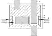
- 1 is a plan view showing an overall configuration of a semiconductor device according to a first embodiment
- 1 is an enlarged cross-sectional view showing a configuration of a portion of a semiconductor device according to a first embodiment
- 11A and 11B are diagrams showing simulation results of the semiconductor device according to the first embodiment
- FIG. 13 is a diagram showing physical property values used in a simulation.
- FIG. 1 and 2 are a cross-sectional view and a plan view, respectively, showing the overall configuration of a semiconductor device 100 according to the first embodiment, and FIG. 3 is an enlarged cross-sectional view of a dotted line portion in FIG.
- the semiconductor device includes a semiconductor element 1, an insulating material 2, an element back surface bonding material 5, a lead frame 6, an element front surface bonding material 7, signal wiring 8, a control terminal 9, and a sealing resin 10.
- the semiconductor element 1 includes, for example, any one of a MOSFET (Metal Oxide Semiconductor Field Effect Transistor), an IGBT (Insulated Gate Bipolar Transistor), an RC-IGBT (Reverse Conducting-IGBT) in which an IGBT and a diode are integrated, an SBD (Schottky Barrier Diode), and a PND (PN junction diode).
- MOSFET Metal Oxide Semiconductor Field Effect Transistor
- IGBT Insulated Gate Bipolar Transistor
- RC-IGBT Reverse Conducting-IGBT
- SBD Schottky Barrier Diode
- PND PN junction diode
- the semiconductor layer 1a includes at least one of a semiconductor wafer and an epitaxial growth layer.
- at least one of A, B, C, ..., and Z means any one of all combinations of one or more types extracted from the group of A, B, C, ..., and Z.
- the material of the semiconductor layer 1a may include Si, or may include a wide band gap semiconductor such as SiC, GaN, or diamond. When the material of the semiconductor layer 1a includes a wide band gap semiconductor, the semiconductor element 1 can operate stably under high temperatures and high voltages, and can achieve high switching speeds.
- the surface electrode 1b is provided on the surface of the semiconductor layer 1a.
- the material of the surface electrode 1b contains, for example, Al as a main component.
- the element surface bonding layer 1c is selectively provided on the surface of the surface electrode 1b.
- the material of the element surface bonding layer 1c contains, for example, Ni as a main component.
- the outermost surface of the element surface bonding layer 1c may contain a layer that has good bonding properties with the element surface bonding material 7.
- the outermost surface of the element surface bonding layer 1c may contain an Au layer that has good bonding properties with solder.
- the Young's modulus of the element surface bonding layer 1c is, for example, 150 Gpa or more and 200 Gpa or less.
- the protective film 1d is selectively provided on the surface of the surface electrode 1b and surrounds the element surface bonding layer 1c when viewed from above.
- the material of the protective film 1d includes, for example, polyimide.
- the material of the insulating material 2 includes, for example, insulating resin or ceramic.
- the insulating resin of the insulating material 2 includes, for example, epoxy resin as a main component, and the ceramic of the insulating material 2 includes, for example, at least one of Al2O3 , Si3N4 , and AlN as a main component.
- the insulating material 2 is required to have not only insulating properties but also heat dissipation properties, it is generally desirable to make the insulating material 2 thin in order to increase the thermal conductivity of the insulating material 2. However, if the insulating material 2 is made too thin, there is a possibility that the insulating capacity may be insufficient or that the structural capacity (e.g. stress resistance) during manufacturing may be insufficient, so it is desirable for the thickness of the insulating material 2 to be 100 ⁇ m or more.
- the insulating material 2 has a front surface and a back surface on which a front conductive material 3 and a back conductive material 4 are respectively provided.
- the material of the front conductive material 3 and the back conductive material 4 includes at least one metal of Al, Al alloy, Cu, and Cu alloy, for example.
- the front conductive material 3 and the back conductive material 4 are located below the semiconductor element 1 and have the function of diffusing heat from the semiconductor element 1, so it is desirable that they have a sufficient thickness to allow sufficient heat diffusion in the planar direction. Although it depends on the planar layout, it is desirable that the front conductive material 3 and the back conductive material 4 have a thickness of, for example, 0.4 mm or more.
- the element back surface bonding material 5 electrically connects the back surface of the semiconductor layer 1a to the surface conductive material 3 of the insulating material 2.
- the element back surface bonding material 5 bonds a back surface electrode (not shown) provided on the back surface of the semiconductor layer 1a to the surface conductive material 3.
- the material of the element back surface bonding material 5 may include, for example, a lead-free solder mainly composed of Sn, or may include a sintered material mainly composed of Ag or Cu.
- the element back surface bonding material 5 In order to dissipate heat from the semiconductor element 1 to the back surface side of the semiconductor device 100, it is desirable for the element back surface bonding material 5 to have a thickness of, for example, 0.15 mm or less.
- the lead frame 6 is located on the surface side of the element surface bonding layer 1c.
- the material of the lead frame 6 contains a metal with good conductivity, for example, at least one of Al, Al alloy, Cu, and Cu alloy. Since the lead frame 6 constitutes the main current path of the semiconductor device 100, it is desirable for the current cross-sectional area to be large. Although it depends on the planar layout, it is desirable for the lead frame 6 to have a thickness of, for example, 0.1 mm or more.
- the element surface bonding material 7 bonds the lead frame 6 and the element surface bonding layer 1c.
- the material of the element surface bonding material 7 includes a tin alloy and a thermoplastic resin. Details of the element surface bonding material 7 will be described later.
- the signal wiring 8 in FIG. 1 connects a signal electrode such as a gate electrode of the semiconductor element 1 to a control terminal 9.
- the signal wiring 8 is made of a wire made of, for example, Al, Cu, Ag, or the like.
- the signal wiring 8 it is desirable for the signal wiring 8 to have a diameter of 100 ⁇ m or more.
- the material of the control terminal 9 contains a metal with good conductivity, for example, at least one of Al, an Al alloy, Cu, and a Cu alloy.
- the sealing resin 10 seals at least the semiconductor layer 1a.
- the sealing resin 10 seals the semiconductor element 1, the insulating material 2, the front conductive material 3, part of the rear conductive material 4, the element rear surface bonding material 5, part of the lead frame 6, the element front surface bonding material 7, the signal wiring 8, and part of the control terminal 9.
- the material of the sealing resin 10 it depends on the linear expansion coefficients of the semiconductor element 1 and the lead frame 6, it is desirable for the material of the sealing resin 10 to be a mold resin with a linear expansion coefficient of about 10 to 18 ppm/K.
- the difference between the linear expansion coefficient of the element surface bonding material 7 or the lead frame 6 and the linear expansion coefficient of the semiconductor element 1 causes thermal deformation such as thermal expansion or thermal contraction in the element surface bonding material 7 or the lead frame 6.
- This thermal deformation is transmitted to the surface electrode 1b via the element surface bonding layer 1c, and thermal strain occurs in the surface electrode 1b.
- the Manson-Coffin law applies, which correlates the fracture life and the strain amplitude of the thermal strain, and the greater the strain amplitude of the surface electrode 1b, the shorter the fracture life of the surface electrode 1b. Therefore, the inventor investigated a configuration that reduces the strain amplitude of the thermal strain generated in the surface electrode 1b.
- Figure 4 shows the results of a simulation of strain amplitude using a two-dimensional model with the same configuration as Figure 3.
- Figure 4 shows the relationship between the change in the ratio of the elastic modulus of the element surface bonding material 7 to the elastic modulus of the surface electrode 1b (hereinafter sometimes referred to as the "elastic modulus ratio") and the strain amplitude of thermal strain generated in the surface electrode 1b.
- the elastic modulus here refers to Young's modulus that can be measured by bending tests, etc.
- the physical property values shown in Figure 5 were used as the physical property values of each component, and the Young's modulus of the element surface bonding material was used such that the elastic modulus ratios are 5%, 10%, 15%, 20%, 30%, and 50%.
- the strain amplitude of the thermal strain generated in surface electrode 1b can be reduced.
- the material of the element surface bonding material 7 contains, for example, a tin alloy and a thermoplastic resin. Therefore, by increasing the ratio of thermoplastic resin to tin alloy in the element surface bonding material 7, the elastic modulus of the element surface bonding material 7 can be made 20% or less of the elastic modulus of the surface electrode 1b.
- the elastic modulus (Young's modulus) of the surface electrode 1b is about 70 GPa, so the ratio of thermoplastic resin in the element surface bonding material 7 is adjusted so that the elastic modulus (Young's modulus) of the element surface bonding material 7 is 14 GPa or less. Also, in order to stably reduce the strain amplitude generated in the surface electrode 1b due to thermal deformation of the lead frame 6, it is desirable for the element surface bonding material 7 to have a thickness of 0.2 mm or more.
- the effect of reducing the strain amplitude of the surface electrode 1b as described above is particularly effective when the semiconductor layer 1a of the semiconductor element 1 includes a wide band gap semiconductor capable of stable operation at high temperatures.
Landscapes
- Structures Or Materials For Encapsulating Or Coating Semiconductor Devices Or Solid State Devices (AREA)
- Die Bonding (AREA)
Priority Applications (3)
| Application Number | Priority Date | Filing Date | Title |
|---|---|---|---|
| PCT/JP2023/028245 WO2025027821A1 (ja) | 2023-08-02 | 2023-08-02 | 半導体装置 |
| JP2025538138A JPWO2025027821A1 (https=) | 2023-08-02 | 2023-08-02 | |
| CN202380100836.6A CN121694062A (zh) | 2023-08-02 | 2023-08-02 | 半导体装置 |
Applications Claiming Priority (1)
| Application Number | Priority Date | Filing Date | Title |
|---|---|---|---|
| PCT/JP2023/028245 WO2025027821A1 (ja) | 2023-08-02 | 2023-08-02 | 半導体装置 |
Publications (1)
| Publication Number | Publication Date |
|---|---|
| WO2025027821A1 true WO2025027821A1 (ja) | 2025-02-06 |
Family
ID=94394884
Family Applications (1)
| Application Number | Title | Priority Date | Filing Date |
|---|---|---|---|
| PCT/JP2023/028245 Pending WO2025027821A1 (ja) | 2023-08-02 | 2023-08-02 | 半導体装置 |
Country Status (3)
| Country | Link |
|---|---|
| JP (1) | JPWO2025027821A1 (https=) |
| CN (1) | CN121694062A (https=) |
| WO (1) | WO2025027821A1 (https=) |
Citations (3)
| Publication number | Priority date | Publication date | Assignee | Title |
|---|---|---|---|---|
| JP2017084881A (ja) * | 2015-10-23 | 2017-05-18 | 富士電機株式会社 | 半導体装置 |
| WO2017103978A1 (ja) * | 2015-12-14 | 2017-06-22 | 三菱電機株式会社 | 半導体装置及びその製造方法 |
| JP2018026417A (ja) * | 2016-08-09 | 2018-02-15 | 三菱電機株式会社 | 電力用半導体装置 |
-
2023
- 2023-08-02 CN CN202380100836.6A patent/CN121694062A/zh active Pending
- 2023-08-02 JP JP2025538138A patent/JPWO2025027821A1/ja active Pending
- 2023-08-02 WO PCT/JP2023/028245 patent/WO2025027821A1/ja active Pending
Patent Citations (3)
| Publication number | Priority date | Publication date | Assignee | Title |
|---|---|---|---|---|
| JP2017084881A (ja) * | 2015-10-23 | 2017-05-18 | 富士電機株式会社 | 半導体装置 |
| WO2017103978A1 (ja) * | 2015-12-14 | 2017-06-22 | 三菱電機株式会社 | 半導体装置及びその製造方法 |
| JP2018026417A (ja) * | 2016-08-09 | 2018-02-15 | 三菱電機株式会社 | 電力用半導体装置 |
Also Published As
| Publication number | Publication date |
|---|---|
| CN121694062A (zh) | 2026-03-17 |
| JPWO2025027821A1 (https=) | 2025-02-06 |
Similar Documents
| Publication | Publication Date | Title |
|---|---|---|
| US10861833B2 (en) | Semiconductor device | |
| US10510640B2 (en) | Semiconductor device and method for manufacturing semiconductor device | |
| US8466548B2 (en) | Semiconductor device including excess solder | |
| JP7661267B2 (ja) | 半導体装置 | |
| CN114846593B (zh) | 半导体装置 | |
| JP2022038766A (ja) | 半導体モジュール | |
| JP2025142343A (ja) | 半導体装置 | |
| US6512304B2 (en) | Nickel-iron expansion contact for semiconductor die | |
| JP4171355B2 (ja) | モールド型パワーデバイス | |
| JP7495225B2 (ja) | 半導体装置 | |
| JP2015167171A (ja) | 半導体装置 | |
| JP2019009280A (ja) | 半導体装置 | |
| WO2025027821A1 (ja) | 半導体装置 | |
| US12538795B2 (en) | Semiconductor component and semiconductor device | |
| JP2015115349A (ja) | 半導体装置 | |
| JP7607438B2 (ja) | 半導体装置 | |
| US20240258188A1 (en) | Semiconductor device | |
| CN116325129A (zh) | 半导体装置 | |
| CN118235233A (zh) | 半导体装置以及半导体装置的制造方法 | |
| TW201608692A (zh) | 半導體晶片及電子組件 | |
| JP7570298B2 (ja) | 半導体装置 | |
| US11823985B2 (en) | Leadframe, semiconductor device, and method for manufacturing semiconductor device | |
| JP2021044456A (ja) | 半導体装置 | |
| US20220115347A1 (en) | Semiconductor device and method for manufacturing the same | |
| US11114387B2 (en) | Electronic packaging structure |
Legal Events
| Date | Code | Title | Description |
|---|---|---|---|
| 121 | Ep: the epo has been informed by wipo that ep was designated in this application |
Ref document number: 23947618 Country of ref document: EP Kind code of ref document: A1 |
|
| ENP | Entry into the national phase |
Ref document number: 2025538138 Country of ref document: JP Kind code of ref document: A |
|
| WWE | Wipo information: entry into national phase |
Ref document number: 2025538138 Country of ref document: JP |