WO2025022969A1 - 半導体装置の製造方法、半導体装置および車両 - Google Patents
半導体装置の製造方法、半導体装置および車両 Download PDFInfo
- Publication number
- WO2025022969A1 WO2025022969A1 PCT/JP2024/024181 JP2024024181W WO2025022969A1 WO 2025022969 A1 WO2025022969 A1 WO 2025022969A1 JP 2024024181 W JP2024024181 W JP 2024024181W WO 2025022969 A1 WO2025022969 A1 WO 2025022969A1
- Authority
- WO
- WIPO (PCT)
- Prior art keywords
- semiconductor device
- sealing resin
- layer
- manufacturing
- heat dissipation
- Prior art date
- Legal status (The legal status is an assumption and is not a legal conclusion. Google has not performed a legal analysis and makes no representation as to the accuracy of the status listed.)
- Pending
Links
Images




















Classifications
-
- H—ELECTRICITY
- H10—SEMICONDUCTOR DEVICES; ELECTRIC SOLID-STATE DEVICES NOT OTHERWISE PROVIDED FOR
- H10W—GENERIC PACKAGES, INTERCONNECTIONS, CONNECTORS OR OTHER CONSTRUCTIONAL DETAILS OF DEVICES COVERED BY CLASS H10
- H10W40/00—Arrangements for thermal protection or thermal control
- H10W40/10—Arrangements for heating
-
- H—ELECTRICITY
- H10—SEMICONDUCTOR DEVICES; ELECTRIC SOLID-STATE DEVICES NOT OTHERWISE PROVIDED FOR
- H10W—GENERIC PACKAGES, INTERCONNECTIONS, CONNECTORS OR OTHER CONSTRUCTIONAL DETAILS OF DEVICES COVERED BY CLASS H10
- H10W74/00—Encapsulations, e.g. protective coatings
-
- H—ELECTRICITY
- H10—SEMICONDUCTOR DEVICES; ELECTRIC SOLID-STATE DEVICES NOT OTHERWISE PROVIDED FOR
- H10W—GENERIC PACKAGES, INTERCONNECTIONS, CONNECTORS OR OTHER CONSTRUCTIONAL DETAILS OF DEVICES COVERED BY CLASS H10
- H10W90/00—Package configurations
Definitions
- This disclosure relates to a method for manufacturing a semiconductor device, a semiconductor device obtained by the manufacturing method, and a vehicle equipped with the semiconductor device.
- Patent Document 1 discloses an example of such a semiconductor device.
- the semiconductor device disclosed in this document comprises a base material (a heat sink in Patent Document 1) on which the semiconductor elements are mounted, a sealing resin (a sealing body in Patent Document 1) that covers a part of the base material and the semiconductor elements, and a heat dissipation member (a heat dissipation fin in Patent Document 1) that faces the base material.
- the sealing resin is attached to the heat dissipation member via screws. This makes it possible to improve the heat dissipation properties of the semiconductor device.
- a semiconductor device in which a base material is bonded to a heat dissipation member via a bonding layer is also considered.
- the work of attaching the sealing resin to the heat dissipation member is not required.
- the sealing resin may lose its shape if the temperature at which the bonding layer is formed is relatively high.
- An object of the present disclosure is to provide an improved semiconductor device compared to conventional semiconductor devices.
- an object of the present disclosure is to provide a method for manufacturing a semiconductor device in which a base material is bonded to a heat dissipation member, and which is capable of better maintaining the shape of the sealing resin.
- the method for manufacturing a semiconductor device includes a first step of bonding a substrate having an insulating layer and a conductive layer located on one side of the insulating layer in a first direction to a heat dissipation member, a second step of bonding a semiconductor element to the conductive layer, and a third step of forming a sealing resin that covers the semiconductor element.
- the substrate is bonded to the heat dissipation member so that the insulating layer is located between the heat dissipation member and the conductive layer.
- the third step is performed after the first step and the second step are each completed.
- the semiconductor device provided by the second aspect of the present disclosure includes a heat dissipation member having a main surface facing one side of a first direction and an end surface facing a direction perpendicular to the first direction, a substrate having a conductive layer and bonded to the main surface, a semiconductor element bonded to the conductive layer, and a sealing resin covering the substrate and the semiconductor element.
- the substrate has an insulating layer located between the main surface and the conductive layer.
- the sealing resin is in contact with the main surface. The end surface is exposed from the sealing resin.
- the vehicle provided by the third aspect of the present disclosure includes a drive source and a semiconductor device.
- the semiconductor device is electrically connected to the drive source.
- the semiconductor device is the semiconductor device provided by the second aspect of the present disclosure.
- FIG. 1 is a perspective view of a semiconductor device according to a first embodiment of the present disclosure.
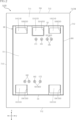
- FIG. 2 is a plan view of the semiconductor device shown in FIG.
- FIG. 3 is a right side view of the semiconductor device shown in FIG.
- FIG. 4 is a front view of the semiconductor device shown in FIG.
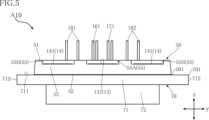
- FIG. 5 is a rear view of the semiconductor device shown in FIG.
- FIG. 6 is a bottom view of the semiconductor device shown in FIG.
- FIG. 7 is a plan view corresponding to FIG. 2, showing the sealing resin through which the heat dissipation member is omitted.
- FIG. 8 is a plan view corresponding to FIG. 2, showing the sealing resin through which the second conductive member and the heat dissipation member are omitted.
- FIG. 9 is a plan view corresponding to FIG.
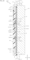
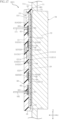
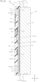
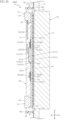
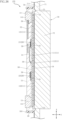
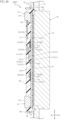
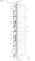
- FIG. 10 is a cross-sectional view taken along line XX in FIG.
- FIG. 11 is a cross-sectional view taken along line XI-XI in FIG.
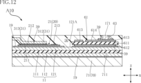
- FIG. 12 is a partial enlarged view of the first semiconductor element and its periphery shown in FIG.
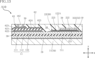
- FIG. 13 is a partial enlarged view of the second semiconductor element and its periphery shown in FIG.
- FIG. 14 is a cross-sectional view taken along line XIV-XIV in FIG.
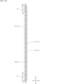
- FIG. 15 is a cross-sectional view taken along line XV-XV in FIG.
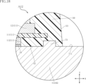
- FIG. 16 is a partially enlarged view of FIG. FIG.
- FIG. 17 is a cross-sectional view of a semiconductor device according to a first modified example of the first embodiment of the present disclosure, and corresponds to FIG.
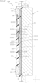
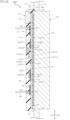
- FIG. 18 is a partially enlarged cross-sectional view of a semiconductor device according to a second modified example of the first embodiment of the present disclosure, and corresponds to FIG. 19A to 19C are cross-sectional views for explaining a manufacturing process of the semiconductor device shown in FIG. 20A to 20C are cross-sectional views for explaining the manufacturing process of the semiconductor device shown in FIG. 21A to 21C are cross-sectional views for explaining a manufacturing process of the semiconductor device shown in FIG. 22A to 22C are cross-sectional views illustrating a manufacturing process of the semiconductor device shown in FIG.
- FIG. 23A to 23C are cross-sectional views illustrating a manufacturing process of the semiconductor device shown in FIG. 24A to 24C are cross-sectional views illustrating a manufacturing process of the semiconductor device shown in FIG.
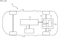
- FIG. 25 is a schematic diagram of a vehicle on which the semiconductor device shown in FIG. 1 is mounted.
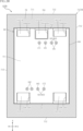
- FIG. 26 is a plan view of a semiconductor device according to a second embodiment of the present disclosure.
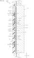
- FIG. 27 is a cross-sectional view of the semiconductor device shown in FIG. 26 and corresponds to FIG.
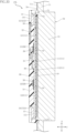
- FIG. 28 is a cross-sectional view of the semiconductor device shown in FIG. 26 and corresponds to FIG. 29 is a partially enlarged cross-sectional view illustrating a manufacturing process of the semiconductor device shown in FIG. FIG.
- FIG. 30 is a plan view of a semiconductor device according to a third embodiment of the present disclosure.
- FIG. 31 is a cross-sectional view of the semiconductor device shown in FIG. 30 and corresponds to FIG.
- FIG. 32 is a cross-sectional view of a semiconductor device according to a modified example of the third embodiment of the present disclosure, and corresponds to FIG. 33A to 33C are cross-sectional views illustrating a manufacturing process of the semiconductor device shown in FIG.
- FIG. 34 is a plan view of a semiconductor device according to a fourth embodiment of the present disclosure.
- FIG. 35 is a cross-sectional view of the semiconductor device shown in FIG. 34 and corresponds to FIG.
- FIG. 36 is a cross-sectional view of the semiconductor device shown in FIG. 34 and corresponds to FIG.
- FIG. 37A to 37C are cross-sectional views illustrating a manufacturing process of the semiconductor device shown in FIG. 38 is a cross-sectional view illustrating a manufacturing process of the semiconductor device shown in FIG.
- FIG. 39 is a plan view of a semiconductor device according to a fifth embodiment of the present disclosure.
- FIG. 40 is a cross-sectional view of the semiconductor device shown in FIG. 39 and corresponds to FIG.
- FIG. 41 is a cross-sectional view of the semiconductor device shown in FIG. 39 and corresponds to FIG. 42A to 42C are cross-sectional views illustrating a manufacturing process of the semiconductor device shown in FIG. 43A to 43C are cross-sectional views illustrating the manufacturing process of the semiconductor device shown in FIG.
- the semiconductor device A10 includes a base material 11, a first bonding layer 19, a first power terminal 13, two second power terminals 14, two third power terminals 15, a plurality of semiconductor elements 20, a first conductive member 31, a second conductive member 32, a second bonding layer 39, a sealing resin 50, and a heat dissipation member 70.
- the semiconductor device A10 further includes a first signal terminal 161, a second signal terminal 162, a third signal terminal 171, a fourth signal terminal 172, two fifth signal terminals 181, two sixth signal terminals 182, two thermistors 23, a first wiring 61, and a second wiring 62.
- the sealing resin 50 is shown through and the heat dissipation member 70 is omitted.
- the second conductive member 32 is further omitted from illustration in Fig. 8.
- the first conductive member 31 and the second conductive member 32 are further omitted from illustration in Fig. 9.
- the normal direction of the main surface 711 of the heat dissipation member 70 described later is referred to as the "first direction z.”
- the direction perpendicular to the first direction z is referred to as the "second direction x.”
- the direction perpendicular to both the first direction z and the second direction x is referred to as the "third direction y.”
- the semiconductor device A10 converts DC power input to the first power terminal 13 and the two second power terminals 14 into AC power using multiple semiconductor elements 20.
- the converted AC power is input from each of the two third power terminals 15 to a power supply target such as a motor.
- the heat dissipation member 70 is used to cool the semiconductor device A10.
- the heat dissipation member 70 contains metal.
- the heat dissipation member 70 is made of a material containing aluminum (Al), for example.
- the heat dissipation member 70 has a base 71, a main surface 711, multiple end surfaces 712, and a heat dissipation portion 72.
- the base 71 is flat.
- the main surface 711 and the multiple end surfaces 712 are included in the base 71.
- the main surface 711 faces one side of the first direction z.
- a portion of the main surface 711 is exposed from the sealing resin 50.
- Each of the multiple end surfaces 712 faces in a direction perpendicular to the first direction z.
- Each of the multiple end surfaces 712 is exposed from the sealing resin 50.
- the heat dissipation portion 72 is connected to the base portion 71.
- the heat dissipation portion 72 protrudes from the base portion 71 on the side opposite to the side to which the main surface 711 faces in the first direction z.
- the heat dissipation portion 72 is rectangular.
- the heat dissipation portion 72 may be a plurality of fins arranged in a direction perpendicular to the first direction z.
- the heat dissipation portion 72 when viewed in the first direction z, the heat dissipation portion 72 is located inward from the periphery 501 of the sealing resin 50.
- the base 71 of the heat dissipation member 70 has an engagement portion 73 recessed from the main surface 711. A portion of the sealing resin 50 is accommodated in the engagement portion 73.
- the heat dissipation member 70 has an inner circumferential surface 713 that is connected to the main surface 711 and defines the engagement portion 73.
- the inner circumferential surface 713 is included in the base 71.
- the sealing resin 50 is in contact with the inner circumferential surface 713.
- the sealing resin 50 covers the substrate 11, the first conductive layer 121, the second conductive layer 122, the semiconductor elements 20, the first conductive member 31 and the second conductive member 32. Furthermore, the sealing resin 50 covers a part of each of the first power terminal 13, the third power terminal 15 and the second power terminal 14.
- the sealing resin 50 has electrical insulation properties.
- the sealing resin 50 is made of a material containing, for example, a black epoxy resin.
- the sealing resin 50 when viewed in the first direction z, the sealing resin 50 is located inward from the periphery 701 of the heat dissipation member 70.
- the sealing resin 50 has a top surface 51, a bottom surface 52, a first side surface 53, a second side surface 54 and a plurality of recesses 55.
- the top surface 51 faces the side where the first conductive layer 121 and the second conductive layer 122 are located with the substrate 11 as the reference in the first direction z. That is, the top surface 51 faces the same side as the main surface 711 of the heat dissipation member 70 in the first direction z.
- the bottom surface 52 faces the opposite side to the top surface 51 in the first direction z. As shown in Figures 10, 11, 14, and 15, the bottom surface 52 is in contact with the main surface 711.
- the first side 53 and the second side 54 are spaced apart from each other in the second direction x.
- the first side 53 and the second side 54 face in opposite directions from each other in the second direction x.
- each of the multiple recesses 55 is recessed from the top surface 51 and either the first side surface 53 or the second side surface 54.
- the multiple recesses 55 include a first recess 55A, two second recesses 55B, and two third recesses 55C.
- the first recess 55A and the two second recesses 55B are each connected to the first side surface 53.
- the first recess 55A is located between the two second recesses 55B.
- the two third recesses 55C are connected to the second side surface 54.
- the two third recesses 55C are separated from each other in the third direction y.
- the substrate 11 is bonded to the main surface 711 of the heat dissipation member 70 as shown in Figures 10, 11, 14 and 15.
- the substrate 11 is composed of, for example, a DBC (Direct Bonded Copper) substrate.
- the substrate 11 has an insulating layer 111, a metal layer 112, a first conductive layer 121 and a second conductive layer 122.
- the substrate 11 is covered with a sealing resin 50.
- the metal layer 112 is bonded to the main surface 711 of the heat dissipation member 70.
- the metal layer 112 contains copper (Cu). When viewed in the first direction z, the metal layer 112 is located inward from the periphery 111A of the insulating layer 111.
- the insulating layer 111 is located between the metal layer 112 and the first and second conductive layers 121 and 122 in the first direction z. That is, the insulating layer 111 is located between the main surface 711 of the heat dissipation member 70 and the first and second conductive layers 121 and 122.
- the metal layer 112 is also bonded to the insulating layer 111.
- the insulating layer 111 is made of a material with relatively high thermal conductivity.
- the insulating layer 111 is made of ceramics containing aluminum nitride (AlN), for example.
- the insulating layer 111 may be made of an insulating resin sheet in addition to ceramics.
- the first conductive layer 121 and the second conductive layer 122 are located on the opposite side of the insulating layer 111 to the metal layer 112. Each of the first conductive layer 121 and the second conductive layer 122 is bonded to the insulating layer 111. As shown in Figures 8 and 9, each of the first conductive layer 121 and the second conductive layer 122 is located inward from the periphery 111A of the insulating layer 111. Each of the first conductive layer 121 and the second conductive layer 122 contains copper. The first conductive layer 121 and the second conductive layer 122 are spaced apart from each other in the second direction x.
- the dimension of each of the first conductive layer 121 and the second conductive layer 122 in the first direction z is greater than the dimension of the insulating layer 111 in the first direction z.
- the first conductive layer 121 has a first mounting surface 121A that faces the same side as the main surface 711 of the heat dissipation member 70 in the first direction z.
- the first mounting surface 121A faces the multiple semiconductor elements 20.
- the second conductive layer 122 has a second mounting surface 122A that faces the same side as the first mounting surface 121A in the first direction z.
- the first bonding layer 19 bonds the main surface 711 of the heat dissipation member 70 to the metal layer 112, as shown in Figures 10, 11, 14, and 15.
- the first bonding layer 19 is covered with the sealing resin 50.
- the first bonding layer 19 contains a metal.
- the first bonding layer 19 is a sintered body of metal particles containing silver (Ag) or the like.
- the first bonding layer 19 may be a minute metal layer (hereinafter referred to as a "solid-phase diffusion layer”) located at the bonding interface formed by solid-phase diffusion.
- the first bonding layer 19 may be a metal layer formed by brazing using silver or the like.
- the glass transition point of the sealing resin 50 is lower than the melting point of the first bonding layer 19.
- each of the multiple semiconductor elements 20 is mounted on either the first conductive layer 121 or the second conductive layer 122.
- the multiple semiconductor elements 20 are, for example, MOSFETs (Metal-Oxide-Semiconductor Field-Effect Transistors).
- the multiple semiconductor elements 20 may be switching elements such as IGBTs (Insulated Gate Bipolar Transistors) or diodes.
- IGBTs Insulated Gate Bipolar Transistors
- the multiple semiconductor elements 20 are n-channel type MOSFETs with a vertical structure.
- the multiple semiconductor elements 20 include a compound semiconductor substrate.
- the compound semiconductor substrate includes silicon carbide (SiC).
- the multiple semiconductor elements 20 include multiple first semiconductor elements 21 and multiple second semiconductor elements 22.
- the structure of each of the multiple second semiconductor elements 22 is equal to the structure of each of the multiple first semiconductor elements 21.
- the multiple first semiconductor elements 21 are mounted on a first mounting surface 121A of the first conductive layer 121.
- the multiple first semiconductor elements 21 are arranged along the third direction y.
- the multiple second semiconductor elements 22 are mounted on a second mounting surface 122A of the second conductive layer 122.
- the multiple second semiconductor elements 22 are arranged along the third direction y.
- each of the multiple first semiconductor elements 21 has a first electrode 211, a second electrode 212, a first gate electrode 213, and a first detection electrode 214.
- the first electrode 211 faces the first mounting surface 121A of the first conductive layer 121.
- a current corresponding to the power before being converted by the first semiconductor element 21 flows through the first electrode 211.
- the first electrode 211 corresponds to the drain electrode of the first semiconductor element 21.
- the first electrode 211 is conductively bonded to the first mounting surface 121A via the first bonding layer 19.
- the first electrode 211 of each of the multiple first semiconductor elements 21 is electrically connected to the first conductive layer 121.
- the second electrode 212 is located on the opposite side of the first conductive layer 121 facing the first mounting surface 121A in the first direction z. Therefore, the first electrode 211 and the second electrode 212 are located on opposite sides of each other in the first direction z. A current corresponding to the power converted by the first semiconductor element 21 flows through the second electrode 212. In other words, the second electrode 212 corresponds to the source electrode of the first semiconductor element 21.
- the first gate electrode 213 is located on the opposite side of the first conductive layer 121 facing the first mounting surface 121A in the first direction z. Therefore, the first gate electrode 213 is located on the same side as the second electrode 212 in the first direction z.
- a gate voltage for driving the first semiconductor element 21 is applied to the first gate electrode 213.
- the area of the first gate electrode 213 is smaller than the area of the second electrode 212 when viewed in the first direction z.
- the first detection electrode 214 is located on the same side as the second electrode 212 and the first gate electrode 213 in the first direction z.
- the first detection electrode 214 is located next to the first gate electrode 213 in the third direction y.
- a voltage equivalent to the voltage applied to the second electrode 212 is applied to the first detection electrode 214.
- the area of the first detection electrode 214 is equal (or approximately equal) to the area of the first gate electrode 213.
- each of the multiple second semiconductor elements 22 has a third electrode 221, a fourth electrode 222, a second gate electrode 223, and a second detection electrode 224.
- the third electrode 221 faces the second mounting surface 122A of the second conductive layer 122.
- a current corresponding to the power before being converted by the second semiconductor element 22 flows through the third electrode 221.
- the third electrode 221 corresponds to the drain electrode of the second semiconductor element 22.
- the third electrode 221 is conductively bonded to the second mounting surface 122A via the first bonding layer 19.
- the third electrode 221 of each of the multiple second semiconductor elements 22 is conductive to the second conductive layer 122.
- the fourth electrode 222 is located on the opposite side of the second conductive layer 122 facing the second mounting surface 122A in the first direction z. Therefore, the third electrode 221 and the fourth electrode 222 are located on opposite sides of each other in the first direction z. A current corresponding to the power converted by the second semiconductor element 22 flows through the fourth electrode 222. In other words, the fourth electrode 222 corresponds to the source electrode of the second semiconductor element 22.
- the second gate electrode 223 is located on the opposite side of the second conductive layer 122 facing the second mounting surface 122A in the first direction z. Therefore, the second gate electrode 223 is located on the same side as the fourth electrode 222 in the first direction z.
- a gate voltage for driving the second semiconductor element 22 is applied to the second gate electrode 223. As shown in FIG. 9, the area of the second gate electrode 223 is smaller than the area of the fourth electrode 222 when viewed in the first direction z.
- the second detection electrode 224 is located on the same side as the fourth electrode 222 and the second gate electrode 223 in the first direction z.
- the second detection electrode 224 is located on both sides of the second gate electrode 223 in the third direction y.
- a voltage equivalent to the voltage applied to the fourth electrode 222 is applied to the second detection electrode 224.
- the area of the second detection electrode 224 is equal (or approximately equal) to the area of the second gate electrode 223.
- the first power terminal 13 is located on the opposite side of the second semiconductor elements 22 with respect to the first semiconductor elements 21 in the second direction x.
- the first power terminal 13 is disposed on the substrate 11.
- the first power terminal 13 is conductively bonded to the first conductive layer 121.
- the first power terminal 13 is electrically connected to the first electrodes 211 of the first semiconductor elements 21 via the first conductive layer 121.
- the first power terminal 13 is a P terminal (positive electrode) to which DC power to be converted is input. As shown in FIG. 2, the first power terminal 13 is exposed from the top surface 51 of the sealing resin 50.
- the first power terminal 13 When viewed in the first direction z, the first power terminal 13 is surrounded by the periphery 501 of the sealing resin 50 and is located inward from the periphery of the top surface 51. As shown in FIG. 11, the first power terminal 13 has a first connection surface 131 exposed from the sealing resin 50. The first connection surface 131 faces the same side as the main surface 711 of the heat dissipation member 70 in the first direction z. As shown in FIG. 5 and FIG. 11, in the semiconductor device A10, the first connection surface 131 is accommodated in the first recess 55A among the multiple recesses 55 in the sealing resin 50. In addition to the configuration of the first power terminal 13 in the semiconductor device A10, the first power terminal 13 may be configured to protrude from the first side surface 53 of the sealing resin 50 in the second direction x.
- each of the two second power terminals 14 is located on the same side as the first power terminal 13 with respect to the multiple first semiconductor elements 21 in the second direction x.
- the two second power terminals 14 are arranged on the substrate 11.
- Each of the two second power terminals 14 is arranged on the insulating layer 111.
- Each of the two second power terminals 14 is electrically connected to the fourth electrode 222 of each of the multiple second semiconductor elements 22.
- the two second power terminals 14 are N terminals (negative electrodes) to which DC power to be converted is input.
- the second power terminals 14 are separated from each other in the third direction y.
- the first power terminal 13 is located between the two second power terminals 14 in the third direction y. As shown in FIG.
- each of the two second power terminals 14 is exposed from the top surface 51 of the sealing resin 50. As viewed in the first direction z, each of the two second power terminals 14 is surrounded by the periphery 501 of the sealing resin 50 and is located inward from the periphery of the top surface 51. As shown in FIG. 10, each of the two second power terminals 14 has a second connection surface 141 exposed from the sealing resin 50. The second connection surface 141 faces the same side as the main surface 711 of the heat dissipation member 70 in the first direction z. As shown in FIG. 5 and FIG. 10, in the semiconductor device A10, the two second connection surfaces 141 are individually accommodated in two second recesses 55B among the multiple recesses 55 of the sealing resin 50. In addition to the configuration of the two second power terminals 14 in the semiconductor device A10, the configuration of the two second power terminals 14 each protruding from the first side surface 53 of the sealing resin 50 in the second direction x may be used.
- each of the two third power terminals 15 is located on the opposite side of the first power terminal 13 and the two second power terminals 14 in the second direction x with respect to the multiple semiconductor elements 20.
- the two third power terminals 15 are arranged on the substrate 11.
- Each of the two third power terminals 15 is conductively bonded to the second conductive layer 122.
- each of the two third power terminals 15 is electrically connected to the third electrodes 221 of the multiple second semiconductor elements 22 via the second conductive layer 122.
- AC power converted by the multiple semiconductor elements 20 is output from each of the two third power terminals 15.
- the two third power terminals 15 are separated from each other in the third direction y. As shown in FIG.
- each of the two third power terminals 15 is exposed from the top surface 51 of the sealing resin 50. As viewed in the first direction z, each of the two third power terminals 15 is surrounded by the periphery 501 of the sealing resin 50 and is located inward from the periphery of the top surface 51. As shown in FIG. 10, each of the two third power terminals 15 has a third connection surface 151 exposed from the sealing resin 50. The third connection surface 151 faces the same side as the main surface 711 of the heat dissipation member 70 in the first direction z. As shown in FIG. 4 and FIG. 10, in the semiconductor device A10, the two third connection surfaces 151 are individually accommodated in two third recesses 55C among the multiple recesses 55 of the sealing resin 50. In addition to the configuration of the two third power terminals 15 in the semiconductor device A10, the configuration of two third power terminals 15 each protruding from the second side surface 54 of the sealing resin 50 in the second direction x may be used.
- the first wiring 61 is bonded to the first mounting surface 121A of the first conductive layer 121, as shown in FIG. 12.
- the first wiring 61 is located on the opposite side of the multiple second semiconductor elements 22 with respect to the multiple first semiconductor elements 21 in the second direction x.
- the first wiring 61 is electrically connected to the multiple first semiconductor elements 21 and the first conductive layer 121.
- the first wiring 61 has a first mounting layer 611, a first metal layer 612, two first gate wiring layers 613, a first detection wiring layer 614, a first temperature detection wiring layer 615, and a second detection wiring layer 616.
- the first mounting layer 611 includes two first gate wiring layers 613, a first detection wiring layer 614, two first temperature detection wiring layers 615, and a second detection wiring layer 616.
- the first mounting layer 611 is an insulator.
- the first mounting layer 611 is made of ceramics, for example. Alternatively, the first mounting layer 611 may be made of an insulating resin sheet.
- the first metal layer 612 is located on the side facing the first mounting surface 121A of the first conductive layer 121 with the first mounting layer 611 as a reference in the first direction z.
- the first metal layer 612 is bonded to the first mounting layer 611.
- the first metal layer 612 contains copper.
- the first metal layer 612 is bonded to the first mounting surface 121A via the second bonding layer 39.
- the second bonding layer 39 contains a metal.
- the second bonding layer 39 is solder. Therefore, the second bonding layer 39 contains tin (Sn).
- the second bonding layer 39 may be a sintered body of metal particles containing silver (Ag) or the like.
- the glass transition point of the sealing resin 50 is lower than the melting point of the second bonding layer 39.
- the melting point of the second bonding layer 39 is lower than the melting point of the first bonding layer 19.
- the two first gate wiring layers 613 are located on the opposite side of the first metal layer 612 with respect to the first mounting layer 611.
- the two first gate wiring layers 613 are bonded to the first mounting layer 611.
- one of the first gate wiring layers 613 has a plurality of first wires 41 conductively bonded thereto.
- the plurality of first wires 41 are individually conductively bonded to the first gate electrodes 213 of the plurality of first semiconductor elements 21.
- a plurality of sixth wires 46 are conductively bonded to each of the two first gate wiring layers 613.
- each of the two first gate wiring layers 613 is electrically connected to the first gate electrodes 213 of the plurality of first semiconductor elements 21.
- the first detection wiring layer 614 is located on the opposite side of the first metal layer 612 with respect to the first mounting layer 611.
- the first detection wiring layer 614 is bonded to the first mounting layer 611.
- a plurality of second wires 42 are conductively bonded to the first detection wiring layer 614.
- the plurality of second wires 42 are individually conductively bonded to the first detection electrodes 214 of each of the plurality of first semiconductor elements 21.
- the first detection wiring layer 614 is electrically connected to the first detection electrodes 214 of each of the plurality of first semiconductor elements 21.
- the two first temperature detection wiring layers 615 are located on the opposite side of the first metal layer 612 with respect to the first mounting layer 611.
- the two first temperature detection wiring layers 615 are bonded to the first mounting layer 611.
- the two first temperature detection wiring layers 615 are adjacent to each other in the third direction y.
- the second detection wiring layer 616 is located on the opposite side of the first mounting layer 611 from the first metal layer 612.
- the second detection wiring layer 616 is bonded to the first mounting layer 611.
- the second wiring 62 is joined to the second mounting surface 122A of the second conductive layer 122, as shown in FIG. 13.
- the second wiring 62 is located on the opposite side of the multiple first semiconductor elements 21 with respect to the multiple second semiconductor elements 22 in the second direction x.
- the second wiring 62 is electrically connected to the multiple second semiconductor elements 22 and the second conductive layer 122.
- the second wiring 62 has a second mounting layer 621, a second metal layer 622, two second gate wiring layers 623, a third detection wiring layer 624, two second temperature detection wiring layers 625, and a fourth detection wiring layer 626.
- the second mounting layer 621 includes two second gate wiring layers 623, a third detection wiring layer 624, two second temperature detection wiring layers 625, and a fourth detection wiring layer 626.
- the second mounting layer 621 is an insulator.
- the second mounting layer 621 is made of ceramics, for example. Alternatively, the second mounting layer 621 may be made of an insulating resin sheet.
- the second metal layer 622 is located on the side facing the second mounting surface 122A of the second conductive layer 122 with the second mounting layer 621 as a reference in the first direction z.
- the second metal layer 622 is bonded to the second mounting layer 621.
- the second metal layer 622 contains copper.
- the second metal layer 622 is bonded to the second mounting surface 122A via the second bonding layer 39.
- the two second gate wiring layers 623 are located on the opposite side of the second metal layer 622 with respect to the second mounting layer 621.
- the two second gate wiring layers 623 are bonded to the second mounting layer 621.
- one of the second gate wiring layers 623 has a plurality of fourth wires 44 conductively bonded thereto.
- the plurality of fourth wires 44 are individually conductively bonded to the second gate electrodes 223 of the plurality of second semiconductor elements 22.
- a plurality of seventh wires 47 are conductively bonded to each of the two second gate wiring layers 623.
- each of the two second gate wiring layers 623 is electrically connected to the second gate electrodes 223 of the plurality of second semiconductor elements 22.
- the third detection wiring layer 624 is located on the opposite side to the second metal layer 622 with respect to the second mounting layer 621.
- the third detection wiring layer 624 is bonded to the second mounting layer 621.
- a plurality of fifth wires 45 are conductively bonded to the third detection wiring layer 624.
- the plurality of fifth wires 45 are individually conductively bonded to the second detection electrodes 224 of each of the plurality of second semiconductor elements 22.
- the third detection wiring layer 624 is electrically connected to the second detection electrodes 224 of each of the plurality of second semiconductor elements 22.
- the two second temperature detection wiring layers 625 are located on the opposite side of the second metal layer 622 with respect to the second mounting layer 621.
- the two second temperature detection wiring layers 625 are bonded to the second mounting layer 621.
- the two second temperature detection wiring layers 625 are adjacent to each other in the third direction y.
- the fourth detection wiring layer 626 is located on the opposite side of the second metal layer 622 with respect to the second mounting layer 621.
- the fourth detection wiring layer 626 is bonded to the second mounting layer 621.
- each of the multiple sleeves 63 is conductively bonded to either the first wiring 61 or the second wiring 62 via the second bonding layer 39.
- the second bonding layer 39 is, for example, solder.
- the multiple sleeves 63 are made of a conductive material such as metal.
- Each of the multiple sleeves 63 is cylindrical and extends in the first direction z.
- each of the multiple sleeves 63 has an end surface 631 that faces the same side as the first mounting surface 121A of the first conductive layer 121 in the first direction z. The end surface 631 is exposed from the top surface 51 of the sealing resin 50, which will be described later.
- One of the two thermistors 23 is conductively joined to the two first temperature detection wiring layers 615 of the first wiring 61, as shown in Figures 8 and 9.
- the other of the two thermistors 23 is conductively joined to the two second temperature detection wiring layers 625 of the second wiring 62, as shown in Figures 8 and 9.
- the two thermistors 23 are used as temperature detection sensors for the semiconductor device A10.
- each of the first signal terminal 161, the second signal terminal 162, the third signal terminal 171, the fourth signal terminal 172, the two fifth signal terminals 181, and the two sixth signal terminals 182 is made of a metal pin extending in the first direction z. These terminals protrude from the top surface 51 of the sealing resin 50, which will be described later. Furthermore, these terminals are individually press-fitted into a number of sleeves 63. As a result, each of these terminals is supported by one of the multiple sleeves 63 and is conductive to one of the first wiring 61 and the second wiring 62.
- the first signal terminal 161 is press-fitted into one of the multiple sleeves 63 that is conductively joined to one of the two first gate wiring layers 613 of the first wiring 61.
- the first signal terminal 161 is electrically connected to the first gate electrode 213 of each of the multiple first semiconductor elements 21 via the two first gate wiring layers 613.
- a gate voltage for driving the multiple first semiconductor elements 21 is applied to the first signal terminal 161.
- the second signal terminal 162 is press-fitted into one of the multiple sleeves 63 that is conductively joined to one of the two second gate wiring layers 623 of the second wiring 62.
- the second signal terminal 162 is electrically connected to the second gate electrodes 223 of the multiple second semiconductor elements 22 via the two second gate wiring layers 623.
- a gate voltage for driving the multiple second semiconductor elements 22 is applied to the second signal terminal 162.
- the third signal terminal 171 is located next to the first signal terminal 161 in the third direction y. As shown in FIG. 9 and FIG. 11, the third signal terminal 171 is press-fitted into one of the multiple sleeves 63 that is conductively joined to the first detection wiring layer 614 of the first wiring 61. As a result, the third signal terminal 171 is electrically connected to the first detection electrode 214 of each of the multiple first semiconductor elements 21 via the first detection wiring layer 614. A voltage equivalent to the voltage applied to the first detection electrode 214 of each of the multiple first semiconductor elements 21 is applied to the third signal terminal 171.
- the fourth signal terminal 172 is located next to the second signal terminal 162 in the third direction y. As shown in FIG. 9, the fourth signal terminal 172 is press-fitted into one of the multiple sleeves 63 that is conductively joined to the third detection wiring layer 624 of the second wiring 62. As a result, the fourth signal terminal 172 is electrically connected to the second detection electrodes 224 of each of the multiple second semiconductor elements 22 via the third detection wiring layer 624. A voltage equivalent to the voltage applied to the second detection electrodes 224 of each of the multiple second semiconductor elements 22 is applied to the fourth signal terminal 172.
- the two fifth signal terminals 181 are located on the opposite side of the third signal terminal 171 with respect to the first signal terminal 161 in the third direction y.
- the two fifth signal terminals 181 are adjacent to each other in the third direction y.
- the two fifth signal terminals 181 are individually press-fitted into two of the multiple sleeves 63 that are individually conductively joined to the two first temperature detection wiring layers 615 of the first wiring 61.
- the two fifth signal terminals 181 are electrically connected to the two thermistors 23 that are conductively joined to the two first temperature detection wiring layers 615 of the two thermistors 23.
- the two sixth signal terminals 182 are located on the opposite side of the fourth signal terminal 172 in the third direction y with respect to the second signal terminal 162.
- the two sixth signal terminals 182 are adjacent to each other in the third direction y.
- the two sixth signal terminals 182 are individually press-fitted into two of the multiple sleeves 63 that are individually conductively joined to the two second temperature detection wiring layers 625 of the second wiring 62.
- the two sixth signal terminals 182 are electrically connected to the two thermistors 23 that are conductively joined to the two second temperature detection wiring layers 625 of the two thermistors 23.
- the first conductive member 31 is conductively joined to the second electrodes 212 of the multiple first semiconductor elements 21 and the second mounting surface 122A of the second conductive layer 122. As a result, the second electrodes 212 of the multiple first semiconductor elements 21 are electrically connected to the second conductive layer 122.
- the first conductive member 31 contains copper.
- the first conductive member 31 is a metal clip. As shown in Fig. 5, the first conductive member 31 has a main portion 311, multiple first joint portions 312, multiple first connecting portions 313, second joint portions 314 and second connecting portions 315.
- the main portion 311 forms the main part of the first conductive member 31. As shown in FIG. 8, the main portion 311 extends in the third direction y. The main portion 311 spans between the first conductive layer 121 and the second conductive layer 122.
- the multiple first bonding portions 312 are individually bonded to the second electrodes 212 of the multiple first semiconductor elements 21. Each of the multiple first bonding portions 312 faces the second electrodes 212 of one of the multiple first semiconductor elements 21.
- the multiple first connecting portions 313 are connected to the main portion 311 and the multiple first bonding portions 312.
- the multiple first connecting portions 313 are spaced apart from one another in the third direction y.
- the multiple first connecting portions 313 are inclined in a direction away from the first mounting surface 121A of the first conductive layer 121 as they move from the multiple first bonding portions 312 toward the main portion 311.
- the second joint 314 is joined to the second mounting surface 122A of the second conductive layer 122.
- the second joint 314 faces the second mounting surface 122A.
- the second joint 314 extends in the third direction y.
- the dimension of the second joint 314 in the third direction y is equal to the dimension of the main portion 311 in the third direction y.
- the second connecting portion 315 is connected to the main portion 311 and the second joint portion 314.
- the second connecting portion 315 is inclined in a direction away from the second mounting surface 122A of the second conductive layer 122 as it moves from the second joint portion 314 toward the main portion 311.
- the dimension of the second connecting portion 315 in the third direction y is equal to the dimension of the main portion 311 in the third direction y.
- a second bonding layer 39 is located between the second electrode 212 of each of the multiple first semiconductor elements 21 and each of the multiple first bonding portions 312.
- the second bonding layer 39 conductively bonds each of the multiple first bonding portions 312 to the second electrode 212 of each of the multiple first semiconductor elements 21 individually.
- the second bonding layer 39 is, for example, solder.
- a second bonding layer 39 is located between the second mounting surface 122A of the second conductive layer 122 and the second bonding portion 314.
- the second bonding layer 39 conductively bonds the second mounting surface 122A to the second bonding portion 314.
- the second conductive member 32 is conductively joined to the second electrodes 212 of the multiple second semiconductor elements 22 and the two second power terminals 14. As a result, the second electrodes 212 of the multiple second semiconductor elements 22 are electrically connected to the second power terminals 14.
- the second conductive member 32 contains copper.
- the second conductive member 32 is a metal clip. As shown in Fig. 7, the second conductive member 32 has two main portions 321, multiple third joint portions 322, multiple third connecting portions 323, multiple intermediate portions 326, and a cross beam portion 327.
- the two main parts 321 are spaced apart from each other in the third direction y.
- the two main parts 321 extend in the second direction x.
- the two main parts 321 are arranged parallel to the first mounting surface 121A of the first conductive layer 121 and the second mounting surface 122A of the second conductive layer 122.
- the two main parts 321 are spaced apart from the first mounting surface 121A and the second mounting surface 122A more than the main part 311 of the first conductive member 31.
- the multiple intermediate portions 326 are spaced apart from each other in the third direction y and are located between the two main portions 321 in the third direction y.
- the multiple intermediate portions 326 extend in the second direction x.
- the dimension of each of the multiple intermediate portions 326 in the second direction x is smaller than the dimension of each of the two main portions 321 in the second direction x.
- the multiple third bonding portions 322 are individually bonded to the second electrodes 212 of the multiple second semiconductor elements 22. Each of the multiple third bonding portions 322 faces the fourth electrode 222 of one of the multiple second semiconductor elements 22.
- the multiple third connecting parts 323 are connected to both sides of the multiple third joint parts 322 in the third direction y. Furthermore, the multiple third connecting parts 323 are connected to either of the two main parts 321 or the multiple intermediate parts 326. When viewed in the second direction x, each of the multiple third connecting parts 323 is inclined in a direction away from the second mounting surface 122A of the second conductive layer 122 as it moves from one of the multiple third joint parts 322 toward one of the two main parts 321 or the multiple intermediate parts 326.
- the cross beam portion 327 extends in the third direction y. As shown in FIG. 15, when viewed in the first direction z, the cross beam portion 327 includes an area that overlaps with each of the multiple first joint portions 312 of the first conductive member 31. Both sides of the cross beam portion 327 in the third direction y are individually connected to the two main portions 321.
- a second bonding layer 39 is located between the fourth electrode 222 of each of the multiple second semiconductor elements 22 and each of the multiple third bonding portions 322.
- the second bonding layer 39 conductively bonds each of the multiple third bonding portions 322 to the fourth electrode 222 of each of the multiple second semiconductor elements 22 individually.
- a second bonding layer 39 is located between the two second power terminals 14 and the two main portions 321.
- the second bonding layer 39 conductively bonds each of the two second power terminals 14 to the two main portions 321 individually.
- FIG. 17 corresponds to FIG. 11 showing the semiconductor device A10.
- the configuration relating to the conductive bonding of each of the multiple semiconductor elements 20 to either the first conductive layer 121 or the second conductive layer 122 is different from that of the semiconductor device A10.
- the first electrode 211 of each of the multiple first semiconductor elements 21 is conductively bonded to the first mounting surface 121A of the first conductive layer 121 via the second bonding layer 39.
- the third electrodes 221 of the multiple second semiconductor elements 22 are conductively bonded to the second mounting surface 122A of the second conductive layer 122 via the second bonding layer 39.
- FIG. 18 corresponds to FIG. 16 showing the semiconductor device A10.
- the configuration of the engagement portion 73 of the heat dissipation member 70 differs from that of the semiconductor device A10.
- the engagement portion 73 protrudes from the main surface 711 of the heat dissipation member 70.
- the engagement portion 73 is recessed into the sealing resin 50.
- Figures 19 to 22 correspond to Figure 10, which shows semiconductor device A10.
- the first conductive layer 121 and the second conductive layer 122 are each bonded to one side of the insulating layer 111 in the first direction z. Additionally, the metal layer 112 is bonded to the other side of the insulating layer 111 in the first direction z. Thereafter, the first power terminal 13 is conductively bonded to the first conductive layer 121 (see FIG. 11). Each of the two second power terminals 14 is disposed on the insulating layer 111. Each of the two third power terminals 15 is conductively bonded to the second conductive layer 122. This process is performed at least before the fourth process P4 described below.
- the first process P1 is performed to bond the substrate 11 to the heat dissipation member 70.
- the metal layer 112 is bonded to the main surface 711 of the heat dissipation member 70 via the first bonding layer 19.
- the temperature at which the first bonding layer 19 is formed in the first process P1 is, for example, 200°C or higher and 600°C or lower.
- the second process P2 is performed to conductively bond each of the multiple semiconductor elements 20 to either the first conductive layer 121 or the second conductive layer 122.
- the second process P2 is performed simultaneously with the first process P1.
- Each of the multiple semiconductor elements 20 is conductively bonded to either the first conductive layer 121 or the second conductive layer 122 via the first bonding layer 19.
- the first bonding layer 19 is formed by sintering metal particles containing silver or the like.
- the first bonding layer 19 may be a solid-phase bonding layer. When forming the solid-phase bonding layer, pressure is applied to the substrate 11 and each of the multiple semiconductor elements 20 in the first direction z toward the side facing the main surface 711 of the heat dissipation member 70.
- a fourth process P4 is performed in which the first conductive member 31 and the second conductive member 32 are conductively bonded to each of the first semiconductor elements 21 and the second conductive layer 122 via the second bonding layer 39.
- the second conductive member 32 is conductively bonded to each of the second semiconductor elements 22 and the two second power terminals 14 via the second bonding layer 39.
- the first wiring 61 to which the thermistor 23 and the multiple sleeves 63 are conductively bonded is bonded to the first conductive layer 121 via the second bonding layer 39 (see FIG. 11).
- the second wiring 62 to which the thermistor 23 and the multiple sleeves 63 are conductively bonded is bonded to the second conductive layer 122 via the second bonding layer 39 (see FIG. 11).
- the first wires 41, the second wires 42, the fourth wires 44, the fifth wires 45, the sixth wires 46, and the seventh wires 47 are each formed.
- the temperature at which the second bonding layer 39 is formed in the fourth process P4 is, for example, about 260° C.
- the second bonding layer 39 is formed by melting the solder by reflow and then solidifying the solder.
- the third process P3 is performed to form the sealing resin 50 that covers the semiconductor elements 20.
- the substrate 11, the first conductive member 31, and the second conductive member 32 are covered with the sealing resin 50.
- the sealing resin 50 is formed by transfer molding.
- the third process P3 is performed after the first process P1, the second process P2, and the fourth process P4 are each completed.
- the temperature at which the sealing resin 50 is formed in the third process P3 is, for example, about 180°C. Therefore, the temperature at which the sealing resin 50 is formed in the third process P3 is lower than the temperature at which the first bonding layer 19 is formed in the first process P1 and the temperature at which the second bonding layer 39 is formed in the fourth process P4.
- the bottom surface 52 of the sealing resin 50 is brought into contact with the main surface 711 of the heat dissipation member 70.
- each of the multiple end surfaces 712 of the heat dissipation member 70 is exposed from the sealing resin 50.
- the sealing resin 50 is positioned inward from the periphery 701 of the heat dissipation member 70.
- the first power terminal 13, the two second power terminals 14, and the two third power terminals 15 are each exposed from the top surface 51 of the sealing resin 50. Furthermore, the sealing resin 50 is recessed into the engagement portion 73 provided on the heat dissipation member 70.
- the first signal terminal 161, the second signal terminal 162, the third signal terminal 171, the fourth signal terminal 172, the two fifth signal terminals 181, and the two sixth signal terminals 182 are each individually inserted into the multiple sleeves 63. This causes these signal terminals to protrude from the top surface 51 of the sealing resin 50. This process is performed after the third process P3 is completed. Through the above processes, the semiconductor device A10 is obtained.
- Figures 23 and 24 correspond to Figure 10, which shows the semiconductor device A10.
- the method for manufacturing the semiconductor device A11 differs from the method for manufacturing the semiconductor device A10 in the order of the first process P1, the second process P2, and the fourth process P4.
- the first process P1 shown in FIG. 23 is performed.
- the second process P2 and the fourth process P4 are performed simultaneously as shown in FIG. 24.
- Each of the multiple semiconductor elements 20 is conductively bonded to either the first conductive layer 121 or the second conductive layer 122 via the second bonding layer 39.
- the third process P3 shown in FIG. 22 is performed.
- the vehicle B is, for example, an electric vehicle (EV).
- EV electric vehicle
- vehicle B is equipped with an on-board charger 81, a storage battery 82, and a drive system 83.
- Power is supplied to the on-board charger 81 wirelessly from a power supply facility (not shown) installed outdoors. Alternatively, power may be supplied from the power supply facility to the on-board charger 81 via a wired connection.
- the on-board charger 81 is configured with a step-up DC-DC converter. The voltage of the power supplied to the on-board charger 81 is stepped up by the converter and then supplied to the storage battery 82. The stepped-up voltage is, for example, 600V.
- the drive system 83 drives the vehicle B.
- the drive system 83 has an inverter 831 and a drive source 832.
- the semiconductor device A10 constitutes part of the inverter 831.
- the power stored in the storage battery 82 is supplied to the inverter 831.
- the power supplied from the storage battery 82 to the inverter 831 is DC power.
- a step-up DC-DC converter may be further provided between the storage battery 82 and the inverter 831.
- the inverter 831 converts DC power into AC power.
- the inverter 831 including the semiconductor device A10 is conducted to the drive source 832.
- the drive source 832 has an AC motor and a transmission.
- the AC motor rotates and the rotation is transmitted to the transmission.
- the transmission rotates the drive shaft of the vehicle B after appropriately reducing the rotation speed transmitted from the AC motor. This drives vehicle B.
- semiconductor device A10 in inverter 831 is necessary to output AC power with an appropriate frequency change to correspond to the required rotation speed of the AC motor.
- the manufacturing method of the semiconductor device A10 includes a first process P1, a second process P2, and a third process P3.
- a substrate 11 having an insulating layer 111, a first conductive layer 121, and a second conductive layer 122 is bonded to a heat dissipation member 70.
- a semiconductor element 20 is bonded to either the first conductive layer 121 or the second conductive layer 122.
- a sealing resin 50 is formed to cover the semiconductor element 20.
- the substrate 11 is bonded to the heat dissipation member 70 such that the insulating layer 111 is positioned between the heat dissipation member 70 and the first conductive layer 121 and the second conductive layer 122.
- the third process P3 is performed after the first process P1 and the second process P2 are each completed.
- the first step P1 is completed at the time of the third step P3, so the semiconductor device A10 being manufactured after the third step P3 is not placed in a hotter environment than the temperature at which the sealing resin 50 is formed. Therefore, with this configuration, the shape of the sealing resin 50 can be better maintained in the manufacturing method of the semiconductor device A10 in which the base material 11 is bonded to the heat dissipation member 70.
- the substrate 11 is bonded to the main surface 711 of the heat dissipation member 70 via the first bonding layer 19.
- the temperature at which the sealing resin 50 is formed in the third process P3 is lower than the temperature at which the first bonding layer 19 is formed in the first process P1.
- the manufacturing method of the semiconductor device A10 further includes a fourth process P4 in which the second conductive member 32 is conductively bonded to the semiconductor element 20 (second semiconductor element 22) via the second bonding layer 39.
- the fourth process P4 is performed before the third process P3.
- the temperature at which the sealing resin 50 is formed in the third process P3 is lower than the temperature at which the second bonding layer 39 is formed in the fourth process P4. This configuration makes it possible to prevent the second bonding layer 39 from melting when the sealing resin 50 is formed.
- the sealing resin 50 is brought into contact with the main surface 711 of the heat dissipation member 70. Additionally, the base material 11 is covered with the sealing resin 50, and the end surface 712 of the heat dissipation member 70 is exposed from the sealing resin 50. Furthermore, when viewed in the first direction z, the sealing resin 50 is positioned inward from the periphery 701 of the heat dissipation member 70. With this configuration, when forming the sealing resin 50 in the third process P3, the molding die can be pressed against the heat dissipation member 70 without any gaps. This further improves the molding state of the sealing resin 50.
- the semiconductor device A10 further includes a first power terminal 13 that is electrically connected to the semiconductor element 20 (first semiconductor element 21).
- the first power terminal 13 is exposed from the top surface 51 of the sealing resin 50. When viewed in the first direction z, the first power terminal 13 is located inward from the periphery of the top surface 51. This configuration ensures a longer creepage distance (the distance along the surface of the sealing resin 50) from the first power terminal 13 to the heat dissipation member 70. This makes it possible to further improve the dielectric strength voltage of the semiconductor device A10.
- the heat dissipation member 70 has an engagement portion 73 recessed from the main surface 711.
- the sealing resin 50 is recessed into the engagement portion 73. This configuration causes the sealing resin 50 to have an anchor effect on the heat dissipation member 70. This makes it possible to prevent the sealing resin 50 from peeling off from the main surface 711.
- the semiconductor device A10 further includes a first signal terminal 161 that is electrically connected to the semiconductor element 20 (first semiconductor element 21).
- the first signal terminal 161 protrudes from the top surface 51 of the sealing resin 50. This configuration ensures a longer creepage distance from the first signal terminal 161 to the heat dissipation member 70.
- FIG. 26 A semiconductor device A20 according to a second embodiment of the present disclosure will be described with reference to Figures 26 to 28.
- elements that are the same as or similar to those of the semiconductor device A10 described above are given the same reference numerals, and duplicated descriptions will be omitted.
- Figure 27 corresponds to Figure 10 showing the semiconductor device A10.
- Figure 28 corresponds to Figure 11 showing the semiconductor device A10.
- semiconductor device A20 the configurations of the first power terminal 13, the two second power terminals 14, the two third power terminals 15, and the sealing resin 50 are different from those of semiconductor device A10.
- the first power terminal 13, the two second power terminals 14, and the two third power terminals 15 each protrude from the top surface 51 of the sealing resin 50.
- the sealing resin 50 does not have a plurality of recesses 55.
- the first connection surface 131 of the first power terminal 13, the second connection surface 141 of each of the two second power terminals 14, and the third connection surface 151 of each of the two third power terminals 15 are located on the opposite side of the bottom surface 52 of the sealing resin 50 with respect to the top surface 51 in the first direction z.
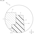
- FIG. 29 corresponds to a partially enlarged view of FIG. 28 showing semiconductor device A20.
- the manufacturing method for semiconductor device A20 differs from the manufacturing method for semiconductor device A10 in the third step P3.
- the third process P3 after forming the sealing resin 50, a portion of the sealing resin 50 located on one side in the first direction z is removed by a method such as wet blasting.
- the first power terminal 13, the two second power terminals 14, and the two third power terminals 15 each protrude from the top surface 51 of the sealing resin 50.
- the surface roughness of the top surface 51 of the sealing resin 50 is greater than the surface roughness of the first side surface 53 of the sealing resin 50.
- the manufacturing method of the semiconductor device A20 includes a first process P1, a second process P2, and a third process P3.
- the base material 11 having the insulating layer 111, the first conductive layer 121, and the second conductive layer 122 is bonded to the heat dissipation member 70.
- the semiconductor element 20 is bonded to either the first conductive layer 121 or the second conductive layer 122.
- the sealing resin 50 that covers the semiconductor element 20 is formed.
- the base material 11 is bonded to the heat dissipation member 70 so that the insulating layer 111 is located between the heat dissipation member 70 and the first conductive layer 121 and the second conductive layer 122.
- the third process P3 is performed after the first process P1 and the second process P2 are each completed. Therefore, according to this configuration, even in the manufacturing method of the semiconductor device A20 in which the base material 11 is bonded to the heat dissipation member 70, the shape of the sealing resin 50 can be better maintained. Furthermore, the manufacturing method for semiconductor device A20 has a configuration common to the manufacturing method for semiconductor device A10, and thus achieves the same effects as the manufacturing method for semiconductor device A10.
- a portion of the first power terminal 13 protrudes from the top surface 51 of the sealing resin 50. This configuration makes it easier to connect an external connection member such as a bus bar to the first connection surface 131 of the first power terminal 13.
- the surface roughness of the top surface 51 of the sealing resin 50 is greater than the surface roughness of the first side surface 53 of the sealing resin 50.
- FIG. 30 corresponds to Fig. 11 showing the semiconductor device A10.
- the semiconductor device A30 differs from the semiconductor device A10 in that it further includes a protective layer 79.
- the protective layer 79 covers a part of the main surface 711 of the heat dissipation member 70.
- the protective layer 79 is an insulator.
- the protective layer 79 is made of a material containing at least one of a resin and a ceramic. When viewed in the first direction z, the protective layer 79 is located outward of the sealing resin 50.
- FIG. 32 corresponds to FIG. 31 showing the semiconductor device A30.
- the configuration of the protective layer 79 is different from that of the semiconductor device A30.
- a portion of the protective layer 79 is located between the main surface 711 of the heat dissipation member 70 and the sealing resin 50 in the first direction z.
- the protective layer 79 is located outward of the metal layer 112 and overlaps the insulating layer 111.
- the heat dissipation member 70 does not have an engagement portion 73.
- FIG. 33 corresponds to FIG. 10 showing semiconductor device A10.
- the manufacturing method for semiconductor device A30 further includes a fifth process P5 in comparison with the manufacturing method for semiconductor device A10.
- a fifth process P5 is performed to form a protective layer 79 that covers a portion of the main surface 711 of the heat dissipation member 70, as shown in FIG. 33.
- the protective layer 79 is formed so as to be positioned outward from the sealing resin 50 when viewed in the first direction z.
- the fifth process P5 may be performed before the third process P3.
- the semiconductor device A31 can be obtained.
- the protective layer 79 is formed so as to be positioned outward from the metal layer 112 when viewed in the first direction z.
- the manufacturing method of the semiconductor device A30 includes a first process P1, a second process P2, and a third process P3.
- the base material 11 having the insulating layer 111, the first conductive layer 121, and the second conductive layer 122 is bonded to the heat dissipation member 70.
- the semiconductor element 20 is bonded to either the first conductive layer 121 or the second conductive layer 122.
- the sealing resin 50 that covers the semiconductor element 20 is formed.
- the base material 11 is bonded to the heat dissipation member 70 so that the insulating layer 111 is located between the heat dissipation member 70 and the first conductive layer 121 and the second conductive layer 122.
- the third process P3 is performed after the first process P1 and the second process P2 are each completed. Therefore, according to this configuration, even in the manufacturing method of the semiconductor device A30 in which the base material 11 is bonded to the heat dissipation member 70, it is possible to better maintain the shape of the sealing resin 50. Furthermore, the manufacturing method for semiconductor device A30 has a configuration common to the manufacturing method for semiconductor device A10, and thus achieves the same effects as the manufacturing method for semiconductor device A10.
- the manufacturing method of the semiconductor device A30 further includes a fifth process P5 in which a protective layer 79, which is an insulator and covers a portion of the main surface 711 of the heat dissipation member 70, is formed.
- the protective layer 79 is formed so as to be located outward from the sealing resin 50 when viewed in the first direction z.
- an external connection member such as a bus bar
- the external connection member overlaps the main surface 711 when viewed in the first direction z. Therefore, by adopting this configuration, it is possible to suppress a decrease in the dielectric strength voltage of the semiconductor device A30 caused by the connection of the external connection member.
- the protective layer 79 includes a resin.
- a portion of the protective layer 79 is located between the main surface 711 of the heat dissipation member 70 and the sealing resin 50 in the first direction z.
- FIG. 34 A semiconductor device A40 according to a fourth embodiment of the present disclosure will be described with reference to Figures 34 to 36.
- elements that are the same as or similar to the semiconductor device A10 and the semiconductor device A30 described above are given the same reference numerals, and duplicated descriptions will be omitted.
- Figure 35 corresponds to Figure 10 showing the semiconductor device A10.
- Figure 36 corresponds to Figure 11 showing the semiconductor device A10.
- the semiconductor device A40 differs from the semiconductor device A30 in that it further includes a frame body 59 and in the configuration of the sealing resin 50.
- the frame body 59 surrounds the substrate 11 in the first direction z.
- the frame body 59 is bonded to the main surface 711 of the heat dissipation member 70.
- the sealing resin 50 is contained in an area surrounded by the frame body 59.
- the frame body 59 is an insulator.
- the frame body 59 is made of a material containing at least one of resin and ceramics.
- the Young's modulus of the sealing resin 50 is lower than that of the frame body 59.
- the sealing resin 50 is made of a material containing, for example, silicone.
- the frame body 59 has a frame surface 591 that faces the same side as the main surface 711 of the heat dissipation member 70 in the first direction z.
- the top surface 51 of the sealing resin 50 is located between the main surface 711 and the frame surface 591 in the first direction z.
- the first power terminal 13, the two second power terminals 14, and the two third power terminals 15 each protrude from the top surface 51 of the sealing resin 50.
- the sealing resin 50 does not have a plurality of recesses 55.
- the first connection surface 131 of the first power terminal 13, the second connection surface 141 of each of the two second power terminals 14, and the third connection surface 151 of each of the two third power terminals 15 are located on the opposite side of the bottom surface 52 of the sealing resin 50 with respect to the top surface 51 in the first direction z.
- Figures 37 and 38 corresponds to Figure 35 which shows semiconductor device A40.
- the manufacturing method for semiconductor device A40 differs from the manufacturing method for semiconductor device A30 in the third step P3.
- a frame body 59 that surrounds the base material 11 around the first direction z is bonded to the main surface 711 of the heat dissipation member 70.
- the fifth process P5 is performed simultaneously with the process of bonding the frame body 59 to the main surface 711.
- the sealing resin 50 is formed.
- the sealing resin 50 is contained in an area surrounded by the frame body 59.
- the sealing resin 50 before hardening is injected into the area using a dispenser.
- the sealing resin 50 is formed so that the top surface 51 of the sealing resin 50 is located between the main surface 711 and the frame surface 591 of the frame body 59 in the first direction z.
- the first power terminal 13, the two second power terminals 14, and the two third power terminals 15 are each made to protrude from the top surface 51.
- the manufacturing method of the semiconductor device A40 includes a first process P1, a second process P2, and a third process P3.
- the base material 11 having the insulating layer 111, the first conductive layer 121, and the second conductive layer 122 is bonded to the heat dissipation member 70.
- the semiconductor element 20 is bonded to either the first conductive layer 121 or the second conductive layer 122.
- the sealing resin 50 that covers the semiconductor element 20 is formed.
- the base material 11 is bonded to the heat dissipation member 70 so that the insulating layer 111 is located between the heat dissipation member 70 and the first conductive layer 121 and the second conductive layer 122.
- the third process P3 is performed after the first process P1 and the second process P2 are each completed. Therefore, according to this configuration, even in the manufacturing method of the semiconductor device A40 in which the base material 11 is bonded to the heat dissipation member 70, it is possible to better maintain the shape of the sealing resin 50. Furthermore, the manufacturing method for semiconductor device A40 has a configuration common to the manufacturing method for semiconductor device A10, and thus achieves the same effects as the manufacturing method for semiconductor device A10.
- the third process P3 includes a process of bonding a frame 59 surrounding the substrate 11 to the main surface 711 of the heat dissipation member 70 before forming the sealing resin 50.
- the sealing resin 50 is contained in the area surrounded by the frame 59.
- a semiconductor device A50 according to a fifth embodiment of the present disclosure will be described with reference to Figures 39 to 41.
- elements that are the same as or similar to the semiconductor device A10 and the semiconductor device A30 described above are given the same reference numerals, and duplicated descriptions will be omitted.
- Figure 40 corresponds to Figure 10 showing the semiconductor device A10.
- Figure 41 corresponds to Figure 11 showing the semiconductor device A10.
- the semiconductor device A50 differs from the semiconductor device A30 in that it further includes a dam 58 and in the configuration of the sealing resin 50.
- the dam body 58 surrounds the substrate 11 in the first direction z.
- the dam body 58 contacts the main surface 711 of the heat dissipation member 70.
- the sealing resin 50 is contained in the area surrounded by the dam body 58.
- the dam body 58 is made of a material that contains resin, similar to the sealing resin 50.
- the dam 58 has an end surface 581 facing the same side as the main surface 711 of the heat dissipation member 70 in the first direction z.
- the top surface 51 of the sealing resin 50 is located between the main surface 711 and the end surface 581 in the first direction z.
- the end surface 581 is convex in the first direction z.
- the first power terminal 13, the two second power terminals 14, and the two third power terminals 15 each protrude from the top surface 51 of the sealing resin 50.
- the sealing resin 50 does not have a plurality of recesses 55.
- the first connection surface 131 of the first power terminal 13, the second connection surface 141 of each of the two second power terminals 14, and the third connection surface 151 of each of the two third power terminals 15 are located on the opposite side of the bottom surface 52 of the sealing resin 50 with respect to the top surface 51 in the first direction z.
- the manufacturing method for semiconductor device A50 differs from the manufacturing method for semiconductor device A30 in the third step P3.
- a dam body 58 that surrounds the substrate 11 in the first direction z is formed on the main surface 711 of the heat dissipation member 70.
- the dam body 58 is formed by applying an uncured resin material to the main surface 711 and then curing the resin material.
- the fifth process P5 is performed simultaneously with the process of forming the dam body 58.
- the sealing resin 50 is formed.
- the sealing resin 50 is contained in an area surrounded by the dam body 58.
- the sealing resin 50 is poured into the area before curing, and then the sealing resin 50 is cured.
- the viscosity of the sealing resin 50 before curing is different from the viscosity of the dam body 58 before curing.
- the sealing resin 50 is formed so that the top surface 51 of the sealing resin 50 is located between the main surface 711 and the end surface 581 of the dam body 58 in the first direction z. Additionally, the first power terminal 13, the two second power terminals 14, and the two third power terminals 15 are each made to protrude from the top surface 51.
- the manufacturing method of the semiconductor device A50 includes a first process P1, a second process P2, and a third process P3.
- the base material 11 having the insulating layer 111, the first conductive layer 121, and the second conductive layer 122 is bonded to the heat dissipation member 70.
- the semiconductor element 20 is bonded to either the first conductive layer 121 or the second conductive layer 122.
- the sealing resin 50 that covers the semiconductor element 20 is formed.
- the base material 11 is bonded to the heat dissipation member 70 so that the insulating layer 111 is located between the heat dissipation member 70 and the first conductive layer 121 and the second conductive layer 122.
- the third process P3 is performed after the first process P1 and the second process P2 are each completed. Therefore, according to this configuration, even in the manufacturing method of the semiconductor device A50 in which the base material 11 is bonded to the heat dissipation member 70, the shape of the sealing resin 50 can be better maintained. Furthermore, the manufacturing method for semiconductor device A50 has a configuration common to the manufacturing method for semiconductor device A10, and thus achieves the same effects as the manufacturing method for semiconductor device A10.
- Appendix 1 A first step of bonding a base material having an insulating layer and a conductive layer located on one side of the insulating layer in a first direction to a heat dissipation member; a second step of bonding a semiconductor element to the conductive layer; and a third step of forming a sealing resin to cover the semiconductor element.
- the base material is bonded to the heat dissipation member such that the insulating layer is located between the heat dissipation member and the conductive layer;
- the third step is performed after each of the first step and the second step is completed.
- the heat dissipation member has a main surface facing the base material and an end surface facing a direction perpendicular to the first direction, 2.
- Appendix 3. 3.
- Appendix 5. the base material has a metal layer located on the opposite side of the insulating layer to the conductive layer, 5.
- Appendix 6. 6.
- a fourth step of conductively bonding a conductive member to the semiconductor element via a second bonding layer is further included.
- the fourth step is carried out before the third step, In the third step, the conductive member is covered with the sealing resin, 7.
- Appendix 8. The method for manufacturing a semiconductor device according to claim 7, wherein a melting point of the second bonding layer is lower than a melting point of the first bonding layer.
- Appendix 9. The method further includes the step of arranging a power terminal that is electrically connected to the semiconductor element, the step of arranging the power terminal is performed before the fourth step; 9.
- Appendix 10. The method for manufacturing a semiconductor device according to claim 9, wherein in the second step, the semiconductor element is conductively joined to the conductive layer.
- the power terminals include a first power terminal and a second power terminal spaced apart from each other; The step of disposing the power terminals includes conductively bonding the first power terminal to the conductive layer and disposing the second power terminal on the insulating layer; 11.
- the second step is carried out simultaneously with the first step, 12.
- Appendix 13 The second step is carried out simultaneously with the fourth step, 12.
- Appendix 14. the sealing resin has a top surface facing the same side as the main surface in the first direction, 12.
- Appendix 15. The heat dissipation member is provided with an engagement portion recessed from the main surface, 15.
- a heat dissipation member having a main surface facing one side in a first direction and an end surface facing a direction perpendicular to the first direction; a substrate having a conductive layer and bonded to the main surface; a semiconductor element bonded to the conductive layer; a sealing resin that covers the base material and the semiconductor element, the substrate has an insulating layer located between the main surface and the conductive layer, the sealing resin is in contact with the main surface, The end surface of the semiconductor device is exposed from the sealing resin.
- the sealing resin has a top surface facing the same side as the main surface in the first direction, 30.
- the heat dissipation member has an engagement portion recessed from the main surface, 31.
- Appendix 32. the substrate has a metal layer located between the main surface and the insulating layer, 32.
- the semiconductor device of claim 32 wherein, when viewed in the first direction, the conductive layer and the metal layer are each located inward from a periphery of the insulating layer.
- Appendix 34. A conductive member conductively connected to the semiconductor element is further provided, 34.
- Appendix 35. the power terminal includes a first power terminal conductively coupled to the conductive layer and a second power terminal disposed on the insulating layer; 35.
Landscapes
- Cooling Or The Like Of Semiconductors Or Solid State Devices (AREA)
Priority Applications (1)
| Application Number | Priority Date | Filing Date | Title |
|---|---|---|---|
| JP2025535682A JPWO2025022969A1 (https=) | 2023-07-26 | 2024-07-04 |
Applications Claiming Priority (2)
| Application Number | Priority Date | Filing Date | Title |
|---|---|---|---|
| JP2023-121246 | 2023-07-26 | ||
| JP2023121246 | 2023-07-26 |
Publications (1)
| Publication Number | Publication Date |
|---|---|
| WO2025022969A1 true WO2025022969A1 (ja) | 2025-01-30 |
Family
ID=94374834
Family Applications (1)
| Application Number | Title | Priority Date | Filing Date |
|---|---|---|---|
| PCT/JP2024/024181 Pending WO2025022969A1 (ja) | 2023-07-26 | 2024-07-04 | 半導体装置の製造方法、半導体装置および車両 |
Country Status (2)
| Country | Link |
|---|---|
| JP (1) | JPWO2025022969A1 (https=) |
| WO (1) | WO2025022969A1 (https=) |
Citations (5)
| Publication number | Priority date | Publication date | Assignee | Title |
|---|---|---|---|---|
| JP2010267663A (ja) * | 2009-05-12 | 2010-11-25 | Toyota Motor Corp | パワーモジュール製造方法およびその方法により製造したパワーモジュールおよびパワーモジュール製造装置 |
| JP2011086768A (ja) * | 2009-10-15 | 2011-04-28 | Mitsubishi Electric Corp | 電力半導体装置とその製造方法 |
| JP2014011236A (ja) * | 2012-06-28 | 2014-01-20 | Honda Motor Co Ltd | 半導体装置、並びに、半導体装置の製造装置及び製造方法 |
| WO2020157965A1 (ja) * | 2019-02-01 | 2020-08-06 | 三菱電機株式会社 | 半導体装置およびその製造方法ならびに電力変換装置 |
| WO2023079640A1 (ja) * | 2021-11-04 | 2023-05-11 | 三菱電機株式会社 | 半導体装置および電力変換装置 |
-
2024
- 2024-07-04 JP JP2025535682A patent/JPWO2025022969A1/ja active Pending
- 2024-07-04 WO PCT/JP2024/024181 patent/WO2025022969A1/ja active Pending
Patent Citations (5)
| Publication number | Priority date | Publication date | Assignee | Title |
|---|---|---|---|---|
| JP2010267663A (ja) * | 2009-05-12 | 2010-11-25 | Toyota Motor Corp | パワーモジュール製造方法およびその方法により製造したパワーモジュールおよびパワーモジュール製造装置 |
| JP2011086768A (ja) * | 2009-10-15 | 2011-04-28 | Mitsubishi Electric Corp | 電力半導体装置とその製造方法 |
| JP2014011236A (ja) * | 2012-06-28 | 2014-01-20 | Honda Motor Co Ltd | 半導体装置、並びに、半導体装置の製造装置及び製造方法 |
| WO2020157965A1 (ja) * | 2019-02-01 | 2020-08-06 | 三菱電機株式会社 | 半導体装置およびその製造方法ならびに電力変換装置 |
| WO2023079640A1 (ja) * | 2021-11-04 | 2023-05-11 | 三菱電機株式会社 | 半導体装置および電力変換装置 |
Also Published As
| Publication number | Publication date |
|---|---|
| JPWO2025022969A1 (https=) | 2025-01-30 |
Similar Documents
| Publication | Publication Date | Title |
|---|---|---|
| JP2009536458A (ja) | 半導体モジュール及びその製造方法 | |
| CN111354709B (zh) | 半导体装置及其制造方法 | |
| CN114080672B (zh) | 半导体装置 | |
| US20210305193A1 (en) | Power module of double-faced cooling | |
| US20240194576A1 (en) | Power module for a vehicle | |
| CN117529808A (zh) | 半导体装置 | |
| WO2024203278A1 (ja) | 半導体モジュールおよび車両 | |
| WO2025022969A1 (ja) | 半導体装置の製造方法、半導体装置および車両 | |
| JP2015076441A5 (https=) | ||
| WO2024181147A1 (ja) | 半導体装置および車両 | |
| WO2024176740A1 (ja) | 半導体装置および車両 | |
| WO2024176751A1 (ja) | 半導体装置および車両 | |
| WO2024228327A1 (ja) | 半導体装置、半導体装置の製造方法、および車両 | |
| US20250338597A1 (en) | Semiconductor device and vehicle | |
| WO2025109999A1 (ja) | 半導体装置、半導体モジュールおよび車両 | |
| JP2025098863A (ja) | 半導体装置および車両 | |
| WO2024203152A1 (ja) | 半導体モジュール、半導体装置および車両 | |
| WO2026048612A1 (ja) | 半導体装置、半導体モジュール、車両、および半導体装置の製造方法 | |
| WO2025004780A1 (ja) | 半導体装置、半導体モジュールおよび車両 | |
| WO2025258436A1 (ja) | 半導体モジュールの製造方法、および半導体モジュール | |
| WO2025173483A1 (ja) | 半導体装置および半導体装置の製造方法 | |
| WO2026034269A1 (ja) | 半導体モジュール、車両、および半導体モジュールの製造方法 | |
| WO2024162052A1 (ja) | 半導体装置および車両 | |
| US20240105560A1 (en) | Semiconductor device and manufacturing method of semiconductor device | |
| WO2025121142A1 (ja) | 半導体装置、インバータ装置、インバータ装置の製造方法、および車両 |
Legal Events
| Date | Code | Title | Description |
|---|---|---|---|
| 121 | Ep: the epo has been informed by wipo that ep was designated in this application |
Ref document number: 24845350 Country of ref document: EP Kind code of ref document: A1 |
|
| ENP | Entry into the national phase |
Ref document number: 2025535682 Country of ref document: JP Kind code of ref document: A |
|
| WWE | Wipo information: entry into national phase |
Ref document number: 2025535682 Country of ref document: JP |
|
| NENP | Non-entry into the national phase |
Ref country code: DE |