WO2025022836A1 - 炭化珪素半導体装置及びその製造方法 - Google Patents
炭化珪素半導体装置及びその製造方法 Download PDFInfo
- Publication number
- WO2025022836A1 WO2025022836A1 PCT/JP2024/020731 JP2024020731W WO2025022836A1 WO 2025022836 A1 WO2025022836 A1 WO 2025022836A1 JP 2024020731 W JP2024020731 W JP 2024020731W WO 2025022836 A1 WO2025022836 A1 WO 2025022836A1
- Authority
- WO
- WIPO (PCT)
- Prior art keywords
- silicon carbide
- semiconductor layer
- semiconductor device
- region
- layer
- Prior art date
- Legal status (The legal status is an assumption and is not a legal conclusion. Google has not performed a legal analysis and makes no representation as to the accuracy of the status listed.)
- Pending
Links
Images












Classifications
-
- H—ELECTRICITY
- H10—SEMICONDUCTOR DEVICES; ELECTRIC SOLID-STATE DEVICES NOT OTHERWISE PROVIDED FOR
- H10D—INORGANIC ELECTRIC SEMICONDUCTOR DEVICES
- H10D84/00—Integrated devices formed in or on semiconductor substrates that comprise only semiconducting layers, e.g. on Si wafers or on GaAs-on-Si wafers
- H10D84/101—Integrated devices comprising main components and built-in components, e.g. IGBT having built-in freewheel diode
- H10D84/141—VDMOS having built-in components
- H10D84/146—VDMOS having built-in components the built-in components being Schottky barrier diodes
-
- H—ELECTRICITY
- H10—SEMICONDUCTOR DEVICES; ELECTRIC SOLID-STATE DEVICES NOT OTHERWISE PROVIDED FOR
- H10P—GENERIC PROCESSES OR APPARATUS FOR THE MANUFACTURE OR TREATMENT OF DEVICES COVERED BY CLASS H10
- H10P30/00—Ion implantation into wafers, substrates or parts of devices
- H10P30/20—Ion implantation into wafers, substrates or parts of devices into semiconductor materials, e.g. for doping
- H10P30/222—Ion implantation into wafers, substrates or parts of devices into semiconductor materials, e.g. for doping characterised by the angle between the ion beam and the crystal planes or the main crystal surface
-
- H—ELECTRICITY
- H10—SEMICONDUCTOR DEVICES; ELECTRIC SOLID-STATE DEVICES NOT OTHERWISE PROVIDED FOR
- H10D—INORGANIC ELECTRIC SEMICONDUCTOR DEVICES
- H10D30/00—Field-effect transistors [FET]
- H10D30/01—Manufacture or treatment
- H10D30/021—Manufacture or treatment of FETs having insulated gates [IGFET]
- H10D30/028—Manufacture or treatment of FETs having insulated gates [IGFET] of double-diffused metal oxide semiconductor [DMOS] FETs
- H10D30/0291—Manufacture or treatment of FETs having insulated gates [IGFET] of double-diffused metal oxide semiconductor [DMOS] FETs of vertical DMOS [VDMOS] FETs
- H10D30/0297—Manufacture or treatment of FETs having insulated gates [IGFET] of double-diffused metal oxide semiconductor [DMOS] FETs of vertical DMOS [VDMOS] FETs using recessing of the gate electrodes, e.g. to form trench gate electrodes
-
- H—ELECTRICITY
- H10—SEMICONDUCTOR DEVICES; ELECTRIC SOLID-STATE DEVICES NOT OTHERWISE PROVIDED FOR
- H10D—INORGANIC ELECTRIC SEMICONDUCTOR DEVICES
- H10D30/00—Field-effect transistors [FET]
- H10D30/60—Insulated-gate field-effect transistors [IGFET]
- H10D30/64—Double-diffused metal-oxide semiconductor [DMOS] FETs
- H10D30/66—Vertical DMOS [VDMOS] FETs
- H10D30/668—Vertical DMOS [VDMOS] FETs having trench gate electrodes, e.g. UMOS transistors
-
- H—ELECTRICITY
- H10—SEMICONDUCTOR DEVICES; ELECTRIC SOLID-STATE DEVICES NOT OTHERWISE PROVIDED FOR
- H10D—INORGANIC ELECTRIC SEMICONDUCTOR DEVICES
- H10D62/00—Semiconductor bodies, or regions thereof, of devices having potential barriers
- H10D62/10—Shapes, relative sizes or dispositions of the regions of the semiconductor bodies; Shapes of the semiconductor bodies
- H10D62/102—Constructional design considerations for preventing surface leakage or controlling electric field concentration
- H10D62/103—Constructional design considerations for preventing surface leakage or controlling electric field concentration for increasing or controlling the breakdown voltage of reverse-biased devices
- H10D62/105—Constructional design considerations for preventing surface leakage or controlling electric field concentration for increasing or controlling the breakdown voltage of reverse-biased devices by having particular doping profiles, shapes or arrangements of PN junctions; by having supplementary regions, e.g. junction termination extension [JTE]
- H10D62/106—Constructional design considerations for preventing surface leakage or controlling electric field concentration for increasing or controlling the breakdown voltage of reverse-biased devices by having particular doping profiles, shapes or arrangements of PN junctions; by having supplementary regions, e.g. junction termination extension [JTE] having supplementary regions doped oppositely to or in rectifying contact with regions of the semiconductor bodies, e.g. guard rings with PN or Schottky junctions
-
- H—ELECTRICITY
- H10—SEMICONDUCTOR DEVICES; ELECTRIC SOLID-STATE DEVICES NOT OTHERWISE PROVIDED FOR
- H10D—INORGANIC ELECTRIC SEMICONDUCTOR DEVICES
- H10D62/00—Semiconductor bodies, or regions thereof, of devices having potential barriers
- H10D62/10—Shapes, relative sizes or dispositions of the regions of the semiconductor bodies; Shapes of the semiconductor bodies
- H10D62/102—Constructional design considerations for preventing surface leakage or controlling electric field concentration
- H10D62/103—Constructional design considerations for preventing surface leakage or controlling electric field concentration for increasing or controlling the breakdown voltage of reverse-biased devices
- H10D62/105—Constructional design considerations for preventing surface leakage or controlling electric field concentration for increasing or controlling the breakdown voltage of reverse-biased devices by having particular doping profiles, shapes or arrangements of PN junctions; by having supplementary regions, e.g. junction termination extension [JTE]
- H10D62/106—Constructional design considerations for preventing surface leakage or controlling electric field concentration for increasing or controlling the breakdown voltage of reverse-biased devices by having particular doping profiles, shapes or arrangements of PN junctions; by having supplementary regions, e.g. junction termination extension [JTE] having supplementary regions doped oppositely to or in rectifying contact with regions of the semiconductor bodies, e.g. guard rings with PN or Schottky junctions
- H10D62/107—Buried supplementary regions, e.g. buried guard rings
-
- H—ELECTRICITY
- H10—SEMICONDUCTOR DEVICES; ELECTRIC SOLID-STATE DEVICES NOT OTHERWISE PROVIDED FOR
- H10D—INORGANIC ELECTRIC SEMICONDUCTOR DEVICES
- H10D62/00—Semiconductor bodies, or regions thereof, of devices having potential barriers
- H10D62/10—Shapes, relative sizes or dispositions of the regions of the semiconductor bodies; Shapes of the semiconductor bodies
- H10D62/13—Semiconductor regions connected to electrodes carrying current to be rectified, amplified or switched, e.g. source or drain regions
- H10D62/149—Source or drain regions of field-effect devices
- H10D62/151—Source or drain regions of field-effect devices of IGFETs
- H10D62/152—Source regions of DMOS transistors
- H10D62/155—Shapes
-
- H—ELECTRICITY
- H10—SEMICONDUCTOR DEVICES; ELECTRIC SOLID-STATE DEVICES NOT OTHERWISE PROVIDED FOR
- H10D—INORGANIC ELECTRIC SEMICONDUCTOR DEVICES
- H10D62/00—Semiconductor bodies, or regions thereof, of devices having potential barriers
- H10D62/10—Shapes, relative sizes or dispositions of the regions of the semiconductor bodies; Shapes of the semiconductor bodies
- H10D62/13—Semiconductor regions connected to electrodes carrying current to be rectified, amplified or switched, e.g. source or drain regions
- H10D62/149—Source or drain regions of field-effect devices
- H10D62/151—Source or drain regions of field-effect devices of IGFETs
- H10D62/156—Drain regions of DMOS transistors
- H10D62/157—Impurity concentrations or distributions
-
- H—ELECTRICITY
- H10—SEMICONDUCTOR DEVICES; ELECTRIC SOLID-STATE DEVICES NOT OTHERWISE PROVIDED FOR
- H10D—INORGANIC ELECTRIC SEMICONDUCTOR DEVICES
- H10D62/00—Semiconductor bodies, or regions thereof, of devices having potential barriers
- H10D62/10—Shapes, relative sizes or dispositions of the regions of the semiconductor bodies; Shapes of the semiconductor bodies
- H10D62/17—Semiconductor regions connected to electrodes not carrying current to be rectified, amplified or switched, e.g. channel regions
- H10D62/393—Body regions of DMOS transistors or IGBTs
-
- H—ELECTRICITY
- H10—SEMICONDUCTOR DEVICES; ELECTRIC SOLID-STATE DEVICES NOT OTHERWISE PROVIDED FOR
- H10D—INORGANIC ELECTRIC SEMICONDUCTOR DEVICES
- H10D62/00—Semiconductor bodies, or regions thereof, of devices having potential barriers
- H10D62/40—Crystalline structures
- H10D62/405—Orientations of crystalline planes
-
- H—ELECTRICITY
- H10—SEMICONDUCTOR DEVICES; ELECTRIC SOLID-STATE DEVICES NOT OTHERWISE PROVIDED FOR
- H10D—INORGANIC ELECTRIC SEMICONDUCTOR DEVICES
- H10D62/00—Semiconductor bodies, or regions thereof, of devices having potential barriers
- H10D62/80—Semiconductor bodies, or regions thereof, of devices having potential barriers characterised by the materials
- H10D62/83—Semiconductor bodies, or regions thereof, of devices having potential barriers characterised by the materials being Group IV materials, e.g. B-doped Si or undoped Ge
- H10D62/832—Semiconductor bodies, or regions thereof, of devices having potential barriers characterised by the materials being Group IV materials, e.g. B-doped Si or undoped Ge being Group IV materials comprising two or more elements, e.g. SiGe
- H10D62/8325—Silicon carbide
-
- H—ELECTRICITY
- H10—SEMICONDUCTOR DEVICES; ELECTRIC SOLID-STATE DEVICES NOT OTHERWISE PROVIDED FOR
- H10D—INORGANIC ELECTRIC SEMICONDUCTOR DEVICES
- H10D64/00—Electrodes of devices having potential barriers
- H10D64/01—Manufacture or treatment
- H10D64/011—Manufacture or treatment of electrodes ohmically coupled to a semiconductor
- H10D64/0111—Manufacture or treatment of electrodes ohmically coupled to a semiconductor to Group IV semiconductors
- H10D64/0115—Manufacture or treatment of electrodes ohmically coupled to a semiconductor to Group IV semiconductors to silicon carbide
-
- H—ELECTRICITY
- H10—SEMICONDUCTOR DEVICES; ELECTRIC SOLID-STATE DEVICES NOT OTHERWISE PROVIDED FOR
- H10D—INORGANIC ELECTRIC SEMICONDUCTOR DEVICES
- H10D64/00—Electrodes of devices having potential barriers
- H10D64/01—Manufacture or treatment
- H10D64/012—Manufacture or treatment of electrodes comprising a Schottky barrier to a semiconductor
- H10D64/0121—Manufacture or treatment of electrodes comprising a Schottky barrier to a semiconductor to Group IV semiconductors
- H10D64/0123—Manufacture or treatment of electrodes comprising a Schottky barrier to a semiconductor to Group IV semiconductors to silicon carbide
-
- H—ELECTRICITY
- H10—SEMICONDUCTOR DEVICES; ELECTRIC SOLID-STATE DEVICES NOT OTHERWISE PROVIDED FOR
- H10D—INORGANIC ELECTRIC SEMICONDUCTOR DEVICES
- H10D64/00—Electrodes of devices having potential barriers
- H10D64/60—Electrodes characterised by their materials
- H10D64/62—Electrodes ohmically coupled to a semiconductor
-
- H—ELECTRICITY
- H10—SEMICONDUCTOR DEVICES; ELECTRIC SOLID-STATE DEVICES NOT OTHERWISE PROVIDED FOR
- H10D—INORGANIC ELECTRIC SEMICONDUCTOR DEVICES
- H10D8/00—Diodes
- H10D8/01—Manufacture or treatment
- H10D8/051—Manufacture or treatment of Schottky diodes
-
- H—ELECTRICITY
- H10—SEMICONDUCTOR DEVICES; ELECTRIC SOLID-STATE DEVICES NOT OTHERWISE PROVIDED FOR
- H10D—INORGANIC ELECTRIC SEMICONDUCTOR DEVICES
- H10D8/00—Diodes
- H10D8/60—Schottky-barrier diodes
-
- H—ELECTRICITY
- H10—SEMICONDUCTOR DEVICES; ELECTRIC SOLID-STATE DEVICES NOT OTHERWISE PROVIDED FOR
- H10D—INORGANIC ELECTRIC SEMICONDUCTOR DEVICES
- H10D84/00—Integrated devices formed in or on semiconductor substrates that comprise only semiconducting layers, e.g. on Si wafers or on GaAs-on-Si wafers
- H10D84/01—Manufacture or treatment
- H10D84/0107—Integrating at least one component covered by H10D12/00 or H10D30/00 with at least one component covered by H10D8/00, H10D10/00 or H10D18/00, e.g. integrating IGFETs with BJTs
- H10D84/0109—Integrating at least one component covered by H10D12/00 or H10D30/00 with at least one component covered by H10D8/00, H10D10/00 or H10D18/00, e.g. integrating IGFETs with BJTs the at least one component covered by H10D12/00 or H10D30/00 being a MOS device
-
- H—ELECTRICITY
- H10—SEMICONDUCTOR DEVICES; ELECTRIC SOLID-STATE DEVICES NOT OTHERWISE PROVIDED FOR
- H10P—GENERIC PROCESSES OR APPARATUS FOR THE MANUFACTURE OR TREATMENT OF DEVICES COVERED BY CLASS H10
- H10P30/00—Ion implantation into wafers, substrates or parts of devices
- H10P30/20—Ion implantation into wafers, substrates or parts of devices into semiconductor materials, e.g. for doping
- H10P30/202—Ion implantation into wafers, substrates or parts of devices into semiconductor materials, e.g. for doping characterised by the semiconductor materials
- H10P30/204—Ion implantation into wafers, substrates or parts of devices into semiconductor materials, e.g. for doping characterised by the semiconductor materials into Group IV semiconductors
- H10P30/2042—Ion implantation into wafers, substrates or parts of devices into semiconductor materials, e.g. for doping characterised by the semiconductor materials into Group IV semiconductors into crystalline silicon carbide
-
- H—ELECTRICITY
- H10—SEMICONDUCTOR DEVICES; ELECTRIC SOLID-STATE DEVICES NOT OTHERWISE PROVIDED FOR
- H10P—GENERIC PROCESSES OR APPARATUS FOR THE MANUFACTURE OR TREATMENT OF DEVICES COVERED BY CLASS H10
- H10P30/00—Ion implantation into wafers, substrates or parts of devices
- H10P30/20—Ion implantation into wafers, substrates or parts of devices into semiconductor materials, e.g. for doping
- H10P30/21—Ion implantation into wafers, substrates or parts of devices into semiconductor materials, e.g. for doping of electrically active species
-
- H—ELECTRICITY
- H10—SEMICONDUCTOR DEVICES; ELECTRIC SOLID-STATE DEVICES NOT OTHERWISE PROVIDED FOR
- H10P—GENERIC PROCESSES OR APPARATUS FOR THE MANUFACTURE OR TREATMENT OF DEVICES COVERED BY CLASS H10
- H10P30/00—Ion implantation into wafers, substrates or parts of devices
- H10P30/20—Ion implantation into wafers, substrates or parts of devices into semiconductor materials, e.g. for doping
- H10P30/22—Ion implantation into wafers, substrates or parts of devices into semiconductor materials, e.g. for doping using masks
- H10P30/221—Ion implantation into wafers, substrates or parts of devices into semiconductor materials, e.g. for doping using masks characterised by the angle between the ion beam and the mask
-
- H—ELECTRICITY
- H10—SEMICONDUCTOR DEVICES; ELECTRIC SOLID-STATE DEVICES NOT OTHERWISE PROVIDED FOR
- H10D—INORGANIC ELECTRIC SEMICONDUCTOR DEVICES
- H10D12/00—Bipolar devices controlled by the field effect, e.g. insulated-gate bipolar transistors [IGBT]
- H10D12/01—Manufacture or treatment
- H10D12/031—Manufacture or treatment of IGBTs
- H10D12/032—Manufacture or treatment of IGBTs of vertical IGBTs
- H10D12/038—Manufacture or treatment of IGBTs of vertical IGBTs having a recessed gate, e.g. trench-gate IGBTs
-
- H—ELECTRICITY
- H10—SEMICONDUCTOR DEVICES; ELECTRIC SOLID-STATE DEVICES NOT OTHERWISE PROVIDED FOR
- H10D—INORGANIC ELECTRIC SEMICONDUCTOR DEVICES
- H10D12/00—Bipolar devices controlled by the field effect, e.g. insulated-gate bipolar transistors [IGBT]
- H10D12/411—Insulated-gate bipolar transistors [IGBT]
- H10D12/441—Vertical IGBTs
- H10D12/461—Vertical IGBTs having non-planar surfaces, e.g. having trenches, recesses or pillars in the surfaces of the emitter, base or collector regions
- H10D12/481—Vertical IGBTs having non-planar surfaces, e.g. having trenches, recesses or pillars in the surfaces of the emitter, base or collector regions having gate structures on slanted surfaces, on vertical surfaces, or in grooves, e.g. trench gate IGBTs
-
- H—ELECTRICITY
- H10—SEMICONDUCTOR DEVICES; ELECTRIC SOLID-STATE DEVICES NOT OTHERWISE PROVIDED FOR
- H10D—INORGANIC ELECTRIC SEMICONDUCTOR DEVICES
- H10D62/00—Semiconductor bodies, or regions thereof, of devices having potential barriers
- H10D62/10—Shapes, relative sizes or dispositions of the regions of the semiconductor bodies; Shapes of the semiconductor bodies
- H10D62/124—Shapes, relative sizes or dispositions of the regions of semiconductor bodies or of junctions between the regions
- H10D62/126—Top-view geometrical layouts of the regions or the junctions
-
- H—ELECTRICITY
- H10—SEMICONDUCTOR DEVICES; ELECTRIC SOLID-STATE DEVICES NOT OTHERWISE PROVIDED FOR
- H10D—INORGANIC ELECTRIC SEMICONDUCTOR DEVICES
- H10D62/00—Semiconductor bodies, or regions thereof, of devices having potential barriers
- H10D62/50—Physical imperfections
- H10D62/53—Physical imperfections the imperfections being within the semiconductor body
Definitions
- This disclosure relates to a silicon carbide semiconductor device, which is a semiconductor device using silicon carbide (SiC), and a method for manufacturing the same.
- Patent document 1 discloses a method for forming a semiconductor structure that includes the steps of providing a silicon carbide layer having a crystal axis, heating the silicon carbide layer to a temperature of about 300°C or higher, implanting dopant ions into the heated silicon carbide layer at an implantation angle of less than about 2° between the direction of implantation and the crystal axis, and annealing the silicon carbide layer at a time-temperature product of less than about 30,000°C-hours to activate the implanted ions.
- Patent Document 2 discloses a semiconductor device comprising: a silicon carbide layer having a first surface having an off angle of 0 degrees or more and 8 degrees or less with respect to a ⁇ 0001 ⁇ plane, and a second surface opposing the first surface, the silicon carbide layer having a crystal structure of 4H—SiC, the silicon carbide layer including a p-type first silicon carbide region, a second n-type silicon carbide region located between the first silicon carbide region and the first surface, a third silicon carbide region located between the first silicon carbide region and the first surface, the second silicon carbide region being located between the first silicon carbide region and the first surface, and containing oxygen; a gate electrode; a silicon oxide layer between the silicon carbide layer and the gate electrode; and a region located between the silicon carbide layer and the silicon oxide layer, the region having a nitrogen concentration of 1 ⁇ 10 21 cm ⁇ 3 or more.
- Patent document 3 discloses an electronic device comprising: a silicon carbide drift region having a first conductivity type and a first doping concentration; a well region in the drift region, the well region having a second conductivity type opposite to the first conductivity type and having a second doping concentration; and a region of the second conductivity type deeply implanted below the well region, the deeply implanted region having a third doping concentration higher than the first doping concentration and lower than the second doping concentration; the drift region comprises a drift layer having a first doping concentration and a current spreading layer on the drift layer having a fourth doping concentration, the fourth doping concentration being higher than the first doping concentration of the drift layer and lower than the third doping concentration of the deeply implanted region, the deeply implanted region extending to a depth shallower than the thickness of the current spreading layer.
- Patent Document 4 discloses a method for forming a semiconductor structure, comprising the steps of: providing a silicon carbide layer having a crystal axis; heating the silicon carbide layer to a temperature of about 300° C. or more; implanting dopant ions into the heated silicon carbide layer at an implantation angle of less than about 2° between a direction of implantation and the crystal axis; and annealing the silicon carbide layer at a time-temperature product of less than about 30,000° C.-hours to activate the implanted ions, wherein the step of implanting dopant ions includes implanting dopant ions at a dose of less than 1E13 cm ⁇ 2 with an implantation energy of about 100 keV or less.
- Patent Documents 5 and 6 disclose a SiC epitaxial wafer including a low off-angle substrate having an off-angle of less than 4 degrees and a SiC epitaxial growth layer provided on the substrate, in which the SiC epitaxial growth layer uses a Si compound as a Si supply source and a C compound as a C supply source, has a carrier density uniformity of less than 10% and a defect density of less than 1/ cm2 , and has a C/Si ratio of the Si compound to the C compound in the range of 0.7 to 0.95.
- Patent Documents 7 and 8 disclose a method for producing a SiC epitaxial wafer, which includes the steps of preparing a SiC ingot, cutting it with an off angle, and polishing it to form a SiC bare wafer having a (0001) surface, removing the cut surface of the SiC bare wafer to form a SiC substrate, and growing a SiC epitaxial growth layer on the SiC substrate, wherein a source gas supplied during the epitaxial growth contains a Si compound serving as a Si supply source and a C compound serving as a C supply source, and the Si compound contains both the Si compound and the C compound, or the Si compound contains a fluorine-containing compound, and the crystal growth temperature is controlled so that the surface irregularity defect density, including particles, on the surface of the SiC epitaxial growth layer is less than 0.07 pieces/ cm2 .
- Patent Document 9 discloses a semiconductor device having an element region having an insulated gate switching element and an outer periphery region adjacent to the element region, a first trench and a second trench formed in the outer periphery region, a surface region of a second conductivity type formed between the first trench and the second trench, a first bottom region of the second conductivity type formed on the bottom surface of the first trench, a second bottom region of the second conductivity type formed on the bottom surface of the second trench, a first side region of the second conductivity type connecting the surface region and the first bottom region formed along the side of the first trench, a second side region of the second conductivity type connecting the surface region and the second bottom region formed along the side of the second trench, and a low surface density region formed in at least a part of the first side region and the second side region.
- NiSi nickel silicide
- the formation of a silicide layer such as nickel silicide (NiSi) is being considered to achieve ohmic contact between the semiconductor layer made of silicon carbide and the electrode.
- the surface of the silicide layer is prone to becoming uneven, which may adversely affect reliability.
- the present disclosure aims to provide a silicon carbide semiconductor device and a method for manufacturing the same that can achieve ohmic contact between a semiconductor layer made of silicon carbide and an electrode without forming a silicide layer.
- one aspect of the present disclosure is a silicon carbide semiconductor device comprising: a first semiconductor layer made of 4H-SiC silicon carbide; a second semiconductor layer provided on an upper surface side of the first semiconductor layer and made of silicon carbide containing 3C-SiC on at least an upper surface thereof; and a main electrode provided on the upper surface side of the second semiconductor layer, wherein an impurity concentration at a depth of 0.3 ⁇ m from the upper surface of the second semiconductor layer is 1 ⁇ 10 18 /cm 3 or more, and an impurity concentration at a depth 0.5 ⁇ m or more away from the upper surface of the second semiconductor layer is 1 ⁇ 10 17 /cm 3 or less.
- the gist of another aspect of the present disclosure is a method for manufacturing a silicon carbide semiconductor device, including the steps of: forming a second semiconductor layer made of silicon carbide containing 3C-SiC at least on its upper surface on the upper side of the first semiconductor layer by ion-implanting impurities into the upper surface of a first semiconductor layer made of 4H-SiC silicon carbide at an angle of 30° or more and less than 90° with respect to the normal to the upper surface of the first semiconductor layer; and forming a main electrode on the upper surface of the second semiconductor layer.
- the present disclosure provides a silicon carbide semiconductor device and a method for manufacturing the same that can achieve ohmic contact between a semiconductor layer made of silicon carbide and an electrode without forming a silicide layer.
- FIG. 1 is a plan view of a silicon carbide semiconductor device according to a first embodiment.
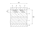
- 2 is a cross-sectional view taken along the line AA in FIG. 1.
- 2 is a cross-sectional view taken along the line BB in FIG. 1.
- 3A to 3C are cross-sectional views illustrating steps in a method for manufacturing the silicon carbide semiconductor device according to the first embodiment.
- 5A to 5C are cross-sectional views illustrating steps corresponding to FIG. 2 and continuing from FIG. 4 in the method for manufacturing the silicon carbide semiconductor device according to the first embodiment.
- 5A to 5C are cross-sectional views illustrating steps corresponding to FIG. 3 and subsequent to FIG. 4 in the method for manufacturing the silicon carbide semiconductor device according to the first embodiment.
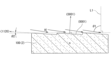
- 1 is a cross-sectional view showing a case where ions are implanted at an angle toward an off-angle side of a semiconductor substrate.
- 11 is another cross-sectional view showing the case where ions are implanted at an angle opposite to the off-angle of the semiconductor substrate.
- 1 is a cross-sectional view of a silicon carbide semiconductor device according to a first comparative example.
- FIG. 11 is a cross-sectional view of a silicon carbide semiconductor device according to a second comparative example.
- 11 is a graph showing a simulation result of an impurity profile by ion implantation from a vertical direction when acceleration energy is changed.
- 11 is a graph showing a simulation result of an impurity profile by ion implantation from an oblique direction when the acceleration energy is changed.
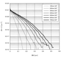
- FIG. 11 is a graph showing a simulation result of an impurity profile by ion implantation when the implantation angle is changed.
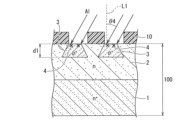
- FIG. 11 is a cross-sectional view of a silicon carbide semiconductor device according to a second embodiment.
- 7A to 7C are cross-sectional views illustrating steps in a method for manufacturing a silicon carbide semiconductor device according to a second embodiment.
- FIG. 11 is a cross-sectional view of a silicon carbide semiconductor device according to a third embodiment.
- 11A to 11C are cross-sectional views illustrating steps in a method for manufacturing a silicon carbide semiconductor device according to a third embodiment.
- FIG. 11 is a cross-sectional view of a silicon carbide semiconductor device according to a fourth embodiment.
- FIG. 10A to 10C are cross-sectional views illustrating steps in a method for manufacturing a silicon carbide semiconductor device according to a fourth embodiment. 19 in the method for manufacturing the silicon carbide semiconductor device according to the fourth embodiment.
- FIG. 21A to 21C are cross-sectional views illustrating a process subsequent to FIG. 20 in the method for manufacturing the silicon carbide semiconductor device according to the fourth embodiment.
- 21 through 24 are cross-sectional views illustrating a process subsequent to FIG. 21 in the method for manufacturing the silicon carbide semiconductor device according to the fourth embodiment.
- 23A to 23C are cross-sectional views illustrating a process subsequent to FIG. 22 in the method for manufacturing the silicon carbide semiconductor device according to the fourth embodiment.
- 24A to 24C are cross-sectional views illustrating a process subsequent to FIG.
- 25A to 25C are cross-sectional views illustrating a process subsequent to FIG. 24 in the method for manufacturing the silicon carbide semiconductor device according to the fourth embodiment.
- 26A to 26C are cross-sectional views illustrating a process subsequent to FIG. 25 in the method for manufacturing the silicon carbide semiconductor device according to the fourth embodiment.
- 27A to 27C are cross-sectional views illustrating a process subsequent to FIG. 26 in the method for manufacturing the silicon carbide semiconductor device according to the fourth embodiment.
- 27 through 31 are cross-sectional views illustrating a process subsequent to FIG. 27 in the method for manufacturing the silicon carbide semiconductor device according to the fourth embodiment. 29 is a cross-sectional view showing a process subsequent to FIG.
- FIG. 13 is a cross-sectional view of a silicon carbide semiconductor device according to a fifth embodiment.
- FIG. 13 is a cross-sectional view of a silicon carbide semiconductor device according to a sixth embodiment.
- the first to sixth embodiments of the present disclosure will be described with reference to the drawings.
- identical or similar parts will be given the same or similar reference numerals, and duplicate descriptions will be omitted.
- the drawings are schematic, and the relationship between thickness and planar dimensions, the ratio of thickness of each layer, etc. may differ from the actual ones.
- the drawings may include parts with different dimensional relationships and ratios.
- the first to sixth embodiments shown below are examples of devices and methods for embodying the technical ideas of the present disclosure, and the technical ideas of the present disclosure do not specify the materials, shapes, structures, arrangements, etc. of the components as described below.
- the source region of a metal oxide semiconductor field effect transistor is "one main region (first main region)” that can be selected as an emitter region in an insulated gate bipolar transistor (IGBT) and as a cathode region in a thyristor such as a MOS-controlled static induction thyristor (SI thyristor) or a diode.
- the drain region of a MOSFET is "the other main region (second main region)” that can be selected as a collector region in an IGBT and as an anode region in a thyristor or a diode.
- main region when the term “main region” is used simply, it means either “one main region (first main region)” or “the other main region (second main region)” that is appropriate from the technical common sense of a person skilled in the art.
- the first conductivity type is n-type and the second conductivity type is p-type.
- the conductivity types may be selected in the opposite relationship, with the first conductivity type being p-type and the second conductivity type being n-type.
- a "+” or “-” attached to "n” or “p” means that the semiconductor region has a relatively high or low impurity concentration, respectively, compared to a semiconductor region without a "+” or "-” attached.
- the impurity concentrations of the respective semiconductor regions are strictly the same.
- SiC crystals also have crystal polymorphism, the main ones being the cubic 3C structure (3C-SiC), as well as the hexagonal 4H structure (4H-SiC) and 6H structure (6H-SiC).
- the band gap at room temperature has been reported to be 2.23 eV for 3C-SiC, 3.26 eV for 4H-SiC, and 3.02 eV for 6H-SiC. This disclosure will exemplify the case where 4H-SiC and 3C-SiC are primarily used.
- a diode having a merged PN Schottky (MPS) structure is exemplified as the silicon carbide semiconductor device according to the first embodiment.
- the MPS structure is a structure in which a Schottky junction and a pn junction are mixed on the upper surface side of a semiconductor substrate.
- FIG. 1 is a plan view of a silicon carbide semiconductor device according to the first embodiment.
- the silicon carbide semiconductor device according to the first embodiment comprises an active region 101 provided in a semiconductor substrate (semiconductor base) 100, and a termination region 102 provided in the semiconductor substrate 100 so as to surround the periphery of the active region 101.
- the active region 101 is a region through which current flows when the diode is in the on state.
- the termination region 102 is a region that relieves the electric field applied to the end of the active region 101 and maintains a breakdown voltage.
- anode regions 3 which are a plurality of semiconductor layers of a second conductivity type (p + type), are provided on the upper surface side of the drift layer 2, which is a semiconductor layer of a first conductivity type (n type).
- the anode regions 3 In a planar pattern, the anode regions 3 have linear (striped) portions extending parallel to each other in one direction (the vertical direction in FIG. 1).
- the anode regions 3 are arranged apart from each other in a direction (the horizontal direction in FIG. 1) perpendicular to the extension direction of the anode regions 3.
- the number of the anode regions 3 arranged is not particularly limited.
- Fig. 2 shows a cross-sectional view taken along a direction perpendicular to the extension direction of the anode region 3, as viewed from the AA direction in Fig. 1.
- a cathode region 1 of a first conductivity type (n + type) is provided on the lower surface side of a semiconductor substrate 100.
- the cathode region 1 is formed of a substrate (SiC substrate) made of SiC, such as 4H-SiC.
- a drift layer 2 of a first conductivity type (n-type) having a lower impurity concentration than the cathode region 1 is provided on the upper surface side of the cathode region 1.
- the drift layer 2 is composed of an epitaxially grown layer made of SiC, such as 4H-SiC.
- An n-type buffer layer may be provided between the cathode region 1 and the drift layer 2.
- the impurity concentration of the n-type buffer layer may be lower than the impurity concentration of the cathode region 1 and higher than the impurity concentration of the drift layer 2.
- a plurality of p + type anode regions 3 are provided at a distance from each other on the upper surface side of the drift layer 2.
- Each of the p + type anode regions 3 forms a pn junction with the n type drift layer 2.
- the anode regions 3 are formed by ion implantation of p type impurities such as aluminum (Al) or boron (B) into the drift layer 2.
- the anode region 3 When viewed from the A-A direction in FIG. 1, the anode region 3 has a substantially rectangular cross-sectional shape in a cross-sectional view along a direction perpendicular to the extension direction of the planar pattern of the anode region 3.
- FIG. 3 shows a cross-sectional view along the extension direction of the anode region 3 as seen from the B-B direction in FIG. 1.
- the anode region 3 in a cross-sectional view along the extension direction of the planar pattern of the anode region 3, the anode region 3 has a cross-sectional shape of an approximately parallelogram.
- the upper and lower surfaces of the anode region 3 are approximately parallel, and both inclined side surfaces of the anode region 3 are approximately parallel.
- the angle ⁇ 0 between the normal L1 to the upper surface of the semiconductor substrate 100 and the inclined side surface of the anode region 3 is, for example, about 30° or more and less than 90°.
- the anode region 3 is formed to have a cross-sectional shape of an approximately parallelogram by ion implanting p-type impurities from an oblique direction inclined with respect to the normal L1 to the upper surface of the semiconductor substrate 100.
- the side surface of the anode region 3 is approximately parallel to the injection direction of the ions.
- a p-type electric field relaxation layer is provided on the upper surface side of the drift layer 2. If this electric field relaxation layer contacts or overlaps the end of the anode region 3, the anode region 3 does not need to have a cross-sectional shape that is approximately a parallelogram.
- the depth d1 of the anode region 3 is, for example, about 0.1 ⁇ m or more and 0.5 ⁇ m or less, and may be about 0.1 ⁇ m or more and 0.3 ⁇ m or less.
- the depth d1 of the anode region 3 may be about 0.5 ⁇ m or more. The greater the inclination angle of the ion implantation to form the anode region 3 with respect to the normal L1 of the upper surface of the semiconductor substrate 100, the shallower the depth d1 of the anode region 3.
- the impurity concentration in the range from the upper surface of the anode region 3 to a depth of 0.3 ⁇ m is, for example, about 1 ⁇ 10 18 /cm 3 or more and 1 ⁇ 10 22 /cm 3 or less, and it is preferable to be about 1 ⁇ 10 19 /cm 3 or more and 1 ⁇ 10 22 /cm 3 or less because it has a lower resistance.
- the impurity concentration in the upper surface of the anode region 3 may be about 1 ⁇ 10 20 /cm 3 or more and 1 ⁇ 10 22 /cm 3 or less.
- the impurity concentration in the range from the upper surface of the anode region 3 to a depth of about 0.3 ⁇ m may be uniform, and the impurity concentration in the range from the upper surface of the anode region 3 to a depth of about 0.4 ⁇ m may be uniform.
- "Uniform impurity concentration" includes not only the case where the impurity concentration is strictly the same, but also the range in which the impurity concentration varies within ⁇ 10%.
- the impurity concentration in a range 0.5 ⁇ m or more away from the top surface of the anode region 3 is lower than the impurity concentration in a range 0.3 ⁇ m deep from the top surface of the anode region 3.
- the impurity concentration in the range 0.5 ⁇ m or more away from the top surface of the anode region 3 is, for example, about 1 ⁇ 10 17 /cm 3 or less.
- the proportion of 3C-SiC contained in the surface layer of the anode region 3 is, for example, about 10% or more and 100% or less.
- the surface layer of the anode region 3 may be a mixed crystal of 3C-SiC and 4H-SiC.
- the surface layer of the anode region 3 may also contain an amorphous structure, 4H-SiC, etc. Since 3C-SiC has a narrower band gap than 4H-SiC, the surface layer of the anode region 3 containing 3C-SiC can make ohmic contact with the anode electrode 5 on the upper surface side of the anode region 3 with low resistance.
- the lower part (lower part) of the surface layer of the anode region 3 may be composed of 4H-SiC.
- the area ratio of the crystal structure on the surface can be measured using a field emission scanning electron microscope (FE-SEM) and electron backscatter diffraction (EBSD).
- FE-SEM field emission scanning electron microscope
- EBSD electron backscatter diffraction
- an anode electrode (upper electrode) 5 is provided on the upper surface side of the drift layer 2 and the anode region 3. Note that the anode electrode 5 is not shown in Figure 1.
- the anode electrode 5 is in contact with the upper surfaces of the drift layer 2 and the anode region 3.
- the anode electrode 5 is made of a metal such as aluminum (Al), an Al alloy, or molybdenum (Mo). Examples of Al alloys include Al-silicon (Si), Al-copper (Cu), and Al-Si-Cu.
- the anode electrode 5 may have a barrier metal layer in the portion in contact with the anode region 3.
- the barrier metal layer may be made of a metal such as titanium nitride (TiN), titanium (Ti), or a TiN/Ti laminate structure with Ti as the lower layer.
- the metal material of the portion of the anode electrode 5 in contact with the anode region 3 is, for example, aluminum (Al), an Al alloy, molybdenum (Mo), titanium (Ti), or titanium nitride (TiN).
- the anode region 3 Since the surface layer of the anode region 3 contains 3C-SiC, the anode region 3 is in ohmic contact with the anode electrode 5 with low resistance. For this reason, no silicide layer made of nickel silicide (NiSi) or the like is provided between the anode electrode 5 and the anode region 3. On the other hand, the drift layer 2 sandwiched between adjacent anode regions 3 forms a Schottky junction with the anode electrode 5.
- NiSi nickel silicide
- the silicon carbide semiconductor device has an MPS structure that combines pn junctions between multiple anode regions 3 and the drift layer 2, and Schottky junctions between the drift layer 2 between the anode regions 3 and the anode electrode 5. This makes it possible to reduce the electric field strength at the junction between the semiconductor substrate 100 and the anode electrode 5, thereby suppressing reverse leakage current.
- a cathode electrode (back electrode) 6 is provided on the underside of the cathode region 1.
- the cathode electrode 6 is composed of a single layer film made of a metal such as gold (Au), or a laminated film in which titanium (Ti), nickel (Ni), and gold (Au) are laminated in this order.
- a silicide layer may also be provided between the cathode region 1 and the cathode electrode 6.
- a starting substrate which is a first conductivity type (n + type) SiC substrate made of SiC such as 4H-SiC and doped with n-type impurities such as nitrogen (N)
- the upper surface of the cathode region 1 may have an off angle of, for example, about 0° to 8° (for example, about 4°).
- a first conductivity type (n type) drift layer 2 made of SiC such as 4H-SiC and doped with n-type impurities such as N is epitaxially grown on the cathode region 1.
- the upper surface of the cathode region 1 has an off angle
- the upper surface of the drift layer 2 also has a similar off angle.
- the cathode region 1 and the drift layer 2 constitute a semiconductor substrate 100.
- a photoresist film 7 (see FIG. 5 ) is applied to the upper surface of the drift layer 2, and the photoresist film 7 is patterned using a photolithography technique.
- p-type impurities such as aluminum (Al) are ion-implanted into the upper surface of the drift layer 2, as shown in FIG. 5 , to form a p + type anode region 3 on the upper surface side of the drift layer 2.
- FIG. 6 shows a cross section corresponding to FIG. 3 during the ion implantation shown in FIG. 5.
- p-type impurities are ion-implanted obliquely at a predetermined angle ⁇ 1 with respect to the normal L1 to the upper surface of the semiconductor substrate 100.
- the predetermined angle ⁇ 1 is, for example, about 30° or more and less than 90°, or may be about 45° or more and less than 90°, or may be about 60° or more and less than 90°.
- the larger the predetermined angle ⁇ 1 the shallower the anode region 3 is formed.
- FIG. 6 by tilting the injection direction of ion implantation in the longitudinal direction (extension direction) of the planar pattern of the anode region 3, shadowing (misalignment between the mask and ion implantation) can be prevented.
- the acceleration energy of the ion implantation is about 300 keV or more and 700 keV or less, and may be about 400 keV or more and 700 keV or less.
- damage 4 can be introduced into the surface layer of the anode region 3, as shown diagrammatically by "x" in Figures 5 and 6, and the crystal structure of the 4H-SiC can be destroyed to form an amorphous structure.
- the off angle ⁇ 2 is the angle between the top surface of the semiconductor substrate 100 (shown by the dashed line) and a plane (basal plane) perpendicular to the c-axis, which is the (0001) plane (silicon (Si) plane) or the (000-1) plane (carbon (C) plane).
- the predetermined angle ⁇ 1 is set to approximately less than (90°- ⁇ 2), which is less than the angle parallel to the off angle direction. This makes it possible to prevent the injection direction from becoming parallel to the off angle ⁇ 2, and allows the ion injection to be performed uniformly.
- the injection angle ⁇ 1 may be set to approximately less than 86°.
- the predetermined angle ⁇ 1 with respect to the normal L1 to the top surface of the semiconductor substrate 100 can be set to less than about 90°, allowing the ion implantation to be performed uniformly.
- FIG. 8 illustrates an example in which the injection direction of ion implantation is tilted in a direction opposite to the off angle direction. In this case, the injection angle ⁇ 1 can be set to less than about 90°.
- the implanted p-type impurities are activated by heat treatment (activation annealing) at a temperature of, for example, 1600°C or higher and 1900°C or lower.
- heat treatment activation annealing
- the amorphous structure of the surface layer of the anode region 3 is recrystallized to become 3C-SiC.
- an anode electrode 5 made of aluminum (Al) or the like is formed on the upper surface side of the drift layer 2 and the anode region 3 by sputtering or vapor deposition (see Figures 2 and 3).
- the drift layer 2 and the anode electrode 5 form a Schottky junction, and the anode region 3 and the anode electrode 5 form an ohmic contact with low resistance.
- the semiconductor substrate 100 is ground from the underside to adjust the thickness of the semiconductor substrate 100 to the product thickness.
- a cathode electrode 6 made of gold (Au) or the like is formed on the entire underside of the semiconductor substrate 100 by sputtering or vapor deposition (see Figures 2 and 3). Thereafter, the semiconductor substrate 100 is cut (diced) into individual pieces to complete the silicon carbide semiconductor device according to the first embodiment.
- a silicon carbide semiconductor device according to a first comparative example will be described.
- the silicon carbide semiconductor device according to the first comparative example is different from the silicon carbide semiconductor device according to the first embodiment shown in FIG. 2 in that a silicide layer 8 made of nickel silicide (NiSi) is provided between the p + type anode region 3 and the anode electrode 5.
- the depth d2 of the anode region 3 is the same as the depth d1 of the anode region 3 of the silicon carbide semiconductor device according to the first embodiment shown in FIG. 2.
- the anode region 3 is made of 4H-SiC, and the silicide layer 8 is provided between the anode region 3 and the anode electrode 5 in order to make ohmic contact between the anode region 3 and the anode electrode 5.
- p-type impurities are ion-implanted from the normal direction to the upper surface of the semiconductor substrate 100 without being tilted relative to the normal to the upper surface of the semiconductor substrate 100.
- the acceleration energy during ion implantation is less than 300 keV, which is lower than the acceleration energy during ion implantation in the method for manufacturing a silicon carbide semiconductor device according to the first embodiment.
- a metal film such as nickel (Ni) is formed on the upper surface side of the anode region 3, and heat treatment is performed to form a silicide layer 8.
- the silicon carbide semiconductor device and manufacturing method thereof in the ion implantation step for forming the anode region 3, p-type impurities are ion-implanted into the upper surface of the drift layer 2 from an oblique direction inclined at a predetermined angle ⁇ 1 with respect to the normal L1 to the upper surface of the semiconductor substrate 100.
- the anode region 3 can be formed shallowly despite the high acceleration energy, and damage 4 can be introduced into the surface layer of the anode region 3 to form 3C-SiC, so that the anode region 3 and the anode electrode 5 can be in ohmic contact with low resistance.
- the silicon carbide semiconductor device according to the second comparative example differs from the silicon carbide semiconductor device according to the first embodiment in that the depth d3 of the p + type anode region 3 is deeper than the depth d1 of the anode region 3 shown in FIG. 2.
- the surface layer of the anode region 3 contains damage 4 caused by ion implantation for forming the anode region 3 and contains 3C-SiC. Therefore, the anode region 3 and the anode electrode 5 are in ohmic contact with each other with low resistance, and no silicide layer is provided between the anode region 3 and the anode electrode 5.
- p-type impurities are ion-implanted from the normal direction to the upper surface of the semiconductor substrate 100 without being tilted relative to the normal to the upper surface of the semiconductor substrate 100.
- the acceleration energy during ion implantation is 300 keV or more, which is similar to the acceleration energy during ion implantation in the method for manufacturing a silicon carbide semiconductor device according to the first embodiment, so that damage 4 occurs in the surface layer of the anode region 3, and 3C-SiC is formed in the surface layer of the anode region 3 after heat treatment.
- ions are implanted at high acceleration from the normal direction of the upper surface of the semiconductor substrate 100, so that the p-type impurity is implanted at a deep position, lowering the impurity concentration in the surface layer of the anode region 3.
- p-type impurities are ion-implanted into the upper surface of the drift layer 2 from an oblique direction inclined at a predetermined angle ⁇ 1 with respect to the normal L1 to the upper surface of the semiconductor substrate 100.
- This makes it possible to increase the impurity concentration in the surface layer of the anode region 3 while causing damage 4 on the upper surface side of the anode region 3. This makes it possible to reduce the process load.
- ⁇ Simulation results> 11 shows the results of a Monte Carlo simulation of impurity profiles when phosphorus (P) or aluminum (Al) is ion-implanted from the normal direction of the upper surface of the wafer, and the acceleration energy of the ion implantation is changed to 30 keV, 100 keV, 200 keV, 500 keV, 1000 keV, 1500 keV, and 2000 keV.
- the horizontal axis of FIG. 11 indicates the depth from the upper surface of the wafer, and the vertical axis of FIG. 11 indicates the impurity concentration (damage). As shown in FIG. 11, it can be seen that the higher the acceleration energy, the deeper the damage is.
- FIG. 12 shows the results of a Monte Carlo simulation of the impurity profile when the ion species is Al, the wafer off-angle is 4°, the dose is 1 ⁇ 10 13 cm -2 , the implantation angle with respect to the normal direction of the upper surface of the wafer is fixed at 86°, and the implantation energy is changed to 100 keV, 200 keV, 300 keV, 400 keV, 500 keV, 600 keV, and 700 keV.
- the horizontal axis of FIG. 12 indicates the depth from the upper surface of the wafer, and the vertical axis of FIG. 12 indicates the impurity concentration (damage).
- a high-concentration damage layer with an impurity concentration of 1 ⁇ 10 20 cm -3 or more needs to be at least 0.1 ⁇ m deep from the top surface of the wafer.
- the reason for this is that a portion of the wafer at a depth of about 0.1 ⁇ m from the top surface may disappear due to a subsequent oxidation process. Therefore, it is preferable that the acceleration energy is 400 keV or more, which results in a depth of about 1 ⁇ 10 20 cm -3 at a depth of about 0.1 ⁇ m from the top surface of the wafer.
- FIG. 13 shows the results of a Monte Carlo simulation of the impurity profile when the ion species is Al, the wafer off-angle is 4°, the dose is 1 ⁇ 10 13 cm -2 , the implantation energy is fixed at 300 keV, and the implantation angle with respect to the normal direction to the top surface of the wafer is changed to 0°, 15°, 30°, 45°, 60°, 75°, and 86°.
- the horizontal axis of Fig. 13 indicates the depth from the top surface of the wafer, and the vertical axis of Fig. 13 indicates the impurity concentration (damage).
- the peak damage amount is similar when the implantation angle is 0° and 15°.
- the implantation angle is 30° or more, the amount of damage increases and 3C-SiC increases. Therefore, it is preferable that the implantation angle with respect to the normal direction of the top surface of the wafer is 30° or more.
- Second Embodiment 14 shows a cross section of the silicon carbide semiconductor device according to the second embodiment when viewed from the A-A direction in FIG. 1.
- the silicon carbide semiconductor device according to the second embodiment is different from the silicon carbide semiconductor device according to the first embodiment in that the anode region 3 has a substantially parallelogram cross-sectional shape in a cross-sectional view along a direction perpendicular to the extension direction of the planar pattern of the anode region 3.
- the anode region 3 has a substantially rectangular cross-sectional shape in a cross-sectional view along the extension direction of the planar pattern of the anode region 3 when viewed from the B-B direction in FIG. 1.
- Other configurations of the silicon carbide semiconductor device according to the second embodiment are similar to those of the silicon carbide semiconductor device according to the first embodiment, so that repeated explanations will be omitted.
- the method for manufacturing a silicon carbide semiconductor device according to the second embodiment involves patterning a photoresist film 9 in a cross-sectional view taken along a direction perpendicular to the extension direction of the planar pattern of the anode region 3, and then using the patterned photoresist film 9 as an ion implantation mask to ion-implant p-type impurities from an oblique direction inclined at an angle ⁇ 3 with respect to the normal L1 to the top surface of the semiconductor substrate 100, thereby forming the anode region 3.
- the other steps of the method for manufacturing a silicon carbide semiconductor device according to the second embodiment are the same as those of the method for manufacturing a silicon carbide semiconductor device according to the first embodiment.
- p-type impurities are ion-implanted into the upper surface of the drift layer 2 from an oblique direction inclined at a predetermined angle ⁇ 3 with respect to the normal L1 to the upper surface of the semiconductor substrate 100.
- This causes damage 4 in the surface layer of the anode region 3, forming 3C-SiC, allowing ohmic contact between the anode region 3 and the anode electrode 5, eliminating the need for a silicide layer.
- the impurity concentration in the surface layer of the anode region 3 can be increased, reducing the process load.
- Third Embodiment 16 shows a cross section of the silicon carbide semiconductor device according to the third embodiment when viewed from the A-A direction in FIG. 1.
- the silicon carbide semiconductor device according to the third embodiment is different from the silicon carbide semiconductor device according to the first embodiment in that the anode region 3 has a substantially trapezoidal cross-sectional shape in a cross-sectional view along a direction perpendicular to the extension direction of the planar pattern of the anode region 3.
- the anode region 3 has a substantially rectangular cross-sectional shape in a cross-sectional view along the extension direction of the planar pattern of the anode region 3 when viewed from the B-B direction in FIG. 1.
- Other configurations of the silicon carbide semiconductor device according to the third embodiment are similar to those of the silicon carbide semiconductor device according to the first embodiment, so that repeated explanations will be omitted.
- ion implantation is performed twice to form the anode region 3.
- the photoresist film 9 is patterned, and the patterned photoresist film 9 is used as an ion implantation mask to implant p-type impurities from an oblique direction inclined at an angle ⁇ 3 with respect to the normal L1 to the upper surface of the semiconductor substrate 100.
- the photoresist film 9 is then removed.
- the photoresist film 10 is patterned, and the patterned photoresist film 10 is used as an ion implantation mask to implant p-type impurities from an oblique direction inclined at an angle ⁇ 4, which is the same angle as the angle ⁇ 3 shown in FIG. 15, in the opposite direction to the normal line L1 of the upper surface of the semiconductor substrate 100. Then, the photoresist film 10 is removed.
- the ion implantation for forming the anode region 3 is performed twice, the dose amount for each time is changed to be smaller than when the ion implantation for forming the anode region 3 is performed once.
- the other steps of the method for manufacturing a silicon carbide semiconductor device according to the third embodiment are the same as those of the method for manufacturing a silicon carbide semiconductor device according to the first embodiment.
- p-type impurities are ion-implanted into the upper surface of the drift layer 2 from an oblique direction inclined at a predetermined angle ⁇ 3, ⁇ 4 with respect to the normal L1 to the upper surface of the semiconductor substrate 100.
- This causes damage 4 in the surface layer of the anode region 3, forming 3C-SiC, allowing ohmic contact between the anode region 3 and the anode electrode 5, eliminating the need for a silicide layer.
- the impurity concentration in the surface layer of the anode region 3 can be increased, reducing the process load.
- the anode region 3 can be formed with a substantially trapezoidal cross-sectional shape, thereby improving left-right symmetry.
- the silicon carbide semiconductor device according to the fourth embodiment includes a drift layer 12 which is a semiconductor layer of a first conductivity type (n - type).
- the drift layer 12 is formed of an epitaxially grown layer made of SiC, such as 4H-SiC.
- a current spreading layer (CSL) 13 which is an n + type semiconductor layer having a higher impurity density than the drift layer 12, is provided on the upper surface side of the drift layer 12.
- the current spreading layer 13 is formed of an epitaxially grown layer made of SiC such as 4H-SiC.
- the current spreading layer 13 may be a region in which n-type impurities are ion-implanted in the upper part of the drift layer 12. Note that the current spreading layer 13 is not necessarily required, and when the current spreading layer 13 is not provided, the drift layer 2 may be provided up to the region of the current spreading layer 13.
- Base regions 17a to 17c which are semiconductor layers of the second conductivity type (p-type), are provided on the upper surface side of the current diffusion layer 13.
- the base regions 17a to 17c are composed of epitaxially grown layers made of SiC, such as 4H-SiC.
- the base regions 17a to 17c may be regions in which p-type impurities are ion-implanted into the current diffusion layer 13.
- first main electrode regions (source regions) 18a to 18d which are n + type semiconductor layers having a higher impurity density than the drift layer 12.
- the source regions 18a to 18d are formed by ion implantation of n type impurities such as nitrogen (N), phosphorus (P) or arsenic (As) from a direction oblique to the normal to the upper surface of the base regions 17a to 17c.
- the depth of the source regions 18a to 18d may be, for example, about 0.1 ⁇ m or more and 0.5 ⁇ m or less, and may be about 0.1 ⁇ m or more and 0.3 ⁇ m or less.
- the depth of the source regions 18a to 18d may be about 0.5 ⁇ m or more.
- the impurity concentration in the range from the top surface of the source regions 18a to 18d to a depth of 0.3 ⁇ m is, for example, about 1 ⁇ 10 18 /cm 3 or more and 1 ⁇ 10 22 /cm 3 or less, and is preferably about 1 ⁇ 10 19 /cm 3 or more and 1 ⁇ 10 22 /cm 3 or less because it provides a lower resistance.
- the impurity concentration of the top surface of the source regions 18a to 18d may be about 1 ⁇ 10 20 /cm 3 or more and 1 ⁇ 10 22 /cm 3 or less.
- the impurity concentration may be uniform within a range from the upper surfaces of the source regions 18a to 18d to a depth of 0.3 ⁇ m.
- the impurity concentration in a range 0.5 ⁇ m or more away from the top surfaces of the source regions 18a to 18d is lower than the impurity concentration in a range 0.3 ⁇ m or more away from the top surfaces of the source regions 18a to 18d.
- the impurity concentration in the range 0.5 ⁇ m or more away from the top surfaces of the source regions 18a to 18d is, for example, about 1 ⁇ 10 17 /cm 3 or less.
- the source regions 18a to 18d are mainly composed of 4H-SiC.
- damage occurs to at least the upper surface (surface layer) of the source regions 18a to 18d, destroying the crystal structure of the 4H-SiC and forming an amorphous structure.
- Subsequent heat treatment (activation annealing) recrystallizes the amorphous structure to form 3C-SiC. For this reason, the surface layers of the source regions 18a to 18d contain 3C-SiC.
- the proportion of 3C-SiC contained in the surface layers of the source regions 18a to 18d is, for example, about 10% or more and 100% or less.
- the surface layers of the source regions 18a to 18d may be a mixed crystal of 3C-SiC and 4H-SiC.
- the surface layers of the source regions 18a to 18d may contain amorphous structures, 4H-SiC, etc., in addition to 3C-SiC.
- Base contact regions 19a to 19c which are p + type semiconductor layers having a higher impurity density than the base regions 17a to 17c, are provided on the upper surface sides of the base regions 17a to 17c so as to contact the source regions 18a to 18d.
- the base contact regions 19a to 19c have a substantially trapezoidal cross-sectional shape.
- the base contact regions 19a to 19c are formed by ion implantation of p-type impurities such as aluminum (Al) or boron (B) from an oblique direction relative to the normal to the upper surfaces of the base regions 17a to 17c.
- the depth of the base contact regions 19a to 19c is, for example, about 0.1 ⁇ m or more and 0.5 ⁇ m or less, and may be about 0.1 ⁇ m or more and 0.3 ⁇ m or less.
- the depth of the base contact regions 19a to 19c may be about 0.5 ⁇ m or more.
- the impurity concentration in the range from the upper surface of the base contact regions 19a to 19c to a depth of 0.3 ⁇ m is, for example, about 1 ⁇ 10 18 /cm 3 or more and 1 ⁇ 10 22 /cm 3 or less, and is preferably about 1 ⁇ 10 19 /cm 3 or more and 1 ⁇ 10 22 /cm 3 or less because it provides a lower resistance.
- the impurity concentration of the upper surface of the base contact regions 19a to 19c may be about 1 ⁇ 10 20 /cm 3 or more and 1 ⁇ 10 22 /cm 3 or less.
- the impurity concentration may be uniform within a range from the upper surfaces of the base contact regions 19a to 19c to a depth of 0.3 ⁇ m.
- the impurity concentration in a range 0.5 ⁇ m or more away from the upper surfaces of the base contact regions 19a to 19c is lower than the impurity concentration in a range 0.3 ⁇ m or more away from the upper surfaces of the base contact regions 19a to 19c.
- the impurity concentration in the range 0.5 ⁇ m or more away from the upper surfaces of the base contact regions 19a to 19c is, for example, about 1 ⁇ 10 17 /cm 3 or less.
- the base contact regions 19a to 19c are mainly composed of 4H-SiC.
- damage occurs to at least the upper surface (surface layer) of the base contact regions 19a to 19c, destroying the crystal structure of the 4H-SiC and forming an amorphous structure.
- Subsequent heat treatment (activation annealing) recrystallizes the amorphous structure to form 3C-SiC. For this reason, the surface layer of the base contact regions 19a to 19c contains 3C-SiC.
- the proportion of 3C-SiC contained in the surface layer of the base contact regions 19a to 19c is, for example, about 10% or more and 100% or less.
- the surface layer of the base contact regions 19a to 19c may be a mixed crystal of 3C-SiC and 4H-SiC.
- the surface layer of the base contact regions 19a to 19c may contain an amorphous structure, 4H-SiC, etc., in addition to 3C-SiC.
- Trenches 31a and 31b are provided, which are dug in the depth direction from the upper surface side of the source regions 18a to 18d.
- the trenches 31a and 31b penetrate the source regions 18a to 18d and the base regions 17a to 17c and reach the current spreading layer 13.
- the trenches 31a and 31b may have a planar pattern extending in a stripe shape in the depth direction and forward direction of the paper surface of FIG. 18, or may have a dot-shaped planar pattern.
- Gate insulating films 20a and 20b are provided on the bottom and side surfaces of the trenches 31a and 31b. Gate electrodes 21a and 21b are embedded inside the trenches 31a and 31b via the gate insulating films 20a and 20b.
- SiO2 film silicon oxide film
- SiON silicon oxynitride
- SrO strontium oxide
- Si3N4 silicon nitride
- Al2O3 aluminum oxide
- MgO magnesium oxide
- the material of the gate electrodes 21a and 21b for example, a polysilicon layer (doped polysilicon layer) to which p-type impurities or n-type impurities are added at a high impurity concentration, or a high melting point metal such as titanium (Ti), tungsten (W), or nickel (Ni) can be used.
- a polysilicon layer doped polysilicon layer to which p-type impurities or n-type impurities are added at a high impurity concentration
- a high melting point metal such as titanium (Ti), tungsten (W), or nickel (Ni)
- p + -type gate bottom protection regions 14a, 14b are provided in contact with the bottoms of the trenches 31a, 31b.
- the base bottom buried region (15a, 16a) includes a first buried region 15a and a second buried region 16a provided on the upper surface of the first buried region 15a.
- the base bottom buried region (15b, 16b) includes a first buried region 15b and a second buried region 16b provided on the upper surface of the first buried region 15b.
- the base bottom buried region (15c, 16c) includes a first buried region 15c and a second buried region 16c provided on the upper surface of the first buried region 15c.
- a first main electrode (source electrode) (24, 25, 26) is provided on the upper surface side of the gate electrodes 21a, 21b via interlayer insulating films 22a, 22b.
- interlayer insulating films 22a, 22b a silicon oxide film ( SiO2 film) not containing impurities, called an "NSG film", a silicon oxide film (PSG film) doped with phosphorus, a silicon oxide film (BSG film) doped with boron, etc. can be used.
- interlayer insulating films 22a, 22b a single layer film of a silicon oxide film (BPSG film) or a silicon nitride film ( Si3N4 film) doped with phosphorus and boron, or a composite film in which a plurality of types of these are selected and combined can also be used.
- BPSG film silicon oxide film
- Si3N4 film silicon nitride film
- composite film in which a plurality of types of these are selected and combined can also be used.
- the source electrodes (24, 25, 26) are in ohmic contact with the source regions 18a-18d and the base contact regions 19a-19c with low resistance.
- the source electrodes (24, 25, 26) include a first barrier metal layer 24, a second barrier metal layer 25, and a wiring layer 26.
- the first barrier metal layer 24 is in contact with the base contact regions 19a-19c and the source regions 18a-18d.
- the second barrier metal layer 25 is provided so as to cover the first barrier metal layer 24.
- the wiring layer 26 is provided so as to cover the second barrier metal layer 25.
- the first barrier metal layer 24 is made of titanium nitride (TiN)
- the second barrier metal layer 25 is made of titanium (Ti)/TiN/Ti
- the wiring layer 26 is made of aluminum (Al).
- the metal material of the portions of the source electrodes (24, 25, 26) that contact the base contact regions 19a-19c and the source regions 18a-18d is, for example, aluminum (Al), an Al alloy, molybdenum (Mo), titanium (Ti), or titanium nitride (TiN).
- n + type second main electrode region (drain region) 11 having a higher impurity concentration than the drift layer 12 is provided on the lower surface side of the drift layer 12.
- the drain region 11 is configured of a substrate (SiC substrate) made of SiC such as 4H—SiC.
- a second main electrode (drain electrode) 27 is disposed on the underside of the drift layer 12 so as to contact the drift layer 12.
- the drain electrode 27 may be, for example, a single layer film made of gold (Au) or a metal film laminated in the order of Al, nickel (Ni), and Au, and may further include a metal plate of molybdenum (Mo), tungsten (W), or the like laminated on the bottom layer.
- a positive voltage is applied to the drain electrode 27, and a positive voltage equal to or greater than the threshold is applied to the gate electrodes 21a and 21b, forming an inversion layer (channel) on the gate electrodes 21a and 21b side of the base regions 17a to 17c, resulting in an ON state.
- a current flows from the drain electrode 27 to the source electrodes (24, 25, 26) via the drain region 11, drift layer 12, the inversion layer in the base regions 17a to 17c, and the source regions 18a to 18d.
- an n + type semiconductor substrate made of SiC such as 4H-SiC and doped with n-type impurities such as nitrogen (N) is prepared.
- the upper surface of the SiC substrate may have an off angle of about 4°.
- an n- type drift layer 12 made of SiC such as 4H-SiC is epitaxially grown on the upper surface of the drain region 11, as shown in FIG.
- n-type impurity ions such as nitrogen (N) are implanted into the entire surface of the drift layer 12 from the upper surface side of the drift layer 12 to form an n + type current diffusion layer 13 made of SiC such as 4H-SiC, as shown in Fig. 20.
- the current diffusion layer 13 may be epitaxially grown on the upper surface of the drift layer 12.
- the current diffusion layer 13 is not necessarily formed, and the following process may be performed on the drift layer 12.
- first buried regions 15a-15c and gate bottom protection regions 14a, 14b are formed inside the current diffusion layer 13 by photolithography and ion implantation. Furthermore, second buried regions 16a-16c are formed on the upper surface side of the first buried regions 15a-15c above the current diffusion layer 13 by photolithography and ion implantation.
- a p-type base region 17 made of SiC such as 4H-SiC is epitaxially grown on the top surface of the current spreading layer 13.
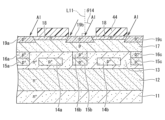
- an ion implantation process for forming an n + type source region 18 is performed in two steps.
- a photoresist film 41 (see FIG. 23) is applied onto the base region 17, and the photoresist film 41 is patterned using a photolithography technique.
- n-type impurities such as N are ion-implanted from an oblique direction inclined at a predetermined angle ⁇ 11 with respect to the normal line L11 of the upper surface of the base region 17.
- an n + type source region 18 is formed having a cross-sectional shape of an approximately parallelogram.
- the photoresist film 41 is removed. Note that an oxide film may be used as a mask instead of the photoresist film 41.
- the predetermined angle ⁇ 11 is, for example, about 30° or more and less than 90°, may be about 45° or more and less than 90°, or may be about 60° or more and less than 90°.
- the acceleration energy of the ion implantation is about 300 keV or more and 700 keV or less, or may be about 400 keV or more and 700 keV or less.
- a photoresist film 42 (see FIG. 24) is applied onto the base region 17, and the photoresist film 42 is patterned using photolithography.
- n-type impurities such as N are ion-implanted from an oblique direction inclined at an angle ⁇ 12 that is the same as the predetermined angle ⁇ 11 on the opposite side of the first ion implantation step with respect to the normal line L11 of the upper surface of the base region 17.
- the predetermined angle ⁇ 12 is, for example, about 30° or more and less than 90°, may be about 45° or more and less than 90°, or may be about 60° or more and less than 90°.
- the acceleration energy of the ion implantation is about 300 keV or more and 700 keV or less, or may be about 400 keV or more and 700 keV or less.
- ion implantation for forming p + type base contact regions 19a to 19c is performed in two steps.
- a photoresist film 43 (see FIG. 25) is applied onto the base region 17, and the photoresist film 43 is patterned using photolithography.
- p-type impurity ions such as Al are implanted from an oblique direction inclined at a predetermined angle ⁇ 13 with respect to the normal line L11 of the upper surface of the base region 17.
- p + type base contact regions 19a to 19c are formed on the upper surface side of the base region 17 with a cross-sectional shape of a substantially parallelogram.
- the photoresist film 43 is removed. Note that an oxide film may be used as a mask instead of the photoresist film 43.
- the predetermined angle ⁇ 13 is, for example, about 30° or more and less than 90°, may be about 45° or more and less than 90°, or may be about 60° or more and less than 90°.
- the acceleration energy of the ion implantation is about 300 keV or more and 700 keV or less, and may be about 400 keV or more and 700 keV or less.
- a photoresist film 44 (see FIG. 26) is applied onto the base region 17, and the photoresist film 44 is patterned using photolithography.
- p-type impurity ions such as Al are implanted from an oblique direction inclined at an angle ⁇ 14, which is the same as the predetermined angle ⁇ 13, on the opposite side of the first ion implantation step with respect to the normal line L11 of the upper surface of the base region 17, as shown in FIG. 26.
- the predetermined angle ⁇ 14 is, for example, about 30° or more and less than 90°, may be about 45° or more and less than 90°, or may be about 60° or more and less than 90°.
- the acceleration energy of the ion implantation is about 300 keV or more and 700 keV or less, and may be about 400 keV or more and 700 keV or less.
- the n-type impurity ions and p-type impurity ions implanted by each ion implantation are activated by heat treatment (activation annealing) at a temperature of, for example, 1600°C or higher and 1900°C or lower.
- heat treatment activation annealing
- the amorphous structure of the surface layers of the source region 18 and base contact regions 19a to 19c is recrystallized to become 3C-SiC.
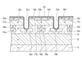
- a photoresist film 45 (see FIG. 27) is applied onto the source region 18 and the base contact regions 19a-19c, and the photoresist film 45 is patterned using photolithography.
- the patterned photoresist film 45 as an etching mask, trenches 31a, 31b are selectively formed by dry etching such as reactive ion etching (RIE) to penetrate the source regions 18a-18d and base regions 17a-17c and reach the current diffusion layer 13, as shown in FIG. 27.
- RIE reactive ion etching
- the photoresist film 45 is then removed. Note that an oxide film may be used as a mask instead of the photoresist film 45.
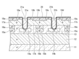
- a gate insulating film 20 is formed on the bottom and side surfaces of the trenches 31a and 31b and on the top surfaces of the source region 18 and the p + type base contact regions 19a to 19c by thermal oxidation, CVD, or the like.
- a polysilicon layer doped polysilicon layer to which impurities such as N are added at a high concentration is deposited on the gate insulating film 20 by CVD, or the like.
- the polysilicon layer is embedded inside the trenches 31a and 31b via the gate insulating film 20, thereby forming the gate electrodes 21a and 21b.
- an interlayer insulating film is deposited on the gate electrodes 21a, 21b and the gate insulating film 20 by CVD or the like.
- a photoresist film 46 (see FIG. 30) is applied onto the interlayer insulating film, and the photoresist film 46 is patterned using photolithography techniques.
- the patterned photoresist film 46 as an etching mask, as shown in FIG. 30, a portion of the interlayer insulating films 22a, 22b and the gate insulating film 20 is selectively removed by dry etching to open contact holes. Thereafter, the photoresist film 46 is removed.
- a first barrier metal layer 24 and a second barrier metal layer 25 are formed by sputtering, vapor deposition, or the like, as shown in FIG. 31.
- the wiring layer 26 shown in FIG. 18 is formed by sputtering, vapor deposition, or the like.
- the source electrode (24, 25, 26) is formed by the first barrier metal layer 24, the second barrier metal layer 25, and the wiring layer 26.
- the drain electrode 27 shown in FIG. 18 is formed on the entire lower surface of the drain region 11 by sputtering, vapor deposition, or the like. In this manner, the silicon carbide semiconductor device according to the fourth embodiment is completed.
- ion implantation may be performed in only one of the ion implantation steps for forming the base contact regions 19a-19c and for forming the source region 18, with an implantation direction at an angle of 30° or more and less than 90° to the normal L11 to the top surface of the base region 17, and with an acceleration energy of 300 keV or more.
- only one of the base contact regions 19a-19c and the source regions 18a-18d shown in FIG. 18 may contain 3C-SiC and be in ohmic contact with the source electrode (24, 25, 26) with low resistance.
- the ion implantation process for forming the n + type source region 18 may not be performed twice, and only one of the first and second ion implantation processes may be performed. Furthermore, when only one of the first and second ion implantation processes is performed, n-type impurities such as N may be ion-implanted from an oblique direction onto the entire upper surface of the base region 17 without using the photoresist films 41 and 42. In that case, the source region 18 is formed over the entire upper part of the base region 17.
- ions may be implanted with an acceleration energy of less than 300 keV from the direction of the normal line L11 of the upper surface of the base region 17.
- the base contact regions 19a to 19c instead of performing the ion implantation process to form the base contact regions 19a to 19c in two separate steps, only one of the first and second ion implantation processes may be performed.
- the base contact regions 19a to 19c have a cross-sectional shape that is approximately a parallelogram.
- n-type impurities are ion-implanted into the upper surface of the base region 17 from an oblique direction inclined by a predetermined angle ⁇ 11, ⁇ 12 with respect to the normal L11 of the upper surface of the base region 17.
- the source region 18 can be formed shallowly despite the high acceleration energy, and 3C-SiC can be formed by damaging the surface layer of the source region 18, so that the source region 18 and the source electrode (24, 25, 26) can be in ohmic contact with low resistance.
- the impurity concentration in the surface layer of the base contact regions 19a to 19c can be increased while damage is applied to the upper surface side of the base contact regions 19a to 19c, thereby reducing the process load.
- the silicon carbide semiconductor device according to the fifth embodiment differs from the silicon carbide semiconductor device according to the fourth embodiment shown in Fig. 18 in that base contact regions 19a-19c have a substantially parallelogram cross-sectional shape.
- Other configurations of the silicon carbide semiconductor device according to the fifth embodiment are similar to those of the silicon carbide semiconductor device according to the fourth embodiment, and therefore repeated description will be omitted.
- the method for manufacturing a silicon carbide semiconductor device according to the fifth embodiment differs from the method for manufacturing a silicon carbide semiconductor device according to the fourth embodiment in that the ion implantation for forming the base contact regions 19a to 19c is not divided into two steps, but only the first ion implantation step shown in FIG. 25 is performed, and the second ion implantation step shown in FIG. 26 is not performed.
- the silicon carbide semiconductor device and manufacturing method thereof according to the fifth embodiment provide the same effects as the silicon carbide semiconductor device and manufacturing method thereof according to the fourth embodiment.
- the silicon carbide semiconductor device according to the sixth embodiment differs from the silicon carbide semiconductor device according to the fourth embodiment shown in Fig. 18 in that base contact regions 19a-19c have a substantially rectangular cross-sectional shape.
- Other configurations of the silicon carbide semiconductor device according to the sixth embodiment are similar to those of the silicon carbide semiconductor device according to the fourth embodiment, and therefore repeated description will be omitted.
- the method for manufacturing a silicon carbide semiconductor device according to the sixth embodiment differs from the method for manufacturing a silicon carbide semiconductor device according to the fourth embodiment in that, in the two ion implantation steps for forming the base contact regions 19a to 19c, the implantation direction is tilted toward the front and back of FIG. 33.
- the silicon carbide semiconductor device and manufacturing method thereof according to the sixth embodiment achieves the same effects as the silicon carbide semiconductor device and manufacturing method thereof according to the fourth embodiment.
- a MOSFET is exemplified, but the present invention can also be applied to an IGBT.
- the n + type source regions 18a to 18d of the MOSFET shown in FIG. 18 may be used as emitter regions, and a p + type collector region may be provided instead of the n + type drain region 11.
- the present invention can also be applied to a reverse conducting IGBT (RC-IGBT) or a reverse blocking insulated gate bipolar transistor (RB-IGBT).
- RC-IGBT reverse conducting IGBT
- RB-IGBT reverse blocking insulated gate bipolar transistor
- a MOSFET having a trench gate structure is exemplified, but the present invention can also be applied to a MOSFET or IGBT having a planar gate structure.
Landscapes
- Electrodes Of Semiconductors (AREA)
- Chemical & Material Sciences (AREA)
- Crystallography & Structural Chemistry (AREA)
Priority Applications (4)
| Application Number | Priority Date | Filing Date | Title |
|---|---|---|---|
| JP2025535614A JPWO2025022836A1 (https=) | 2023-07-24 | 2024-06-06 | |
| CN202480006266.9A CN120457789A (zh) | 2023-07-24 | 2024-06-06 | 碳化硅半导体装置及其制造方法 |
| DE112024000247.1T DE112024000247T5 (de) | 2023-07-24 | 2024-06-06 | Siliziumcarbid-halbleitervorrichtung und verfahren zu ihrer herstellung |
| US19/249,293 US20250324741A1 (en) | 2023-07-24 | 2025-06-25 | Silicon carbide semiconductor device and method of manufacturing the same |
Applications Claiming Priority (2)
| Application Number | Priority Date | Filing Date | Title |
|---|---|---|---|
| JP2023119859 | 2023-07-24 | ||
| JP2023-119859 | 2023-07-24 |
Related Child Applications (1)
| Application Number | Title | Priority Date | Filing Date |
|---|---|---|---|
| US19/249,293 Continuation US20250324741A1 (en) | 2023-07-24 | 2025-06-25 | Silicon carbide semiconductor device and method of manufacturing the same |
Publications (1)
| Publication Number | Publication Date |
|---|---|
| WO2025022836A1 true WO2025022836A1 (ja) | 2025-01-30 |
Family
ID=94374761
Family Applications (1)
| Application Number | Title | Priority Date | Filing Date |
|---|---|---|---|
| PCT/JP2024/020731 Pending WO2025022836A1 (ja) | 2023-07-24 | 2024-06-06 | 炭化珪素半導体装置及びその製造方法 |
Country Status (5)
| Country | Link |
|---|---|
| US (1) | US20250324741A1 (https=) |
| JP (1) | JPWO2025022836A1 (https=) |
| CN (1) | CN120457789A (https=) |
| DE (1) | DE112024000247T5 (https=) |
| WO (1) | WO2025022836A1 (https=) |
Citations (14)
| Publication number | Priority date | Publication date | Assignee | Title |
|---|---|---|---|---|
| JP2004282091A (ja) * | 2000-06-27 | 2004-10-07 | Matsushita Electric Ind Co Ltd | 半導体デバイス |
| WO2008056698A1 (en) * | 2006-11-10 | 2008-05-15 | Sumitomo Electric Industries, Ltd. | Silicon carbide semiconductor device and process for producing the same |
| JP2009049198A (ja) * | 2007-08-20 | 2009-03-05 | New Japan Radio Co Ltd | 半導体装置およびその製造方法 |
| JP2009152309A (ja) * | 2007-12-19 | 2009-07-09 | Toyota Motor Corp | 半導体装置及び半導体装置の製造方法 |
| JP2011165902A (ja) * | 2010-02-10 | 2011-08-25 | Toshiba Corp | 半導体装置および半導体装置の製造方法 |
| JP2013232559A (ja) * | 2012-04-27 | 2013-11-14 | National Institute Of Advanced Industrial & Technology | 炭化珪素半導体装置の製造方法 |
| JP2018101789A (ja) * | 2018-01-25 | 2018-06-28 | 株式会社日立製作所 | 半導体スイッチング素子および炭化珪素半導体装置の製造方法 |
| JP2018190994A (ja) * | 2018-07-10 | 2018-11-29 | 株式会社東芝 | 半導体装置 |
| JP2019021761A (ja) * | 2017-07-18 | 2019-02-07 | 株式会社 日立パワーデバイス | 半導体装置およびその製造方法 |
| WO2019107411A1 (ja) * | 2017-11-29 | 2019-06-06 | 国立研究開発法人科学技術振興機構 | トンネル電界効果トランジスタ |
| JP2020136479A (ja) * | 2019-02-19 | 2020-08-31 | パナソニックIpマネジメント株式会社 | 半導体素子 |
| JP2021150503A (ja) * | 2020-03-19 | 2021-09-27 | 株式会社東芝 | 半導体装置、半導体装置の製造方法、インバータ回路、駆動装置、車両、及び、昇降機 |
| WO2022163082A1 (ja) * | 2021-02-01 | 2022-08-04 | ローム株式会社 | SiC半導体装置 |
| US20230024105A1 (en) * | 2021-07-21 | 2023-01-26 | Infineon Technologies Ag | Method of manufacturing ohmic contacts on a silicon carbide (sic) substrate, method of manufacturing a semiconductor device, and semiconductor device |
-
2024
- 2024-06-06 CN CN202480006266.9A patent/CN120457789A/zh active Pending
- 2024-06-06 JP JP2025535614A patent/JPWO2025022836A1/ja active Pending
- 2024-06-06 WO PCT/JP2024/020731 patent/WO2025022836A1/ja active Pending
- 2024-06-06 DE DE112024000247.1T patent/DE112024000247T5/de active Pending
-
2025
- 2025-06-25 US US19/249,293 patent/US20250324741A1/en active Pending
Patent Citations (14)
| Publication number | Priority date | Publication date | Assignee | Title |
|---|---|---|---|---|
| JP2004282091A (ja) * | 2000-06-27 | 2004-10-07 | Matsushita Electric Ind Co Ltd | 半導体デバイス |
| WO2008056698A1 (en) * | 2006-11-10 | 2008-05-15 | Sumitomo Electric Industries, Ltd. | Silicon carbide semiconductor device and process for producing the same |
| JP2009049198A (ja) * | 2007-08-20 | 2009-03-05 | New Japan Radio Co Ltd | 半導体装置およびその製造方法 |
| JP2009152309A (ja) * | 2007-12-19 | 2009-07-09 | Toyota Motor Corp | 半導体装置及び半導体装置の製造方法 |
| JP2011165902A (ja) * | 2010-02-10 | 2011-08-25 | Toshiba Corp | 半導体装置および半導体装置の製造方法 |
| JP2013232559A (ja) * | 2012-04-27 | 2013-11-14 | National Institute Of Advanced Industrial & Technology | 炭化珪素半導体装置の製造方法 |
| JP2019021761A (ja) * | 2017-07-18 | 2019-02-07 | 株式会社 日立パワーデバイス | 半導体装置およびその製造方法 |
| WO2019107411A1 (ja) * | 2017-11-29 | 2019-06-06 | 国立研究開発法人科学技術振興機構 | トンネル電界効果トランジスタ |
| JP2018101789A (ja) * | 2018-01-25 | 2018-06-28 | 株式会社日立製作所 | 半導体スイッチング素子および炭化珪素半導体装置の製造方法 |
| JP2018190994A (ja) * | 2018-07-10 | 2018-11-29 | 株式会社東芝 | 半導体装置 |
| JP2020136479A (ja) * | 2019-02-19 | 2020-08-31 | パナソニックIpマネジメント株式会社 | 半導体素子 |
| JP2021150503A (ja) * | 2020-03-19 | 2021-09-27 | 株式会社東芝 | 半導体装置、半導体装置の製造方法、インバータ回路、駆動装置、車両、及び、昇降機 |
| WO2022163082A1 (ja) * | 2021-02-01 | 2022-08-04 | ローム株式会社 | SiC半導体装置 |
| US20230024105A1 (en) * | 2021-07-21 | 2023-01-26 | Infineon Technologies Ag | Method of manufacturing ohmic contacts on a silicon carbide (sic) substrate, method of manufacturing a semiconductor device, and semiconductor device |
Also Published As
| Publication number | Publication date |
|---|---|
| US20250324741A1 (en) | 2025-10-16 |
| DE112024000247T5 (de) | 2025-10-23 |
| JPWO2025022836A1 (https=) | 2025-01-30 |
| CN120457789A (zh) | 2025-08-08 |
Similar Documents
| Publication | Publication Date | Title |
|---|---|---|
| US10777677B2 (en) | Insulated gate semiconductor device and method of manufacturing same | |
| JP7643621B2 (ja) | 半導体装置 | |
| JP6988175B2 (ja) | 炭化珪素半導体装置および炭化珪素半導体装置の製造方法 | |
| JP6705155B2 (ja) | 半導体装置および半導体装置の製造方法 | |
| JP2019102737A (ja) | 半導体装置及びその製造方法 | |
| JP6802454B2 (ja) | 半導体装置およびその製造方法 | |
| JP7823679B2 (ja) | 炭化珪素半導体装置 | |
| JP7703882B2 (ja) | 炭化珪素半導体装置及びその製造方法 | |
| JP7622449B2 (ja) | 半導体装置 | |
| JP2018060923A (ja) | 半導体装置および半導体装置の製造方法 | |
| JP6508369B2 (ja) | 炭化珪素半導体装置およびその製造方法 | |
| JP7782643B2 (ja) | 炭化珪素半導体装置の製造方法 | |
| JP2021093522A (ja) | 炭化珪素半導体装置および炭化珪素半導体装置の製造方法 | |
| JP2019003966A (ja) | 炭化珪素半導体装置および炭化珪素半導体装置の製造方法 | |
| JP7231040B2 (ja) | 炭化珪素半導体装置および炭化珪素半導体装置の製造方法 | |
| US20230282709A1 (en) | Silicon carbide semiconductor device and silicon carbide semiconductor substrate | |
| JP2017092364A (ja) | 半導体装置および半導体装置の製造方法 | |
| JP2022106161A (ja) | 半導体装置 | |
| WO2025022836A1 (ja) | 炭化珪素半導体装置及びその製造方法 | |
| JP2024148334A (ja) | 炭化珪素半導体装置及びその製造方法 | |
| JP2024125067A (ja) | 炭化珪素半導体装置及びその製造方法 | |
| JP2021068741A (ja) | 半導体装置 | |
| JP2024133974A (ja) | 炭化珪素半導体装置 | |
| JP2025088287A (ja) | 炭化珪素半導体装置の製造方法及び炭化珪素半導体装置 | |
| JP2024141950A (ja) | 炭化珪素半導体装置及びその製造方法 |
Legal Events
| Date | Code | Title | Description |
|---|---|---|---|
| WWE | Wipo information: entry into national phase |
Ref document number: 202480006266.9 Country of ref document: CN Ref document number: 112024000247 Country of ref document: DE |
|
| ENP | Entry into the national phase |
Ref document number: 2025535614 Country of ref document: JP Kind code of ref document: A |
|
| WWE | Wipo information: entry into national phase |
Ref document number: 2025535614 Country of ref document: JP |
|
| WWP | Wipo information: published in national office |
Ref document number: 202480006266.9 Country of ref document: CN |
|
| WWP | Wipo information: published in national office |
Ref document number: 112024000247 Country of ref document: DE |