WO2025018232A1 - 調光デバイス用エレクトロクロミック素子、調光デバイス用エレクトロクロミック素子の製造方法、透明電極層、及び、透明電極層の製造方法 - Google Patents
調光デバイス用エレクトロクロミック素子、調光デバイス用エレクトロクロミック素子の製造方法、透明電極層、及び、透明電極層の製造方法 Download PDFInfo
- Publication number
- WO2025018232A1 WO2025018232A1 PCT/JP2024/024824 JP2024024824W WO2025018232A1 WO 2025018232 A1 WO2025018232 A1 WO 2025018232A1 JP 2024024824 W JP2024024824 W JP 2024024824W WO 2025018232 A1 WO2025018232 A1 WO 2025018232A1
- Authority
- WO
- WIPO (PCT)
- Prior art keywords
- transparent electrode
- electrode layer
- oxide
- light
- layer
- Prior art date
- Legal status (The legal status is an assumption and is not a legal conclusion. Google has not performed a legal analysis and makes no representation as to the accuracy of the status listed.)
- Ceased
Links
Images





Classifications
-
- G—PHYSICS
- G02—OPTICS
- G02F—OPTICAL DEVICES OR ARRANGEMENTS FOR THE CONTROL OF LIGHT BY MODIFICATION OF THE OPTICAL PROPERTIES OF THE MEDIA OF THE ELEMENTS INVOLVED THEREIN; NON-LINEAR OPTICS; FREQUENCY-CHANGING OF LIGHT; OPTICAL LOGIC ELEMENTS; OPTICAL ANALOGUE/DIGITAL CONVERTERS
- G02F1/00—Devices or arrangements for the control of the intensity, colour, phase, polarisation or direction of light arriving from an independent light source, e.g. switching, gating or modulating; Non-linear optics
- G02F1/01—Devices or arrangements for the control of the intensity, colour, phase, polarisation or direction of light arriving from an independent light source, e.g. switching, gating or modulating; Non-linear optics for the control of the intensity, phase, polarisation or colour
- G02F1/15—Devices or arrangements for the control of the intensity, colour, phase, polarisation or direction of light arriving from an independent light source, e.g. switching, gating or modulating; Non-linear optics for the control of the intensity, phase, polarisation or colour based on an electrochromic effect
-
- G—PHYSICS
- G02—OPTICS
- G02F—OPTICAL DEVICES OR ARRANGEMENTS FOR THE CONTROL OF LIGHT BY MODIFICATION OF THE OPTICAL PROPERTIES OF THE MEDIA OF THE ELEMENTS INVOLVED THEREIN; NON-LINEAR OPTICS; FREQUENCY-CHANGING OF LIGHT; OPTICAL LOGIC ELEMENTS; OPTICAL ANALOGUE/DIGITAL CONVERTERS
- G02F1/00—Devices or arrangements for the control of the intensity, colour, phase, polarisation or direction of light arriving from an independent light source, e.g. switching, gating or modulating; Non-linear optics
- G02F1/01—Devices or arrangements for the control of the intensity, colour, phase, polarisation or direction of light arriving from an independent light source, e.g. switching, gating or modulating; Non-linear optics for the control of the intensity, phase, polarisation or colour
- G02F1/15—Devices or arrangements for the control of the intensity, colour, phase, polarisation or direction of light arriving from an independent light source, e.g. switching, gating or modulating; Non-linear optics for the control of the intensity, phase, polarisation or colour based on an electrochromic effect
- G02F1/1514—Devices or arrangements for the control of the intensity, colour, phase, polarisation or direction of light arriving from an independent light source, e.g. switching, gating or modulating; Non-linear optics for the control of the intensity, phase, polarisation or colour based on an electrochromic effect characterised by the electrochromic material, e.g. by the electrodeposited material
- G02F1/1523—Devices or arrangements for the control of the intensity, colour, phase, polarisation or direction of light arriving from an independent light source, e.g. switching, gating or modulating; Non-linear optics for the control of the intensity, phase, polarisation or colour based on an electrochromic effect characterised by the electrochromic material, e.g. by the electrodeposited material comprising inorganic material
-
- G—PHYSICS
- G02—OPTICS
- G02F—OPTICAL DEVICES OR ARRANGEMENTS FOR THE CONTROL OF LIGHT BY MODIFICATION OF THE OPTICAL PROPERTIES OF THE MEDIA OF THE ELEMENTS INVOLVED THEREIN; NON-LINEAR OPTICS; FREQUENCY-CHANGING OF LIGHT; OPTICAL LOGIC ELEMENTS; OPTICAL ANALOGUE/DIGITAL CONVERTERS
- G02F1/00—Devices or arrangements for the control of the intensity, colour, phase, polarisation or direction of light arriving from an independent light source, e.g. switching, gating or modulating; Non-linear optics
- G02F1/01—Devices or arrangements for the control of the intensity, colour, phase, polarisation or direction of light arriving from an independent light source, e.g. switching, gating or modulating; Non-linear optics for the control of the intensity, phase, polarisation or colour
- G02F1/15—Devices or arrangements for the control of the intensity, colour, phase, polarisation or direction of light arriving from an independent light source, e.g. switching, gating or modulating; Non-linear optics for the control of the intensity, phase, polarisation or colour based on an electrochromic effect
- G02F1/1514—Devices or arrangements for the control of the intensity, colour, phase, polarisation or direction of light arriving from an independent light source, e.g. switching, gating or modulating; Non-linear optics for the control of the intensity, phase, polarisation or colour based on an electrochromic effect characterised by the electrochromic material, e.g. by the electrodeposited material
- G02F1/1523—Devices or arrangements for the control of the intensity, colour, phase, polarisation or direction of light arriving from an independent light source, e.g. switching, gating or modulating; Non-linear optics for the control of the intensity, phase, polarisation or colour based on an electrochromic effect characterised by the electrochromic material, e.g. by the electrodeposited material comprising inorganic material
- G02F1/1524—Transition metal compounds
-
- G—PHYSICS
- G02—OPTICS
- G02F—OPTICAL DEVICES OR ARRANGEMENTS FOR THE CONTROL OF LIGHT BY MODIFICATION OF THE OPTICAL PROPERTIES OF THE MEDIA OF THE ELEMENTS INVOLVED THEREIN; NON-LINEAR OPTICS; FREQUENCY-CHANGING OF LIGHT; OPTICAL LOGIC ELEMENTS; OPTICAL ANALOGUE/DIGITAL CONVERTERS
- G02F1/00—Devices or arrangements for the control of the intensity, colour, phase, polarisation or direction of light arriving from an independent light source, e.g. switching, gating or modulating; Non-linear optics
- G02F1/01—Devices or arrangements for the control of the intensity, colour, phase, polarisation or direction of light arriving from an independent light source, e.g. switching, gating or modulating; Non-linear optics for the control of the intensity, phase, polarisation or colour
- G02F1/15—Devices or arrangements for the control of the intensity, colour, phase, polarisation or direction of light arriving from an independent light source, e.g. switching, gating or modulating; Non-linear optics for the control of the intensity, phase, polarisation or colour based on an electrochromic effect
- G02F1/153—Constructional details
- G02F1/155—Electrodes
Definitions
- the present invention relates to an electrochromic element for a light-adjusting device that changes color through an electrochemical reaction and a method for manufacturing the same, and in particular to an electrochromic element for a light-adjusting device that provides a high-contrast color change in the near-infrared band (wavelengths of 800 to 2500 nm) and a method for manufacturing the same.
- the present invention also relates to a transparent electrode layer used in such an electrochromic element for a light-adjusting device and a method for manufacturing the transparent electrode layer.
- ITO indium tin oxide
- ITO is an n-type degenerate semiconductor
- the electrons which are carriers, contribute to electrical conduction.
- these carrier electrons reflect and absorb light of a certain wavelength or more.
- the carrier density is about 1 ⁇ 10 21 cm ⁇ 3 and the resistivity is very low at 2 ⁇ 10 ⁇ 4 ⁇ cm, so infrared rays of 1000 nm or more are absorbed or reflected and hardly transmitted.
- Patent Document 1 discloses an electrochromic element that can greatly change the transmittance not only in the visible light region but also in the infrared light region by controlling the carrier electron density of a transparent electrode (conductive film). It is said that by controlling the carrier electron density of at least one of the two opposing transparent electrodes to a low value of 1 to 4 ⁇ 10 20 cm -3 in consideration of the balance with the response speed of the transmittance control, it is possible to greatly change not only the transmittance in the visible light region but also the transmittance in the infrared light region.
- the film thickness should be increased to increase the conductivity of the transparent electrode.
- transparent electrodes such as ITO result in a lower transmittance in the near-infrared band.
- the resistivity of a material is defined as 1/(Ne ⁇ ), where ⁇ is mobility, and is inversely proportional to the product of the carrier electron density N and the mobility ⁇ . Therefore, as described in Patent Document 1, if the carrier electron density is lowered to increase the transmittance in the infrared region, the resistivity increases, making it difficult to respond quickly to dimming.
- the present invention was made in consideration of the above-mentioned circumstances, and its purpose is to provide an electrochromic element for a light control device that provides a color change in the near-infrared to mid-infrared band (wavelengths 800 to 4000 nm), and in particular a high-contrast color change in the near-infrared band (wavelengths 800 to 2500 nm), a method for manufacturing the same, a transparent electrode layer, and a method for manufacturing the transparent electrode layer.
- the inventors of the present application have considered using known zinc oxide-based transparent electrode layers, such as aluminum-doped zinc oxide and gallium-doped zinc oxide, instead of ITO, but the adhesion to the electrochromic layer is low and sufficient functionality cannot be achieved.
- a transparent electrode film with high carrier mobility and high solar transmittance can be obtained by forming a precursor film made of indium oxide containing more amorphous phase or amorphous phase components than polycrystalline components, and then crystallizing the precursor film by irradiating the precursor film with light at a temperature of 100°C or less or by heat treatment at a temperature of more than 150°C in the atmosphere or in a vacuum.
- Such a transparent electrode film is chemically stable when combined with an electrochromic layer made of a transition metal oxide and an electrochromic layer containing a metal cyano complex, and provides an electrochromic element that stably exhibits color changes in the mid-infrared band (wavelengths of 800 to 4000 nm) and also stably exhibits color changes with high contrast in the near-infrared band (wavelengths of 800 to 2500 nm).
- the transparent electrode layer can be polycrystallized by light irradiation, it is possible to use a low heat-resistant substrate that has flexibility like a resin sheet but is limited in its ability to withstand heating, enabling versatile development of various electrochromic elements according to needs.
- the present invention provides an electrochromic element for a light-adjusting device, the electrochromic element having a multilayer structure including a first electrochromic layer, an electrolyte layer, and a second electrochromic layer, in this order, between a first transparent electrode layer on a first transparent substrate and a second transparent electrode layer on a second transparent substrate,
- the first transparent electrode layer and the second transparent electrode layer contain at least one of an oxide of indium (In) and an oxide of indium (In) containing one or more elements selected from the group consisting of Ce, W, Ti, Zr, and Mo, and are characterized by having a carrier mobility of 70 cm 2 /V ⁇ s or more and a transmittance of 75% or more in the near-infrared band (800 to 2500 nm).
- the first transparent electrode layer and the second transparent electrode layer may be characterized in that they are made of a crystalline phase obtained by crystallizing an amorphous phase. This characteristic makes it possible to provide an electrochromic element for a light control device that provides a color change in the mid-infrared band and a stable color change with high contrast in the near-infrared band.
- the first transparent substrate and the second transparent substrate may be resin sheets. This feature makes it possible to provide a flexible electrochromic element for a light control device.
- the electrolyte layer may contain at least one of bis(trifluoromethanesulfonyl)imide, lithium bis(trifluoromethanesulfonyl)imide, potassium bis(trifluoromethanesulfonyl)imide, and sodium bis(trifluoromethanesulfonyl)imide, as well as at least one organic solvent selected from propylene carbonate, ethylene carbonate, and diethyl carbonate, and may be solidified with at least one of acrylic resin and epoxy resin, the first electrochromic layer may contain a transition metal oxide, and the second electrochromic layer may contain a metal cyano complex, and may be characterized in that a color change is possible by applying a voltage to the first transparent electrode layer and the second transparent electrode layer.
- the transition metal oxide may be characterized by including at least one of tungsten oxide, molybdenum oxide, niobium oxide, vanadium oxide, and titanium oxide.
- the metal cyano complex is represented by the formula A x M[M'(CN) 6 ] y.zH 2 , where A is a cation selected from the group consisting of hydrogen, lithium, sodium, potassium, rubidium, cesium, and ammonium; M is a metal atom selected from the group consisting of vanadium, chromium, manganese, iron, ruthenium, cobalt, rhodium, nickel, palladium, platinum, copper, silver, zinc, lanthanum, europium, gadolinium, lutetium, barium, strontium, and calcium; M' is a metal atom selected from the group consisting of vanadium, chromium, molybdenum, tungsten, manganese, iron, ruthenium, cobalt, nickel, platinum, and copper ; x is a rational number from 0 to 3; y is a rational number from 0.3 to 1.5; and z is
- the present invention provides a transparent electrode layer used in an electrochromic element for a light-adjusting device, the transparent electrode layer being formed on a transparent substrate, containing at least one of an oxide of indium (In) alone and an oxide of indium (In) containing one or more elements selected from the group consisting of Ce, W, Ti, Zr, and Mo, and having a carrier mobility of 70 cm 2 /V ⁇ s or more and a transmittance of 75% or more in the near-infrared band (800 to 2500 nm).
- an electrochromic element for a light-adjusting device can be provided that imparts a color change in the mid-infrared band and a high-contrast color change in the near-infrared band.
- the present invention provides a method for producing an electrochromic element for a light-adjusting device having a multilayer structure including a first electrochromic layer, an electrolyte layer, and a second electrochromic layer in this order between a first transparent electrode layer on a first transparent substrate and a second transparent electrode layer on a second transparent substrate, the method comprising: forming the first transparent electrode layer on the first transparent substrate and/or forming the second transparent electrode layer on the second transparent substrate; the electrode forming step comprises: a first step of forming, on the first transparent substrate and/or the second transparent substrate, a precursor film including an amorphous phase including at least one of an oxide of indium (In) and an oxide of indium (In) including one or more selected from the group consisting of Ce, W, Ti, Zr, and Mo; and a second step of crystallizing the precursor film to form the first transparent electrode layer and/or the second transparent electrode layer having a carrier mobility of 70 cm 2 /V ⁇ s or more and a transmittance of 75% or more
- the second step is characterized by including a step of irradiating light.
- the crystallization process may be characterized as being a process in which treatment is performed at a temperature of 100°C or less.
- the first transparent substrate and the second transparent substrate may be resin sheets.
- the electrolyte layer may contain at least one of bis(trifluoromethanesulfonyl)imide, lithium bis(trifluoromethanesulfonyl)imide, potassium bis(trifluoromethanesulfonyl)imide, and sodium bis(trifluoromethanesulfonyl)imide, as well as at least one organic solvent selected from propylene carbonate, ethylene carbonate, and diethyl carbonate, and may be solidified with at least one of acrylic resin and epoxy resin, the first electrochromic layer may contain a transition metal oxide, the second electrochromic layer may contain a metal cyano complex, and the electrochromic element for the light control device may be characterized in that it is capable of changing color by applying a voltage to the first transparent electrode layer and the second transparent electrode layer.
- the invention may further include a photoaging process of irradiating the multilayer structure with light after the multilayer structure is formed.
- a method for producing a transparent electrode layer used in an electrochromic element for a light control device comprising: an electrode forming step of forming a transparent electrode layer on a transparent substrate, the electrode forming step comprising: a first step of forming, on the transparent substrate, a precursor film having an amorphous phase containing at least one of an oxide of indium (In) and an oxide of indium (In) containing one or more elements selected from the group consisting of Ce, W, Ti, Zr, and Mo; and a second step of crystallizing the precursor film to form the transparent electrode layer having a carrier mobility of 70 cm 2 /V ⁇ s or more and a transmittance of 75% or more in the near-infrared band (800 to 2500 nm).
- FIG. 1 is a cross-sectional view showing an electrochromic element according to the present invention.
- 1A and 1B are diagrams showing the transmission spectrum and the reflection spectrum of each transparent electrode layer, respectively.
- 1 is a list of the surface roughness of each transparent electrode layer.
- FIG. 13 is a graph showing the water contact angle for each transparent electrode layer after each treatment.
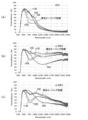
- FIG. 13 shows the optical spectra when a WO3 thin film (multilayer film A) or a PB thin film (multilayer film B) is provided to each transparent electrode layer, and when no thin film is provided (only the substrate).
- 1 is a table summarizing spectroscopic properties.
- FIG. 1 shows (a) cyclic voltammogram of ECD, and (b) time course of transmittance for the color change reaction.
- FIG. 1 shows (a) the electrochemical characteristics by chronocoulometry of ECD, and (b) the transmittance change.
- FIG. 1 is a diagram showing optical spectral changes in transmittance and reflectance during the bleaching and coloring reactions of an ECD. 1 is a table summarizing the spectroscopic properties of ECD.
- FIG. 1 is a diagram showing the time-dependent characteristics of the optical spectrum change (transmittance in the bleached state) of an ECD.
- FIG. 1 is a diagram showing the optical characteristics (transmittance in a bleached state) of an ECD in the mid-infrared band measured by Fourier transform infrared spectroscopy.
- ECD electrochromic device
- the electrochromic device (EC) 1 has a multi-layer structure using a transition metal oxide and a metal cyano complex as an electrochromic material (EC material). That is, it includes a first electrochromic (EC) layer 12a containing a transition metal oxide, a second electrochromic (EC) layer 12b containing a metal cyano complex, an electrolyte layer 10 sandwiched between them, and a first transparent electrode layer 14a and a second transparent electrode layer 14b mainly composed of indium oxide ( In2O3 ) connected to the first EC layer 12a and the second EC layer 12b from the outside, respectively.
- In2O3 indium oxide
- a first transparent substrate 16a and a second transparent substrate 16b made of a transparent material such as resin or glass are provided on the outside of the first transparent electrode layer 14a and the second transparent electrode layer 14b, respectively. That is, the first transparent substrate 16a, the first transparent electrode layer 14a, the first EC layer 12a, the electrolyte layer 10, the second EC layer 12b, the second transparent electrode layer 14b, and the second transparent substrate 16b are laminated in this order.
- transparent electrode layers when it is not necessary to distinguish between the first transparent electrode layer 14a and the second transparent electrode layer 14b, they are referred to as transparent electrode layers, and when it is not necessary to distinguish between the first transparent substrate 16a and the second transparent substrate 16b, they are referred to as transparent substrates.
- the electrochromic element for the light-adjusting device has a multilayer structure including, in this order, a first electrochromic layer, an electrolyte layer, and a second electrochromic layer between the first transparent electrode layer on the first transparent substrate and the second transparent electrode layer on the second transparent substrate.
- the electrolyte layer 10, the first EC layer 12a and the second EC layer 12b to be combined with the first transparent electrode layer 14a and the second transparent electrode layer 14b mainly composed of indium oxide (In 2 O 3 ) preferably have a known structure, for example, as disclosed in JP 2018-185424 A.
- the transition metal oxide of the first EC layer 12a is a material that allows color change due to the electrolyte layer 10 described below, and in particular, is a material that reverses the coloring or decoloring reaction in the oxidized and reduced states compared to the second EC layer 12b.
- the transition metal oxide of the first EC layer 12a may be, for example, tungsten oxide, molybdenum oxide, niobium oxide, vanadium oxide, titanium oxide, etc., and it is preferable to include at least one of these. It is preferable that the transition metal oxide is included in the first EC layer 12a in an amount of 50 mass% or more.
- the metal cyano complex of the second EC layer 12b may be a Prussian blue-type metal complex, but may be any other material that reversibly undergoes electrochemical oxidation-reduction, and is a material that reverses the coloring and decoloring reactions in the oxidized and reduced states of the first EC layer 12a.
- the metal cyano complex is preferably contained in the second EC layer 12b at 50% by mass or more.
- the EC layer may be formed by dispersing a metal cyano complex in an electrolyte that is in contact with the second transparent electrode layer 14b.
- a Prussian blue-type metal complex has a composition represented by the general formula A x M[M'(CN) 6 ] y.zH 2 O.
- M and M' are identified, the complex is called an M-M' cyano complex.
- the composition of the metal cyano complex can be selected according to the required color change behavior.
- the metal atom M a metal atom selected from the group consisting of vanadium, chromium, manganese, iron, ruthenium, cobalt, rhodium, nickel, palladium, platinum, copper, silver, zinc, lanthanum, europium, gadolinium, lutetium, barium, strontium, and calcium is preferred, and a metal atom selected from the group consisting of vanadium, chromium, manganese, iron, ruthenium, cobalt, nickel, copper, and zinc is more preferred.
- a metal atom selected from the group consisting of manganese, iron, cobalt, nickel, copper, and zinc is particularly preferred.
- the metal atom M' is preferably a metal atom selected from the group consisting of vanadium, chromium, molybdenum, tungsten, manganese, iron, ruthenium, cobalt, nickel, platinum, and copper, and more preferably a metal atom selected from the group consisting of manganese, iron, ruthenium, cobalt, and platinum. Furthermore, the metal atom M' is particularly preferably a metal atom selected from the group consisting of iron and cobalt.
- A is an atom selected from the group consisting of hydrogen, lithium, sodium, potassium, rubidium, cesium, and ammonium that ionizes from the metal cyano complex used to become a cation.
- compositions selected from the above general formulas based on the combination of A, M, and M' can be used in combination.
- materials not appearing in the composition such as other atoms, may be included as impurities.
- the desirable particle size of the metal cyano complex is preferably small.
- the primary particle size of the metal cyano complex is preferably 500 nm or less, more preferably 300 nm or less, and particularly preferably 100 nm or less.
- there is no lower limit for the primary particle size of the metal cyano complex but it is practical to set it to 4 nm or more.
- the primary particle size refers to the diameter of the primary particle, and can be, for example, the circle equivalent diameter of the primary particle derived from the half-width of the peak in powder X-ray structure analysis.
- the primary particle size is derived as the primary particle excluding the ligand.
- the first transparent electrode layer 14a and the second transparent electrode layer 14b of the present invention have a carrier mobility of 70 cm 2 /V ⁇ s or more, and a transmittance in the near-infrared band (800 to 2500 nm) of 75% or more.
- the carrier mobility is preferably 80 cm 2 /V ⁇ s or more, more preferably 90 cm 2 /V ⁇ s or more, even more preferably 100 cm 2 /V ⁇ s or more, and particularly preferably 110 cm 2 /V ⁇ s or more.
- the transmittance in the near-infrared band (800 to 2500 nm) is more preferably 77% or more, and even more preferably 80% or more.
- the carrier mobility can be determined by performing Hall effect measurement.
- the transmittance in the near-infrared band (800 to 2500 nm) can be determined from a transmission spectrum measured by a spectrophotometer.
- the upper limit of the carrier mobility and the upper limit of the transmittance in the near infrared band (800 to 2500 nm) are not particularly limited.
- the material that constitutes the transparent electrode layers (14a, 14b) is a conductive material and does not cause deterioration such as corrosion to the extent that it causes practical problems when used as an electrochemical element.
- a transparent electrode layer containing indium oxide exhibits high transmittance in the near-infrared band (wavelengths 800 to 2500 nm), and by using it in an element, it becomes possible to improve the ability to control the amount of sunlight absorbed in the near-infrared band.
- the process of forming a transparent electrode layer (hereinafter referred to as the "electrode formation process") is described in detail below.
- the electrode formation process includes a first process and a second process.
- the transparent substrate is preferably formed of a transparent material having a transmittance of 90% or more in the near-infrared band (800 to 2500 nm).
- a transparent material having a transmittance of 90% or more in the near-infrared band (800 to 2500 nm).
- examples of such materials include polymeric materials such as acrylic resin, polyester (polyethylene terephthalate (PET), polyethylene naphthalate (PEN)), polyacrylonitrile, polystyrene, liquid crystal polymer (LCP), polyetherimide (PEI), polycarbonate, etc.
- PET polyethylene terephthalate
- PEN polyethylene naphthalate
- LCP liquid crystal polymer
- PEI polyetherimide
- polycarbonate etc.
- the transparent substrate is preferably a resin sheet.
- the first step is to form a precursor film having an amorphous phase on a transparent substrate by physical vapor deposition using a target containing an oxide of indium (In).
- a precursor film having an amorphous phase is not necessarily composed entirely of amorphous phase, as long as it contains more amorphous phase components than polycrystalline components. Specifically, it is sufficient that the ratio of amorphous phase components to polycrystalline components (amorphous phase components/polycrystalline components) is greater than 1.
- the amorphous phase components/polycrystalline components can be determined within the range of an electron microscope image by, for example, combining crystal orientation analysis using electron backscatter diffraction (EBSD).
- the target when physical vapor deposition such as sputtering is used, the target is preferably composed of a material mainly composed of indium oxide (In 2 O 3 ).
- the term "mainly composed of indium oxide (In 2 O 3 )" means that 97 mass % or more of the target is composed of indium oxide.
- Indium oxide (In 2 O 3 ) may contain other elements as doping components.
- indium oxide may contain at least one or more elements selected from the group consisting of Ce, W, Ti, Zr, and Mo as doping components.
- the target used in the first step contains at least one of an oxide of indium (In) alone and an oxide of indium (In) containing one or more selected from the group consisting of Ce, W, Ti, Zr, and Mo.
- the term "indium oxide” includes both an oxide of indium (In) alone and an oxide of indium (In) containing one or more selected from the group consisting of Ce, W, Ti, Zr, and Mo.
- the method of forming (forming) the precursor in the first step is not particularly limited, and examples thereof include physical vapor deposition (PVD) methods such as vacuum deposition, DC magnetron sputtering, radio frequency magnetron sputtering, radio frequency superimposed DC magnetron sputtering, and ion plating, chemical vapor deposition (CVD) methods in which raw materials are reacted and deposited, and coating methods such as spraying, spin coating, dip coating, and screen printing.
- PVD physical vapor deposition
- CVD chemical vapor deposition
- the precursor film In the first step, regardless of the method of forming the precursor film, it is sufficient to form a precursor film on a transparent substrate that contains an amorphous phase containing at least one of an oxide of indium (In) alone and an oxide of indium (In) containing one or more types selected from the group consisting of Ce, W, Ti, Zr, and Mo.
- the second step is a step of crystallizing the precursor film formed in the first step to form a transparent electrode layer having a carrier mobility of 70 cm 2 /V ⁇ s or more and a transmittance of 75% or more in the near-infrared band (800 to 2500 nm).
- the transparent electrode layer is mainly composed of a crystalline phase, it is also assumed that a small amount (e.g., 10 mass % or less) of a phase other than the crystalline phase is contained.
- the precursor film of the transparent electrode layer having an amorphous phase formed on the transparent substrate is heated and/or irradiated with light to cause crystal growth.
- the heating temperature for heating the precursor film of the transparent electrode layer is preferably 150°C or higher, and more preferably 170°C or higher.
- the atmosphere during heating is not particularly limited, and may be any of air, vacuum, oxygen gas, nitrogen gas, rare gas, hydrogen, or a mixture of these.
- the atmospheric gas may be an air flow using a tubular furnace or the like, or may be in a chamber with no flow.
- the transparent substrate may be heated to a degree that does not cause deterioration, and a temperature of room temperature or higher and 100°C or lower is preferably used.
- a transparent substrate with low heat resistance such as a resin sheet, which is flexible but has limited heating, and can be used to produce a flexible optical component.
- the direction of light irradiation is not particularly limited, but it is preferable to irradiate light from the precursor film side onto a laminate consisting of a transparent substrate and a precursor film of the transparent electrode layer.
- the light irradiated to the precursor film is not particularly limited, and examples of light that can be used include an ArF excimer laser with a wavelength of 193 nm, a KrF excimer laser with a wavelength of 248 nm, a XeCl excimer laser with a wavelength of 308 nm, ultraviolet light, visible light, and infrared light.
- ultraviolet light including excimer laser is preferred because it has high photon energy and the precursor film can absorb the light energy to promote crystallization.
- the light source for irradiating the light is not particularly limited, and examples of light that can be used include an excimer lamp, excimer laser, YAG laser, dye laser, femtosecond laser, high-pressure mercury lamp, low-pressure mercury lamp, microwave-excited metal halide lamp, microwave-excited mercury lamp, flash lamp, etc.
- the intensity of the light irradiated to the precursor film is preferably 20 mJ/cm 2 or more, and more preferably 30 mJ/cm 2 or more.
- the intensity of the light irradiated is 20 mJ/cm 2 or more, crystallization of the transparent electrode layer is sufficiently promoted.
- the atmosphere in which the precursor film is irradiated with light is not particularly limited, and may be any of the following: air, vacuum, oxygen gas, nitrogen gas, rare gas, hydrogen, or a mixture of these.
- the atmospheric gas may be an air flow using a tubular furnace or the like, or may be in a still chamber.
- the transparent electrode layer obtained in the second step contains indium oxide (In 2 O 3 ), which is an oxide of indium (In), as a main component.
- the term "mainly containing indium oxide (In 2 O 3 )" means that 97% by mass or more of the entire transparent electrode layer is made of indium oxide.
- the indium oxide (In 2 O 3 ) contained in the transparent electrode layer contains at least one of an oxide of indium (In) alone and an oxide of indium (In) containing one or more kinds selected from the group consisting of Ce, W, Ti, Zr, and Mo, as described above for the material of the target.
- the transparent electrode layer may further contain hydrogen in addition to the metal oxide such as indium oxide. This is because hydrogen may be present in the chamber during film formation, for example, and may be taken into the transparent electrode layer.
- impurities contained in the raw material pellets or the target may be contained in the transparent electrode layer as inevitable impurities.
- the transparent electrode layers 14a and 14b are generally flat and planar, but are not limited to flat.
- the smoothness of the transparent electrode layers 14a and 14b may be intentionally reduced, since increasing the contact area with the EC layers 12a and 12b improves the response speed.
- a conductive material may be attached to the smooth surface of the transparent electrode layers 14a and 14b to provide irregularities.
- other materials may be added to the transparent electrode layers 14a and 14b for the purpose of improving adhesion with the EC layers 12a and 12b or for the purpose of avoiding corrosion.
- the surface of the transparent electrode layer 14a opposite the EC layer 12a may be provided with other materials such as insulating materials.
- the surface of the transparent electrode layer 14b opposite the EC layer 12b may be provided with other materials such as insulating materials.
- the contact angle is, for example, 40° or less, preferably 30° or less, and more preferably 20° or less.
- the lower limit of the contact angle is not particularly limited, but is, for example, 10° or more.
- plasma irradiation plasma treatment
- UV treatment ultraviolet light irradiation
- a short-wavelength 365 nm UV-LED, or a low-pressure mercury lamp or a high-pressure mercury lamp is suitable.
- plasma treatment treatment by introducing argon or oxygen gas is possible, but there are no restrictions as long as the surface can be made hydrophilic regardless of the type of gas introduced.
- the electrolyte layer 10 is composed of at least bis(trifluoromethanesulfonyl)imide or a (trifluoromethanesulfonyl)imide salt.
- the (trifluoromethanesulfonyl)imide salt one or more of lithium bis(trifluoromethanesulfonyl)imide, potassium bis(trifluoromethanesulfonyl)imide, and sodium bis(trifluoromethanesulfonyl)imide may be selected.
- the electrolyte layer 10 may contain one or more organic solvents, propylene carbonate, ethylene carbonate, and diethyl carbonate, and may further contain one or more acrylic resins and epoxy resins, and may be solidified by heat and/or ultraviolet light irradiation.
- the electrolyte layer 10 may be either transparent or not.
- the ECD is driven by applying a voltage between the electrodes consisting of two transparent electrode layers 14a and 14b. That is, the color change between state 1, in which the first EC layer 12a is in an oxidized state and the second EC layer 12b is in a reduced state, and state 2, in which the first EC layer 12a is in a reduced state and the second EC layer 12b is in an oxidized state, can be controlled by applying a voltage. For example, to achieve state 1, a voltage of -0.7 to -3.0 V is applied, and to achieve state 2, a voltage of 1.0 to 3.0 V is applied.
- the ECD will exhibit a color change from dark blue to colorless and transparent.
- Tungsten oxide is almost colorless and transparent in its oxidized state
- the iron-iron cyano complex is almost colorless and transparent in its reduced state. Therefore, the ECD will be colorless and transparent in state 1.
- tungsten oxide is colored blue in its reduced state
- the iron-iron cyano complex is colored blue in its oxidized state. Therefore, the ECD will exhibit a dark blue color in state 2.
- the first transparent electrode layer 14a is formed on the first transparent substrate 16a and the second transparent electrode layer 14b is formed on the second transparent substrate 16b by the electrode formation process described above, then the first EC layer 12a is formed on the first transparent electrode layer 14a, and the second EC layer 12b is formed on the second transparent electrode layer 14b.
- the electrolyte layer 10 is formed on the first EC layer 12a or the second EC layer 12b using a dispenser, and then the laminate on the first transparent substrate 16a side and the laminate on the second transparent substrate 16b side are pressed together to obtain an electrochromic element.
- the various processes other than the electrode formation process in the manufacturing method of the present invention can be performed by any known technology.
- the method for manufacturing an electrochromic element preferably includes a photoaging process in which a multilayer structure including a first electrochromic layer, an electrolyte layer, and a second electrochromic layer, in that order, is formed between a first transparent electrode layer on a first transparent substrate and a second transparent electrode layer on a second transparent substrate, and then the multilayer structure is irradiated with light.
- the photoaging process is a process in which the formed multilayer structure is irradiated with light in a predetermined wavelength range.
- a light irradiation device that irradiates light with a wavelength range of 180 nm to 750 nm, preferably 180 nm to 380 nm, is used in the photoaging process.
- the transmittance in the bleached state in a specific wavelength range may gradually decrease.
- the decreased transmittance in the bleached state can be increased.
- Transparent electrode layer (first transparent electrode layer, second transparent electrode layer)
- a sintered body of indium oxide single indium oxide
- a transparent electrode of indium oxide having an amorphous phase is formed on a 30 x 30 mm glass substrate in an atmosphere containing water vapor, oxygen, and argon.
- the substrate was not heated, and the film was formed at room temperature, and the amount of water vapor introduced was set to 1 ⁇ 10 ⁇ 4 Pa.
- the obtained film thickness was about 120 nm.
- the transparent electrode film of indium oxide was crystallized by heat treatment at 200°C for 30 minutes in a vacuum.
- the transparent electrode film of indium oxide is referred to as an IOH film, and when distinguishing between the amorphous transparent electrode film and the crystalline transparent electrode film, they are referred to as an a-IOH film and a c-IOH film, respectively.
- a conventional ITO film was also prepared, and in the following, the transparent electrode film of indium oxide is referred to as an ITO film in contrast to the IOH film.
- the c-IOH film corresponds to an example, and the a-IOH film and ITO film correspond to comparative examples.
- Figure 2 shows the spectroscopic spectra of the IOH film and ITO film. It can be seen that the IOH film has a high transmittance of over 50% in the near-infrared band (wavelengths 800-2500 nm) compared to the ITO film, and also has reduced reflectance. In particular, the c-IOH film has a solar transmittance of 79-85%, approximately 80% or more, across the entire near-infrared band, achieving a range of change in transmittance of over 60%.
- the carrier mobility of the ITO film was 38 cm 2 /V ⁇ s, while the carrier mobility of the IOH was 30 cm 2 /V ⁇ s for the a-IOH film and 124 cm 2 /V ⁇ s for the c-IOH film.
- the carrier mobility is 70 cm 2 /V ⁇ s or more, sufficient infrared transmittance can be expected for various applications to electrochromic elements.
- the transmittance was measured using an ultraviolet-visible-near infrared spectrophotometer.
- the carrier mobility was measured by Hall effect measurement using a resistivity/Hall measurement system (ResiTest 8300, manufactured by Toyo Corporation).
- Figure 3 shows the results of measuring the surface shapes of the IOH film and ITO film.
- the IOH film was smoother than the ITO film, and the c-IOH film was smoother than the a-IOH film.
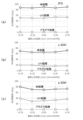
- FIG 4 shows the water contact angle of the IOH film and ITO film whose surfaces were made hydrophilic by plasma irradiation (plasma treatment) or ultraviolet light irradiation (UV treatment), together with the measured value before treatment in an untreated state.
- plasma treatment plasma irradiation
- UV treatment ultraviolet light irradiation
- the EC layer is formed on the transparent electrode layer using a wet process, so the wettability of the surface is one of the very important parameters in the manufacturing process.
- Plasma treatment was performed for 3 minutes using a plasma cleaner from Harrick Plasma.
- UV treatment was performed for 1 minute using a UV-LED light source with a wavelength of 365 nm.
- the arithmetic mean height (Sa) and maximum height (Sz) were calculated using a laser displacement meter using white light interferometry.
- c-IOH had the smallest contact angle, especially in the case of surface modification by UV treatment (ultraviolet light irradiation). Note that in the case of surface modification by plasma treatment, the water contact angle was 0° because it exceeded the measurement limit of the dynamic contact angle using a contact angle meter.
- a thin film made of tungsten oxide was formed as a first EC layer on the coated glass substrate (corresponding to the first transparent base material and the first transparent electrode layer) provided with an IOH film (multilayer film A).
- the tungsten oxide nanoparticle dispersion was measured out with a micropipette, dropped onto a 30 ⁇ 30 mm IOH-coated glass substrate placed on a spin coater, and rotated at 200 rpm for 600 seconds, then at 1600 rpm for 10 seconds to form a thin film.
- the resulting film thickness was about 600 nm (multilayer film A).
- the tungsten oxide thin film will be referred to as the WO3 thin film.
- the method of producing a tungsten oxide thin film using a tungsten oxide nanoparticle dispersion liquid as described above is superior, but there are no limitations as long as an oxidation-reduction reaction suitable for ECD can occur, and a sol-gel method using tungsten chloride, metallic tungsten, etc., or a vacuum process such as a vapor deposition method or sputtering method, which are simple physical processes, can be used.
- EC layer On the coated glass substrate (corresponding to the second transparent substrate and the second transparent electrode layer) provided with the IOH film, a thin film of a metal cyano complex was formed as an EC layer (multilayer film B).
- sample AFe1 was an aggregate of nanoparticles with a diameter of 5 to 20 nm.
- the obtained film thickness was about 1000 nm (multilayer film B).
- the iron-iron cyano complex thin film is called a PB thin film.
- multilayer film A and multilayer film B were obtained for the ITO film by the same method as for the IOH film.
- ⁇ Characteristics of the first EC layer and the second EC layer> 5 shows the spectrum of the multilayer films A and B described above for the ITO film, c-IOH film, and a-IOH film, and the spectrum of a coated glass substrate coated with only a transparent electrode layer for comparison.
- Both the multilayer film A (including a WO 3 thin film) and the multilayer film B (including a PB thin film) were affected by the transmittance of the coated glass substrate coated with the transparent electrode layer in the near infrared band.
- the multilayer film A (including a WO 3 thin film) using the c-IOH coated glass substrate, which has excellent transmittance in the near infrared band, showed a high transmittance of 70% or more at wavelengths of 1300 to 2500 nm, and the multilayer film B (including a PB thin film) showed a high transmittance of about 80% or more in the same wavelength range.
- Figure 6 shows the results of measurements of the transmission spectrum for an ECD that combines the first EC layer and second EC layer described above.
- the ECD was fabricated by sandwiching an electrolyte layer between a transparent electrode layer-coated glass substrate on which a WO3 thin film was formed and a transparent electrode layer-coated glass substrate on which a PB thin film was formed, with each glass substrate facing outward.
- the electrolyte of the electrolyte layer was prepared by adding acrylic resin to a potassium bis(trifluoromethanesulfonyl)imide (KTFSI)-propylene carbonate solution with a concentration of 0.5 mol/L to make 0.06 ml, and solidifying the electrolyte by irradiating it with ultraviolet light to form an all-solid-state element.
- KTFSI potassium bis(trifluoromethanesulfonyl)imide
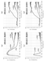
- Figure 7(a) shows the cyclic voltammograms (CV) of ECD when each transparent electrode layer was used, measured at a scan rate of 5 millivolts/second, while Figure 7(b) shows the time change in transmittance related to the color change reaction.
- the CV curve of the element using c-IOH (crystalline) almost overlaps with the curve when the existing ITO substrate was used, but in the element using a-IOH (amorphous), the timing of the applied voltage generating the peak current associated with the color change reaction was delayed. In other words, it is considered that c-IOH is more suitable as a transparent electrode layer to be used in the element.
- FIG 8(a) shows the electrochemical characteristics of the ECD measured by chronocoulometry (CC). The measurement conditions were CC1 (+1.0 V ⁇ -1.2 V x 60 seconds) and CC2 (-1.2 V ⁇ +1.0 V x 60 seconds).
- Figure 8(b) shows the results of measuring the transmittance at 60 seconds in (a). It can be seen that the charging rate is clearly slower in the element using a-IOH.
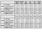
- Figure 9 shows the optical spectra of (a) the transmittance when bleached, (b) the reflectance when bleached, (c) the transmittance when colored, and (d) the reflectance when colored for the ECDs when each transparent electrode layer was used. All ECDs were bleached when a voltage of +1 V was applied, and colored when a voltage of -1.2 V was applied. Changes in optical properties. Here, measurements were taken on the day the elements were assembled, and the transmittance when bleached for the elements using c-IOH and the elements using a-IOH was about 30% in the wavelength band of about 1300 nm, which was not much higher than that of the element using an ITO film.
- Figure 10 summarizes the relevant optical properties calculated from Figure 9.
- Figure 11 shows the results of the change over time in the optical spectrum of ECDs made including each transparent electrode layer of (a) ITO, (b) c-IOH, and (c) a-IOH.
- the voltage application conditions are the same as those in Figure 9.
- the transmittance at the bleached state in the band of about 700 to 1000 nm gradually decreases with the passage of time when stored indoors. This decrease can be almost restored by performing a light aging process (irradiation with simulated sunlight or UV light for several minutes).
- the light aging process was performed by irradiating light using a xenon weather meter that emits light approximating full spectrum natural sunlight.
- the transmittance at the bleached state was initially low at about 20 to 30% in the wavelength band of 1000 nm or more, but increased to 60% or more with time.
- the transmittance at the bleached state can also be increased by performing a second light aging process. In other words, stable operation is expected by performing light aging treatment during the manufacturing process.
- Figure 12 shows the optical characteristics (transmittance when bleached) of ECD in the mid-infrared band measured using Fourier transform infrared spectroscopy.
- An element using an ITO film transmits almost no light in the mid-infrared band, but an element using an IOH film is able to maintain transmittance. In this way, by using an IOH film, it is possible to switch the optical characteristics up to the mid-infrared band and cause a color change.
- the present invention can realize an electrochromic element that can change optical properties from the near-infrared to mid-infrared band (800-4000 nm), and can perform high-contrast coloring and decoloring with a large range of change in transmittance, particularly in the near-infrared band (800-2500 nm).
- Such an element is expected to be used in light-controlling devices such as light-controlling glass, displays and display elements, and since it has improved control over long-wavelength components compared to existing technologies, it is expected to be used as a component of energy-saving light-controlling devices that optimize the inflow of infrared rays, which are the thermal components of solar energy, in window glass for automobiles and building materials.
- Electrochromic Device 10 Electrolyte layer 12a First electrochromic (EC) layer 12b Second electrochromic (EC) layer 14a First transparent electrode layer 14b Second transparent electrode layer 16a First transparent substrate 16b Second transparent substrate
Landscapes
- Physics & Mathematics (AREA)
- Nonlinear Science (AREA)
- General Physics & Mathematics (AREA)
- Optics & Photonics (AREA)
- Chemical & Material Sciences (AREA)
- Inorganic Chemistry (AREA)
- Crystallography & Structural Chemistry (AREA)
- Electrochromic Elements, Electrophoresis, Or Variable Reflection Or Absorption Elements (AREA)
Abstract
Description
前記第1透明電極層及び前記第2透明電極層は、インジウム(In)の酸化物単体、並びに、Ce、W、Ti、Zr、及びMoからなる群から選択される1種又は複数種を含むインジウム(In)の酸化物の少なくとも一方を含み、70cm2/V・s以上のキャリア移動度であり、且つ、近赤外帯域(800~2500nm)における透過率が75%以上であることを特徴とする。
ここでは高周波マグネトロンスパッタ法において、酸化インジウム(酸化インジウム単体)の焼結体をターゲットとして、水蒸気、酸素、アルゴンを含む雰囲気中で30×30mmのガラス基板上にアモルファス相を有する酸化インジウムの透明電極膜を形成させた。なお、基板の加熱は行っておらず室温で成膜し、水蒸気の導入量を1×10⁻⁴Paとした。得られた膜厚は約120nmであった。
第1透明電極層の上に第1EC層を、第2透明電極層の上に第2EC層を与えた状態での諸特性について説明する。
IOH膜を与えた被膜ガラス基板(第1透明基材及び第1透明電極層に対応)上に、第1EC層として酸化タングステンからなる薄膜を形成させた(多層膜A)。
IOH膜を与えた被膜ガラス基板(第2透明基材及び第2透明電極層に対応)上に、EC層として金属シアノ錯体の薄膜を形成させた(多層膜B)。
図5には、ITO膜とc-IOH膜とa-IOH膜とについて上記した多層膜A及びB、そして比較のための透明電極層のみを被膜した被膜ガラス基板の分光スペクトルを示す。多層膜A(WO3薄膜を含む)及び多層膜B(PB薄膜を含む)ともに、近赤外帯域の透過率では、透明電極層を被膜した被膜ガラス基板の透過率に影響を受けていた。そのため、近赤外帯域の透過率に優れるc-IOH被覆ガラス基板を用いた多層膜A(WO3薄膜を含む)では、波長1300~2500nmにおいて70%以上の高透過率、多層膜B(PB薄膜を含む)では、同波長範囲で約80%以上の高透過率を示した。
10 電解質層
12a 第1エレクトロクロミック(EC)層
12b 第2エレクトロクロミック(EC)層
14a 第1透明電極層
14b 第2透明電極層
16a 第1透明基材
16b 第2透明基材
Claims (14)
- 第1透明基材上の第1透明電極層及び第2透明基材上の第2透明電極層の間に、第1エレクトロクロミック層、電解質層、第2エレクトロクロミック層をこの順に含む、多層構造体を有する調光デバイス用エレクトロクロミック素子であって、
前記第1透明電極層及び前記第2透明電極層は、インジウム(In)の酸化物単体、並びに、Ce、W、Ti、Zr、及びMoからなる群から選択される1種又は複数種を含むインジウム(In)の酸化物の少なくとも一方を含み、70cm2/V・s以上のキャリア移動度であり、且つ、近赤外帯域(800~2500nm)における透過率が75%以上であることを特徴とする調光デバイス用エレクトロクロミック素子。 - 前記第1透明電極層及び前記第2透明電極層はアモルファス相を結晶化させた結晶相からなることを特徴とする請求項1に記載の調光デバイス用エレクトロクロミック素子。
- 前記第1透明基材及び前記第2透明基材は樹脂シートであることを特徴とする請求項2に記載の調光デバイス用エレクトロクロミック素子。
- 前記電解質層は、ビス(トリフルオロメタンスルホニル)イミド、リチウム ビス(トリフルオロメタンスルホニル)イミド、カリウム ビス(トリフルオロメタンスルホニル)イミド、ナトリウム ビス(トリフルオロメタンスルホニル)イミドのいずれか1種類以上とともに、炭酸プロピレン、炭酸エチレン、炭酸ジエチルのいずれか1種類以上の有機溶媒を含み、アクリル樹脂、エポキシ樹脂のいずれか1種類以上で固体化されており、
前記第1エレクトロクロミック層は遷移金属酸化物を含み、前記第2エレクトロクロミック層は金属シアノ錯体を含み、
前記第1透明電極層及び前記第2透明電極層への電圧の印加によって色変化を可能とすることを特徴とする請求項1乃至3のうちの1つに記載の調光デバイス用エレクトロクロミック素子。 - 前記遷移金属酸化物は、酸化タングステン、酸化モリブデン、酸化ニオブ、酸化バナジウム、酸化チタンのうちの少なくとも1種以上を含むことを特徴する請求項4に記載の調光デバイス用エレクトロクロミック素子。
- 前記金属シアノ錯体は、
Aを水素、リチウム、ナトリウム、カリウム、ルビジウム、セシウム、アンモニウムからなる群より選ばれる原子からなる陽イオン、
Mをバナジウム、クロム、マンガン、鉄、ルテニウム、コバルト、ロジウム、ニッケル、パラジウム、白金、銅、銀、亜鉛、ランタン、ユーロピウム、ガドリニウム、ルテチウム、バリウム、ストロンチウム、及びカルシウムからなる群より選ばれる金属原子、
M’を、バナジウム、クロム、モリブデン、タングステン、マンガン、鉄、ルテニウム、コバルト、ニッケル、白金、及び銅からなる群より選ばれる金属原子、
xを0~3の有理数、yを0.3~1.5の有理数、zを0~30の有理数として、
AxM[M’(CN)6]y・zH2O
の一般式で表される群より選ばれる1種又は2種以上からなるプルシアンブルー型金属錯体であることを特徴とする請求項4に記載の調光デバイス用エレクトロクロミック素子。 - 調光デバイス用エレクトロクロミック素子に用いられる透明電極層であって、
透明基材上に形成され、
インジウム(In)の酸化物単体、並びに、Ce、W、Ti、Zr、及びMoからなる群から選択される1種又は複数種を含むインジウム(In)の酸化物の少なくとも一方を含み、70cm2/V・s以上のキャリア移動度であり、且つ、近赤外帯域(800~2500nm)における透過率が75%以上であることを特徴とする透明電極層。 - 第1透明基材上の第1透明電極層及び第2透明基材上の第2透明電極層の間に、第1エレクトロクロミック層、電解質層、第2エレクトロクロミック層をこの順に含む、多層構造体を有する調光デバイス用エレクトロクロミック素子の製造方法であって、
前記第1透明基材上に前記第1透明電極層を形成する工程及び/又は前記第2透明基材上に前記第2透明電極層を形成する電極形成工程を含み、
前記電極形成工程は、
インジウム(In)の酸化物単体、並びに、Ce、W、Ti、Zr、及びMoからなる群から選択される1種又は複数種を含むインジウム(In)の酸化物の少なくとも一方を含むアモルファス相を含む前駆体膜を前記第1透明基材上及び/又は前記第2透明基材上に形成する第1工程と、
前記前駆体膜を結晶化させ、70cm2/V・s以上のキャリア移動度であり、且つ、近赤外帯域(800~2500nm)における透過率が75%以上である前記第1透明電極層及び/又は前記第2透明電極層を形成する第2工程と、を含むことを特徴とする調光デバイス用エレクトロクロミック素子の製造方法。 - 前記第2工程は、光を照射する工程を含むことを特徴とする請求項8に記載の調光デバイス用エレクトロクロミック素子の製造方法。
- 前記第2工程は、100℃以下の温度で処理する工程であることを特徴とする請求項9に記載の調光デバイス用エレクトロクロミック素子の製造方法。
- 前記第1透明基材及び前記第2透明基材は樹脂シートであることを特徴とする請求項9又は10に記載の調光デバイス用エレクトロクロミック素子の製造方法。
- 前記電解質層は、ビス(トリフルオロメタンスルホニル)イミド、リチウム ビス(トリフルオロメタンスルホニル)イミド、カリウム ビス(トリフルオロメタンスルホニル)イミド、ナトリウム ビス(トリフルオロメタンスルホニル)イミドのいずれか1種類以上とともに、炭酸プロピレン、炭酸エチレン、炭酸ジエチルのいずれか1種類以上の有機溶媒を含み、アクリル樹脂、エポキシ樹脂のいずれか1種類以上で固体化されており、
前記第1エレクトロクロミック層は遷移金属酸化物を含み、前記第2エレクトロクロミック層は金属シアノ錯体を含み、
前記調光デバイス用エレクトロクロミック素子は前記第1透明電極層及び前記第2透明電極層への電圧の印加によって色変化を可能とすることを特徴とする請求項8に記載の調光デバイス用エレクトロクロミック素子の製造方法。 - 前記多層構造体を形成後、光照射する光エージング処理工程を含むことを特徴とする請求項8に記載の調光デバイス用エレクトロクロミック素子の製造方法。
- 調光デバイス用エレクトロクロミック素子に用いられる透明電極層の製造方法であって、
透明基材上に透明電極層を形成する電極形成工程を含み、
前記電極形成工程は、
インジウム(In)の酸化物単体、並びに、Ce、W、Ti、Zr、及びMoからなる群から選択される1種又は複数種を含むインジウム(In)の酸化物の少なくとも一方を含むアモルファス相を有する前駆体膜を前記透明基材上に形成する第1工程と、
前記前駆体膜を結晶化させ、70cm2/V・s以上のキャリア移動度であり、且つ、近赤外帯域(800~2500nm)における透過率が75%以上である前記透明電極層を形成する第2工程と、を含むことを特徴とする透明電極層の製造方法。
Priority Applications (2)
| Application Number | Priority Date | Filing Date | Title |
|---|---|---|---|
| EP24843024.1A EP4745658A1 (en) | 2023-07-14 | 2024-07-09 | Electrochromic element for a light control device, method for manufacturing an electrochromic element for a light control device, transparent electrode layer, and method for manufacturing a transparent electrode layer |
| JP2025534002A JPWO2025018232A1 (ja) | 2023-07-14 | 2024-07-09 |
Applications Claiming Priority (2)
| Application Number | Priority Date | Filing Date | Title |
|---|---|---|---|
| JP2023115853 | 2023-07-14 | ||
| JP2023-115853 | 2023-07-14 |
Publications (1)
| Publication Number | Publication Date |
|---|---|
| WO2025018232A1 true WO2025018232A1 (ja) | 2025-01-23 |
Family
ID=94282156
Family Applications (1)
| Application Number | Title | Priority Date | Filing Date |
|---|---|---|---|
| PCT/JP2024/024824 Ceased WO2025018232A1 (ja) | 2023-07-14 | 2024-07-09 | 調光デバイス用エレクトロクロミック素子、調光デバイス用エレクトロクロミック素子の製造方法、透明電極層、及び、透明電極層の製造方法 |
Country Status (3)
| Country | Link |
|---|---|
| EP (1) | EP4745658A1 (ja) |
| JP (1) | JPWO2025018232A1 (ja) |
| WO (1) | WO2025018232A1 (ja) |
Citations (7)
| Publication number | Priority date | Publication date | Assignee | Title |
|---|---|---|---|---|
| JPS62126506A (ja) * | 1985-11-27 | 1987-06-08 | 株式会社日立製作所 | 透明導電膜改質方法 |
| JP2006286308A (ja) * | 2005-03-31 | 2006-10-19 | Toppan Printing Co Ltd | 透明導電膜積層体およびその製造方法 |
| JP2008107587A (ja) | 2006-10-26 | 2008-05-08 | Sumitomo Metal Mining Co Ltd | エレクトロクロミック素子及びその製造方法 |
| WO2018025939A1 (ja) * | 2016-08-02 | 2018-02-08 | 国立研究開発法人産業技術総合研究所 | エレクトロクロミック素子及びエレクトロクロミック材料 |
| KR20180045155A (ko) * | 2016-10-25 | 2018-05-04 | 한밭대학교 산학협력단 | 스퍼터링 타겟 및 투명 도전막의 제조방법 |
| JP2018120199A (ja) * | 2016-05-13 | 2018-08-02 | 株式会社リコー | エレクトロクロミック装置 |
| JP2018185424A (ja) | 2017-04-26 | 2018-11-22 | 国立研究開発法人産業技術総合研究所 | エレクトロクロミック素子及びそれを用いた調光部材 |
-
2024
- 2024-07-09 JP JP2025534002A patent/JPWO2025018232A1/ja active Pending
- 2024-07-09 EP EP24843024.1A patent/EP4745658A1/en active Pending
- 2024-07-09 WO PCT/JP2024/024824 patent/WO2025018232A1/ja not_active Ceased
Patent Citations (7)
| Publication number | Priority date | Publication date | Assignee | Title |
|---|---|---|---|---|
| JPS62126506A (ja) * | 1985-11-27 | 1987-06-08 | 株式会社日立製作所 | 透明導電膜改質方法 |
| JP2006286308A (ja) * | 2005-03-31 | 2006-10-19 | Toppan Printing Co Ltd | 透明導電膜積層体およびその製造方法 |
| JP2008107587A (ja) | 2006-10-26 | 2008-05-08 | Sumitomo Metal Mining Co Ltd | エレクトロクロミック素子及びその製造方法 |
| JP2018120199A (ja) * | 2016-05-13 | 2018-08-02 | 株式会社リコー | エレクトロクロミック装置 |
| WO2018025939A1 (ja) * | 2016-08-02 | 2018-02-08 | 国立研究開発法人産業技術総合研究所 | エレクトロクロミック素子及びエレクトロクロミック材料 |
| KR20180045155A (ko) * | 2016-10-25 | 2018-05-04 | 한밭대학교 산학협력단 | 스퍼터링 타겟 및 투명 도전막의 제조방법 |
| JP2018185424A (ja) | 2017-04-26 | 2018-11-22 | 国立研究開発法人産業技術総合研究所 | エレクトロクロミック素子及びそれを用いた調光部材 |
Also Published As
| Publication number | Publication date |
|---|---|
| JPWO2025018232A1 (ja) | 2025-01-23 |
| EP4745658A1 (en) | 2026-05-20 |
Similar Documents
| Publication | Publication Date | Title |
|---|---|---|
| Jia et al. | Electrochromic windows with fast response and wide dynamic range for visible-light modulation without traditional electrodes | |
| Dokouzis et al. | Photoelectrochromic devices with cobalt redox electrolytes | |
| Bonhôte et al. | Novel electrochromic devices based on complementary nanocrystalline TiO2 and WO3 thin films | |
| Gillaspie et al. | Metal-oxide films for electrochromic applications: present technology and future directions | |
| Granqvist et al. | Recent advances in electrochromics for smart windows applications | |
| JP2014524055A (ja) | エレクトロクロミックナノコンポジット薄膜 | |
| EP1247137A1 (en) | Self bleaching photoelectrochemical-electrochromic device | |
| US7333258B2 (en) | Electrochromic material | |
| Kumar et al. | Effect of annealing and oxygen partial pressure on the RF sputtered WO3 thin films for electrochromic applications | |
| CN114647122B (zh) | 一种高性能可见红外独立调控电致变色器件及其制备方法和应用 | |
| Ali et al. | Electrochromic displays via the room-temperature electrochemical oxidation of nickel | |
| JP7352987B2 (ja) | エレクトロクロミック素子 | |
| US20190146294A1 (en) | Electrochromic electrodes and methods of making and use thereof | |
| JP2003270671A (ja) | エレクトロクロミック装置 | |
| US8609981B2 (en) | P-type transparent conductive oxide for solar cell comprising molybdenum trioxide doped with indium | |
| Patel et al. | Highly Transparent Spectral Tunable Electrochromic Window Based on Solid‐State WO3 Thin Films | |
| US9904137B1 (en) | Electrochromic materials and fabrication methods | |
| JP2003270670A (ja) | エレクトロクロミック装置 | |
| Kang et al. | Dual-functional electrochromic-energy storage devices with superior long-term stability via slot-die coated niobium tungsten oxide films | |
| Zhao et al. | Synergistic enhancement of WO3 electrochromic properties by carbon-doped induced oxygen vacancies and localized surface plasmon resonance of metallic copper | |
| Tan et al. | Electrochromic Smart Windows: An Energy-Efficient Technology | |
| Lou et al. | Toward durably flexible nickel oxide electrochromic film by covering an 18 nm zinc tin oxide buffer layer | |
| JP2003255400A (ja) | エレクトロクロミック装置 | |
| JP4846296B2 (ja) | エレクトロクロミック表示素子 | |
| JP2003315840A (ja) | エレクトロクロミックディスプレイ |
Legal Events
| Date | Code | Title | Description |
|---|---|---|---|
| 121 | Ep: the epo has been informed by wipo that ep was designated in this application |
Ref document number: 24843024 Country of ref document: EP Kind code of ref document: A1 |
|
| ENP | Entry into the national phase |
Ref document number: 2025534002 Country of ref document: JP Kind code of ref document: A |
|
| WWE | Wipo information: entry into national phase |
Ref document number: 2025534002 Country of ref document: JP |
|
| WWE | Wipo information: entry into national phase |
Ref document number: 2024843024 Country of ref document: EP |
|
| NENP | Non-entry into the national phase |
Ref country code: DE |