WO2025013622A1 - 表示装置及び表示装置の製造方法 - Google Patents
表示装置及び表示装置の製造方法 Download PDFInfo
- Publication number
- WO2025013622A1 WO2025013622A1 PCT/JP2024/023090 JP2024023090W WO2025013622A1 WO 2025013622 A1 WO2025013622 A1 WO 2025013622A1 JP 2024023090 W JP2024023090 W JP 2024023090W WO 2025013622 A1 WO2025013622 A1 WO 2025013622A1
- Authority
- WO
- WIPO (PCT)
- Prior art keywords
- light
- emitting element
- layer
- emitting
- electrode
- Prior art date
- Legal status (The legal status is an assumption and is not a legal conclusion. Google has not performed a legal analysis and makes no representation as to the accuracy of the status listed.)
- Pending
Links
Images




























Classifications
-
- H—ELECTRICITY
- H10—SEMICONDUCTOR DEVICES; ELECTRIC SOLID-STATE DEVICES NOT OTHERWISE PROVIDED FOR
- H10K—ORGANIC ELECTRIC SOLID-STATE DEVICES
- H10K50/00—Organic light-emitting devices
- H10K50/10—OLEDs or polymer light-emitting diodes [PLED]
-
- H—ELECTRICITY
- H10—SEMICONDUCTOR DEVICES; ELECTRIC SOLID-STATE DEVICES NOT OTHERWISE PROVIDED FOR
- H10K—ORGANIC ELECTRIC SOLID-STATE DEVICES
- H10K50/00—Organic light-emitting devices
- H10K50/80—Constructional details
- H10K50/805—Electrodes
- H10K50/81—Anodes
- H10K50/818—Reflective anodes, e.g. ITO combined with thick metallic layers
-
- H—ELECTRICITY
- H10—SEMICONDUCTOR DEVICES; ELECTRIC SOLID-STATE DEVICES NOT OTHERWISE PROVIDED FOR
- H10K—ORGANIC ELECTRIC SOLID-STATE DEVICES
- H10K50/00—Organic light-emitting devices
- H10K50/80—Constructional details
- H10K50/805—Electrodes
- H10K50/82—Cathodes
- H10K50/828—Transparent cathodes, e.g. comprising thin metal layers
-
- H—ELECTRICITY
- H10—SEMICONDUCTOR DEVICES; ELECTRIC SOLID-STATE DEVICES NOT OTHERWISE PROVIDED FOR
- H10K—ORGANIC ELECTRIC SOLID-STATE DEVICES
- H10K50/00—Organic light-emitting devices
- H10K50/80—Constructional details
- H10K50/85—Arrangements for extracting light from the devices
- H10K50/852—Arrangements for extracting light from the devices comprising a resonant cavity structure, e.g. Bragg reflector pair
-
- H—ELECTRICITY
- H10—SEMICONDUCTOR DEVICES; ELECTRIC SOLID-STATE DEVICES NOT OTHERWISE PROVIDED FOR
- H10K—ORGANIC ELECTRIC SOLID-STATE DEVICES
- H10K50/00—Organic light-emitting devices
- H10K50/80—Constructional details
- H10K50/85—Arrangements for extracting light from the devices
- H10K50/856—Arrangements for extracting light from the devices comprising reflective means
-
- H—ELECTRICITY
- H10—SEMICONDUCTOR DEVICES; ELECTRIC SOLID-STATE DEVICES NOT OTHERWISE PROVIDED FOR
- H10K—ORGANIC ELECTRIC SOLID-STATE DEVICES
- H10K59/00—Integrated devices, or assemblies of multiple devices, comprising at least one organic light-emitting element covered by group H10K50/00
- H10K59/10—OLED displays
- H10K59/12—Active-matrix OLED [AMOLED] displays
- H10K59/121—Active-matrix OLED [AMOLED] displays characterised by the geometry or disposition of pixel elements
-
- H—ELECTRICITY
- H10—SEMICONDUCTOR DEVICES; ELECTRIC SOLID-STATE DEVICES NOT OTHERWISE PROVIDED FOR
- H10K—ORGANIC ELECTRIC SOLID-STATE DEVICES
- H10K59/00—Integrated devices, or assemblies of multiple devices, comprising at least one organic light-emitting element covered by group H10K50/00
- H10K59/10—OLED displays
- H10K59/12—Active-matrix OLED [AMOLED] displays
- H10K59/122—Pixel-defining structures or layers, e.g. banks
-
- H—ELECTRICITY
- H10—SEMICONDUCTOR DEVICES; ELECTRIC SOLID-STATE DEVICES NOT OTHERWISE PROVIDED FOR
- H10K—ORGANIC ELECTRIC SOLID-STATE DEVICES
- H10K59/00—Integrated devices, or assemblies of multiple devices, comprising at least one organic light-emitting element covered by group H10K50/00
- H10K59/30—Devices specially adapted for multicolour light emission
- H10K59/35—Devices specially adapted for multicolour light emission comprising red-green-blue [RGB] subpixels
-
- H—ELECTRICITY
- H10—SEMICONDUCTOR DEVICES; ELECTRIC SOLID-STATE DEVICES NOT OTHERWISE PROVIDED FOR
- H10K—ORGANIC ELECTRIC SOLID-STATE DEVICES
- H10K2102/00—Constructional details relating to the organic devices covered by this subclass
- H10K2102/10—Transparent electrodes, e.g. using graphene
Definitions
- This disclosure relates to a display device and a method for manufacturing a display device.
- Such display devices have multiple light-emitting elements, each composed of, for example, a lower electrode, a light-emitting layer stacked on the lower electrode, and an upper electrode stacked on the light-emitting layer.
- EL electroluminescence
- Such display devices have multiple light-emitting elements, each composed of, for example, a lower electrode, a light-emitting layer stacked on the lower electrode, and an upper electrode stacked on the light-emitting layer.
- the display device described in the following patent document can be cited as an example of such a display device.
- This disclosure therefore proposes a display device and a method for manufacturing the display device that can improve light extraction efficiency while minimizing an increase in the number of steps.
- a display device comprising a plurality of light-emitting elements including a first light-emitting element and a second light-emitting element that emit light of different colors, and a plurality of element isolation layers arranged to surround an element region in which each of the plurality of light-emitting elements is located, each of the light-emitting elements having a first reflecting surface, a light-emitting portion stacked above the first reflecting surface, an optical adjustment layer stacked above the light-emitting portion so as to be embedded in the element region surrounded by the element isolation layer, and a second reflecting surface stacked above the optical adjustment layer and made of a semi-transparent reflective material, wherein the area of the element region of the first light-emitting element surrounded by the element isolation layer is different from the area of the element region of the second light-emitting element surrounded by the element isolation layer, and the film thickness of the optical adjustment layer of the first light-emitting element is different from the film thickness of the optical adjustment layer of the
- a method for manufacturing a display device including a plurality of light-emitting elements including a first light-emitting element and a second light-emitting element that emit light of different colors, and a plurality of element isolation layers provided to surround an element region in which each of the plurality of light-emitting elements is located, the method including stacking a light-emitting section above a first reflecting surface on a substrate, stacking an element isolation layer to surround an element region on the light-emitting section in which each of the light-emitting elements is formed, stacking an optical adjustment layer to be embedded in the element region surrounded by the element isolation layer, and stacking a second reflecting surface made of a semi-transparent reflective material above the optical adjustment layer, and stacking the element isolation layer such that the area of the element region of the first light-emitting element surrounded by the element isolation layer is different from the area of the element region of the second light-emitting element surrounded by the element isolation layer, thereby making the film
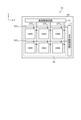
- FIG. 1 is a schematic diagram illustrating an example of an overall configuration of a display device according to an embodiment of the present disclosure.
- FIG. 11 is a schematic circuit diagram for explaining a wiring relationship in a sub-pixel in the mth row and the nth column.
- FIG. 1 is an explanatory diagram (part 1) for explaining the background that led to the creation of an embodiment of the present disclosure.
- FIG. 2 is an explanatory diagram (part 2) for explaining the background that led to the creation of the embodiment of the present disclosure.
- 1 is a cross-sectional view for explaining an example of a configuration of a light-emitting element according to a first embodiment of the present disclosure.
- FIG. 2 is a plan view for explaining an example of a configuration of a light-emitting element according to the first embodiment of the present disclosure.
- FIG. 2 is an explanatory diagram (part 1) for explaining a manufacturing method of the light-emitting element according to the first embodiment of the present disclosure.
- FIG. 4 is an explanatory diagram (part 2) for explaining the manufacturing method of the light-emitting element according to the first embodiment of the present disclosure.
- FIG. 4 is an explanatory diagram (part 3) for explaining the manufacturing method of the light-emitting element according to the first embodiment of the present disclosure.
- FIG. 4 is an explanatory diagram (part 4) for explaining the manufacturing method of the light-emitting element according to the first embodiment of the present disclosure.
- 1 is a cross-sectional view for explaining an example of a configuration of a main part of a light-emitting element according to Modification 1 of the first embodiment of the present disclosure.
- FIG. 11 is a cross-sectional view (part 1) for explaining an example of a configuration of a light-emitting element according to Modification 2 of the first embodiment of the present disclosure.
- FIG. 11 is a cross-sectional view (part 2) for explaining an example of a configuration of a light-emitting element according to Modification 2 of the first embodiment of the present disclosure.
- FIG. 11 is a cross-sectional view (part 3) for explaining an example of a configuration of a light-emitting element according to Modification 2 of the first embodiment of the present disclosure.
- FIG. 11 is a cross-sectional view (part 4) for explaining an example of the configuration of a light-emitting element according to Modification 2 of the first embodiment of the present disclosure.
- FIG. 11 is a cross-sectional view (part 1) for explaining an example of a configuration of a light-emitting element according to Modification 2 of the first embodiment of the present disclosure.
- FIG. 11 is a cross-sectional view (part 2) for explaining an example
- FIG. 5 is a cross-sectional view (part 5) for explaining an example of a configuration of a light-emitting element according to Modification 2 of the first embodiment of the present disclosure.
- FIG. 6 is a cross-sectional view (part 6) for explaining an example of the configuration of a light-emitting element according to Modification 2 of the first embodiment of the present disclosure.
- FIG. 7 is a cross-sectional view (part 7) for explaining an example of the configuration of a light-emitting element according to Modification 2 of the first embodiment of the present disclosure.
- FIG. 8 is a cross-sectional view (part 8) for explaining an example of a configuration of a light-emitting element according to Modification 2 of the first embodiment of the present disclosure.
- FIG. 8 is a cross-sectional view (part 8) for explaining an example of a configuration of a light-emitting element according to Modification 2 of the first embodiment of the present disclosure.
- FIG. 9 is a cross-sectional view for explaining an example of a configuration of a light-emitting element according to Modification 2 of the first embodiment of the present disclosure.
- FIG. 11 is a cross-sectional view (part 1) for explaining an example of a configuration of a main part of a light-emitting element according to Modification 3 of the first embodiment of the present disclosure.
- FIG. 11 is a cross-sectional view (part 2) for explaining an example of a configuration of a main part of a light-emitting element according to Modification 3 of the first embodiment of the present disclosure.
- FIG. 11 is a cross-sectional view for explaining an example of a configuration of a light-emitting element according to Modification 4 of the first embodiment of the present disclosure.
- FIG. 11 is a cross-sectional view for explaining an example of a configuration of a light-emitting element according to Modification 4 of the first embodiment of the present disclosure.
- FIG. 13 is a plan view for explaining an example of a configuration of a light-emitting element according to Modification 4 of the first embodiment of the present disclosure.
- FIG. 11 is a cross-sectional view (part 1) for explaining an example of a configuration of a light-emitting element according to Modification 5 of the first embodiment of the present disclosure.
- FIG. 13 is a cross-sectional view (part 2) for explaining an example of the configuration of a light-emitting element according to Modification 5 of the first embodiment of the present disclosure.
- FIG. 13 is a cross-sectional view (part 1) for explaining an example of a configuration of a light-emitting element according to Modification 6 of the first embodiment of the present disclosure.
- FIG. 11 is a cross-sectional view (part 1) for explaining an example of a configuration of a light-emitting element according to Modification 5 of the first embodiment of the present disclosure.
- FIG. 13 is a cross-sectional view (part 1) for explaining an example of a configuration of a light
- FIG. 23 is a cross-sectional view (part 2) for explaining an example of the configuration of a light-emitting element according to Modification 6 of the first embodiment of the present disclosure.
- FIG. 13 is a cross-sectional view for explaining an example of the configuration of a light-emitting element according to Modification 7 of the first embodiment of the present disclosure. 13 is a cross-sectional view for explaining an example of a configuration of a main part of a light-emitting element according to Modification 7 of the first embodiment of the present disclosure.
- FIG. FIG. 13 is a cross-sectional view (part 1) for explaining an example of a configuration of a light-emitting element according to Modification 8 of the first embodiment of the present disclosure.
- FIG. 23 is a cross-sectional view (part 2) for explaining an example of the configuration of a light-emitting element according to Modification 8 of the first embodiment of the present disclosure.
- FIG. 13 is a cross-sectional view (part 3) for explaining an example of the configuration of a light-emitting element according to Modification 8 of the first embodiment of the present disclosure.
- FIG. 13 is a plan view for explaining an example of a configuration of a light-emitting element according to Modification 9 of the first embodiment of the present disclosure.
- FIG. 23 is a cross-sectional view (part 1) for explaining an example of the configuration of a light-emitting element according to a tenth modification of the first embodiment of the present disclosure.
- FIG. 13 is a plan view for explaining an example of a configuration of a light-emitting element according to Modification 10 of the first embodiment of the present disclosure.
- FIG. FIG. 23 is a cross-sectional view (part 2) for explaining an example of the configuration of a light-emitting element according to Modification 10 of the first embodiment of the present disclosure.
- FIG. 11 is a cross-sectional view for explaining an example of the configuration of a light-emitting element according to a second embodiment of the present disclosure.
- 11A to 11C are explanatory views (part 1) for explaining a manufacturing method of a light-emitting element according to a second embodiment of the present disclosure.
- FIG. 13 is an explanatory diagram (part 2) for explaining the manufacturing method of the light-emitting element according to the second embodiment of the present disclosure.
- FIG. 11 is an explanatory diagram (part 3) for explaining the manufacturing method of the light-emitting element according to the second embodiment of the present disclosure.
- FIG. 11 is an explanatory diagram (part 4) for explaining the manufacturing method of the light-emitting element according to the second embodiment of the present disclosure.
- FIG. 5 is an explanatory diagram (part 5) for explaining the manufacturing method of the light-emitting element according to the second embodiment of the present disclosure.
- FIG. 6 is an explanatory diagram (part 6) for explaining the manufacturing method of the light-emitting element according to the second embodiment of the present disclosure.
- FIG. 13 is a plan view for explaining an example of a configuration of a main part of a light-emitting element according to Modification 1 of the second embodiment of the present disclosure.
- FIG. 11 is a cross-sectional view (part 1) for explaining an example of a configuration of a light-emitting element according to Modification 2 of the second embodiment of the present disclosure.
- FIG. 13 is a cross-sectional view (part 2) for explaining an example of a configuration of a light-emitting element according to Modification 2 of the second embodiment of the present disclosure.
- FIG. 13 is a cross-sectional view (part 3) for explaining an example of a configuration of a light-emitting element according to Modification 2 of the second embodiment of the present disclosure.
- FIG. 11 is a cross-sectional view (part 1) for explaining an example of a configuration of a light-emitting element according to Modification 2 of the second embodiment of the present disclosure.
- FIG. 13 is a cross-sectional view (part 2) for explaining an example of
- FIG. 13 is a cross-sectional view (part 4) for explaining an example of the configuration of a light-emitting element according to Modification 2 of the second embodiment of the present disclosure.
- FIG. 5 is a cross-sectional view (part 5) for explaining an example of the configuration of a light-emitting element according to Modification 2 of the second embodiment of the present disclosure.
- FIG. 13 is a cross-sectional view (part 6) for explaining an example of the configuration of a light-emitting element according to Modification 2 of the second embodiment of the present disclosure.
- FIG. 13 is a cross-sectional view (part 7) for explaining an example of the configuration of a light-emitting element according to Modification 2 of the second embodiment of the present disclosure.
- FIG. 8 is a cross-sectional view (part 8) for explaining an example of the configuration of a light-emitting element according to Modification 2 of the second embodiment of the present disclosure.
- FIG. 11 is a cross-sectional view for explaining an example of a configuration of a light-emitting element according to Modification 3 of the second embodiment of the present disclosure.
- FIG. 13 is a plan view for explaining an example of a configuration of a light-emitting element according to Modification 3 of the second embodiment of the present disclosure.
- FIG. 13 is a plan view for explaining an example of a configuration of a light-emitting element according to Modification 4 of the second embodiment of the present disclosure.
- FIG. 13 is a cross-sectional view for explaining an example of a configuration of a light-emitting element according to Modification 5 of the second embodiment of the present disclosure.
- FIG. 11 is a cross-sectional view for explaining an example of the configuration of a light-emitting element according to a third embodiment of the present disclosure.
- FIG. 13 is a cross-sectional view for explaining an example of a configuration of a light-emitting element according to a modified example of the third embodiment of the present disclosure.
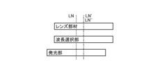
- FIG. 11 is a conceptual diagram (part 1) for explaining the relationship between a normal line LN passing through the center of a light-emitting portion, a normal line LN' passing through the center of a lens member, and a normal line LN" passing through the center of a wavelength selection portion.
- FIG. 2 is a conceptual diagram (part 2) for explaining the relationship between a normal line LN passing through the center of the light-emitting portion, a normal line LN' passing through the center of the lens member, and a normal line LN" passing through the center of the wavelength selection portion.
- FIG. 1 for explaining the relationship between a normal line LN passing through the center of a light-emitting portion, a normal line LN' passing through the center of a lens member, and a normal line LN" passing through the center of the wavelength selection portion.
- FIG. 11 is a conceptual diagram (part 3) for explaining the relationship between a normal line LN passing through the center of the light-emitting portion, a normal line LN' passing through the center of the lens member, and a normal line LN" passing through the center of the wavelength selection portion.
- FIG. 4 is a conceptual diagram (part 4) for explaining the relationship between a normal line LN passing through the center of the light-emitting portion, a normal line LN' passing through the center of the lens member, and a normal line LN" passing through the center of the wavelength selection portion.
- FIG. 4 is a conceptual diagram (part 4) for explaining the relationship between a normal line LN passing through the center of the light-emitting portion, a normal line LN' passing through the center of the lens member, and a normal line LN" passing through the center of the wavelength selection portion.
- FIG. 5 is a conceptual diagram (part 5) for explaining the relationship between a normal line LN passing through the center of the light-emitting portion, a normal line LN' passing through the center of the lens member, and a normal line LN" passing through the center of the wavelength selection portion.
- FIG. 6 is a conceptual diagram (part 6) for explaining the relationship between a normal line LN passing through the center of the light-emitting portion, a normal line LN' passing through the center of the lens member, and a normal line LN" passing through the center of the wavelength selection portion.
- FIG. 6 is a conceptual diagram (part 6) for explaining the relationship between a normal line LN passing through the center of the light-emitting portion, a normal line LN' passing through the center of the lens member, and a normal line LN" passing through the center of the wavelength selection portion.
- FIG. 7 is a conceptual diagram (part 7) for explaining the relationship between a normal line LN passing through the center of the light-emitting portion, a normal line LN' passing through the center of the lens member, and a normal line LN" passing through the center of the wavelength selection portion.
- 1 is a schematic cross-sectional view for explaining a first example of a resonator structure.
- FIG. 11 is a schematic cross-sectional view for explaining a second example of a resonator structure.
- FIG. 13 is a schematic cross-sectional view for explaining a third example of a resonator structure.
- FIG. 13 is a schematic cross-sectional view for explaining a fourth example of a resonator structure.
- FIG. 13 is a schematic cross-sectional view for explaining a fifth example of a resonator structure.
- FIG. 13 is a schematic cross-sectional view for explaining a sixth example of a resonator structure.
- FIG. 13 is a schematic cross-sectional view for explaining a seventh example of a resonator structure.
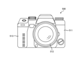
- FIG. 1 is a front view showing an example of the appearance of a digital still camera.
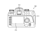
- FIG. 2 is a rear view showing an example of the appearance of a digital still camera.
- FIG. 1 is an external view of a head mounted display.
- FIG. 1 is an external view of a see-through head-mounted display.
- FIG. 1 is an external view of a television device.
- FIG. 1 is an external view of a smartphone.
- FIG. 1 is a diagram showing the internal structure of a vehicle.
- FIG. 2 is a diagram showing the internal structure of a vehicle (part 2).
- circuits electrical connections
- electrically connected means connecting multiple elements so that electricity (signals) is conducted between them.
- electrically connected includes not only cases where multiple elements are directly and electrically connected, but also cases where elements are indirectly and electrically connected via other elements.
- Fig. 1 is a schematic diagram showing an example of the overall configuration of the display device 10 according to an embodiment of the present disclosure.
- the display device 10 is a device in which light-emitting elements such as OLEDs (Organic Light Emitting Diodes) or Micro-OLEDs are formed in an array.
- a display device 10 can be used as a display device, for example, a display device for VR (Virtual Reality), MR (Mixed Reality), or AR (Augmented Reality), an electronic viewfinder (EVF), or a small projector.
- the display device 10 can also be used in various lighting devices.
- the display device 10 may be a device that uses light-emitting elements made of inorganic materials instead of light-emitting elements made of organic materials such as OLEDs.
- the display device 10 has a display area and a peripheral area provided on the periphery of the display area. As shown in FIG. 1, within the display area of the display device 10, for example, a plurality of sub-pixels 100R, 100G, and 100B are arranged in a matrix.
- the sub-pixel 100R can emit red light
- the sub-pixel 100G can emit green light
- the sub-pixel 100B can emit blue light.
- sub-pixels 100 when there is no particular need to distinguish between the sub-pixels 100R, 100G, and 100B, they will be referred to as sub-pixels 100.
- one pixel 20 is configured by combining, for example, three types of sub-pixels 100R, 100G, and 100B that emit different light.
- the number and arrangement of the three types of sub-pixels 100R, 100G, and 100B included in one pixel 20 are not particularly limited.
- one pixel 20 is not limited to being configured by multiple sub-pixels 100 that emit different light as described above, but may be configured by multiple sub-pixels 100 that emit the same color light.
- the pixel 20 means the smallest unit (pixel) controlled during the light emission control of the display device 10, and is configured by multiple sub-pixels 100 that are treated as one unit during control. That is, in this embodiment, the display device 10 has multiple pixels 20 arranged in a matrix on the substrate 40.
- a horizontal drive circuit 11 and a vertical drive circuit 12 are provided in the peripheral area of the display device 10.
- the horizontal drive circuit 11 can scan the sub-pixels 100 in row units (in FIG. 1, the direction extending along the X direction is called the row direction) when writing signals to the sub-pixels 100, and sequentially supply scanning signals to each scanning line SCLm.
- the horizontal drive circuit 11 can be configured, for example, with a shift register that sequentially shifts (transfers) a start pulse in synchronization with an input clock pulse.
- the vertical drive circuit 12 can also supply a signal voltage of a signal corresponding to luminance information supplied from a signal supply source (not shown) to the sub-pixels 100 selected in column units (in FIG. 1, the direction extending along the Y direction is called the column direction) via the signal lines DTLn.
- the configuration of the display device 10 is not limited to the configuration shown in FIG. 1.
- the configuration shown in FIG. 1 is merely an example, and the display device 10 according to the embodiment of the present disclosure can have various configurations.
- FIG. 2 is a schematic circuit diagram for explaining the wiring relationship in the sub-pixel 100 in the mth row and nth column.
- the sub-pixels 100 including the light-emitting elements ELP are arranged in a two-dimensional matrix while being connected to the scanning lines SCLm extending in the row direction (X direction in FIG. 1) and the signal lines DTLn extending in the column direction (Y direction in FIG. 1).
- the display device 10 has a power supply line PS1m that supplies a drive voltage to the sub-pixels 100, and a common power supply line PS2 that is commonly connected to all of the sub-pixels 100.
- a predetermined drive voltage Vcc or the like is supplied to the power supply line PS1m from a power supply unit (not shown), and a common voltage Vcat (e.g., ground potential) is supplied to the common power supply line PS2.
- the number of scanning lines SCL and power supply lines PS1 is M each.
- the number of signal lines DTL is N.
- the sub-pixel 100 located in the mth row and nth column may be referred to as the (n, m)th sub-pixel 100.
- the display device 10 is scanned sequentially row by row by the scanning signal from the horizontal drive circuit 11. More specifically, in the display device 10, M sub-pixels 100 arranged in the mth row are driven simultaneously. In other words, the timing of emission/non-emission of M sub-pixels 100 arranged along the row direction is controlled for each row to which they belong. For example, if the display frame rate of the display device 10 is FR (times/second), the scanning period per row (so-called horizontal scanning period) when the display device 10 is scanned sequentially row by row is less than (1/FR) x (1/P) seconds.
- the subpixel 100 is composed of a light-emitting element ELP and a drive circuit that drives it.
- the light-emitting element ELP is an organic electroluminescence light-emitting element or an inorganic electroluminescence light-emitting element.
- the drive circuit is composed of a write transistor TRW, a drive transistor TRD, and a capacitance section C1. When a current flows through the light-emitting element ELP via the drive transistor TRD, the light-emitting element ELP can emit light.
- Each transistor is composed of, for example, a p-channel type field effect transistor.
- one source/drain region of the drive transistor TRD is electrically connected to one end of the capacitance unit C1 and the power supply line PS1m, and the other source/drain region is electrically connected to one end (specifically, the anode electrode) of the light-emitting element ELP.
- the gate electrode of the drive transistor TRD is connected to the other source/drain region of the write transistor TRW and is also electrically connected to the other end of the capacitance unit C1.
- one of the source/drain regions of the write transistor TRw is electrically connected to the signal line DTLn, and the gate electrode of the write transistor TRw is electrically connected to the scan line SCLm.
- the other end of the light-emitting element ELP (specifically, the cathode electrode) is electrically connected to a common power supply line PS2. Furthermore, a predetermined cathode voltage Vcat is supplied to the common power supply line PS2. Note that in FIG. 2, the capacitance of the light-emitting element ELP is represented by the symbol CEL.
- the sub-pixel 100 when a voltage corresponding to the brightness of an image to be displayed is supplied to the signal line DTLn from the vertical drive circuit 12 and the writing transistor TRw is made conductive by a scanning signal from the horizontal drive circuit 11, a voltage corresponding to the brightness is written to the capacitance section C1. After the writing transistor TRw is made non-conductive, a current flows through the driving transistor TRD according to the voltage held in the capacitance section C1, causing the light-emitting element ELP to emit light.
- the configuration of the drive circuit that controls the light emission of the light-emitting element ELP is not limited to the configuration shown in FIG. 2. Therefore, the configuration shown in FIG. 2 is merely an example, and various configurations can be used in the display device 10 according to the embodiment of the present disclosure.
- light-emitting elements such as OLEDs (Organic Light-Emitting Diodes) have come to be used not only in direct-view display devices such as monitors, but also in ultra-small display devices (microdisplays) that require a pixel pitch of several microns.
- OLEDs Organic Light-Emitting Diodes
- sub-pixels 100R, 100G, and 100B are formed by painting red, green, and blue (RGB painting) using a mask deposition process.
- RGB painting red, green, and blue
- the RGB painting technique using a mask deposition process has limitations in terms of the accuracy of mask alignment, and therefore is limited in its ability to accommodate fine pixel pitches. Therefore, it has been proposed to avoid using the RGB painting technique and use a White-type structure in which light-emitting layers of three colors, red, green, and blue, are stacked across all sub-pixels 100 to extract white light.
- the White method is configured with a common layer structure that is common to all sub-pixels 100R, 100G, and 100B, making it difficult to optimize the structure for each color of emitted light, and there are limitations to improving the light extraction efficiency.
- the distance between the anode electrode (first electrode) 202 functioning as a reflective film and the semi-transmissive reflective film 210 is optimized for each of the sub-pixels 100R, 100G, and 100B, and light from the light-emitting portion 204 is resonated between the anode electrode 202 and the semi-transmissive reflective film 210.
- the optical distance L (film thickness of the stack 270 in Fig. 4) between the anode electrode (first reflective surface) 202 and the semi-transmissive reflective film (second reflective surface) 210 satisfies the resonance condition represented by the following formula (1) for the emission peak wavelength ⁇ of each sub-pixel 100.
- the resonance order m may be different for each subpixel 100.
- the thickness of the laminate 270 which defines the optical distance L between the anode electrode (first reflective surface) 202 and the semi-transmissive reflective film (second reflective surface) 210, to the desired thickness for each subpixel 100.
- the laminate in order to form the laminate with such precision, it is difficult to avoid a significant increase in the number of processes, which causes an increase in the cost of the display device 10.
- the inventor has been thoroughly studying the structure and manufacturing method of the display device 10 in order to improve the light extraction efficiency while minimizing the increase in the number of processes. Through such studies, the inventor has independently created the embodiment of the present disclosure.
- an optical adjustment layer 208 (see FIG. 5A) is laminated on the cathode electrode (second electrode) 206, and then a semi-transmissive reflective film 210, which serves as a reflective surface, is laminated on top of that.
- an anode electrode 202, a light-emitting portion 204, and a cathode electrode 206 are layered, and an element isolation layer 220 (see FIG. 5A) is provided so as to surround the element region in which the light-emitting element 200 is formed.
- the optical adjustment layer 208 is formed by depositing a material that will become the optical adjustment layer 208 so as to embed it in the opening of the element isolation layer 220 that corresponds to the element region surrounded by the element isolation layer 220.
- the opening of the element isolation layer 220 is wide, the material that will become the optical adjustment layer 208 can easily enter the opening and can be deposited at a high rate.
- the opening of the element isolation layer 220 is narrow, the material that will become the optical adjustment layer 208 cannot easily enter the opening and cannot be deposited at a high rate. Therefore, by changing the size of the opening of the element isolation layer 220, the film thickness of the optical adjustment layer 208 embedded in each opening can be changed for the same deposition time.
- this phenomenon is prominent when the optical adjustment layer 208 of the fine subpixel 100 is formed using a film formation method such as a deposition method, a sputtering method, or a CVD (Chemical Vapor Deposition) method.
- a film formation method such as a deposition method, a sputtering method, or a CVD (Chemical Vapor Deposition) method.
- the above phenomenon is most prominent in the deposition method, then in the sputtering method, and then in the CVD method.
- the inventors have focused on the above phenomenon and have come up with an embodiment of the present disclosure in which the size of the opening of the element isolation layer 220 is appropriately adjusted according to the color of light assigned to each light emitting element 200, thereby optimizing the film thickness of the optical adjustment layer 208 of each light emitting element 200 while simultaneously forming the optical adjustment layer 208 of each light emitting element 200 that emits light of different colors. According to such an embodiment of the present disclosure, it is possible to improve the light extraction efficiency while suppressing an increase in the number of processes. The details of the embodiment of the present disclosure created by the inventors will be described below in order.
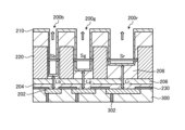
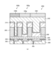
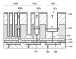
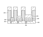
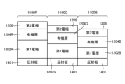
- Figure 5A is a cross-sectional view for explaining an example of the configuration of the light-emitting device according to the present embodiment
- Figure 5B is a plan view for explaining an example of the configuration of the light-emitting device according to the present embodiment.
- the display device (display device) 10 has a top emission type (top surface emission type), that is, a light emitting element 200 that emits light upward.
- a top emission type top surface emission type
- a plurality of light emitting elements 200r, 200g, 200b are arranged in a matrix in a predetermined region on the substrate 300.
- Each of the light emitting elements 200r, 200g, 200b emits, for example, red (R), green (G), and blue (B) light, respectively, and corresponds to the above-mentioned sub-pixels 100R, 100G, and 100B.
- each of the light emitting elements 200r, 200g, and 200b is the same as the sub-pixels 100R, 100G, and 100B that are treated as one unit during control.
- the display device 10 has a drive circuit board 300 provided with wiring, vias, and transistors, and a light-emitting element 200 consisting of a first electrode (anode electrode) 202, an organic EL film (light-emitting portion) 204, a second electrode (cathode electrode) 206, an optical adjustment layer 208, and a semi-transmissive reflective film 210.
- a light-emitting element 200 consisting of a first electrode (anode electrode) 202, an organic EL film (light-emitting portion) 204, a second electrode (cathode electrode) 206, an optical adjustment layer 208, and a semi-transmissive reflective film 210.
- the first electrode 202 and the semi-transmissive reflective film 210 function as the first and second reflective surfaces.
- the light-emitting elements 200r, 200g, and 200b according to this embodiment have a microcavity structure in which the distances Lb, Lg, and Lr between the first electrode 202 and the semi-transmissive reflective film 210 satisfy the above-mentioned formula (1) according to the color (wavelength) of the light emitted from the light-emitting element 200, as shown in FIG. 5A.
- the optical adjustment layer 208 of each light-emitting element 200 has a different film thickness according to the color (wavelength) of the light emitted from the light-emitting element 200. Therefore, according to this embodiment, the light from the organic EL film 204 can be efficiently extracted above each light-emitting element 200.
- a voltage is applied to the first electrode 202 through a via 302 provided in the drive circuit board 300.
- the optical adjustment layer 208 is formed from a transparent conductive material such as IZO (indium zinc oxide), so that the optical adjustment layer 208 is integrated with the second electrode 206 and can function as a single electrode.
- each light-emitting element 200 The layers that make up each light-emitting element 200 are described in detail below.
- the drive circuit substrate 300 can be made of a transparent material such as glass, or a semiconductor material such as silicon.
- the drive circuit for driving the light emitting element 200 is constructed by appropriately forming transistors, wiring, and the like on the above-mentioned various substrates 300.
- a first electrode 202 and an inter-pixel insulating portion 230, which will be described later, are provided on the drive circuit substrate 300.
- the first electrode 202 can be formed of a light-reflecting material such as aluminum (Al), an aluminum alloy, silver (Ag), a silver alloy, etc.
- the film thickness of the first electrode 202 is preferably, for example, 100 to 300 nm.
- the first electrode 202 may also be a multi-layer film, for example, having a configuration in which a transparent conductive layer and a light-reflecting layer are laminated. More specifically, the first electrode 202 may have a configuration in which an aluminum alloy layer is laminated as a first layer (light-reflecting layer) and a transparent conductive layer such as indium tin oxide (ITO) or indium zinc oxide (IZO) is laminated as a second layer (transparent conductive layer).
- ITO indium tin oxide
- IZO indium zinc oxide
- the first electrode 202 may also have a configuration in which an inorganic hole injection layer and a light reflecting layer are laminated together. More specifically, the first electrode 202 may have a configuration in which an aluminum alloy layer is used as the first layer (light reflecting layer) and an inorganic material layer such as titanium (Ti), titanium oxide (TiO), titanium nitride (TiN), molybdenum (Mo), molybdenum oxide ( MoO3 ), etc. is used as the second layer (inorganic hole injection layer).
- an aluminum alloy layer is used as the first layer (light reflecting layer) and an inorganic material layer such as titanium (Ti), titanium oxide (TiO), titanium nitride (TiN), molybdenum (Mo), molybdenum oxide ( MoO3 ), etc. is used as the second layer (inorganic hole injection layer).
- an inorganic material layer made of Ti, TiN, or the like may be provided as a base layer under the first electrode 202.
- the outer periphery of the first electrode 202 is covered with an inter-pixel insulating section 230, and the central region of the first electrode 202 exposed from the opening (pixel opening) of the inter-pixel insulating section 230 functions as an electrode.
- the inter-pixel insulating section 230 defines the light-emitting region by the pixel opening.
- the inter-pixel insulating section 230 can be formed, for example, from an inorganic insulating film such as silicon oxide (SiOx), silicon nitride (SiNx), or silicon oxynitride (SiON), or an organic insulating film such as a polyimide resin, an acrylic resin, or a novolac resin.
- an inorganic insulating film such as silicon oxide (SiOx), silicon nitride (SiNx), or silicon oxynitride (SiON), or an organic insulating film such as a polyimide resin, an acrylic resin, or a novolac resin.
- the organic EL film 204 is formed as a single, continuous layer across the plurality of light emitting elements 200 above the first electrode 202.
- the organic EL film 204 is In this embodiment, the organic EL film 204 is formed as a single layer that is shared by the plurality of light emitting elements 200r, 200g, and 200b.
- the optical adjustment layer 208 of each light emitting element 200 is formed in a different layer according to the color (wavelength) of the light emitted from the light emitting element 200.
- the light emitting element 200 according to this embodiment has an organic EL film 204 made of an organic material as a light emitting portion.
- the present embodiment is not limited to this, and the light emitting element 200 according to the present embodiment may have an EL film made of an inorganic material as a light emitting portion.
- the organic EL film 204 has three light-emitting layers of red, green, and blue, for example, laminated across all the light-emitting elements 200, that is, it has a structure of the White method that extracts white light.
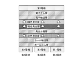
- the organic EL film 204 has a so-called 1-stack structure, in which, for example, a hole injection layer, a hole transport layer, a red light-emitting layer, a light-emitting separation layer, a blue light-emitting layer, a green light-emitting layer, and an electron transport layer are stacked in this order from bottom to top (see FIG. 8A).
- Each light-emitting layer may have a multi-layer structure in which different light-emitting materials that emit light of the same color are stacked. By stacking light-emitting materials with different properties and separating their functions, local deterioration within the light-emitting layer is suppressed, and a highly efficient, long-life element can be obtained. Details of variations in the configuration of the organic EL film 204 will be described later (FIGS. 8A to 8I). Below, a 1-stack structure will be described as an example of the organic EL film 204 according to this embodiment.
- the hole injection layer can be made of, for example, hexaazatriphenylene (HAT).
- the hole transport layer can be composed of, for example, ⁇ -NPD [N,N'-di(1-naphthalyl)-N,N'-diphenyl-[1,1'-biphenyl]-4,4'-diamine].
- the red light-emitting layer generates red light by applying an electric field, whereby some of the holes injected from the first electrode 202 through the hole injection layer and the hole transport layer and some of the electrons injected from the second electrode 206 through the electron transport layer are recombined.
- the red light-emitting layer contains, for example, at least one of a red light-emitting material, a hole transport material, an electron transport material, and a positive and negative charge transport material.
- the red light-emitting material may be fluorescent or phosphorescent.
- the red light-emitting layer may be composed of, for example, 4,4-bis(2,2-diphenylvinyl)biphenyl (DPVBi) mixed with 30% by weight of 2,6-bis[(4'-methoxydiphenylamino)styryl]-1,5-dicyanonaphthalene (BSN).
- DPVBi 4,4-bis(2,2-diphenylvinyl)biphenyl
- BSN 2,6-bis[(4'-methoxydiphenylamino)styryl]-1,5-dicyanonaphthalene
- the emission separation layer is a layer for adjusting the injection of carriers into the emission layers, and the light emission balance of each color is adjusted by injecting electrons and holes into each emission layer through the emission separation layer.
- the emission separation layer can be composed of, for example, a 4,4'-bis[N-(1-naphthyl)-N-phenyl-amino]biphenyl derivative.
- the blue light-emitting layer generates blue light by applying an electric field, whereby some of the holes injected from the first electrode 202 through the hole injection layer, hole transport layer, and light-emitting separation layer and some of the electrons injected from the second electrode 206 through the electron transport layer are recombined.
- the blue light-emitting layer contains, for example, at least one of a blue light-emitting material, a hole transport material, an electron transport material, and a bipolar charge transport material.
- the blue light-emitting material may be fluorescent or phosphorescent.
- the blue light-emitting layer may be composed of, for example, DPVBi mixed with 2.5% by weight of 4,4'-bis[2- ⁇ 4-(N,N-diphenylamino)phenyl ⁇ vinyl]biphenyl (DPAVBi).
- the green light-emitting layer contains, for example, at least one of a green light-emitting material, a hole transport material, an electron transport material, and a bipolar charge transport material.
- the green light-emitting material may be fluorescent or phosphorescent.
- the green light-emitting layer may be composed of, for example, DPVBi mixed with 5% by weight of coumarin 6.
- the electron transport layer may be made of, for example, BCP (2,9-dimethyl-4,7-diphenyl-1,10-phenanthroline), Alq3 (aluminum quinolinol), or Bphen (bathophenanthroline).
- the electron transport layer is made up of at least one layer, and may include an electron transport layer doped with an alkali metal or alkaline earth metal.
- the electron transport layer doped with an alkali metal or alkaline earth metal can be composed of a host material such as BCP (2,9-dimethyl-4,7-diphenyl-1,10-phenanthroline), Alq3 (aluminum quinolinol), or Bphen (bathophenanthroline), and a dopant material such as an alkali metal such as lithium (Li), sodium (Na), potassium (K), rubidium (Rb), or cesium (Cs), or an alkaline earth metal such as magnesium (Mg), calcium (Ca), strontium (Sr), or barium (Ba), doped to, for example, 0.5 to 15% by weight by co-evaporation.
- a host material such as BCP (2,9-dimethyl-4,7-diphenyl-1,10-phenanthroline), Alq3 (aluminum quinolinol), or Bphen (bathophenanthroline)
- a dopant material such as an alkali metal such as lithium (
- an electron injection layer may be provided between the electron transport layer and the second electrode 206.
- the electron injection layer is intended to increase electron injection from the cathode, and may be composed of an alkali metal or alkaline earth metal alone, a compound containing them, or a mixture containing them.
- the electron injection layer may be composed of lithium (Li), lithium fluoride (LiF), etc.
- a buffer layer may be provided between the electron transport layer and the second electrode 206.
- the buffer layer is intended to reduce process damage during the formation of the second electrode 206.
- the buffer layer may be composed of, for example, an alkali metal or alkaline earth metal such as Mg, magnesium silver alloy (MgAg), Ca, Li, LiF, lithium carbonate (Li 2 CO 3 ), Cs, cesium carbonate (Cs 2 CO 3 ), or a compound containing the same or a mixture containing the same.
- each layer constituting the organic EL film 204 is preferably, for example, 1 to 20 nm for the hole injection layer, 10 to 200 nm for the hole transport layer, 5 to 50 nm for the light emitting layer, and 10 to 200 nm for the electron transport layer. Furthermore, it is preferable that the thickness of the organic EL film 204 and each layer constituting it is set to a value that allows the optical thickness to be such that operation according to the wavelength (color) of the light emitted by each light emitting element 200 is possible.
- the second electrode 206 can be made of a transparent conductive material having good light transmittance and a small work function.
- the second electrode 206 can be made of indium zinc oxide (IZO), and the thickness thereof is preferably set to 10 to 500 nm.
- the second electrode 206 is formed as a single continuous layer across the plurality of light-emitting elements 200.
- the second electrode 206 is formed as a single layer shared by the plurality of light-emitting elements 200.
- the number of steps can be reduced by forming the second electrode 206 as a single layer across the plurality of light-emitting elements 200.
- the optical adjustment layer 208 is disposed above the organic EL film 204 and the second electrode 206 in order to adjust the optical distance L from the first reflection surface (the first electrode 202) to the second reflection surface (the semi-transmissive reflective film 210).
- the distances Lb, Lg, and Lr between the first electrode 202 and the semi-transmissive reflective film 210 determine the color of the light emitted from the light emitting element 200.
- the optical adjustment layer 208 of the element 200 has a different film thickness depending on the color (wavelength) of the light emitted from the light emitting element 200 .
- the resonance order m in formula (1) may be different for each light emitting element 200 that emits light of different colors.
- the optimal film thickness of the optical adjustment layer 208 of each light emitting element 200 is It can be changed by the wavelength ⁇ (the emission peak wavelength ⁇ of the light emitting element 200) and the resonance order m.
- the resonance order m is preferably 1 or 2.
- the film thickness of the optical adjustment layer 208 is preferably, for example, 1 to 500 nm. Furthermore, in this embodiment, it is preferable that the difference between the film thickness of the optical adjustment layer 208 of one type of light-emitting element 200 among the light-emitting elements 200r, 200g, 200b of the three colors of red, blue, and green and the film thickness of the optical adjustment layer 208 of the other type of light-emitting element 200 is, for example, 30 nm or more.
- the optical adjustment layer 208 is made of a transparent conductive material, and more specifically, can be made of an oxide such as IZO or ITO. In this embodiment, the optical adjustment layer 208 may be formed as a continuous film spanning multiple light-emitting elements 200.
- the semi-transmissive reflective film 210 is provided to enhance the effect of the microcavity structure, and is made of a semi-transmissive reflective material made of a metal having good light transmittance and light reflectance.
- the semi-transmissive reflective film 210 is provided above the optical adjustment layer 208.
- the semi-transmissive reflective film 210 can be made of Ag, gold (Au), copper (Cu), Al, Mg, or an alloy thereof.
- the alloy can be, for example, a magnesium silver alloy ( Examples of the alloy include silver alloys such as palladium-copper-silver alloy (AgPdCu(APC)), and Ag alloys such as palladium-copper-silver alloy (AgPdCu(APC)).
- silver alloys such as palladium-copper-silver alloy (AgPdCu(APC)
- Ag alloys such as palladium-copper-silver alloy (AgPdCu(APC)).
- the semi-transmissive reflective film 210 may be a multi-layer film that functions as an electrode together with the second electrode 206 and the optical adjustment layer 208.
- the semi-transmissive reflective film 210 may be, for example, a first layer made of a metal layer of Ca, Ba, Li, LiF, Cs, indium (In), Mg, Ag, or an alloy thereof, and a second layer made of a metal layer of Mg, Ag, or an alloy thereof.
- the multi-layer film of the semi-transmissive reflective film 210 may be made of the same material, for example, the first layer and the second layer made of an alloy metal layer of Mg and Ag, and the concentrations of the metals contained in these layers are different. More specifically, in this embodiment, for example, the Ag concentration of the first layer (lower layer) is made low and the Ag concentration of the second layer (upper layer) is made high. In this way, it is possible to increase the electron injection property while increasing the light extraction efficiency.
- the semi-transmissive reflective film 210 may be made of a dielectric multilayer film.
- the dielectric multilayer film is made of transparent material layers, and in order to obtain a half-mirror function, it is preferable that the refractive index difference with the second electrode 206 is 0.1 or more.
- the dielectric can be made of a material containing, for example, an oxide, a nitride, a sulfide, a carbonate, a fluoride, or an organic compound.
- the thickness of the semi-transmissive reflective film 210 is preferably, for example, 3 to 20 nm. Furthermore, in this embodiment, the semi-transmissive reflective film 210 can be formed as a continuous film on the optical adjustment layer 208 and the element isolation layer 220 described later, across the multiple light-emitting elements 200. In this embodiment, as described later, unevenness is formed on the light-emitting elements 200 and between the light-emitting elements 200 due to the element isolation layer 220. Since the semi-transmissive reflective film 210 is formed on this unevenness, the semi-transmissive reflective film 210 becomes redundant and can function as a lower resistance electrode together with the second electrode 206 and the optical adjustment layer 208. As a result, even if the display device 10 is made larger, the voltage drop caused by the resistance of the electrodes can be suppressed, making it possible to uniform the brightness within the surface of the display device 10.
- each light emitting element 200 is separated from the others by an element isolation layer 220 provided so as to surround the region (element region) in which the light emitting element 200 is located. Furthermore, in this embodiment, the size (width) of the opening provided in the element isolation layer 220, which is the element region surrounded by the element isolation layer 220, varies depending on the color (wavelength) of light emitted from the light emitting element 200.
- the above-mentioned optical adjustment layer 208 is provided so as to be embedded in the element region surrounded by the element isolation layer 220.
- the surface of the element isolation layer 220 is covered with the optical adjustment layer 208 and the semi-transmissive reflective film 210.
- the thickness of the element isolation layer 220 is preferably, for example, 0.5 to 5 ⁇ m.
- the element isolation layer 220 can be formed from an inorganic material, an organic material, a metal material, or the like. More specifically, the element isolation layer 220 can be formed from, for example, nitrides, oxides, oxynitrides, such as SiOx, SiNx, SiON, aluminum oxide (AlOx), titanium oxide (TiOx), and niobium oxide (NbO), and may further be formed from fluorides, organic compounds, or the like.
- the size (width) of the opening provided in the element isolation layer 220 which is the element region surrounded by the element isolation layer 220, depending on the color (wavelength) of light emitted from the light emitting element 200, it is possible to optimize the film thickness of the optical adjustment layer 208 of each light emitting element 200 while simultaneously forming the optical adjustment layer 208 of each light emitting element 200 that emits light of different colors.
- the area of the element region (opening) surrounded by the element isolation layer 220 of the light-emitting element (first light-emitting element) 200r is made larger than the area of the element region surrounded by the element isolation layer 220 of the light-emitting element (second light-emitting element) 200g. Also, in this embodiment, the area of the element region surrounded by the element isolation layer 220 of the light-emitting element (second light-emitting element) 200g is made larger than the area of the element region surrounded by the element isolation layer 220 of the light-emitting element (third light-emitting element) 200b.
- the spacing Sr between the pair of element isolation layers 220 that sandwich the light-emitting element (first light-emitting element) 200r is made larger than the spacing Sg between the pair of element isolation layers 220 that sandwich the light-emitting element (second light-emitting element) 200g.
- the spacing Sg between the pair of element isolation layers 220 sandwiching the light emitting element (second light emitting element) 200g is made wider than the spacing Sb between the pair of element isolation layers 220 sandwiching the light emitting element (third light emitting element) 200b.
- the spacing S between the pair of element isolation layers 220 sandwiching each light emitting element 200 is preferably, for example, 5 ⁇ m or less.
- the difference between the spacing S between the pair of element isolation layers 220 sandwiching one type of light emitting element 200 among the three light emitting elements 200r, 200g, and 200b of red, blue, and green and the spacing S between the pair of element isolation layers 220 sandwiching the other type of light emitting element 200 is preferably, for example, 0.5 ⁇ m or more.
- the optical adjustment layer 208 of each light-emitting element 200 that emits light of different colors is formed collectively, while the film thickness of the optical adjustment layer 208 of the light-emitting element (first light-emitting element) 200r can be easily made thicker than the film thickness of the optical adjustment layer 208 of the light-emitting element (second light-emitting element) 200g. Furthermore, according to this embodiment, the film thickness of the optical adjustment layer 208 of the light-emitting element (second light-emitting element) 200g can be easily made thicker than the film thickness of the optical adjustment layer 208 of the light-emitting element (third light-emitting element) 200b.
- the film thickness of the optical adjustment layer 208 of each light-emitting element 200 can be easily optimized by changing the area of the opening (the spacing of the element isolation layer 220) provided in the element isolation layer 220, which is the element region surrounded by the element isolation layer 220, and therefore it is possible to form a microcavity structure with high accuracy.
- the light extraction efficiency can be improved by the resonance of light due to the optimized microcavity structure.
- unevenness is formed on the light-emitting elements 200 and between the light-emitting elements 200 by the element isolation layer 220.
- the penetration length of the moisture that progresses along the surface of the element isolation layer 220 and the semi-transmissive reflective film 210 becomes longer due to the uneven shape, and the delay in the penetration improves the reliability of the display device 10.
- the light-emitting element 200 may be covered with a protective film (not shown), and a sealing material layer, an opposing substrate, etc. may be provided on the protective film.
- the light-emitting regions of the three light-emitting elements 200r, 200g, 200b of red, blue, and green colors exposed from the opening (element region) of the element isolation layer 220 have a rectangular shape and differ in area.
- the area of the light-emitting region of the light-emitting element (first light-emitting element) 200r is larger than the area of the light-emitting region of the light-emitting element (second light-emitting element) 200g.
- the area of the light-emitting region of the light-emitting element (second light-emitting element) 200g is larger than the area of the light-emitting region of the light-emitting element (third light-emitting element) 200b.
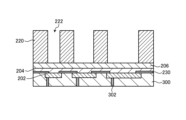
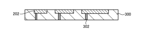
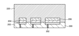
- Fig. 6A to Fig. 6D are explanatory views for explaining the method for manufacturing the light-emitting device 200 of this embodiment, and correspond to the cross-sectional view of Fig. 5A.
- transistors and the like are appropriately formed in wells provided in a substrate 300 made of a semiconductor material such as silicon.
- a wiring layer required for driving the light-emitting element 200 is formed.
- the wiring (not shown) included in the wiring layer can be formed by lithography using a material such as Al.
- the vias 302 included in the wiring layer can be formed using a material such as tungsten (W).
- a first electrode 202 is formed on the substrate 300.
- the first electrode 202 can be formed by forming an Al alloy by sputtering and patterning it.
- a SiNx film is formed as an insulating material layer constituting the inter-pixel insulating section 230 on the entire surface including the first electrode 202. Furthermore, the insulating material layer is patterned using a patterning technique such as lithography or etching to expose a part of the upper surface of the first electrode 202. In this way, the configuration shown in FIG. 6A can be obtained.
- a hole injection layer, a hole transport layer, a red light emitting layer, a light emitting separation layer, a blue light emitting layer, a green light emitting layer, an electron transport layer, and an electron injection layer are laminated in this order on the first electrode (first reflecting surface) 202 as the organic EL film (light emitting portion) 204.
- the organic EL film 204 can be formed by using a vapor deposition method.
- IZO is laminated over the entire surface as the second electrode 206 by a sputtering method.
- a SiN film is formed over the entire surface as the element isolation layer 220 on the second electrode 206 by a CVD method. In this manner, the configuration shown in FIG. 6B can be obtained.
- the SiN film is processed, for example, by dry etching, to leave the SiN film so as to surround the region (element region) where the light emitting element 200 is formed, thereby forming an opening 222 surrounding the element region.
- the SiN film is processed so that the area of the element region surrounded by the SiN film varies depending on the color of light emitted by the light emitting element 200. In this way, an element isolation layer 220 as shown in FIG. 6C can be obtained.
- IZO is formed over the entire surface by sputtering as the optical adjustment layer 208.
- the area of the element region surrounded by the element isolation layer 220 varies depending on the color of light emitted by the light emitting element 200, and therefore the film thickness of the optical adjustment layer 208 embedded in the element region varies depending on the color of light emitted by the light emitting element 200. In this way, the element isolation layer 220 as shown in FIG. 6D can be obtained.
- a semi-transmissive reflective film (second reflective surface) 210 for example an Ag alloy film, is formed over the entire surface by sputtering or vapor deposition. In this way, a light-emitting element 200 as shown in FIG. 5A can be obtained.
- an inorganic protective film (not shown) made of, for example, SiON is formed over the entire surface by CVD. Furthermore, an organic protective film (not shown) made of, for example, acrylic resin is formed over the entire surface by screen printing. Next, an inorganic protective film (not shown) made of, for example, SiON is formed over the entire surface by CVD.
- the display device 10 can be manufactured.
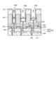
- Fig. 7 is a cross-sectional view for explaining an example of a configuration of a main part of a light-emitting element 200 according to a first modified example of the present embodiment, and shows a cross section of a first electrode 202 and an inter-pixel insulating portion 230.
- this modification variations of the first electrode 202 and the inter-pixel insulating portion 230 will be described.
- FIG. 7(a) shows a cross section of the first electrode 202 and inter-pixel insulating portion 230 of the first embodiment described above.
- the outer periphery of the first electrode 202 is covered with the inter-pixel insulating portion 230, and the center of the first electrode 202 exposed from the opening (pixel opening) of the inter-pixel insulating portion 230 functions as an electrode.
- the inter-pixel insulating portion 230 defines the light-emitting region by the pixel opening.
- the organic EL film 204 in this embodiment is formed over the entire surface across multiple light-emitting elements 200, and the inter-pixel insulating portion 230 can suppress current leakage (lateral leakage) between adjacent light-emitting elements 200.
- the end of the first electrode 202 may have an inclined surface or a rounded shape. In this way, diffuse reflection of light caused by unintended emission at the end of the first electrode 202 can be suppressed.
- a recessed portion may be formed in the first electrode 202.
- the recessed portion By forming the recessed portion in this manner, it is possible to suppress a decrease in luminous efficiency and abnormal luminescence caused by current leakage in the organic EL film 204 located at the edge of the pixel opening.
- the end of the inter-pixel insulating portion 230 is sloped or the corners are rounded, thereby preventing the organic EL film 204 from becoming locally thin, and thus preventing the above-mentioned current leakage.
- the inter-pixel insulating section 230 by forming the inter-pixel insulating section 230 into an inverted taper shape or an overhanging shape and depositing the organic EL film 204, the hole injection layer, hole transport layer, and charge generation layer located in the lower layer of the organic EL film 204 are thinned or separated by the inverted taper shape or overhanging shape of the inter-pixel insulating section 230. As a result, current leakage between multiple light-emitting elements 200 can be suppressed.
- the eaves-shaped portion of the inter-pixel insulating portion 230 may be multi-staged, and as shown in FIG. 7(i), multi-stage eaves portions may be formed on the inclined surface of the inter-pixel insulating portion 230 with their tips positioned at different positions.
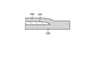
- a groove 234 may be provided between the light-emitting elements 200. This also makes it possible to suppress current leakage between multiple light-emitting elements 200. Also, as shown in FIG. 7(k), the groove 234 may be provided with a canopy.
- inter-pixel electrodes 232 may be formed between the multiple light-emitting elements 200.
- the inter-pixel electrodes 232 can draw in leakage current, thereby preventing a decrease in light-emitting efficiency and abnormal light emission.
- Figures 8A to 8I are cross-sectional views for explaining an example of the configuration of a light-emitting element 200 according to the second modification of the present embodiment, and more specifically, show a cross section of the layer structure of an organic EL film 204. In this modification, variations in the organic EL film 204 will be described.
- FIG. 8A shows a cross section of the organic EL film 204 of the first embodiment described above.
- the organic EL film 204 has a so-called one-stack structure, in which, for example, a hole injection layer, a hole transport layer, a red light-emitting layer, a light-emitting separation layer, a blue light-emitting layer, a green light-emitting layer, and an electron transport layer are stacked in this order from the bottom up.
- FIG. 8B there may be two light-emitting separation layers between the light-emitting layers.
- the light-emitting layer may be composed of two color layers, a blue light-emitting layer and a yellow light-emitting layer.
- the organic EL film 204 may have a so-called 2-stack structure in which a hole injection layer, a hole transport layer, a blue light-emitting layer, an electron transport layer, a charge generation layer, a hole injection layer, a hole transport layer, a yellow light-emitting layer, and an electron transport layer are stacked in this order from the bottom up.
- the light-emitting layers may be composed of three colors, red, green, and blue.
- a light-emitting separation layer may be provided between the light-emitting layers.
- the red, green, and blue light-emitting layers may be partially painted differently.
- the light-emitting layers may be painted to include either an electron blocking layer or a hole blocking layer, or both.
- the green light-emitting layer and the red light-emitting layer may be partially painted differently, and then the blue light-emitting layer may be laminated as a common layer.
- each light-emitting layer may be constructed by laminating layers of different materials of the same color.
- functions can be separated. This prevents localized deterioration within the light-emitting layer, resulting in a highly efficient, long-life element.
- FIGS. 9A and 9B are cross-sectional views for explaining an example of a configuration of a main part of the light-emitting element 200 according to the third modification of this embodiment, and in detail show a cross section of the element isolation layer 220.
- variations in the element isolation layer 220 will be described.
- the optical adjustment layer 208 by changing the spacing and shape of the element isolation layer 220, it is possible to collectively form the optical adjustment layer 208 having a film thickness according to the color of light emitted by the light-emitting element 200.
- FIG. 9A(a) shows a cross section of the element isolation layer 220 of the first embodiment described above.
- the cross section of the element isolation layer 220 is rectangular.
- the cross section of the element isolation layer 220 may be tapered, and as shown in FIG. 9A(c), the cross section of the element isolation layer 220 may be curved. Furthermore, as shown in FIG. 9A(d), the cross section of the element isolation layer 220 may be multi-stepped, as shown in FIG. 9A(e), the cross section of the element isolation layer 220 may be eaves-shaped, and as shown in FIG. 9A(f), the cross section of the element isolation layer 220 may be rounded.
- multiple element isolation layers 220 may be provided between the light-emitting elements 200.
- the inside of the element isolation layer 220 may be provided with a light guide portion 226 made of a low refractive index material.
- the low refractive index material may be, for example, a transparent material such as SiNx, SiOx , LiF, magnesium fluoride (MgF), SiON, an organic material used in the organic EL film 204, other organic compounds, a low refractive index resin, or the like.
- the light guide portion 226 functions as a reflective surface and can guide light from the organic EL film 204 upward.
- the light guide portion 226 may also be formed from a metal material including Al, Ti, Cu, W, Ag, Mg, or the like. In this way, the light extraction efficiency is further improved and color mixing is further suppressed.
- an air gap 228 may be provided in the element isolation layer 220.
- the light guide 226 can function as a reflective surface and guide the light from the organic EL film 204 upward. As a result, the light extraction efficiency is improved and color mixing between adjacent light emitting elements 200 can be suppressed.
- Fig. 10A is a cross-sectional view for explaining an example of the configuration of the light-emitting element 200 according to the fourth modification of the present embodiment.
- Fig. 10B is a plan view for explaining an example of the configuration of the light-emitting element 200 according to the fourth modification of the present embodiment.
- the light-emitting element 200 further has a reflector 312 provided below the first electrode 202.
- the light-emitting element 200 has a first electrode (anode) 202, an organic EL film (light-emitting portion) 204, a second electrode (cathode) 206, an optical adjustment layer 208, a semi-transmissive reflective film 210, an insulating film 320, and a reflector 312.
- the reflector 312 is provided below the first electrode 202 via the insulating film 320.
- the reflector 312 and the semi-transmissive reflective film 210 function as a first and second reflective surface, and have a microcavity structure in which the distances Lb, Lg, and Lr between the reflector 312 and the semi-transmissive reflective film 210 satisfy the above-mentioned formula (1) for the color (wavelength) of light emitted from the light-emitting element 200. Therefore, according to this modified example, light from the organic EL film 204 can be efficiently extracted above each light-emitting element 200.
- the spacing Sb between the pair of element isolation layers 220 that sandwich the light-emitting element (third light-emitting element) 200b is narrower than the spacing Sg between the pair of element isolation layers 220 that sandwich the light-emitting element (second light-emitting element) 200g. Therefore, although the distance from the reflector 312 to the second electrode 206 is the same in the light-emitting element 200b and the light-emitting element 200g, the film thickness of the optical adjustment layer 208 is different, and the film thickness of the optical adjustment layer 208 of the light-emitting element 200b is thinner than the film thickness of the optical adjustment layer 208 of the light-emitting element 200g.
- the spacing Sr between the pair of element isolation layers 220 sandwiching the light-emitting element (first light-emitting element) 200r is equal to the spacing Sg between the pair of element isolation layers 220 sandwiching the light-emitting element (second light-emitting element) 200g. Therefore, the light-emitting element 200r and the light-emitting element 200g have the same film thickness of the optical adjustment layer 208 of the light-emitting element 200r and the film thickness of the optical adjustment layer 208 of the light-emitting element 200g, but the distance from the reflector 312 to the second electrode 206 is different.
- the film thickness of the insulating film 320 under the first electrode 202 is made thicker in the light-emitting element 200r, thereby making the distance Lr longer than the distance Lg.
- the optical path L can be adjusted by the film thickness of the insulating film 320, so that adjustments can be made more precisely according to the wavelength of light. This makes it possible to form a microcavity structure with precision, and the light extraction efficiency can be further improved. That is, in this modified example, by using the reflector 312 and the insulating film 320, it is possible to form a microcavity structure with precision, while increasing the degree of freedom in the shape and size of the light-emitting element 200 in plan view.
- the optical distance L was adjusted by changing the film thickness of the insulating film 320 under the first electrode 202, but in this modified example, the method is not limited to this, and the optical distance L may be adjusted by changing the film thickness of the first electrode 202, for example.
- the insulating film 320 may be a multi-layer film composed of insulating films 320a and 320b made of different materials.
- the reflector 312 may be formed, for example, from a metal such as Al, Ag, or Cu, or an alloy containing these as its main components.
- the first electrode 202 may also be electrically connected to the reflector 312.
- the first electrode 202 may be connected to a driving circuit of the substrate 300 via the reflector 312.
- the first electrode 202 and the reflector 312 may be connected by contact portions 252 arranged around the first electrode 202 (near the light-emitting element 200 in the effective pixel area), and one or more contact portions 252 may be provided for one first electrode 202.
- the reflector 312 and the first electrode 202 may have different dimensions, and may be arranged so that at least a portion of them overlap each other.
- the reflector 312 is not limited to being separated for each light-emitting element 200, but may be provided as a single, continuous layer so as to be common to multiple light-emitting elements 200.
- FIG. 11A and Fig. 11B are cross-sectional views for explaining an example of the configuration of a light-emitting element 200 according to the fifth modified example of the present embodiment.
- a contact portion connected to the second electrode 206 will be described.
- the second electrode 206, the optical adjustment layer 208, and the semi-transmissive reflective film 210 on the organic EL film 204 are electrically connected to the potential supply wiring 304 through the contact hole 306 in the cathode contact portion 252 arranged in the outer periphery 250 of the display area in which the multiple light-emitting elements 200 are arranged in a matrix.
- the optical adjustment layer 208 and the semi-transmissive reflective film 210 may be connected to the second electrode 206a located around the light-emitting element 200 in the effective pixel region.
- a protective film 240 can be disposed between the second electrode 206 of the light-emitting element 200 in the effective pixel region and the optical adjustment layer 208.
- the protective film 240 is formed on the second electrode 206, thereby making it possible to suppress damage to the second electrode 206 during processing of the element isolation layer 220. As a result, this modification makes it possible to improve the reliability of the display device 10.
- Fig. 12A and Fig. 12B are cross-sectional views for explaining an example of the configuration of a light-emitting element 200 according to the sixth modification of the present embodiment.
- a protective film that covers the entire light-emitting element 200 will be described.
- the protective film that covers the entire light-emitting element 200 is intended to prevent moisture from entering the organic EL film 204, and is formed using a material with low transparency and water permeability.
- materials for the protective film include SiNx, SiOx, AlOx, TiOx, or combinations of these.
- the thickness of the protective film is preferably, for example, 0.5 to 8 ⁇ m.
- the protective film may be a laminated film. Specifically, as shown in FIG. 12A, the protective film may be composed of three layers: a first inorganic protective film 330, an organic protective film 332, and a second inorganic protective film 334.
- the first inorganic protective film 330 and the second inorganic protective film 334 may be made of SiON or the like.
- the organic protective film 332 may be made of acrylic resin or the like.
- the first inorganic protective film 330 and the second inorganic protective film 334 are connected at the outer periphery of the display area.
- an opposing substrate may be provided on the protective film. After the protective film is formed, the opposing substrate is sealed by applying a UV-curable resin or a thermosetting resin and bonding it together.
- the opposing substrate may be provided with a light-shielding film as a color filter or black matrix, which enhances the color purity of the light generated by the light-emitting elements 200 and extracts it, and absorbs external light reflected by the wiring between the light-emitting elements 200, improving contrast.
- Fig. 13A and Fig. 13B are cross-sectional views for explaining an example of a configuration of a main part of a light-emitting device 200 according to the seventh modification of the present embodiment.
- OCCF on-chip color filter
- an on-chip color filter 336 may be provided between the light-emitting element 200 and the opposing substrate (not shown).
- a blue color filter 336b may be provided on the protective film 342 covering the light-emitting element 200b
- a blue color filter 336g may be provided on the protective film 342 covering the light-emitting element 200g
- a red color filter 336r may be provided on the protective film 342 covering the light-emitting element 200r.
- this modified example is not limited to providing the color filter 336 on all the light-emitting elements 200, and may be provided only on some of the light-emitting elements 200.
- a partition 338 may be provided between the color filters 336.
- the partition 338 is made of a light-transmitting material and is disposed between the color filters 336 to suppress color mixing between adjacent light-emitting elements 200.
- adjacent color filters 336 may be overlapped with each other to function as a light-shielding film. As shown in FIG.
- the thickness of the color filter 336 of one type of light-emitting element 200 among the light-emitting elements 200r, 200g, and 200b of three colors, red, blue, and green, may be thinner than the partition 338, and the thickness of the color filter 336 of the other type of light-emitting element 200 may be thicker than the partition 338.
- the light-emitting element 200 has a microcavity structure, so that the color purity is high, and therefore the color filter 336 can be made thin. Therefore, in this modified example, by thinning at least some of the color filters, the light loss in the color filter 336 can be reduced and the light extraction efficiency can be increased.
- color filters 336b, 336g, and 336r of different colors may be stacked on the periphery of the display area to function as a peripheral light-shielding film 340.
- the peripheral light-shielding film 340 can be formed simultaneously with the formation of the color filter 336, so that a light-shielding function can be added without increasing the number of processes, and adverse optical effects can be reduced.
- optical components such as the color filter 336 may be encapsulated in a protective film (not shown).
- a protective film it is preferable to form an inorganic protective film (not shown) so as to cover the top and bottom of the color filter 336, etc., and to connect these inorganic protective films at the outer periphery of the display area.
- an inorganic protective film not shown
- the reliability of the display device 10 can be improved.
- the color filter 336 may be arranged with an offset within the plane of the display area relative to the center of the pixel aperture. By shifting the relative positional relationship from the center to the periphery of the display area, it is possible to improve the viewing angle characteristics. This will be described in more detail later.
- FIG. 14A to Fig. 14C are cross-sectional views for explaining an example of the configuration of a light-emitting device 200 according to the eighth modification of the present embodiment.
- OCL on-chip lens
- an on-chip lens 350 may be provided above the light-emitting element 200.
- the on-chip lens 350 it is possible to increase the light extraction efficiency.
- this modification is not limited to providing the on-chip lens 350 on all the light-emitting elements 200, and the on-chip lens 350 may be provided on only some of the light-emitting elements 200.
- the width and height of the on-chip lens 350 may differ depending on the size of the light-emitting element 200.
- optical components such as the on-chip lens 350 may be encapsulated in a protective film (not shown).
- a protective film (not shown).
- inorganic protective films (not shown) so as to cover the top and bottom of the on-chip lens 350, etc., and to connect these inorganic protective films at the outer periphery of the display area.
- the on-chip lens 350 may also be arranged with an offset within the plane of the display area relative to the center of the pixel aperture. By shifting the relative positional relationship from the center to the periphery of the display area, it is possible to improve the viewing angle characteristics. This will be described in more detail later.
- Fig. 15 is a plan view for explaining an example of a configuration of a light-emitting element 200 according to the ninth modified example of the present embodiment. In this modification, variations in the layout of the light-emitting element 200 in a plan view will be described.
- the light emitting elements 200 may be arranged in a stripe pattern, as shown in Figs. 15(d) and (e), the light emitting elements 200 may be arranged in a square arrangement (each light emitting element 200 is arranged at the vertices of a rectangle), as shown in Figs. 15(f) and (g), the light emitting elements 200 may be arranged in a delta arrangement (each light emitting element 200 is arranged at the vertices of a triangle). Any color may be assigned to each light emitting element 200. As shown in Fig.
- the width of the inter-pixel insulating portion 230 may be adjusted so that the area of the pixel opening (light emitting region) of each light emitting element 200 is the same. As shown in Fig. 15(c), multiple light emitting elements 200 may be arranged in a region (element region) surrounded by one element isolation layer 220.
- Fig. 16A and Fig. 16C are cross-sectional views for explaining an example of the configuration of a light-emitting element 200 according to the modification 10 of this embodiment
- Fig. 16B is a plan view for explaining an example of the configuration of a light-emitting element 200 according to the modification 10 of this embodiment.
- this modification a form in which one sub-pixel 100 is divided into a plurality of light-emitting elements 200 will be described.
- sub-pixel 100B is divided into nine parts by inter-pixel insulation section 230 and has nine light-emitting elements 200b
- sub-pixel 100G is divided into four parts by inter-pixel insulation section 230 and has four light-emitting elements 200g
- sub-pixel 100R is not divided and has one light-emitting element 200r. That is, in this modified example, sub-pixels (first sub-pixel, second sub-pixel) 100G, 100B, which are treated as one unit during control, have multiple light-emitting elements 200g, 200b.
- an element isolation layer 220 is provided between each light-emitting element 200, and the spacing Sr between the pair of element isolation layers 220 that sandwich the light-emitting element (first light-emitting element) 200r is wider than the spacing Sg between the pair of element isolation layers 220 that sandwich the light-emitting element (second light-emitting element) 200g.
- the spacing Sg between the pair of element isolation layers 220 that sandwich the light-emitting element (second light-emitting element) 200g is wider than the spacing Sb between the pair of element isolation layers 220 that sandwich the light-emitting element (third light-emitting element) 200b.
- the optical adjustment layer 208 of each light-emitting element 200 that emits light of different colors is formed collectively, and the film thickness of the optical adjustment layer 208 of the light-emitting element (first light-emitting element) 200r can be easily made thicker than the film thickness of the optical adjustment layer 208 of the light-emitting element (second light-emitting element) 200g. Furthermore, according to this modified example, the film thickness of the optical adjustment layer 208 of the light-emitting element (second light-emitting element) 200g can be easily made thicker than the film thickness of the optical adjustment layer 208 of the light-emitting element (third light-emitting element) 200b.
- the film thickness of the optical adjustment layer 208 of each light-emitting element 200 can be easily optimized, making it possible to form a microcavity structure with high accuracy.
- the light extraction efficiency can be improved by the resonance of light due to the optimized microcavity structure.
- the subpixels 100 are divided, it is possible to improve the light extraction efficiency without compromising the definition or light-emitting area.
- one or more light-emitting elements 200 in each subpixel 100 share one first electrode 202, and multiple subpixels 100 share the organic EL film 204 and the second electrode 206.
- the on-chip lens 350 may be formed for each light-emitting element 200, not for each sub-pixel 100. In this way, the light extraction efficiency can be further improved. Note that in this modification, the on-chip lens 350 is not limited to being provided for each light-emitting element 200, and may be provided for each sub-pixel 100.
- FIG. 17 is a cross-sectional view for describing an example of the configuration of the light-emitting element 200 according to the present embodiment.
- the organic EL film 204 and the second electrode 206 are separated as separate layers for each light-emitting element 200. Furthermore, the separated second electrodes 206 are electrically connected to each other by the optical adjustment layer 208 and the semi-transmissive reflective film 210.
- the hole injection layer and the charge generation layer which are likely to cause leakage between adjacent light-emitting elements 200, are separated between the light-emitting elements 200, so that leakage between the light-emitting elements 200 can be suppressed.
- the plan view of the light-emitting element 200 according to this embodiment is the same as that of the first embodiment described using FIG. 5B, and therefore the description thereof will be omitted here.
- the first electrode 202 and the semi-transmissive reflective film 210 also function as the first and second reflective surfaces.
- the light-emitting elements 200r, 200g, and 200b according to this embodiment have a microcavity structure in which the distances Lb, Lg, and Lr between the first electrode 202 and the semi-transmissive reflective film 210 satisfy the above-mentioned formula (1) according to the color (wavelength) of the light emitted from the light-emitting element 200, as shown in FIG. 17.
- an element isolation layer 220 is provided between each light emitting element 200.
- the spacing Sr between the pair of element isolation layers 220 sandwiching the light emitting element (first light emitting element) 200r is made wider than the spacing Sg between the pair of element isolation layers 220 sandwiching the light emitting element (second light emitting element) 200g.
- the spacing Sg between the pair of element isolation layers 220 sandwiching the light emitting element (second light emitting element) 200g is made wider than the spacing Sb between the pair of element isolation layers 220 sandwiching the light emitting element (third light emitting element) 200b.
- the optical adjustment layer 208 of each light-emitting element 200 that emits light of different colors is formed collectively, and the film thickness of the optical adjustment layer 208 of the light-emitting element (first light-emitting element) 200r can be easily made thicker than the film thickness of the optical adjustment layer 208 of the light-emitting element (second light-emitting element) 200g. Furthermore, according to this embodiment, the film thickness of the optical adjustment layer 208 of the light-emitting element (second light-emitting element) 200g can be easily made thicker than the film thickness of the optical adjustment layer 208 of the light-emitting element (third light-emitting element) 200b.
- the film thickness of the optical adjustment layer 208 of each light-emitting element 200 can be easily optimized by changing the area of the opening (the spacing of the element isolation layer 220) provided in the element isolation layer 220, which is the element region surrounded by the element isolation layer 220, and therefore it is possible to form a microcavity structure with high accuracy.
- the light extraction efficiency can be improved by the resonance of light due to the optimized microcavity structure.
- the organic EL film 204 may be formed to be narrower than the width of the first electrode 202, and may also be formed to be narrower than the width of the second electrode 206. Also, in this embodiment, in the cross-sectional view of FIG. 17, the organic EL film 204 and the second electrode 206 may have tapered end faces.
- a sidewall protective film (not shown) containing the constituent elements of the base may be formed on the end surface of the organic EL film 204, thereby improving reliability.
- a sidewall protective film (not shown) made of an oxide containing the constituent elements of the first electrode 202, such as AlOx, may be formed on the end surface of the first electrode 202. In this way, the insulating effect between the multiple light-emitting elements 200 can be improved, making it possible to further narrow the pitch and obtain high-definition elements.
- the sidewall reflection area at the end face of the light emitting element 200 can be increased, and the light extraction efficiency can be further improved.
- the low refractive index material include transparent materials such as SiNx, SiO2, LiF, MgF, and SiON.
- the low refractive index material may also be a porous film (a film with low film density). For example, by using SiOx as a porous film, a film with an even lower refractive index, having a refractive index of 1.4 or less, can be obtained.
- the low refractive index material may also be composed of the organic material used in the organic EL film 204, other organic compounds, or low refractive index resins.
- the low refractive index film may also be formed as a low refractive index portion within the sidewall protective film. Furthermore, such a low refractive index portion within the sidewall protective film may be an air gap.
- Fig. 18A to Fig. 18F are explanatory views for explaining the method for manufacturing the light-emitting element 200 of this embodiment, and correspond to the cross-sectional views of Fig. 17.
- transistors and the like are appropriately formed in wells provided in a substrate 300 made of a semiconductor material such as silicon.
- a wiring layer required for driving the light-emitting element 200 is formed.
- a first electrode 202 is formed on the substrate 300. In this manner, a configuration such as that shown in FIG. 18A can be obtained.
- a hole injection layer, a hole transport layer, a red light emitting layer, a light emitting separation layer, a blue light emitting layer, a green light emitting layer, an electron transport layer, and an electron injection layer are laminated in this order on the first electrode (first reflecting surface) 202 as the organic EL film (light emitting portion) 204.
- IZO is laminated over the entire surface as the second electrode 206 by a sputtering method.
- a SiN film is formed over the entire surface as the protective film 224 on the second electrode 206 by a CVD method. In this manner, the configuration shown in FIG. 18B can be obtained.
- each layer is processed so that the organic EL film 204, the second electrode 206, and the protective film 224 are completely separated. In this way, the shape shown in Figure 18C can be obtained.
- an element isolation layer 220 is formed over the entire surface by CVD, for example, using SiN, so as to cover the processed end surface of the processed organic EL film 204. In this way, the shape shown in Figure 18D can be obtained.
- the SiN film is processed, for example, by dry etching, and the SiN film is left so as to surround the region (element region) where the light emitting element 200 is formed, thereby forming an opening 222 surrounding the element region.
- the SiN film is processed so that the area of the element region surrounded by the SiN film varies depending on the color of light emitted by the light emitting element 200. In this way, an element isolation layer 220 as shown in FIG. 18E can be obtained.
- the optical adjustment layer 208 is formed over the entire surface.
- the area of the element region surrounded by the element isolation layer 220 varies depending on the color of light emitted by the light emitting element 200, and therefore the film thickness of the optical adjustment layer 208 embedded in the element region varies depending on the color of light emitted by the light emitting element 200.
- the element isolation layer 220 as shown in FIG. 18F can be obtained.
- a semi-transmissive reflective film (second reflective surface) 210 is formed over the entire surface. In this manner, a light-emitting element 200 as shown in FIG. 17 can be obtained.
- Fig. 19 is a plan view for explaining an example of a configuration of a main part of a light emitting device 200 according to a first modified example of this embodiment, and in detail shows the shape of the light emitting device 200 in a plan view. In this modification, variations in the shape of the light emitting device 200 in a plan view will be described.
- the shape of the light emitting element 200 in plan view (specifically, the shape of the light emitting region of the light emitting element 200 exposed from the opening (element region) of the element isolation layer 220) may be rectangular, circular, polygonal, or donut-shaped with the center removed. Also, as shown in FIGS. 19(g) to (i), the shape of the light emitting element 200 in plan view may be curved, for example, S-shaped, U-shaped, or L-shaped.
- the side surface in contact with the surrounding element isolation layer 220 can be widened, and the reflective surface that reflects the light from the organic EL film 204 in the element isolation layer 220 can be widened. Therefore, in this modified example, the light from the organic EL film 204 can be efficiently guided upward, improving the light extraction efficiency.
- FIGS 20A to 20H are cross-sectional views for explaining an example of the configuration of a light-emitting element 200 according to the second modification of the present embodiment.
- this modification a variation of the organic EL film 204 will be described.
- the modification is the same as the second modification of the first embodiment described with reference to Figures 8A to 8I, and therefore detailed description thereof will be omitted here.
- Fig. 21A is a cross-sectional view for explaining an example of the configuration of the light-emitting element 200 according to the third modification of the present embodiment
- Fig. 21B is a plan view for explaining an example of the configuration of the light-emitting element 200 according to the third modification of the present embodiment.
- a contact portion connected to the second electrode 206 will be described.
- the second electrode 206, the optical adjustment layer 208, and the semi-transmissive reflective film 210 on the organic EL film 204 may be electrically connected to the potential supply wiring 304 through a contact hole 306 in a cathode contact section 252 arranged in the outer periphery 250 of the display area where the multiple light-emitting elements 200 are arranged in a matrix. Furthermore, as shown in FIG. 21A, the second electrode 206, the optical adjustment layer 208, and the semi-transmissive reflective film 210 on the organic EL film 204 may be connected to the cathode contact section 252 located around the light-emitting elements 200 in the effective pixel area.
- the cathode contact portion 252 may be disposed for each light-emitting element 200 adjacent to the light-emitting element in the effective pixel area. As shown in FIG. 21B(c), the cathode contact portion 252 may be shared between adjacent light-emitting elements 200, or as shown in FIG. 21B(d), the cathode contact portions 252 may be thinned out. In this manner, by disposing the cathode contact portions 252 near the light-emitting elements 200 or in the outer periphery 250 of the display area, it is possible to effectively suppress voltage drops due to resistance. As a result, according to this modified example, it is possible to obtain uniform brightness within the surface even if the display area is enlarged.
- Fig. 22 is a plan view for explaining an example of the configuration of a light-emitting element 200 according to the fourth modification of the present embodiment.
- a configuration in which a part of the organic EL film 204 and the second electrode 206 are connected to the organic EL film 204 and the second electrode 206 of an adjacent light-emitting element 200 will be described.
- cross section A in FIG. 22(a) has a shape similar to the cross-sectional view of the second embodiment shown in FIG. 17, and cross section B in FIG. 22(a) has a shape similar to the cross-sectional view of the first embodiment shown in FIG. 5A.
- this modification since parts of the second electrode 206 are connected along the horizontal and vertical directions in the figure, it is easy to ensure electrical connection, and a margin can be secured in the manufacturing process.
- a portion of the organic EL film 204 and the second electrode 206 are connected to each other via a connection portion (first connection portion, second connection portion) 204a along the vertical direction in the figure.
- the second electrode 206 is connected, which reduces the resistance compared to the present embodiment, and therefore the voltage drop caused by the resistance can be effectively suppressed, and even if the display area is enlarged, uniform brightness can be obtained within the surface. Furthermore, in this modified example, in the areas where the organic EL film 204 is divided, current leakage between the light-emitting elements 200 can be suppressed, as in the present embodiment.
- Fig. 23 is a cross-sectional view for explaining an example of the configuration of a light-emitting element 200 according to the fifth modification of this embodiment.
- a mode in which one sub-pixel 100 is divided into a plurality of light-emitting elements 200 will be described.
- a plan view of the light-emitting element 200 according to this modification is similar to that of the tenth modification of the first embodiment described with reference to Fig. 16B, and therefore a description thereof will be omitted here.
- sub-pixel 100B is divided into nine parts by inter-pixel insulation section 230 and has nine light-emitting elements 200b
- sub-pixel 100G is divided into four parts by inter-pixel insulation section 230 and has four light-emitting elements 200g
- sub-pixel 100R is not divided and has one light-emitting element 200r. That is, in this modified example, sub-pixels 100G and 100B, which are treated as a single unit during control, have multiple light-emitting elements 200g and 200b.
- an element isolation layer 220 is provided between each light-emitting element 200, and the spacing Sr between the pair of element isolation layers 220 that sandwich the light-emitting element (first light-emitting element) 200r is wider than the spacing Sg between the pair of element isolation layers 220 that sandwich the light-emitting element (second light-emitting element) 200g.
- the spacing Sg between the pair of element isolation layers 220 that sandwich the light-emitting element (second light-emitting element) 200g is wider than the spacing Sb between the pair of element isolation layers 220 that sandwich the light-emitting element (third light-emitting element) 200b.
- the optical adjustment layer 208 of each light-emitting element 200 that emits light of different colors is formed collectively, and the film thickness of the optical adjustment layer 208 of the light-emitting element (first light-emitting element) 200r can be easily made thicker than the film thickness of the optical adjustment layer 208 of the light-emitting element (second light-emitting element) 200g. Furthermore, according to this modified example, the film thickness of the optical adjustment layer 208 of the light-emitting element (second light-emitting element) 200g can be easily made thicker than the film thickness of the optical adjustment layer 208 of the light-emitting element (third light-emitting element) 200b.
- the film thickness of the optical adjustment layer 208 of each light-emitting element 200 can be easily optimized, making it possible to form a microcavity structure with high accuracy.
- the light extraction efficiency can be improved by the resonance of light due to the optimized microcavity structure.
- the sub-pixels 100 are divided, it is possible to improve the light extraction efficiency without compromising the resolution or light-emitting area.
- one or more light-emitting elements 200 in each sub-pixel 100 share one first electrode 202.
- FIG. 24 is a cross-sectional view for describing an example of the configuration of the light-emitting element 200 according to this embodiment.
- the optical adjustment layer 208 is configured with a protective film 260.
- the protective film 260 is a transparent insulating material, and is configured from nitrides, oxides, oxynitrides, fluorides, and organic compounds such as SiNx, SiOx, SiON, AlOx, TiOx, NbO, and zinc oxide (ZnO).
- the protective film 260 may have a laminated structure.
- the plan view of the light-emitting element 200 according to this embodiment is the same as that of the first embodiment described using FIG. 5B, and therefore the description thereof will be omitted here.
- the first electrode 202 and the semi-transmissive reflective film 210 also function as the first and second reflective surfaces.
- the light-emitting elements 200r, 200g, and 200b according to this embodiment have a microcavity structure in which the distances Lb, Lg, and Lr between the first electrode 202 and the semi-transmissive reflective film 210 satisfy the above-mentioned formula (1) according to the color (wavelength) of the light emitted from the light-emitting element 200, as shown in FIG. 24.
- an element isolation layer 220 is provided between each light emitting element 200.
- the spacing Sr between the pair of element isolation layers 220 sandwiching the light emitting element (first light emitting element) 200r is made wider than the spacing Sg between the pair of element isolation layers 220 sandwiching the light emitting element (second light emitting element) 200g.
- the spacing Sg between the pair of element isolation layers 220 sandwiching the light emitting element (second light emitting element) 200g is made wider than the spacing Sb between the pair of element isolation layers 220 sandwiching the light emitting element (third light emitting element) 200b.
- the protective film 260 of each light-emitting element 200 that emits light of different colors is formed collectively, and the thickness of the protective film 260 of the light-emitting element (first light-emitting element) 200r can be easily made thicker than the thickness of the protective film 260 of the light-emitting element (second light-emitting element) 200g. Furthermore, according to this embodiment, the thickness of the protective film 260 of the light-emitting element (second light-emitting element) 200g can be easily made thicker than the thickness of the protective film 260 of the light-emitting element (third light-emitting element) 200b.
- the thickness of the protective film 260 of each light-emitting element 200 can be easily optimized by changing the area of the opening (the spacing of the element isolation layer 220) provided in the element isolation layer 220, which is the element region surrounded by the element isolation layer 220, and therefore it is possible to form a microcavity structure with high accuracy.
- the light extraction efficiency can be improved by the resonance of light due to the optimized microcavity structure.
- the protective film 260 is formed on the second electrode 206, which makes it possible to suppress damage to the second electrode 206 during processing of the element isolation layer 220. As a result, this embodiment makes it possible to improve the reliability of the display device 10.
- FIG. 25 is a cross-sectional view for explaining an example of the configuration of a light-emitting element 200 according to a modified example of this embodiment.
- a protective film 260 is applied to the above-mentioned second embodiment. That is, as shown in FIG. 25, the protective film 260 can be applied to a structure in which the organic EL film 204 and the second electrode 206 are separated as separate layers for each light-emitting element 200.
- the plan view of the light-emitting element 200 according to this modified example is similar to the modified example 4 of the second embodiment described with reference to FIG. 22, and therefore the description thereof will be omitted here.
- a sidewall protective film (not shown) containing the constituent elements of the base may be formed on the end face of the organic EL film 204, thereby improving reliability.
- a sidewall protective film (not shown) made of an oxide containing the constituent elements of the first electrode 202, such as AlOx, may be formed on the end face of the first electrode 202. In this way, the insulating effect between the multiple light-emitting elements 200 can be improved, making it possible to further narrow the pitch and obtain high-definition elements.
- the area of the element region (opening) surrounded by the element isolation layer 220 of the light-emitting element (first light-emitting element) 200r is made larger than the area of the element region surrounded by the element isolation layer 220 of the light-emitting element (second light-emitting element) 200g. Also, the area of the element region surrounded by the element isolation layer 220 of the light-emitting element (second light-emitting element) 200g is made larger than the area of the element region surrounded by the element isolation layer 220 of the light-emitting element (third light-emitting element) 200b.
- the optical adjustment layers 208 of each light-emitting element 200 that emit light of different colors are formed collectively, and the film thickness of the optical adjustment layer 208 of the light-emitting element (first light-emitting element) 200r can be easily made thicker than the film thickness of the optical adjustment layer 208 of the light-emitting element (second light-emitting element) 200g. Furthermore, according to this embodiment, the thickness of the optical adjustment layer 208 of the light-emitting element (second light-emitting element) 200g can be easily made thicker than the thickness of the optical adjustment layer 208 of the light-emitting element (third light-emitting element) 200b.
- the thickness of the optical adjustment layer 208 of each light-emitting element 200 can be easily optimized, so that it is possible to form a microcavity structure with high precision.
- the light extraction efficiency can be improved by the resonance of light due to the optimized microcavity structure.
- unevenness is formed on the light-emitting elements 200 and between the light-emitting elements 200 by the element isolation layer 220.
- the penetration length of the moisture that progresses along the surface of the element isolation layer 220 and the semi-transmissive reflective film 210 is lengthened by the uneven shape, and the delay in this penetration improves the reliability of the display device 10.
- the display device 10 according to the embodiment of the present disclosure can be manufactured using the methods, devices, and conditions used in the manufacture of general semiconductor devices.
- the display device 10 according to the present embodiment can be manufactured using existing semiconductor device manufacturing methods.
- PVD Physical Vapor Deposition
- CVD chemical vapor deposition
- ALD Atomic Layer Deposition
- PVD methods include vacuum deposition, EB (Electron Beam) deposition, various sputtering methods (magnetron sputtering, RF (Radio Frequency)-DC (Direct Current) combined bias sputtering, ECR (Electron Cyclotron Resonance) sputtering, facing target sputtering, high frequency sputtering, etc.), ion plating, laser ablation, molecular beam epitaxy (MBE (Molecular Beam Epitaxy)), and laser transfer.
- MBE molecular beam epitaxy
- CVD examples include plasma CVD, thermal CVD, metal organic (MO) CVD, and photo CVD.
- Other methods include electrolytic plating, electroless plating, spin coating, immersion, casting, microcontact printing, drop casting, various printing methods such as screen printing, inkjet printing, offset printing, gravure printing, and flexographic printing, stamping, spraying, and various coating methods such as air doctor coater, blade coater, rod coater, knife coater, squeeze coater, reverse roll coater, transfer roll coater, gravure coater, kiss coater, cast coater, spray coater, slit orifice coater, and calendar coater.
- Examples of the patterning method include chemical etching such as shadow mask, laser transfer, and photolithography, and physical etching using ultraviolet light, laser, and the like.
- planarization techniques include CMP (Chemical Mechanical Polishing), laser planarization, and reflow.
- 26A to 26G are conceptual diagrams for explaining the relationship between the normal LN passing through the center of the light-emitting unit, the normal LN' passing through the center of the lens member, and the normal LN" passing through the center of the wavelength selection unit.
- the center of the subpixel 100 is referred to as the center of the light-emitting unit.
- the size of the wavelength selection section may be changed as appropriate in response to the light emitted by the subpixel 100. Furthermore, when a light absorption layer (black matrix layer) is provided between the wavelength selection sections (e.g., color filters 336) of the adjacent subpixels 100, the size of the light absorption layer (black matrix layer) may be changed as appropriate in response to the light emitted by the subpixels 100. Furthermore, the size of the wavelength selection section (e.g., color filter 336) may be changed as appropriate in response to the distance (offset amount) d 0 between the normal line passing through the center of the subpixel 100 and the normal line passing through the center of the color filter 336.
- the planar shape of the wavelength selection section e.g., color filter 336) may be the same as, similar to, or different from the planar shape of the lens member (e.g., on-chip lens 350).
- a normal line LN passing through the center of the light-emitting section, a normal line LN′′ passing through the center of the wavelength selection section, and a normal line LN′ passing through the center of the lens member may be made to coincide.
- the distance (offset amount) D 0 between the normal line passing through the center of the light-emitting section and the normal line passing through the center of the lens member and the distance (offset amount) d 0 between the normal line passing through the center of the light-emitting section and the normal line passing through the center of the wavelength selection section can be made equal to 0 (zero).
- the normal LN passing through the center of the light-emitting section and the normal LN" passing through the center of the wavelength selection section are coincident, but the normal LN passing through the center of the light-emitting section and the normal LN" passing through the center of the wavelength selection section do not have to be coincident with the normal LN' passing through the center of the lens member.
- the normal LN passing through the center of the light-emitting portion, the normal LN" passing through the center of the wavelength selection portion, and the normal LN' passing through the center of the lens member may not coincide with each other, and the normal LN" passing through the center of the wavelength selection portion and the normal LN' passing through the center of the lens member may coincide with each other.
- the normal line LN passing through the center of the light-emitting section, the normal line LN" passing through the center of the wavelength selection section, and the normal line LN' passing through the center of the lens member do not coincide with each other, and the normal line LN' passing through the center of the lens member does not coincide with the normal line LN passing through the center of the light-emitting section and the normal line LN" passing through the center of the wavelength selection section.
- the center of the wavelength selection section shown by a black square in FIG. 26D
- the center of the wavelength selection section is located on a straight line LL connecting the center of the light-emitting section and the center of the lens member (shown by a black circle in FIG. 26D).
- the layering relationship between the wavelength tip portion and the lens member may be reversed.
- a normal line LN passing through the center of the light emitting portion, a normal line LN" passing through the center of the wavelength selecting portion, and a normal line LN' passing through the center of the lens member may be made to coincide.
- the normal line LN passing through the center of the light-emitting section, the normal line LN" passing through the center of the wavelength selection section, and the normal line LN' passing through the center of the lens member may not coincide with each other, and the normal line LN" passing through the center of the wavelength selection section and the normal line LN' passing through the center of the lens member may coincide with each other.
- the normal line LN passing through the center of the light-emitting section, the normal line LN" passing through the center of the wavelength selection section, and the normal line LN' passing through the center of the lens member do not coincide with each other, and the normal line LN' passing through the center of the lens member does not coincide with the normal line LN passing through the center of the light-emitting section and the normal line LN" passing through the center of the wavelength selection section.
- the center of the wavelength selection section is located on a straight line LL connecting the center of the light-emitting section and the center of the lens member.
- d 0 >D 0 >0 and D 0 :d 0 LL 2 :(LL 1 +LL 2 ) is satisfied, taking into account manufacturing variations.
- the sub-pixel 1100 (specifically, the light-emitting element 200) used in the display device according to the embodiment of the present disclosure described above may be configured to include a resonator structure that resonates light generated in the light-emitting portion (the organic EL film 204).
- the resonator structure will be described with reference to FIG. 27 to FIG. 33.
- FIG. 27 is a schematic cross-sectional view for explaining a first example of the resonator structure
- FIG. 28 is a schematic cross-sectional view for explaining a second example of the resonator structure
- FIG. 29 is a schematic cross-sectional view for explaining a third example of the resonator structure.
- FIG. 27 is a schematic cross-sectional view for explaining a first example of the resonator structure
- FIG. 28 is a schematic cross-sectional view for explaining a second example of the resonator structure
- FIG. 29 is a schematic cross-sectional view for explaining a third example of the resonator structure.
- FIG. 30 is a schematic cross-sectional view for explaining a fourth example of the resonator structure
- FIG. 31 is a schematic cross-sectional view for explaining a fifth example of the resonator structure
- FIG. 32 is a schematic cross-sectional view for explaining a sixth example of the resonator structure
- FIG. 33 is a schematic cross-sectional view for explaining a seventh example of the resonator structure.
- (Resonator structure: 1st example) 27 is a schematic cross-sectional view for explaining a first example of the resonator structure.
- the first electrode e.g., anode electrode
- the second electrode e.g., cathode electrode
- a reflector 1401 is disposed under the first electrode 1202 of the subpixel 1100 with an optical adjustment layer 1402 sandwiched therebetween.
- a resonator structure is formed between the reflector 1401 and the second electrode 1206, which resonates the light generated by the organic layer (more specifically, the light-emitting portion) 1204.
- the reflector 1401 is formed with a common thickness in each subpixel 1100.
- the thickness of the optical adjustment layer 1402 varies depending on the color to be displayed by the subpixel 1100.
- the upper surfaces of the reflectors 1401 in the sub-pixels 1100R, 1100G, and 1100B are arranged so as to be aligned.
- the film thickness of the optical adjustment layer 1402 differs depending on the color that the sub-pixel 1100 is to display, and therefore the position of the upper surface of the second electrode 1206 differs depending on the type of the sub-pixel 1100R, 1100G, and 1100B.
- the reflector 1401 can be formed using, for example, a metal such as aluminum (Al), silver (Ag), or copper (Cu), or an alloy containing these as its main components.
- the optical adjustment layer 1402 can be made of inorganic insulating materials such as silicon nitride (SiNx), silicon oxide (SiOx), silicon oxynitride (SiOxNy), or organic resin materials such as acrylic resins and polyimide resins.
- the optical adjustment layer 1402 may be a single layer, or a laminated film of a plurality of these materials. The number of layers may vary depending on the type of subpixel 1100.
- the first electrode 1202 can be formed using a transparent conductive material such as indium tin oxide (ITO), indium zinc oxide (IZO), or zinc oxide (ZnO).
- ITO indium tin oxide
- IZO indium zinc oxide
- ZnO zinc oxide
- the second electrode 1206 preferably functions as a semi-transmissive reflective film.
- the second electrode 1206 can be formed using magnesium (Mg) or silver (Ag), or a magnesium-silver alloy (MgAg) containing these as main components, or an alloy containing an alkali metal or an alkaline earth metal.
- (Resonator structure: second example) 28 is a schematic cross-sectional view for explaining a second example of the resonator structure.
- the first electrode 1202 and the second electrode 1206 have the same film thickness in each sub-pixel 1100. has been formed.
- a reflector 1401 is also disposed under the first electrode 1202 of the subpixel 1100, with the optical adjustment layer 1402 sandwiched between them.
- a resonator structure that resonates the light generated by the organic layer 1204 is formed between the reflector 1401 and the second electrode 1206.
- the reflector 1401 is formed to a common thickness in each subpixel 1100, and the thickness of the optical adjustment layer 1402 differs depending on the color that the subpixel 1100 is to display.
- the upper surfaces of the reflectors 1401 in the sub-pixels 1100R, 1100G, and 1100B are aligned, and the position of the upper surface of the second electrode 1206 differs depending on the type of the sub-pixels 1100R, 1100G, and 1100B.
- the upper surfaces of the second electrodes 1206 are arranged so as to be aligned in the sub-pixels 1100R, 1100G, and 1100B.
- the upper surfaces of the reflectors 1401 in the sub-pixels 1100R, 1100G, and 1100B are arranged so as to differ depending on the type of the sub-pixels 1100R, 1100G, and 1100B.
- the lower surface of the reflector 1401 has a stepped shape depending on the type of the sub-pixels 1100R, 1100G, and 1100B.
- the materials constituting the reflector 1401, the optical adjustment layer 1402, the first electrode 1202, and the second electrode 1206 are the same as those described in the first example, so the description will be omitted.
- (Resonator structure: 3rd example) 29 is a schematic cross-sectional view for explaining a third example of the resonator structure.
- the first electrode 1202 and the second electrode 1206 have a common film thickness in each sub-pixel 1100. has been formed.
- a reflector 1401 is also disposed under the first electrode 1202 of the subpixel 1100, with the optical adjustment layer 1402 sandwiched between them.
- a resonator structure that resonates the light generated by the organic layer 1204 is formed between the reflector 1401 and the second electrode 1206.
- the film thickness of the optical adjustment layer 1402 varies depending on the color that the subpixel 1100 is to display.
- the upper surface of the second electrode 1206 is disposed so as to be aligned with the subpixels 1100R, 1100G, and 1100B.
- the lower surface of the reflector 1401 has a stepped shape corresponding to the type of sub-pixel 1100R, 1100G, or 1100B.
- the film thickness of the reflector 1401 is set to be different depending on the type of sub-pixel 1100R, 1100G, 1100B. More specifically, the film thickness is set so that the bottom surfaces of the reflectors 1401R, 1401G, 1401B are aligned.
- the materials constituting the reflector 1401, the optical adjustment layer 1402, the first electrode 1202, and the second electrode 1206 are the same as those described in the first example, so a description thereof will be omitted.
- FIG. 30 is a schematic cross-sectional view for explaining a fourth example of the resonator structure.
- the first electrode 1202 and the second electrode 1206 of the subpixel 1100 are formed to a common thickness.
- a reflector 1401 is disposed under the first electrode 1202 of the subpixel 1100 with an optical adjustment layer 1402 sandwiched therebetween.
- the optical adjustment layer 1402 is omitted, and the film thickness of the first electrode 1202 is set to be different depending on the type of the sub-pixels 1100R, 1100G, and 1100B.
- the reflector 1401 is formed with a common thickness in each subpixel 1100.
- the thickness of the first electrode 1202 varies depending on the color to be displayed by the subpixel 1100.
- the materials constituting the reflector 1401, the first electrode 1202, and the second electrode 1206 are the same as those described in the first example, so a description thereof will be omitted.
- FIG. 31 is a schematic cross-sectional view for explaining a fifth example of the resonator structure.
- the first electrode 1202 and the second electrode 1206 are formed to a common thickness in each subpixel 1100.
- a reflector 1401 is disposed under the first electrode 1202 of the subpixel 1100 with an optical adjustment layer 1402 sandwiched therebetween.
- the optical adjustment layer 1402 is omitted, and instead, an oxide film 1404 is formed on the surface of the reflector 1401.
- the thickness of the oxide film 1404 is set to be different depending on the type of the sub-pixels 1100R, 1100G, and 1100B.
- the thickness of the oxide film 1404 varies depending on the color to be displayed by the subpixel 1100.
- the oxide films 1404R, 1404G, and 1404B have different thicknesses, it is possible to set the optical distance that produces optimal resonance for the wavelength of light corresponding to the color to be displayed.
- the oxide film 1404 is a film formed by oxidizing the surface of the reflector 1401, and is made of, for example, aluminum oxide, tantalum oxide, titanium oxide, magnesium oxide, zirconium oxide, etc.
- the oxide film 1404 functions as an insulating film for adjusting the optical path length (optical distance) between the reflector 1401 and the second electrode 1206.
- the oxide film 1404 which has a different thickness depending on the type of sub-pixel 1100R, 1100G, 1100B, can be formed, for example, as follows.
- a positive voltage is applied to the reflector 1401 with the electrode as the reference, and the reflector 1401 is anodized.
- the thickness of the oxide film formed by anodization is proportional to the voltage value at the electrode. Therefore, anodization is performed while a voltage corresponding to the type of sub-pixel 1100R, 1100G, 1100B is applied to each of the reflectors 1401R, 1401G, 1401B. This makes it possible to form oxide films 1404 with different thicknesses all at once.
- the materials constituting the reflector 1401, the first electrode 1202, and the second electrode 1206 are the same as those described in the first example, so a description thereof will be omitted.
- (Resonator structure: 6th example) 32 is a schematic cross-sectional view for explaining the sixth example of the resonator structure.
- the sub-pixel 1100 has a first electrode 1202, an organic layer 1204, and a second electrode 1206 stacked thereon.
- the first electrode 1202 is formed so as to function both as an electrode and a reflector.
- the first electrode (also serving as a reflector) 1202 is disposed in the sub-pixel 1100R,
- the first electrode (also serving as a reflector) 1202 is formed of a material having an optical constant selected according to the type of the first electrode 1202.
- the first electrode ...
- the optical distance can be set to produce optimal resonance.
- the first electrode (and reflector) 1202 can be made of a single metal such as aluminum (Al), silver (Ag), gold (Au), or copper (Cu), or an alloy containing these as the main component.
- the first electrode (and reflector) 1202R of the subpixel 1100R can be made of copper (Cu)
- the first electrode (and reflector) 1202G of the subpixel 1100G and the first electrode (and reflector) 1202B of the subpixel 1100B can be made of aluminum.
- the materials constituting the second electrode 1206 are the same as those described in the first example, so the description will be omitted.
- (Resonator structure: 7th example) 33 is a schematic cross-sectional view for explaining a seventh example of the resonator structure.
- the sixth example is basically applied to the sub-pixels 1100R and 1100G.
- 1100B is a configuration in which the first example is applied. Even in this configuration, it is possible to set an optical distance that produces optimal resonance for the wavelength of light corresponding to the color to be displayed.
- the first electrodes 1202R and 1202G used in the subpixels 1100R and 1100G can be made of a single metal such as aluminum (Al), silver (Ag), gold (Au), or copper (Cu), or an alloy containing these as the main components.
- the materials constituting the reflector 1401B, the optical adjustment layer 1402B, and the first electrode 1202B used in the subpixel 1100B are the same as those described in the first example, and therefore will not be described here.
- Fig. 34A is a front view showing an example of the external appearance of digital still camera 500
- Fig. 34B is a rear view showing an example of the external appearance of digital still camera 500.
- This digital still camera 500 is a lens-interchangeable single-lens reflex type, and has an interchangeable photographing lens unit (interchangeable lens) 512 approximately in the center of the front of a camera main body section (camera body) 511, and a grip section 513 for the photographer to hold on the left side of the front.
- interchangeable photographing lens unit interchangeable lens
- a monitor 514 is provided at a position shifted to the left from the center of the back of the camera body 511.
- An electronic viewfinder (eyepiece window) 515 is provided at the top of the monitor 514. By looking through the electronic viewfinder 515, the photographer can visually confirm the optical image of the subject guided by the photographing lens unit 512 and determine the composition.
- the display device 10 according to an embodiment of the present disclosure can be used as the monitor 514 or the electronic viewfinder 515.
- (Specific Example 2) 35 is an external view of a head mounted display 600.
- the head mounted display 600 has, for example, ear hooks 612 for mounting on the user's head on both sides of a glasses-shaped display unit 611.
- the display device 10 according to the embodiment of the present disclosure can be used as the display unit 611.
- the see-through head mounted display 634 is composed of a main body 632, an arm 633, and a lens barrel 631.
- the main body 632 is connected to the arm 633 and the glasses 630. Specifically, the end of the long side of the main body 632 is connected to the arm 633, and one side of the main body 632 is connected to the glasses 630 via a connecting member. The main body 632 may also be worn directly on the head of the human body.
- the main body 632 incorporates a control board for controlling the operation of the see-through head mounted display 634, and a display unit.
- the arm 633 connects the main body 632 to the telescope tube 631, and supports the telescope tube 631. Specifically, the arm 633 is coupled to an end of the main body 632 and an end of the telescope tube 631, respectively, and fixes the telescope tube 631.
- the arm 633 also incorporates a signal line for communicating data related to images provided from the main body 632 to the telescope tube 631.
- the lens barrel 631 projects image light provided from the main body 632 via the arm 633 through an eyepiece lens toward the eye of a user wearing the see-through head mounted display 634.
- the display unit of the main body 632 can use the display device 10 according to an embodiment of the present disclosure.
- This television device 710 has, for example, an image display screen unit 711 including a front panel 712 and a filter glass 713, and this image display screen unit 711 is configured by the display device 10 according to the embodiment of the present disclosure.
- the smartphone 800 has a display unit 802 that displays various information, an operation unit that includes buttons that accept operation inputs by a user, and the like.
- the display unit 802 can be the display device 10 according to this embodiment.
- 39A and 39B are diagrams showing the internal configuration of a vehicle having the display device 10 according to an embodiment of the present disclosure as a display device.
- Fig. 39A is a diagram showing the internal state of the vehicle from the rear to the front
- Fig. 39B is a diagram showing the internal state of the vehicle from the diagonally rear to the diagonally front.
- the automobile shown in Figures 39A and 39B has a center display 911, a console display 912, a head-up display 913, a digital rear mirror 914, a steering wheel display 915, and a rear entertainment display 916. Some or all of these displays can be implemented using the display device 10 according to an embodiment of the present disclosure.
- the center display 911 is disposed on the center console 907 in a position facing the driver's seat 901 and the passenger seat 902.
- Fig. 39A and Fig. 39B show an example of a horizontally elongated center display 911 extending from the driver's seat 901 side to the passenger seat 902 side
- the screen size and the location of the center display 911 are arbitrary.
- the center display 911 can display information detected by various sensors (not shown).
- the center display 911 can display an image captured by an image sensor, a distance image to an obstacle in front of or to the side of the vehicle measured by a ToF (Time of Flight) sensor, a passenger's body temperature detected by an infrared sensor, etc.
- the center display 911 can be used to display, for example, at least one of safety-related information, operation-related information, life log, health-related information, authentication/identification-related information, and entertainment-related information.
- the safety-related information includes information such as detection of drowsiness, detection of distraction, detection of tampering by children in the car, whether or not a seat belt is fastened, and detection of an occupant being left behind, and is information detected, for example, by a sensor (not shown) arranged on the back side of the center display 1911.
- the operation-related information is obtained by detecting gestures related to the operation of the occupant using a sensor.
- the detected gestures may include the operation of various equipment inside the car.
- the above sensor detects the operation of the air conditioning equipment, navigation device, AV (Audio/Visual) device, lighting device, etc.
- the life log includes the life log of all occupants.
- the life log includes a record of the behavior of each occupant while in the car.
- the health-related information is obtained by detecting the body temperature of the occupant using a temperature sensor, and inferring the health condition of the occupant based on the detected body temperature.
- the face of the occupant may be captured using an image sensor, and the health condition of the occupant may be inferred from the facial expression captured in the image.
- the occupant may be spoken to by an automated voice and the occupant's health condition may be inferred based on the occupant's responses.
- Authentication/identification related information includes a keyless entry function that uses a sensor to perform face authentication, and a function for automatically adjusting seat height and position using face recognition.
- Entertainment related information includes a function for detecting operation information of an AV device by an occupant using a sensor, and a function for recognizing the occupant's face using a sensor and providing content suitable for the occupant via the AV device.
- the console display 912 can be used, for example, to display life log information.
- the console display 912 is disposed near the shift lever 908 on the center console 907 between the driver's seat 901 and the passenger seat 902.
- the console display 912 can also display information detected by various sensors (not shown).
- the console display 912 may also display an image of the surroundings of the vehicle captured by an image sensor, or an image showing the distance to obstacles around the vehicle.
- the head-up display 913 is virtually displayed behind the windshield 904 in front of the driver's seat 901.
- the head-up display 913 can be used to display, for example, at least one of safety-related information, operation-related information, a life log, health-related information, authentication/identification-related information, and entertainment-related information. Since the head-up display 913 is often virtually positioned in front of the driver's seat 901, it is suitable for displaying information directly related to the operation of the vehicle, such as the vehicle's speed and remaining fuel (battery) level.
- the digital rear-view mirror 914 can not only display the rear of the vehicle, but also the state of passengers in the back seats. For example, by placing a sensor (not shown) on the back side of the digital rear-view mirror 914, it can be used to display life log information.
- the steering wheel display 915 is disposed near the center of the steering wheel 906 of the vehicle.
- the steering wheel display 915 can be used to display, for example, at least one of safety-related information, operation-related information, life log, health-related information, authentication/identification-related information, and entertainment-related information.
- the steering wheel display 915 since the steering wheel display 915 is located near the driver's hands, it is suitable for displaying life log information such as the driver's body temperature, and for displaying information related to the operation of AV equipment, air conditioning equipment, etc.
- the rear entertainment display 916 is attached to the back side of the driver's seat 901 and passenger seat 902, and is intended for viewing by rear seat passengers.
- the rear entertainment display 916 can be used to display at least one of safety-related information, operation-related information, life log, health-related information, authentication/identification-related information, and entertainment-related information, for example.
- information related to the rear seat passengers is displayed on the rear entertainment display 916.
- the rear entertainment display 916 may display information related to the operation of AV equipment or air conditioning equipment, or may display the results of measuring the body temperature of the rear seat passengers using a temperature sensor (not shown).
- the present technology can also be configured as follows.
- a plurality of light emitting elements including a first light emitting element and a second light emitting element that emit light of different colors; a plurality of element isolation layers provided to surround element regions in which the plurality of light emitting elements are located; Equipped with Each of the light-emitting elements is A first reflecting surface; A light emitting portion laminated above the first reflecting surface; an optical adjustment layer laminated above the light emitting section so as to be embedded in the element region surrounded by the element isolation layer; a second reflecting surface made of a semi-transmissive reflective material laminated above the optical adjustment layer; having an area of the element region of the first light emitting element surrounded by the element isolation layer is different from an area of the element region of the second light emitting element surrounded by the element isolation layer; The film thickness of the optical adjustment layer of the first light-emitting element is different from the film thickness of the optical adjustment layer of the second light-emitting element.
- Display device (2) an area of the element region of the first light emitting element surrounded by the element isolation layer is larger than an area of the element region of the second light emitting element surrounded by the element isolation layer; The thickness of the optical adjustment layer of the first light-emitting element is larger than the thickness of the optical adjustment layer of the second light-emitting element.
- (3) a distance between the pair of element isolation layers sandwiching the first light emitting element therebetween is wider than a distance between the pair of element isolation layers sandwiching the second light emitting element therebetween;
- a third light emitting element that emits light of a different color from the first and second light emitting elements is further provided, an area of the element region of the second light emitting element surrounded by the element isolation layer is larger than an area of the element region of the third light emitting element surrounded by the element isolation layer;
- the thickness of the optical adjustment layer of the second light-emitting element is larger than the thickness of the optical adjustment layer of the third light-emitting element.
- Each of the light-emitting elements is A first electrode and a second electrode sandwiching the light emitting portion therebetween, The first reflecting surface is made of the first electrode.
- the display device according to any one of (1) to (5) above.
- the light-emitting portion is made of an organic material or an inorganic material.
- the optical adjustment layer is made of a transparent conductive material.
- the display device (9) The display device according to (8) above, wherein the optical adjustment layer is made of at least one selected from the group consisting of nitrides, oxides, oxynitrides, fluorides, and organic compounds.
- the semi-transmissive reflective material is made of an Ag alloy.
- the light-emitting portion and the second electrode are each formed as a single layer shared by the plurality of light-emitting elements.
- the light emitting portion and the second electrode are each formed as a separate layer for each light emitting element.
- the display device according to any one of (6) to (10) above.
- each of the light-emitting sections is connected to the light-emitting section of an adjacent light-emitting element via a first connection section.
- each of the second electrodes is connected to the second electrode of the adjacent light-emitting element via a second connection portion.
- Each of the light-emitting elements is A first electrode and a second electrode sandwiching the light emitting portion therebetween, The first reflection surface is a reflection plate provided below the first electrode.
- a plurality of light emitting elements including a first light emitting element and a second light emitting element that emit light of different colors; a plurality of element isolation layers provided to surround element regions in which the plurality of light emitting elements are located;
- a method for manufacturing a display device comprising: A light emitting portion is laminated above a first reflecting surface on a substrate; laminating an element isolation layer so as to surround an element region on the light emitting section in which each of the light emitting elements is formed; an optical adjustment layer is laminated so as to be embedded in the element region surrounded by the element isolation layer; A second reflecting surface made of a semi-transmissive reflective material is laminated on the optical adjustment layer.
- the element isolation layer is laminated so that an area of the element region of the first light-emitting element surrounded by the element isolation layer is different from an area of the element region of the second light-emitting element surrounded by the element isolation layer, thereby making a film thickness of the optical adjustment layer of the first light-emitting element different from a film thickness of the optical adjustment layer of the second light-emitting element.
- Display device 11 Horizontal drive circuit 12 Vertical drive circuit 20 Pixel 40, 300 Substrate 100, 100B, 100G, 100R, 1100, 1100B, 1100G, 1100R Sub-pixel 200, 200b, 200g, 200r Light-emitting element 202, 1202, 1202B, 1202G, 1202R First electrode 204 Organic EL film 204a Connection portion 206, 206a, 1206 Second electrode 208, 1402, 1402B, 1402G, 1402R Optical adjustment layer 210 Semi-transmissive reflective film 220 Element isolation layer 222 Opening 224, 240, 260, 342 Protective film 226 Light guide portion 228 Air gap 230 Inter-pixel insulating portion 232 Electrode 234 Groove 250 Outer periphery 252 Cathode contact portion 254 Contact portion 270 Stack 302 Via 304 Potential supply wiring 306 Contact hole 312, 1401, 1401B, 1401G, 1401R Reflector 320, 320a, 320b Insulating film 330 First in
Landscapes
- Physics & Mathematics (AREA)
- Optics & Photonics (AREA)
- Engineering & Computer Science (AREA)
- Microelectronics & Electronic Packaging (AREA)
- Geometry (AREA)
- Electroluminescent Light Sources (AREA)
Priority Applications (2)
| Application Number | Priority Date | Filing Date | Title |
|---|---|---|---|
| JP2025532660A JPWO2025013622A1 (https=) | 2023-07-12 | 2024-06-26 | |
| CN202480045519.3A CN121444637A (zh) | 2023-07-12 | 2024-06-26 | 显示装置以及显示装置的制造方法 |
Applications Claiming Priority (2)
| Application Number | Priority Date | Filing Date | Title |
|---|---|---|---|
| JP2023114383 | 2023-07-12 | ||
| JP2023-114383 | 2023-07-12 |
Publications (1)
| Publication Number | Publication Date |
|---|---|
| WO2025013622A1 true WO2025013622A1 (ja) | 2025-01-16 |
Family
ID=94215278
Family Applications (1)
| Application Number | Title | Priority Date | Filing Date |
|---|---|---|---|
| PCT/JP2024/023090 Pending WO2025013622A1 (ja) | 2023-07-12 | 2024-06-26 | 表示装置及び表示装置の製造方法 |
Country Status (3)
| Country | Link |
|---|---|
| JP (1) | JPWO2025013622A1 (https=) |
| CN (1) | CN121444637A (https=) |
| WO (1) | WO2025013622A1 (https=) |
Citations (11)
| Publication number | Priority date | Publication date | Assignee | Title |
|---|---|---|---|---|
| JP2005166691A (ja) * | 1999-02-26 | 2005-06-23 | Sanyo Electric Co Ltd | カラー有機el表示装置 |
| JP2007026972A (ja) * | 2005-07-20 | 2007-02-01 | Seiko Epson Corp | 発光装置、その製造方法および電子機器 |
| JP2007048644A (ja) * | 2005-08-11 | 2007-02-22 | Seiko Epson Corp | 発光装置、その製造方法および電子機器 |
| JP2007103303A (ja) * | 2005-10-07 | 2007-04-19 | Toshiba Matsushita Display Technology Co Ltd | 有機el表示装置 |
| JP2009187748A (ja) * | 2008-02-05 | 2009-08-20 | Toshiba Mobile Display Co Ltd | 表示装置 |
| WO2014148263A1 (ja) * | 2013-03-21 | 2014-09-25 | ソニー株式会社 | 表示装置およびその製造方法ならびに電子機器 |
| JP2016143585A (ja) * | 2015-02-03 | 2016-08-08 | ソニー株式会社 | 表示装置及び電子機器 |
| US20160336381A1 (en) * | 2015-05-13 | 2016-11-17 | Samsung Display Co., Ltd. | Organic light emitting diode display |
| WO2020111202A1 (ja) * | 2018-11-28 | 2020-06-04 | ソニー株式会社 | 表示装置および電子機器 |
| JP2022519393A (ja) * | 2018-11-20 | 2022-03-24 | 京東方科技集團股▲ふん▼有限公司 | 画素構造、表示装置及び画素構造の製造方法 |
| WO2022157595A1 (ja) * | 2021-01-22 | 2022-07-28 | 株式会社半導体エネルギー研究所 | 表示装置の作製方法、表示装置、表示モジュール、及び、電子機器 |
-
2024
- 2024-06-26 JP JP2025532660A patent/JPWO2025013622A1/ja active Pending
- 2024-06-26 CN CN202480045519.3A patent/CN121444637A/zh active Pending
- 2024-06-26 WO PCT/JP2024/023090 patent/WO2025013622A1/ja active Pending
Patent Citations (11)
| Publication number | Priority date | Publication date | Assignee | Title |
|---|---|---|---|---|
| JP2005166691A (ja) * | 1999-02-26 | 2005-06-23 | Sanyo Electric Co Ltd | カラー有機el表示装置 |
| JP2007026972A (ja) * | 2005-07-20 | 2007-02-01 | Seiko Epson Corp | 発光装置、その製造方法および電子機器 |
| JP2007048644A (ja) * | 2005-08-11 | 2007-02-22 | Seiko Epson Corp | 発光装置、その製造方法および電子機器 |
| JP2007103303A (ja) * | 2005-10-07 | 2007-04-19 | Toshiba Matsushita Display Technology Co Ltd | 有機el表示装置 |
| JP2009187748A (ja) * | 2008-02-05 | 2009-08-20 | Toshiba Mobile Display Co Ltd | 表示装置 |
| WO2014148263A1 (ja) * | 2013-03-21 | 2014-09-25 | ソニー株式会社 | 表示装置およびその製造方法ならびに電子機器 |
| JP2016143585A (ja) * | 2015-02-03 | 2016-08-08 | ソニー株式会社 | 表示装置及び電子機器 |
| US20160336381A1 (en) * | 2015-05-13 | 2016-11-17 | Samsung Display Co., Ltd. | Organic light emitting diode display |
| JP2022519393A (ja) * | 2018-11-20 | 2022-03-24 | 京東方科技集團股▲ふん▼有限公司 | 画素構造、表示装置及び画素構造の製造方法 |
| WO2020111202A1 (ja) * | 2018-11-28 | 2020-06-04 | ソニー株式会社 | 表示装置および電子機器 |
| WO2022157595A1 (ja) * | 2021-01-22 | 2022-07-28 | 株式会社半導体エネルギー研究所 | 表示装置の作製方法、表示装置、表示モジュール、及び、電子機器 |
Also Published As
| Publication number | Publication date |
|---|---|
| CN121444637A (zh) | 2026-01-30 |
| JPWO2025013622A1 (https=) | 2025-01-16 |
Similar Documents
| Publication | Publication Date | Title |
|---|---|---|
| JP6136578B2 (ja) | 表示装置および表示装置の製造方法ならびに電子機器 | |
| TWI688090B (zh) | 電光裝置及其製造方法、電子機器 | |
| JP7760641B2 (ja) | 表示装置、表示装置の製造方法、及び、電子機器 | |
| KR20210017179A (ko) | 표시장치 및 이의 제조방법 | |
| TWI719129B (zh) | 光電裝置及電子機器 | |
| CN110611037A (zh) | 显示装置及其制造方法 | |
| JP2020057599A (ja) | 表示装置 | |
| KR102937611B1 (ko) | 유기 발광 표시 장치 | |
| KR102704022B1 (ko) | 표시장치 및 이의 제조방법 | |
| KR20200014053A (ko) | 표시장치 및 이의 제조방법 | |
| WO2022239576A1 (ja) | 表示装置及び電子機器 | |
| KR20210086287A (ko) | 표시장치 | |
| JP2017162832A (ja) | 表示装置および電子機器 | |
| JP2009064703A (ja) | 有機発光表示装置 | |
| JP7773999B2 (ja) | 表示装置および電子機器 | |
| WO2023100672A1 (ja) | 表示装置および電子機器 | |
| TW202438938A (zh) | 發光裝置及電子機器 | |
| WO2025013622A1 (ja) | 表示装置及び表示装置の製造方法 | |
| KR20150033406A (ko) | 유기전계 발광소자 및 이의 제조 방법 | |
| KR20200073805A (ko) | 표시장치 | |
| TW202243238A (zh) | 顯示裝置及電子機器 | |
| WO2026063373A1 (ja) | 表示装置及び電子機器 | |
| WO2025173549A1 (ja) | 発光装置及び電子機器 | |
| TWI905309B (zh) | 顯示裝置及電子機器 | |
| WO2026094741A1 (ja) | 表示装置、表示装置の製造方法及び電子機器 |
Legal Events
| Date | Code | Title | Description |
|---|---|---|---|
| 121 | Ep: the epo has been informed by wipo that ep was designated in this application |
Ref document number: 24839515 Country of ref document: EP Kind code of ref document: A1 |
|
| ENP | Entry into the national phase |
Ref document number: 2025532660 Country of ref document: JP Kind code of ref document: A |
|
| NENP | Non-entry into the national phase |
Ref country code: DE |