WO2025013264A1 - 集積回路チップの研磨方法及び集積回路チップ - Google Patents
集積回路チップの研磨方法及び集積回路チップ Download PDFInfo
- Publication number
- WO2025013264A1 WO2025013264A1 PCT/JP2023/025793 JP2023025793W WO2025013264A1 WO 2025013264 A1 WO2025013264 A1 WO 2025013264A1 JP 2023025793 W JP2023025793 W JP 2023025793W WO 2025013264 A1 WO2025013264 A1 WO 2025013264A1
- Authority
- WO
- WIPO (PCT)
- Prior art keywords
- polishing
- line segment
- integrated circuit
- marker
- line segments
- Prior art date
- Legal status (The legal status is an assumption and is not a legal conclusion. Google has not performed a legal analysis and makes no representation as to the accuracy of the status listed.)
- Pending
Links
Images






Classifications
-
- H—ELECTRICITY
- H10—SEMICONDUCTOR DEVICES; ELECTRIC SOLID-STATE DEVICES NOT OTHERWISE PROVIDED FOR
- H10P—GENERIC PROCESSES OR APPARATUS FOR THE MANUFACTURE OR TREATMENT OF DEVICES COVERED BY CLASS H10
- H10P52/00—Grinding, lapping or polishing of wafers, substrates or parts of devices
Definitions
- the present disclosure relates to an integrated circuit chip polishing method and an integrated circuit chip, and in particular to an integrated circuit chip polishing method that uses a polishing marker to monitor the amount of polishing, and an integrated circuit chip equipped with a polishing marker.
- optical circuits In order to increase the communication capacity per optical communication device, research and development is underway into optical components that use waveguide-type optical circuits.
- the use of waveguide-type optical circuits is expected to lead to further miniaturization and higher performance of optical components.
- Optical circuits are created on a wafer, and then diced from the wafer to create individual chips.
- Input/output waveguides for inputting and outputting light are provided on the end faces of the chip, and the optical circuits are connected to optical fibers via the input/output waveguides and modularized.
- connection end face When dicing is done with a blade, the chip end face (connection end face) that connects to the optical fiber may have blade marks or small chipping (flakes). Blade marks and chipping can cause unintended refraction or scattering when light is input or output, which can lead to optical loss. To avoid this, the connection end face is often polished smooth after dicing and before connecting the optical fiber array.
- the spot size converter has the function of reducing connection loss by bringing the mode field diameter (MFD) of light closer to the MFD of the optical fiber.
- MFD mode field diameter
- the spot size converter has a predetermined appropriate length to achieve the desired performance. For this reason, if too much or too little of the chip end face is polished, performance degradation such as increased optical loss may occur.
- the amount of polishing is monitored by forming markers on the chip end face in advance.
- An example of such a marker is described in Patent Document 1.
- the marker disclosed in Patent Document 1 includes multiple linear patterns extending from the chip end face toward the inner surface of the chip. When the chip end face is observed from the cross-sectional (polished surface) direction, the number of patterns of such markers remaining on the chip end face decreases as the amount of polishing increases.
- the present disclosure has been made in consideration of the above points, and aims to provide an integrated circuit chip polishing method and an integrated circuit chip that can be observed from above and the amount of polishing can be determined with high precision.
- one embodiment of the polishing method for integrated circuit chips disclosed herein is a polishing method for polishing an end face of an integrated circuit chip using a polishing marker including a plurality of markers, the polishing marker including a first group of parallel lines including a plurality of first line segments that intersect with the end face of the integrated circuit chip and are parallel to each other, and a second group of parallel lines that intersect with the end face and the first line segments and include second line segments that are parallel to each other, the distance between adjacent first line segments is different from the distance between adjacent second line segments, the marker is an intersection of the first line segment and the second line segment, and the intersection is used as a reference for the amount of polishing.
- an integrated circuit chip is an integrated circuit chip equipped with a polishing marker that includes a plurality of markers, the polishing marker including a first group of parallel lines that intersects with an end face of the integrated circuit chip and includes a plurality of first line segments that are parallel to each other, and a second group of parallel lines that intersects with the end face and the first line segments and includes second line segments that are parallel to each other, the distance between adjacent first line segments is different from the distance between adjacent second line segments, the marker is an intersection of the first line segment and the second line segment, and the intersection serves as a reference for the amount of polishing.
- the above embodiment provides an integrated circuit chip polishing method and an integrated circuit chip that can be observed from above and the amount of polishing can be determined with high accuracy.
- FIG. 1 is a diagram for explaining a module including an integrated circuit chip according to a first embodiment of the present disclosure.
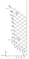
- FIG. 2 is a diagram for explaining a polishing marker of the first embodiment.
- FIG. 3 is a diagram for explaining the state of the integrated circuit chip shown in FIG. 2 after being polished.
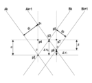
- FIG. 2 is a diagram for explaining the design of the polishing marker shown in FIG. 1 .
- 5A and 5B are diagrams illustrating a comparative example of the polishing method according to the first embodiment.
- 13A and 13B are diagrams for explaining polishing markers of an integrated circuit chip according to a second embodiment.
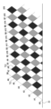
- 13A to 13C are diagrams for explaining polishing markers of an integrated circuit chip according to a third embodiment.
- FIG. 13 is a diagram for explaining a polishing marker according to the fourth embodiment.
- 13A, 13B, and 13C are diagrams for explaining advantages of the fourth embodiment.
- the first to fourth embodiments of the present disclosure will be described with reference to the drawings.
- the first to fourth embodiments will be collectively referred to as "the present embodiment.”
- the drawings used in the present embodiment are intended to explain the configuration, function, action, effect, and technical concept of the present disclosure, and are not intended to limit the specific configuration or shape of the present disclosure.
- Fig. 1 is a diagram for explaining a module including an integrated circuit chip with a polishing marker according to a first embodiment, in which the circuit includes an optical element.
- Fig. 1 is a schematic top view showing an integrated circuit chip (hereinafter, simply referred to as "chip") 1 having an optical waveguide polished using a polishing marker, and a fiber array 12.
- the fiber array 12 is connected to the chip 1.
- the chip 1 includes a plurality of optical waveguides 101 for input and output, and the fiber array 12 includes a plurality of optical fibers 103.
- the present disclosure aims to improve the polishing accuracy of the end face 30 of the chip 1 and to control the length A shown in Fig. 1 with high accuracy.
- FIG. 2 is a diagram for explaining the polishing markers of the first embodiment.
- the polishing markers are used to polish the end face 30 of the chip 1 having the optical waveguide 101.
- the polishing markers include a number of markers c1,0, c2,0, c3,0, c4,0... (hereinafter, when there is no need to distinguish between the individual markers, they will be referred to as marker c).
- marker c the distance between the end face 30 and each marker c is indicated by the length in the Y direction of the coordinates shown in the figure from the end face 30 to each marker c.
- the difference in distance from the end face 30 between adjacent markers is equal.
- the distances from the end face 30 of adjacent markers follow an arithmetic progression.
- the distance from the end face 30 to marker c0,0 is 0, the distance to marker c1,0 is 10 ⁇ m, the distance to marker c2,0 is 20 ⁇ m, the distance to marker c3,0 is 30 ⁇ m, and the distance to marker c4,0 is 40 ⁇ m.
- the notation of each marker c is based on the number of the intersecting line segment A and the number of the line segment B.
- the polishing marker of the first embodiment includes a first group of parallel lines that intersect the end face 30 of the chip 1 and include a plurality of first line segments that are parallel to each other, and a second group of parallel lines that intersect the end face 30 of the chip 1 and include a plurality of second line segments that are parallel to each other.
- the first line segments will be referred to as line segments A0 to A13
- the second line segments will be referred to as line segments B0 to B9.
- line segment A when the line segments A0 to A13 are not distinguished, they will simply be referred to as line segment A
- line segments B0 to B9 when the line segments B0 to B9 are not distinguished, they will simply be referred to as line segment B.
- Line segment A is within the plane of the chip 1 and intersects with a straight line 31 that is perpendicular to the end face 30 at an angle ⁇
- line segment B is within the plane of the chip 1 and intersects with a straight line 31 that is perpendicular to the end face 30 at an angle - ⁇ .
- the distance d1 between adjacent line segments A is different from the distance d2 between adjacent line segments B, and marker c is the intersection of line segments A and B. All intersections of line segments A and B can be marker c.
- the intersections of line segments A0 to A4 and B0 are shown marked with a ⁇ , but the intersections themselves become marker c, and marker c is not represented by a ⁇ .
- both line segment A and line segment B are formed using the layer used to create the waveguide. That is, in the first embodiment, a pattern of the line group of line segment A and the line group of line segment B are inserted into a mask used to etch the core layer, and the patterns of line segment A and line segment B are etched together with the core layer.
- the intersection of line segment A0 and line segment B0 is located on end face 30 before the chip is polished.
- chip end face 30 moves in the Y-axis direction according to the amount of polishing.
- the first embodiment can determine the amount of polishing by monitoring line segment A and line segment B, whose intersections coincide with the end face after the movement. This point will be explained in detail below.
- the first embodiment can determine the amount of polishing from 0 to 49 ⁇ m at 1 ⁇ m intervals in the range of lines A0 to A13 and lines B0 to B9 (k: 0 to 9, l: 0 to 4) shown in Figure 2.
- FIG. 3 is a diagram for explaining the state of the chip after polishing.
- the first embodiment can determine the polishing amount using the state of the intersection of line segment A5, line segment B4, and line segment A7, line segment B6 on the left and right of line segment A6 and line segment B5.
- the first embodiment since the interval d3 between line segment A5 and line segment B4 and the distance between line segment A7 and line segment B6 on the end surface 301 are approximately the same, it can be determined that the polishing amount is approximately the same as both 14 ⁇ m and 16 ⁇ m, in other words, that 15 ⁇ m has been polished accurately. In this way, it can be said that the first embodiment can use the information of the intersection lost by polishing to determine the polishing amount.
- FIG. 4 is a diagram for explaining the above formula.
- FIG. 4 is a diagram showing the state where line segments Ak and Ak+1 intersect with line segments Bk and Bk+1.
- the dashed lines shown in the diagram are auxiliary lines.
- Line segments Ak, Ak+1, Bk, and Bk+1 and the auxiliary lines form triangles p1, p4, p3 and p2, p4, p3, and triangles p5, p7, p3 and p6, p7, p3.
- Triangles p1, p4, p3 and triangles p2, p4, p3 are congruent to each other, and triangles p5, p7, p3 and triangles p6, p7, p3 are congruent to each other.
- FIGS. 5(a) and 5(b) are diagrams showing comparative examples of the polishing method of the first embodiment described above, showing a waveguide-type optical element 8 equipped with a polishing marker described in Patent Document 1.
- FIG. 5(a) is a top view showing a polishing marker 2 including markers 41 to 46 formed on an end face 40 of a waveguide-type optical element 8. When viewed from the top, markers 41 and 46, which have the same length, sandwich markers 42 to 45, which all have different lengths in the polishing direction.
- An optical waveguide 3 is formed parallel to the polishing marker 2.
- FIG. 5(b) is a diagram showing the polished surface of FIG. 5(a) according to the amount of polishing.
- marker 42 is the shortest, and the lengths increase successively toward marker 45. Therefore, as polishing progresses, marker 42 disappears first, and marker 45 remains last.
- the amount of polishing is determined based on which of markers 42 to 45 has disappeared due to polishing.
- the chip having the polishing markers of the first embodiment can improve the accuracy of determining the polishing amount by using not only the line segments A and B that have an intersection on the end surface 30, but also the line segments (line segments A5 and B4 in FIG. 3) whose intersection has already disappeared.
- the first embodiment can also use the line segments (line segments A7 and B6 in FIG. 3) whose intersection has not yet reached the end surface to determine the polishing amount. Therefore, the first embodiment can provide an integrated circuit chip polishing method and an integrated circuit chip that can be observed from above and can determine the polishing amount with high accuracy.
- the second embodiment differs from the first embodiment in that, while both line segment A and line segment B are formed by processing a core layer that forms a waveguide, one of line segment A and line segment B is formed in a layer different from the other line segment.
- Figures 6(a) and 6(b) are both diagrams for explaining the polishing markers of the integrated circuit chip of the second embodiment, and are top views showing an enlarged view of the intersection of line segments A and B.
- Figure 6(a) shows an example in which line segments An and Bn are formed by layers forming the same optical waveguide as in the first embodiment.
- Figure 6(b) shows an example in which line segment An is formed by a layer forming the optical waveguide of the second embodiment, and line segment Cn is formed by another layer.
- the layer forming the optical waveguide is made of quartz glass, silicon, or a compound semiconductor.
- line segment Cn is made of a metal material such as aluminum.
- the above configuration can be realized by adding the pattern of line segment An to a mask for patterning the core layer of the optical waveguide, and adding the pattern of line segment Cn to a mask for patterning the wiring layer.
- the third embodiment differs from the first embodiment in that it has a rectangular (parallelogram) shaped pattern layer formed by the intersection of line segments A and B of the first embodiment. That is, the second embodiment has a rectangular pattern layer whose outer edge is a group of parallel lines including a plurality of line segments A and a group of parallel lines including a plurality of line segments B intersecting with the group of parallel lines.
- FIG. 7 is a diagram for explaining a polishing marker for an integrated circuit chip according to a third embodiment.
- the polishing marker of the third embodiment includes a group of parallel lines including line segment A, and a group of parallel lines including line segment B.
- line segment A is indicated by a dashed line extending line segment A
- line segment B is indicated by a dashed line extending line segment B.
- line segment A and line segment B intersect, line segment A and line segment B form a parallelogram in top view.
- the third embodiment includes multiple pattern layers 601 that match this parallelogram.
- the multiple pattern layers 601 are arranged so that they only contact each other at the vertices c of the parallelogram, and do not contact the sides, in order to prevent the pattern layers 601 from being adjacent and indistinguishable. This arrangement is also called a checkered pattern. Each vertex of the pattern layer 601 functions as a marker c in the third embodiment.
- the pattern layer 601 is formed from a layer that forms a waveguide. Therefore, in the third embodiment, a pattern for forming the pattern layer 601 is added to the mask pattern that forms the core.
- the intersections of the line segments are used as the markers c, so the position of the markers c becomes ambiguous depending on the line width.
- each vertex c of a parallelogram (which coincides with the intersections of line segments A and B) is used as a marker, so ambiguity in the position can be avoided.
- the pattern layer 601 is made using a layer that forms a waveguide, but the pattern layer 601 may be made using any layer.
- the fourth embodiment further includes a rectangular pattern layer (second pattern layer) 702 formed in a layer different from the pattern layer 601, and having as its outer edges a group of parallel lines including a line segment A and a group of parallel lines including a line segment B intersecting the group of parallel lines, in addition to the multiple pattern layers 701.
- second pattern layer first pattern layer
- FIG. 8 is a diagram for explaining the polishing marker of the fourth embodiment. As shown in FIG. 8, pattern layer 701 and pattern layer 702 are arranged in a checkered pattern.
- the fourth embodiment has the advantage that, by forming pattern layers 701 and 702 on separate layers, the vertices of the parallelogram used as marker c are clearer than in the third embodiment.
- FIGS. 9(a), 9(b), and 9(c) are diagrams for explaining the above advantages.
- FIG. 9(a) and 9(b) are diagrams for explaining the disadvantages of forming pattern layers 81a, 81b, 81c, 81d, and 81e in a single layer.
- FIG. 9(a) is a diagram showing an example in which, when pattern layers 81a to 81e are formed in a single layer, the vertices of adjacent pattern layers 81a to 81e forming a check pattern are connected to each other, forming a connection portion 810. In such an example, the lines connecting the vertices have width and length, making the positions of the vertices unclear.
- FIG. 9(a) and 9(b) are diagrams for explaining the above advantages.
- FIG. 9(a) and 9(b) are diagrams for explaining the disadvantages of forming pattern layers 81a, 81b, 81c, 81d, and 81e in a single layer.
- FIG. 9(b) is a diagram showing an example in which the vertices of pattern layers 81a to 81e are separated from each other, resulting in gaps 71.
- the positions of the vertices of pattern layers 81a to 81e are unclear, similar to the example of FIG. 9(a). This phenomenon occurs due to the resolution of the exposure.
- FIG. 9(c) is a diagram for explaining the effect of the fourth embodiment, and is an example in which pattern layers 81a-81d and pattern layer 82 are provided on separate layers. Even in the fourth embodiment, it is unavoidable that the vertices of pattern layers 81a-81e will be slightly rounded. However, in the check pattern, the vertices meet adjacent pattern layers at a single point, making the marker clear.
- this embodiment shows an example in which the line segments A and B and the pattern layer are formed on a layer forming an optical waveguide or a wiring layer, but the line segments A and B and the pattern layer may be formed on any layer forming a circuit.
- this embodiment uses the intersection of two line segments or the vertex of a parallelogram as the marker, but the intersection is not limited to being formed by only two line segments, and may be any intersection that includes at least two intersecting line segments.
- the vertex is not limited to being the vertex of a parallelogram, and may be the vertex of any rectangle.
- this embodiment uses an integrated circuit chip including an optical element as an example, but the polishing marker of this disclosure does not utilize the properties of an optical circuit, so it can be applied to other integrated circuit chips such as electric circuit chips.
Landscapes
- Magnetic Heads (AREA)
Abstract
複数のマーカを含む研磨マーカを用い、集積回路チップの端面を研磨する研磨方法を提供する。研磨マーカ(2)は、集積回路チップの端面(30)と交差し、かつ互いに平行な線分(A)を複数含む平行線群と、端面(30)及び線分(A)と交差し、かつ互いに平行な線分(B)を含む平行線群と、を含み、隣り合う線分(A)同士の距離は、隣り合う線分(B)同士の距離と相違し、マーカ(c)は、線分(A)と線分(B)との交点である。これにより、研磨方法は、上面から観察し、高い精度で研磨量を判断できるようになる。
Description
本開示は、集積回路チップの研磨方法及び集積回路チップに係り、特に、研磨マーカを用いて研磨量をモニタする集積回路チップの研磨方法、及び研磨マーカを備えた集積回路チップに関する。
光通信装置の装置当たりの通信容量を増大させるため、導波路型光回路を用いた光部品の研究開発が進められている。導波路型光回路を用いることにより、光部品の更なる小型化、高機能化が期待される。光回路は、ウエハ上に作成されたのち、ウエハからダイシングされてチップに個片化される。チップの端面には光を入出力するための入出力導波路が設けられていて、光回路は入出力導波路を介して光ファイバに接続され、モジュール化される。
光ファイバと接続するチップ端面(接続端面)は、ブレードによるダイシングの場合、ブレード痕や小さなチッピング(欠け)等がある。ブレード痕やチッピングは、光を入出力する際に意図せぬ屈折や散乱を生むため、光損失の要因となり得る。この点を回避するため、接続端面は、ダイシングの後、光ファイバアレイを接続する前に研磨によって平滑化されることが多い。
研磨においては、チップを削り減らす長さを正確に制御して行うことが望ましい。チップのサイズを交差内に収めなければならない他、性能面に係るからである。すなわち、入出力導波路部分には微細な素子が配置されることがある。このような素子としては、例えば、スポットサイズコンバータ(SSC)がある。スポットサイズコンバータは、光のモードフィールド径(MFD)を光ファイバのMFDに近づけて接続損失を低減させる機能を有する。スポットサイズコンバータは、所望の性能を発揮するための適切な長さが決まっている。このため、チップ端面の研磨量が多すぎる、あるいは少なすぎると、光損失の増加等の性能劣化が起こり得る。
研磨量のモニタは、予めチップ端面にマーカを形成しておくことによって実施する。このようなマーカの例が、特許文献1に記載されている。特許文献1に開示されているマーカは、チップ端面からチップの内面に向けて延びる複数の線状のパターンを含んでいる。このようなマーカは、チップ端面を断面(研磨面)方向から観察した場合、チップ端面に残るパターンの数が研磨量が増すことに従って減少する。
しかしながら、研磨作業中にチップ端面を断面方向から観察することは、研磨の作業を中断しなければならず、作業効率の観点から好ましくない。また、特許文献1に記載のマーカは、上面から観察することも可能であるが、マーカの端がわずかに残っていてもそれを消えたと誤認する可能性があり、マーカに合せて研磨量を調整することは困難である。
本開示は、上記の点に鑑みてなされたものであり、上面から観察し、高い精度で研磨量を判断できる集積回路チップの研磨方法及び集積回路チップを提供することを目的とする。
上記目的を達成するために本開示の一形態の集積回路チップの研磨方法は、複数のマーカを含む研磨マーカを用い、集積回路チップの端面を研磨するための研磨方法であって、前記研磨マーカは、前記集積回路チップの端面と交差し、かつ互いに平行な第1の線分を複数含む第1の平行線群と、前記端面及び前記第1の線分と交差し、かつ互いに平行な第2の線分を含む第2の平行線群と、を含み、隣り合う前記第1の線分同士の距離は、隣り合う前記第2の線分同士の距離と相違し、前記マーカは、前記第1の線分と前記第2の線分との交点であり、前記交点を研磨量の基準とする。
本開示の一形態の集積回路チップは、複数のマーカを含む研磨マーカを備える集積回路チップであって、前記研磨マーカは、前記集積回路チップの端面と交差し、かつ互いに平行な第1の線分を複数含む第1の平行線群と、前記端面及び前記第1の線分と交差し、かつ互いに平行な第2の線分を含む第2の平行線群と、を含み、隣り合う前記第1の線分同士の距離は、隣り合う前記第2の線分同士の距離と相違し、前記マーカは、前記第1の線分と前記第2の線分との交点であり、前記交点が研磨量の基準となる。
以上の形態によれば、上面から観察し、高い精度で研磨量を判断できる集積回路チップの研磨方法及び集積回路チップを提供することができる。
本開示の第1の実施形態から第4の実施形態を、図面を用いて説明する。なお、第1の実施形態から第4の実施形態を相称して「本実施形態」とも記す。本実施形態に用いる図面は、本開示の構成、機能、作用、効果、技術思想を説明することを目的にし、本開示の具体的な構成や形状を限定するものではない。
(第1の実施形態)
図1は、第1の実施形態の研磨マーカ備えた集積回路チップを含むモジュールを説明するための図であって、回路は光学素子を含む。図1は、研磨マーカを使用して研磨される光導波路を有する集積回路チップ(以下、単に「チップ」と記す)1と、ファイバアレイ12と、を示す模式的な上面図である。図1において、ファイバアレイ12はチップ1と接続されている。チップ1は入出力用の光導波路101を複数備え、ファイバアレイ12は複数の光ファイバ103を備えている。本開示は、チップ1の端面30の研磨精度を高め、図1中に示す長さAを高い精度で制御することを目的とする。
図1は、第1の実施形態の研磨マーカ備えた集積回路チップを含むモジュールを説明するための図であって、回路は光学素子を含む。図1は、研磨マーカを使用して研磨される光導波路を有する集積回路チップ(以下、単に「チップ」と記す)1と、ファイバアレイ12と、を示す模式的な上面図である。図1において、ファイバアレイ12はチップ1と接続されている。チップ1は入出力用の光導波路101を複数備え、ファイバアレイ12は複数の光ファイバ103を備えている。本開示は、チップ1の端面30の研磨精度を高め、図1中に示す長さAを高い精度で制御することを目的とする。
図2は、第1の実施形態の研磨マーカを説明するための図である。研磨マーカは、光導波路101を備えるチップ1の端面30を研磨することに使用される研磨マーカである。研磨マーカは、複数のマーカc1,0、c2,0、c3,0、c4,0・・・を含む。(以下、マーカの各々を区別しない場合、マーカcと記す)。ここで、端面30と各マーカcとの距離を、端面30から各マーカcまでの図中に示す座標のY方向の長さで示す。
このような構成によれば、線分B0上に配置される複数のマーカcのうち、隣接するマーカ(例えばc1,0、c2,0)の端面30からの距離の差が等しくなる。換言すれば、隣接するマーカの端面30からの距離は、等差数列になっている。図2に示す例では、端面30からマーカc0,0の距離は0、マーカc1,0の距離は10μm、マーカc2,0の距離は20μm、マーカc3,0の距離は30μm、マーカc4,0の距離は40μmである。なお、各マーカcの表記は、交差する線分Aの番号と、線分Bの番号とに基づく。
第1の実施形態の研磨マーカは、チップ1の端面30と交差し、かつ互いに平行な第1の線分を複数含む第1の平行線群と、チップ1の端面30と交差し、かつ互いに平行な第2の線分を複数含む第2の平行線群と、を含む。以下、第1の線分を線分A0からA13とし、第2の線分を線分B0からB9とする。また、線分A0からA13を区別しない場合、単に線分Aとし、線分B0からB9を区別しない場合、単に線分Bとする。線分Aは、チップ1の面内にあって、かつ端面30と直交する直線31と角度θをもって交差し、線分Bは、チップ1の面内にあって、かつ端面30と直交する直線31と角度-θをもって交差する。
複数の線分のうち、隣り合う線分A同士の距離d1は、隣り合う線分B同士の距離d2と相違し、マーカcは、線分Aと線分Bとの交点である。全ての線分Aと全ての線分Bとの交点は、いずれもマーカcとなり得る。図2においては、説明のため、線分A0から線分A4と線分B0との交点に●を付して示しているが、交点自体がマーカcになり、マーカcは、●によって表されるものではない。
第1の実施形態は、線分A、線分Bを、いずれも導波路を作成する際のレイヤを使って形成する。すなわち、第1の実施形態は、コア層をエッチングする際のマスクに線分Aの線群と、線分Bの線群とのパターンを挿入し、コア層と共に線分A、線分Bのパターンをエッチングする。
第1の実施形態の構成によれば、チップの研磨前に線分A0と線分B0との交点が端面30上にある。研磨を開始すると、研磨量に応じてチップ端面30がY軸方向に移動する。この際、第1の実施形態は、移動後の端面と交点が一致する線分A、線分Bをモニタすることによって研磨量を判定することができる。以下、この点を具体的に説明する。
研磨前、線分A0と線分B0は、チップの端面30上で交差している。間隔d1と間隔d2とが異なるため、線分Aと線分Bの交点は、図2の左から右に向かうほどY方向に移動して端面30から離れる。端面30と交点cとの距離は、以下のように定量化することができる。
線分Ak+lと、線分Bkの交点と、端面30との距離は、
l×10+k (μm)
の式によって求められる。上記式によれば、
線分A1と線分B0との交点c1,0の端面30からの距離は、k=0、l=1となり、10μmと算出される。
線分A2と線分B0との交点c2,0の端面30からの距離は、k=0、l=2となり、20μmと算出される。
線分A3と線分B0との交点c3,0の端面30からの距離は、k=0、l=3となり、30μmと算出される。
線分A4と線分B0との交点c4,0の端面30からの距離は、k=0、l=4となり、40μmと算出される。
l×10+k (μm)
の式によって求められる。上記式によれば、
線分A1と線分B0との交点c1,0の端面30からの距離は、k=0、l=1となり、10μmと算出される。
線分A2と線分B0との交点c2,0の端面30からの距離は、k=0、l=2となり、20μmと算出される。
線分A3と線分B0との交点c3,0の端面30からの距離は、k=0、l=3となり、30μmと算出される。
線分A4と線分B0との交点c4,0の端面30からの距離は、k=0、l=4となり、40μmと算出される。
また、線分A1と線分B1との交点c1,1の端面30からの距離は、k=1、l=1となるので、11μmと算出される。
さらに、線分A13と線分B9との交点c13,9の端面30からの距離は、k=9、l=4となるので、49μmと算出される。
以上のように、第1の実施形態は、図2に示した線分A0から線分A13、線分B0から線分B9の範囲(k:0~9,l:0~4)で、1μm間隔で0から49μmまで研磨量を判定することが可能である。
図3は、研磨後のチップの状態を説明するための図である。図3に示す研磨マーカは、線分A6、線分B5の交点が研磨後の端面301に一致している。このため、図3に示すチップの研磨量は、k=5、l=1であるから、15μmと算出される。また、第1の実施形態は、このような算出の他、線分A6、線分B5の左右の線分A5、線分B4及び線分A7、線分B6の交点の状態を使って研磨量を判定することができる。すなわち、第1の実施形態は、端面301上において線分A5、線分B4の間隔d3、線分A7、線分B6の距離が同程度であることにより、研磨量は14μmと16μmとの両方と同程度に相違する、換言すれば、正確に15μm研磨されていると判定することができる。このように、第1の実施形態は、研磨によって失われた交点の情報をも研磨量の判定に使用し得ると言える。
図4は、上記した式を説明するための図である。図4は、線分Ak、線分Ak+1と、線分Bk、線分Bk+1とが交差した状態を示す図である。図中に示す破線は補助線である。線分Ak、線分Ak+1、線分Bk、線分Bk+1及び補助線は、三角形p1,p4,p3、三角形p2,p4,p3を形成し、三角形p5,p7,p3、三角形p6,p7,p3を形成する。三角形p1,p4,p3と三角形p2,p4,p3は互いに合同で、三角形p5,p7,p3と三角形p6,p7,p3は互いに合同である。
ここで、点p4,p2間の長さをαとすると、d1=2αsinθが成立する。ΔY2はαであるから、以下のように表される。
ΔY2=d1/(2・sinθ)
また、点p6,p7間の長さをβとすると、ΔY1=ΔY2-βと表される。β=d2/(2・sinθ)であるから、
ΔY1=(d1―d2)/(2・sinθ)となる。
ΔY2=d1/(2・sinθ)
また、点p6,p7間の長さをβとすると、ΔY1=ΔY2-βと表される。β=d2/(2・sinθ)であるから、
ΔY1=(d1―d2)/(2・sinθ)となる。
図5(a)、図5(b)は、以上説明した第1の実施形態の研磨方法の比較例を示す図であって、特許文献1に記載の研磨マーカを備えた導波路型光素子8を示している。図5(a)は、導波路型光素子8の端面40に形成されたマーカ41から46を含む研磨マーカ2を示す上面図である。上面視において、長さが等しいマーカ41、46は、マーカ42から45を挟み、マーカ42から45は、いずれも研磨方向の長さが異なっている。研磨マーカ2と平行に光導波路3が形成されている。図5(b)は、図5(a)の研磨面を研磨量に応じて示す図である。
図5(a)に示すように、マーカ42から45は、マーカ42が最も短く、マーカ45に向かって順次長くなっている。このため、研磨が進むうち、マーカ42が最も早く消失し、マーカ45が最後に残る。比較例では、このようなマーカ42から45のうちの研磨により消失したマーカを基準に研磨量を判定する。
しかしながら、このような比較例は、上面視においては研磨マーカ2のうちの完全に消失したものと、わずかに残っているものとの判定が難しい。残ったマーカを認識できない場合、研磨量が実際の量よりも多いと誤認する、すなわち研磨量を正確に判断できないことになる。また、研磨面の観察は、研磨を中断して行うため、作業効率の低下を招くおそれがある。このような比較例に対し、第1の実施形態の研磨マーカを有するチップは、端面30上に交点がある線分A、線分Bと共に、既に交点が消失している線分(図3における線分A5、線分B4)をも利用して研磨量の判定精度を高めることができる。さらに、第1の実施形態は、未だ交点が端面に達していない線分(図3における線分A7、線分B6)をも研磨量の判定に利用することができる。このため、第1の実施形態は、上面から観察し、高い精度で研磨量を判断できる集積回路チップの研磨方法、及び集積回路チップを提供することができる。
(第2の実施形態)
次に、本開示の第2の実施形態を説明する。第2の実施形態は、線分A、線分Bがいずれも導波路を形成するコア層を加工して形成するのに対し、線分A、線分Bの一方が、他方の線分と異なる層(レイヤ)で形成される点で第1の実施形態と相違する。
次に、本開示の第2の実施形態を説明する。第2の実施形態は、線分A、線分Bがいずれも導波路を形成するコア層を加工して形成するのに対し、線分A、線分Bの一方が、他方の線分と異なる層(レイヤ)で形成される点で第1の実施形態と相違する。
図6(a)、(b)は、いずれも第2の実施形態の集積回路チップの研磨マーカを説明するための図であって、線分A、線分Bの交差する部分を拡大して示す上面図である。図6(a)は、第1の実施形態と同様に同一の光導波路を形成する層により線分An、線分Bnを形成した例を示す。図6(b)は、第2の実施形態の光導波路を形成する層により線分Anを形成し、他の層により線分Cn形成した例を示す。光導波路を形成する層は、石英ガラス、シリコンや化合物半導体を材料とする。また、線分Cnは、線分Cnを例えば配線線層で形成する場合、アルミニウム等の金属材料で形成される。
上記の構成は、線分Anのパターンを光導波路のコア層をパターニングするマスクに追加し、線分Cnのパターンを、配線層をパターニングするマスクに追加することによって実現することができる。
線分An、線分Bnを単一のレイヤで形成する場合、フォトリソグラフィの露光分解能の限界から、図6(a)に示すように、交点の角が丸まってしまうことが避けられない。このような場合、交点が不明瞭になってしまうおそれがある。一方、線分An、線分Bnを別のレイヤで作製する場合、このような問題は発生しないため、交点がより明瞭に視認できるようになる。
(第3の実施形態)
次に、第3の実施形態を説明する。第3の実施形態は、第1の実施形態の線分A、線分Bが交差することにより形成される矩形(平行四辺形)形状のパターン層を有する点で第1の実施形態と相違する。すなわち、第2の実施形態は、線分Aを複数含む平行線群と、この平行線群と交差する線分Bを複数含む平行線群と、を外縁とする矩形形状のパターン層を有する。
次に、第3の実施形態を説明する。第3の実施形態は、第1の実施形態の線分A、線分Bが交差することにより形成される矩形(平行四辺形)形状のパターン層を有する点で第1の実施形態と相違する。すなわち、第2の実施形態は、線分Aを複数含む平行線群と、この平行線群と交差する線分Bを複数含む平行線群と、を外縁とする矩形形状のパターン層を有する。
図7は、第3の実施形態の集積回路チップの研磨マーカを説明するための図である。図7において、図2と同様の構成は同様の符号で示される。第3の実施形態の研磨マーカは、線分Aを含む平行線群と、線分Bを含む平行線群と、を含む。図7においては、線分Aを線分Aを延長した破線で示し、線分Bを線分Bを延長した破線で示す。線分Aと線分Bとが交差することにより、線分A、線分Bは上面視において平行四辺形を形成する。第3の実施形態は、この平行四辺形に一致するパターン層601を複数含む。
複数のパターン層601は、パターン層601が隣接して区別できなくなることを避けるため、平行四辺形の頂点cでのみ互いに接し、辺同士が接することがないように配置される。このような配置は、チェッカーパターンとも称される。パターン層601の各頂点は、第3の実施形態のマーカcとして機能する。
第3の実施形態は、パターン層601を導波路を形成する層で形成する。このため、第3の実施形態は、コアを形成するマスクのパターンにパターン層601を形成するためのパターンを追加する。
先に説明した第1の実施形態は、線分の交点をマーカcに利用しているため、線幅によりマーカcの位置が曖昧になる。第3の実施形態は、平行四辺形の各頂点c(線分A、線分Bの交点と一致)をマーカとして使用するため、その位置の曖昧さを回避することができる。なお、第3の実施形態は、導波路を形成する層を使ってパターン層601を作製したが、パターン層601はどのような層を使って作製してもよい。
(実施形態4)
第4の実施形態は、複数のパターン層701と共に、線分Aを含む平行線群、この平行線群と交差する線分Bを含む平行線群を外縁とし、パターン層601と異なる層に形成される矩形形状のパターン層(第2のパターン層)702をさらに有する。
第4の実施形態は、複数のパターン層701と共に、線分Aを含む平行線群、この平行線群と交差する線分Bを含む平行線群を外縁とし、パターン層601と異なる層に形成される矩形形状のパターン層(第2のパターン層)702をさらに有する。
図8は、第4の実施形態の研磨マーカを説明するための図である。図8に示すように、パターン層701と、パターン層702とはチェックパターン状に配置される。第4の実施形態は、パターン層701、702を別の層に形成することにより、マーカcとして使用される平行四辺形の頂点が第3の実施形態よりも明確になるという利点がある。
図9(a)、図9(b)及び図9(c)は、上記の利点について説明するための図である。図9(a)、図9(b)は、パターン層81a、81b、81c、81d、81eを単一の層に作製した場合の欠点を説明するための図である。図9(a)は、パターン層81a~81eを単一の層で作製した場合、チェックパターンを形成する隣り合うパターン層81a~81eの頂点同士がつながり、接続部分810を有する例を示す図である。このような例では、頂点同士をつなぐ線が幅と長さを持つため、頂点の位置が不明瞭になる。図9(b)は、パターン層81a~81eの頂点同士が離れ、隙間71が生じる例を示す図である。図9(b)の例は、図9(a)の例と同様に、パターン層81a~81eの頂点の位置が不明瞭になる。このような現象は、露光の解像度により生じる。
図9(c)は、第4の実施形態の効果を説明するための図であって、パターン層81a~81dと、パターン層82とを別の層に設けた例である。第4の実施形態においても、パターン層81a~81eの頂点がやや丸くなることは避けられない。しかし、チェックパターンにおいて隣接する他のパターン層と頂点が1点で接するため、マーカが明確になる。
なお、本開示は、以上説明した実施形態に限定されるものではない。例えば、本実施形態は、線分A、B、パターン層を光導波路を形成する層、あるいは配線層に形成する例を示したが、線分A、B、パターン層は回路を形成するどのような層に形成してもよい。また、本実施形態は、2本の線分の交点、または平行四辺形の頂点をマーカとしているが、交点は2本の線分のみによって形成されるものに限定されず、交差する2本の線分を少なくとも含むものであればよい。また、頂点は平行四辺形の頂点に限定されるものではなく、どのような矩形の頂点であってもよい。さらに、本実施形態は、光素子を含む集積回路チップを例にしたが、本開示の研磨マーカは光回路としての性質を利用したものではないから、電気回路チップ等の他の集積回路チップにも適用することが可能である。
集積回路チップ・・・1
光導波路・・・3
端面・・・30,301
71・・・隙間
81a~81e,601,701,702・・・パターン層
線分・・・A,B
マーカ・・・c
光導波路・・・3
端面・・・30,301
71・・・隙間
81a~81e,601,701,702・・・パターン層
線分・・・A,B
マーカ・・・c
Claims (5)
- 複数のマーカを含む研磨マーカを用い、集積回路チップの端面を研磨するための研磨方法であって、
前記研磨マーカは、
前記集積回路チップの端面と交差し、かつ互いに平行な第1の線分を複数含む第1の平行線群と、
前記端面及び前記第1の線分と交差し、かつ互いに平行な第2の線分を含む第2の平行線群と、を含み、
隣り合う前記第1の線分同士の距離は、隣り合う前記第2の線分同士の距離と相違し、
前記マーカは、前記第1の線分と前記第2の線分との交点であり、前記交点を研磨量の基準とする、
集積回路チップの研磨方法。 - 前記第1の線分及び前記第2の線分の一方は、他方の線分と異なる層に形成される、請求項1に記載の集積回路チップの研磨方法。
- 前記第1の平行線群と、当該第1の平行線群と交差する前記第2の平行線群と、を外縁とする矩形形状の第1のパターン層を有し、前記第1のパターン層は、チェックパターン状に配置される、請求項1に記載の集積回路チップの研磨方法。
- 前記第1の平行線群と、当該第1の平行線群と交差する前記第2の平行線群と、を外縁とし、前記第1のパターン層と異なる層に形成される矩形形状の第2のパターン層をさらに有し、前記第1のパターン層と前記第2のパターン層とはチェックパターン状に配置される、請求項3に記載の集積回路チップの研磨方法。
- 複数のマーカを含む研磨マーカを備える集積回路チップであって、
前記研磨マーカは、
前記集積回路チップの端面と交差し、かつ互いに平行な第1の線分を複数含む第1の平行線群と、
前記端面及び前記第1の線分と交差し、かつ互いに平行な第2の線分を含む第2の平行線群と、を含み、
隣り合う前記第1の線分同士の距離は、隣り合う前記第2の線分同士の距離と相違し、
前記マーカは、前記第1の線分と前記第2の線分との交点であり、前記交点が研磨量の基準となる、集積回路チップ。
Priority Applications (2)
| Application Number | Priority Date | Filing Date | Title |
|---|---|---|---|
| JP2025532337A JPWO2025013264A1 (ja) | 2023-07-12 | 2023-07-12 | |
| PCT/JP2023/025793 WO2025013264A1 (ja) | 2023-07-12 | 2023-07-12 | 集積回路チップの研磨方法及び集積回路チップ |
Applications Claiming Priority (1)
| Application Number | Priority Date | Filing Date | Title |
|---|---|---|---|
| PCT/JP2023/025793 WO2025013264A1 (ja) | 2023-07-12 | 2023-07-12 | 集積回路チップの研磨方法及び集積回路チップ |
Publications (1)
| Publication Number | Publication Date |
|---|---|
| WO2025013264A1 true WO2025013264A1 (ja) | 2025-01-16 |
Family
ID=94214857
Family Applications (1)
| Application Number | Title | Priority Date | Filing Date |
|---|---|---|---|
| PCT/JP2023/025793 Pending WO2025013264A1 (ja) | 2023-07-12 | 2023-07-12 | 集積回路チップの研磨方法及び集積回路チップ |
Country Status (2)
| Country | Link |
|---|---|
| JP (1) | JPWO2025013264A1 (ja) |
| WO (1) | WO2025013264A1 (ja) |
Citations (6)
| Publication number | Priority date | Publication date | Assignee | Title |
|---|---|---|---|---|
| JP2004085768A (ja) * | 2002-08-26 | 2004-03-18 | Fdk Corp | 光導波路デバイスとその製造方法 |
| JP2004233757A (ja) * | 2003-01-31 | 2004-08-19 | Fdk Corp | 光導波路素子の製造方法 |
| JP2009237326A (ja) * | 2008-03-27 | 2009-10-15 | Furukawa Electric Co Ltd:The | 光集積回路モジュール、このモジュールに用いる光学ベンチ、及び光集積回路モジュールの作製方法 |
| JP2011186171A (ja) * | 2010-03-08 | 2011-09-22 | Nippon Telegr & Teleph Corp <Ntt> | 導波路型光素子 |
| WO2017047076A1 (ja) * | 2015-09-18 | 2017-03-23 | 日本電気株式会社 | 光導波路素子 |
| WO2022130454A1 (ja) * | 2020-12-14 | 2022-06-23 | 日本電信電話株式会社 | 光導波路の光入出力部分の付近を保護するための金属層 |
-
2023
- 2023-07-12 WO PCT/JP2023/025793 patent/WO2025013264A1/ja active Pending
- 2023-07-12 JP JP2025532337A patent/JPWO2025013264A1/ja active Pending
Patent Citations (6)
| Publication number | Priority date | Publication date | Assignee | Title |
|---|---|---|---|---|
| JP2004085768A (ja) * | 2002-08-26 | 2004-03-18 | Fdk Corp | 光導波路デバイスとその製造方法 |
| JP2004233757A (ja) * | 2003-01-31 | 2004-08-19 | Fdk Corp | 光導波路素子の製造方法 |
| JP2009237326A (ja) * | 2008-03-27 | 2009-10-15 | Furukawa Electric Co Ltd:The | 光集積回路モジュール、このモジュールに用いる光学ベンチ、及び光集積回路モジュールの作製方法 |
| JP2011186171A (ja) * | 2010-03-08 | 2011-09-22 | Nippon Telegr & Teleph Corp <Ntt> | 導波路型光素子 |
| WO2017047076A1 (ja) * | 2015-09-18 | 2017-03-23 | 日本電気株式会社 | 光導波路素子 |
| WO2022130454A1 (ja) * | 2020-12-14 | 2022-06-23 | 日本電信電話株式会社 | 光導波路の光入出力部分の付近を保護するための金属層 |
Also Published As
| Publication number | Publication date |
|---|---|
| JPWO2025013264A1 (ja) | 2025-01-16 |
Similar Documents
| Publication | Publication Date | Title |
|---|---|---|
| US11011471B2 (en) | Semiconductor device | |
| CN107564907B (zh) | 两个波导之间的接合区域以及相关制造方法 | |
| US20070023932A1 (en) | Wafer, reticle, and exposure method using the wafer and reticle | |
| TWI502676B (zh) | 具預對準圖案的半導體晶圓和預對準半導體晶圓的方法 | |
| JP2002296760A (ja) | フォトマスク及びそれを用いた半導体装置の製造方法 | |
| WO2025013264A1 (ja) | 集積回路チップの研磨方法及び集積回路チップ | |
| JP3016776B1 (ja) | アライメントパタ―ンの形成方法及びマスクとの合わせ精度測定方法 | |
| US6632575B1 (en) | Precision fiducial | |
| CN114664794B (zh) | 晶圆键合标识及其形成方法、晶圆键合方法 | |
| US11977246B2 (en) | Mask orientation | |
| US6649529B2 (en) | Method of substrate processing and photoresist exposure | |
| US6456758B1 (en) | Chip for separating light into different wavelengths | |
| US20230092256A1 (en) | Mark, template, and semicondctor device manufacturing method | |
| KR20050120072A (ko) | 반도체 소자의 얼라인 마크 및 그를 이용한 얼라인 방법 | |
| EP4088094B1 (en) | Method to determine line angle and rotation of multiple patterning | |
| JP5009662B2 (ja) | フォトマスクの作製方法およびフォトマスク、ならびにそのフォトマスクを使用したデバイスの製造方法 | |
| KR100271631B1 (ko) | 반도체웨이퍼제조용얼라인키형성구조 | |
| WO2023064065A1 (en) | Alignment mark for front to back side alignment and lithography for optical device fabrication | |
| JP2007053138A (ja) | 半導体装置 | |
| KR20040058651A (ko) | 모니터링 포인트가 형성된 반도체 웨이퍼 | |
| JP2004233757A (ja) | 光導波路素子の製造方法 | |
| JP2007335459A (ja) | 半導体ウエハ、半導体装置、及び半導体装置の製造方法 | |
| JP2009139413A (ja) | 光学素子及びその製造方法 | |
| JPH03142820A (ja) | 半導体装置の製造方法 | |
| JPS62229923A (ja) | 半導体チツプにマ−クを形成する方法 |
Legal Events
| Date | Code | Title | Description |
|---|---|---|---|
| 121 | Ep: the epo has been informed by wipo that ep was designated in this application |
Ref document number: 23945137 Country of ref document: EP Kind code of ref document: A1 |
|
| ENP | Entry into the national phase |
Ref document number: 2025532337 Country of ref document: JP Kind code of ref document: A |
|
| WWE | Wipo information: entry into national phase |
Ref document number: 2025532337 Country of ref document: JP |
|
| NENP | Non-entry into the national phase |
Ref country code: DE |