WO2025013142A1 - 荷電粒子線装置 - Google Patents
荷電粒子線装置 Download PDFInfo
- Publication number
- WO2025013142A1 WO2025013142A1 PCT/JP2023/025337 JP2023025337W WO2025013142A1 WO 2025013142 A1 WO2025013142 A1 WO 2025013142A1 JP 2023025337 W JP2023025337 W JP 2023025337W WO 2025013142 A1 WO2025013142 A1 WO 2025013142A1
- Authority
- WO
- WIPO (PCT)
- Prior art keywords
- charged particle
- heater
- heat
- neg
- particle beam
- Prior art date
- Legal status (The legal status is an assumption and is not a legal conclusion. Google has not performed a legal analysis and makes no representation as to the accuracy of the status listed.)
- Ceased
Links
Images



Classifications
-
- H—ELECTRICITY
- H01—ELECTRIC ELEMENTS
- H01J—ELECTRIC DISCHARGE TUBES OR DISCHARGE LAMPS
- H01J37/00—Discharge tubes with provision for introducing objects or material to be exposed to the discharge, e.g. for the purpose of examination or processing thereof
- H01J37/02—Details
- H01J37/16—Vessels; Containers
-
- H—ELECTRICITY
- H01—ELECTRIC ELEMENTS
- H01J—ELECTRIC DISCHARGE TUBES OR DISCHARGE LAMPS
- H01J37/00—Discharge tubes with provision for introducing objects or material to be exposed to the discharge, e.g. for the purpose of examination or processing thereof
- H01J37/02—Details
- H01J37/04—Arrangements of electrodes and associated parts for generating or controlling the discharge, e.g. electron-optical arrangement or ion-optical arrangement
- H01J37/06—Electron sources; Electron guns
- H01J37/065—Construction of guns or parts thereof
-
- H—ELECTRICITY
- H01—ELECTRIC ELEMENTS
- H01J—ELECTRIC DISCHARGE TUBES OR DISCHARGE LAMPS
- H01J37/00—Discharge tubes with provision for introducing objects or material to be exposed to the discharge, e.g. for the purpose of examination or processing thereof
- H01J37/02—Details
- H01J37/18—Vacuum locks ; Means for obtaining or maintaining the desired pressure within the vessel
-
- H—ELECTRICITY
- H01—ELECTRIC ELEMENTS
- H01J—ELECTRIC DISCHARGE TUBES OR DISCHARGE LAMPS
- H01J37/00—Discharge tubes with provision for introducing objects or material to be exposed to the discharge, e.g. for the purpose of examination or processing thereof
- H01J37/26—Electron or ion microscopes; Electron or ion diffraction tubes
- H01J37/28—Electron or ion microscopes; Electron or ion diffraction tubes with scanning beams
-
- H—ELECTRICITY
- H01—ELECTRIC ELEMENTS
- H01J—ELECTRIC DISCHARGE TUBES OR DISCHARGE LAMPS
- H01J2237/00—Discharge tubes exposing object to beam, e.g. for analysis treatment, etching, imaging
- H01J2237/002—Cooling arrangements
Definitions
- the present invention relates to a charged particle beam device.
- a charged particle beam device is a device that generates an observation image of a sample by irradiating the sample with a charged particle beam such as an electron beam and detecting secondary electrons, transmitted electrons, reflected electrons, X-rays, etc. emitted from the sample.
- a high-brightness electron source charged particle source
- CFE cold field emission
- a CFE electron source emits an electron beam (charged particle beam) by concentrating an electric field at the tip of a sharpened single crystal (tip). If residual gas in the vacuum adheres to the tip of the tip, the amount of emitted current becomes unstable. For this reason, it is necessary to lower the pressure around the electron source (charged particle source) (increase the degree of vacuum).
- the electron source (charged particle source) is mounted in an electron gun (vacuum vessel) with the inside kept at a vacuum.
- a non-evaporable getter (NEG) material may be installed as a method of lowering the pressure inside the vacuum vessel. Unlike conventional evaporable getters, NEG material does not evaporate and retains its original shape even when heated (activated) in a vacuum. Once activated, the NEG material begins to adsorb and store gases, and has a vacuum exhaust effect when returned to room temperature.
- Patent Document 1 discloses an electron microscope equipped with NEG material near the extraction electrode.
- Patent Document 1 gives insufficient consideration to the activation temperature of the NEG material.
- the activation temperature of the NEG material is above a certain temperature, the vacuum exhaust effect does not occur and the pressure cannot be reduced.
- a stable electron beam charged particle beam
- the electron source charged particle source
- the present invention aims to provide a compact charged particle beam device that improves the activation temperature by efficiently heating the NEG material.
- the charged particle beam device comprises a vacuum vessel, a charged particle source including a single crystal needle, a filament connected to the single crystal needle, and an insulator that holds the filament, a non-evaporative getter material, an extraction electrode, a first vacuum chamber in which the charged particle source and the non-evaporative getter material are arranged and which is inside the extraction electrode, a heater for heating the non-evaporative getter material, a second vacuum chamber in which the heater and the extraction electrode are arranged and which has a higher pressure than the first vacuum chamber, and a heat absorption plate connected to the extraction electrode and arranged opposite the heater, the heater and the non-evaporative getter material being arranged in that order in the direction in which the charged particle beam is emitted from the charged particle source, and the non-evaporative getter material being arranged in the first vacuum chamber and the heater being arranged in the second vacuum chamber.
- the present invention provides a compact charged particle beam device that stabilizes the emission current by improving the activation temperature of the NEG material and efficiently reducing the pressure around the electron source (charged particle source).
- FIG. 1 is a schematic cross-sectional view showing an example of the overall configuration of a scanning electron microscope, which is an example of a charged particle beam device.
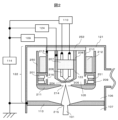
- 1 is a schematic cross-sectional view showing an example of a configuration of a CFE electron source and its periphery according to a first embodiment.
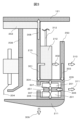
- 1 is a schematic cross-sectional view showing an example of the effect of the heat absorption plate of Example 1 in improving the heating efficiency of the NEG material.
- FIG. 1 is a schematic cross-sectional view showing an example of the effect of the emissivity of the extraction electrode of Example 1 in improving the heating efficiency of the NEG material.
- FIG. FIG. 13 is a diagram showing an example of the effect of the heat absorption plate of Example 1 in improving the heating efficiency of the NEG material.
- FIG. 11 is a diagram showing an example of the effect of the heat absorption plate of Example 1 in stabilizing the current of the electron beam.
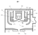
- FIG. A schematic cross-sectional view showing an example of a configuration in which the heat reflector of Example 2 improves the heating efficiency of the NEG material.
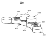
- FIG. 2 is a perspective view showing an example of an enlarged portion of the configuration of the NEG material of Example 1.
- a charged particle beam device is a device that irradiates a sample with a charged particle beam such as an electron beam, detects secondary electrons, transmitted electrons, reflected electrons, X-rays, etc. emitted from the sample, and generates an observation image of the sample.
- a charged particle beam such as an electron beam
- a scanning electron microscope is a device that irradiates an electron beam 101 onto a sample 102, detects secondary electrons and reflected electrons emitted from the sample 102, and generates an observation image of the sample 102. It is equipped with a mirror body 103 and a sample chamber 104, which keep the inside vacuum.
- the mirror body 103 is connected to a ground potential.
- the inside of the mirror body 103 is divided from the top into a first vacuum chamber 105, a second vacuum chamber 106, a third vacuum chamber 107, and a fourth vacuum chamber 108.
- An aperture through which the electron beam 101 passes is arranged in the center of the electrode separating the vacuum chambers, and differential pumping is performed.
- the pressure in each of the vacuum chambers 105, 106, 107, and 108 is higher in the lower vacuum chamber (vacuum chamber closer to the sample chamber 104). Below, each of the vacuum chambers 105, 106, 107, and 108 and the sample chamber 104 will be described.
- the first vacuum chamber 105 is a space inside the extraction electrode 203, and is evacuated by the NEG material 201.
- the pressure in the first vacuum chamber 105 is the lowest among the other vacuum chambers 106, 107, and 108, and is evacuated to an extremely high vacuum region of the order of 1 ⁇ 10 ⁇ 9 Pa to 1 ⁇ 10 ⁇ 10 Pa or less.
- a CFE electron source 202 is disposed in the first vacuum chamber 105, and an extraction electrode 203 is disposed to surround it.
- An acceleration power supply 114 is connected to the two pins of the CFE electron source 202 via a flashing power supply 110, and a negative acceleration voltage is normally applied relative to the ground potential supplied by the acceleration power supply 114.
- a suppressor power supply 124 is connected to the suppressor of the CFE electron source 202.
- the extraction electrode 203 has a cup shape and separates the first vacuum chamber 105 and the second vacuum chamber 106.
- An extraction power supply 109 is connected to the extraction electrode 203, and a positive extraction voltage is applied relative to the negative acceleration voltage applied to the two pins of the CFE electron source 202. When the extraction voltage is applied to the extraction electrode 203, an electron beam 101 is emitted from the CFE electron source 202.
- the flushing power supply 110 applies a voltage of several volts added to the negative acceleration voltage to one of the two pins, creating a potential difference of several volts between the two pins, and a pulse current is applied to the filament to heat it to about 2000°C (flushing).
- This flushing operation removes residual gas adsorbed to the CFE electron source 202 and resets the unstable time change in emission current.
- the first vacuum chamber 105 and the second vacuum chamber 106 are differentially evacuated, so there is a difference of several orders of magnitude in pressure between them. The details of the CFE electron source 202 and its surrounding configuration will be described later using Figure 2.
- the second vacuum chamber 106 is a space surrounded by the electron gun vacuum vessel 121 and the acceleration electrode 113 outside the extraction electrode 203, and is connected to the pipe 120.
- the pipe 120 has an ion pump 111 and an auxiliary NEG pump 112 at the end, and the second vacuum chamber 106 is evacuated to a vacuum.
- the pressure in the second vacuum chamber 106 is an ultra-high vacuum region of about 1 ⁇ 10 ⁇ 7 Pa to 1 ⁇ 10 ⁇ 9 Pa.
- the acceleration electrode 113 is disposed in the second vacuum chamber 106, and is isolated from the third vacuum chamber 107.
- the acceleration electrode 113 and the electron gun vacuum vessel 121 are connected to a ground potential.
- the electron beam 101 is accelerated to a predetermined speed according to the acceleration voltage.
- An electrostatic lens is formed in the space where the extraction electrode 203 and the acceleration electrode 113 face each other.
- the extraction electrode 203 and the acceleration electrode 113 have a Butler lens structure, which reduces the aberration of the electrostatic lens.
- the configuration above the acceleration electrode 113 is collectively referred to as an electron gun 122 .
- the third vacuum chamber 107 is evacuated by an ion pump 115.
- a condenser lens 116 is placed in the third vacuum chamber 107.
- the condenser lens 116 focuses the electron beam 101 and adjusts the amount of current, etc.
- a detector 117 is placed in the fourth vacuum chamber 108.
- the detector 117 detects secondary electrons and reflected electrons emitted from the sample 102.
- a plurality of detectors 117 may be provided, and may be placed in the sample chamber 104 or other vacuum chambers 105, 106, and 107.
- the sample chamber 104 is evacuated to a vacuum by a turbo molecular pump 118.
- An objective lens 119 and a sample 102 are placed in the sample chamber 104.
- the electron beam 101 is focused by the objective lens 119 and irradiated onto the sample 102.
- the CFE electron source 202 is composed of a tip 204, a filament 205, two pins 206, an insulator 207, and a suppressor 123.
- the tip 204 is a single crystal tungsten needle with a sharpened tip in the ⁇ 310> or ⁇ 111> orientation, and the radius of curvature of the tip is approximately 100 nm.
- the tip 204 is welded to the tip of the filament 205.
- the filament 205 is a polycrystalline tungsten wire shaped into a V-shaped hairpin. Pins 206 are welded to both ends of the filament 205.
- the two pins 206 are metal terminals, and are electrically insulated from each other by being held by the insulator 207.
- the suppressor 123 is attached to the outside of the insulator 207 by fitting, and contains the insulator 207, the pin 206, the filament 205, and a part of the tip 204.
- the suppressor 123 has an opening at the bottom, from which the tip of the tip 204 protrudes.
- the protruding length is about 0.1 mm to 1 mm.
- the holding part 208 is a metal cylinder, and holds the entire CFE electron source 202 by fixing the suppressor 123.
- the holding part 208 is connected to the electron gun vacuum vessel 121 via insulators 252, and is electrically insulated.
- the tip 204, filament 205, and pin 206 are at the same potential, and a negative acceleration voltage supplied from the acceleration power supply 114 is normally applied to them.
- a suppressor voltage is applied to the holding part 208 and suppressor 123 by the suppressor power supply 124.
- the flushing power supply 110 applies a voltage equal to the negative acceleration voltage plus a few volts to one of the two pins 206, and a potential difference of a few volts is created between the two pins 206, and the filament 205 is electrically heated, thereby removing (flushing) the residual gas adsorbed to the tip 204.
- the CFE electron source 202 does not need to have a suppressor 123, and can emit electron beams even without it.
- the extraction electrode 203 is composed of a metallic extraction electrode lower part 211, extraction electrode side wall 210, aperture 214, NEG unit 209, heat absorption plate 250, heat conduction plate 251, and NEG material 201.
- Stainless steel, titanium, permalloy, etc. are used as the main materials for the parts other than the NEG material 201.
- the extraction electrode lower part 211 is placed in a position closest to and facing the tip of the chip 204, and the two are separated by about 0.3 mm to 10 mm in the height direction.
- the extraction electrode lower part 211 is connected to the NEG unit 209.
- the NEG material 201 is placed inside the NEG unit 209.
- the NEG unit 209 is a thermally conductive container made of metal, and when heated, heat is transferred evenly throughout to maintain a constant temperature.
- the material of the NEG unit 209 may be stainless steel, titanium, permalloy, or other materials with high thermal conductivity such as copper, silver, gold, and aluminum. Alternatively, these may be formed as a film on the surface.
- the NEG unit 209 has an opening 216 only on the first vacuum chamber 105 side, and the first vacuum chamber 105 is evacuated using the NEG material 201.
- a thermally conductive plate 251 may be provided inside the NEG unit 209.
- the material of the thermally conductive plate 251 is the same as that of the NEG unit 209, and more preferably a material with high thermal conductivity is used, or these may be formed as a film.
- the NEG material 201 is a porous cylindrical pill made of a sintered alloy of zirconium, vanadium, and iron, and multiple pieces are arranged inside the NEG unit 209.
- the NEG material 201 may be other NEG materials and may have a shape other than a pill, such as a block, sheet, ring, thin film, or a combination of these. Also, only one piece may be arranged.
- the temperature at which the NEG material 201 is activated is approximately 500°C, and varies depending on the material. The closer the heating temperature of the NEG material 201 approaches this activation temperature, the faster the exhaust speed will be.
- An extraction voltage is applied to the extraction electrode 203, and its components are at the same potential.
- the extraction electrode sidewall 210 is connected to the electron gun vacuum vessel 121 via an insulator 252, and is electrically insulated.
- the electric field at the tip of the tip 204 is determined by the potential formed by the extraction electrode 203, and the electron beam 101 is emitted from the tip 204 by field emission.
- a positive or negative suppressor voltage is applied to the suppressor 123 with respect to the tip 204, and the electric field at the tip of the tip 204 is adjusted.
- An aperture 214 is disposed in the center of the lower part 211 of the extraction electrode.
- the hole diameter of the aperture 214 is typically 1 mm or less, and more preferably 0.5 mm or less.
- the electron beam 101 passes through a hole in the aperture 214 and travels to the second vacuum chamber 106, then expands into a cone shape before reaching the acceleration electrode 113.
- the aperture 215 is located in the center of the acceleration electrode 113. The outer periphery of the electron beam 101 is blocked by the aperture 215 and the acceleration electrode 113, and the central portion travels to the third vacuum chamber 107.
- the pressure in the vacuum chamber is lower as the effective pumping speed of the vacuum pump is higher and the amount of outgassing from the components in the vacuum chamber is smaller.
- the effective pumping speed is higher as the pumping speed of the vacuum pump itself is higher and the conductance of the exhaust path is larger.
- the effective pumping speed of the ion pump 111 and the auxiliary NEG pump 112 is limited by the conductance of the piping 120, and the effective pumping speed for exhausting the area around the electron source (charged particle source) is low.
- the NEG material 201 is arranged very close to the electron source (charged particle source) inside the extraction electrode 203, it has a large conductance and a high effective pumping speed.
- the area around the electron source (charged particle source) is efficiently evacuated to a vacuum.
- the first vacuum chamber 105 is a limited narrow space only inside the extraction electrode 203, and contains a small number of components, so the total amount of outgassing is small.
- the entire extraction electrode 203 is heated to a high temperature once by the heater 212, so the molten hydrogen inside the components is removed and the outgassing itself is reduced. As a result, the pressure in the first vacuum chamber 105 is efficiently reduced, and a stable emission current is obtained from the CFE electron source 202.
- a differential exhaust port 213 connecting the first vacuum chamber 105 and the second vacuum chamber 106 may be provided on the extraction electrode side wall 210.
- the conductance of the differential exhaust port 213 is reduced to create a pressure difference of several orders of magnitude between the first vacuum chamber 105 and the second vacuum chamber 106.
- the pressure in the first vacuum chamber 105 temporarily becomes higher than the pressure in the second vacuum chamber 106 due to the release of hydrogen gas and other gases from the NEG material 201. Gases such as hydrogen released from the NEG material 201 are released to the second vacuum chamber 106 through this differential exhaust port 213 and are pumped out by the ion pump 111 and the auxiliary NEG pump 112.
- the differential exhaust port 213 may be shaped like a circle or an elongated hole. It is also effective to make the opening area of the differential exhaust port 213 larger than the opening area of the aperture 214.
- the aperture 214 also acts as a differential exhaust hole, but because its hole diameter is small, its conductance is small and its effect is limited.
- the first vacuum chamber 105 and the second vacuum chamber 106 are isolated and differentially pumped, so that the pressure in the first vacuum chamber 105 is less likely to increase even if the pressure in the second vacuum chamber 106 increases.
- the pressure in the second vacuum chamber 106 may increase due to gas flowing in from the sample chamber 104, electron shock desorption gas emitted from the aperture 215 irradiated with the electron beam 101 or the acceleration electrode 113, sudden discharge, etc.
- the pressure increase in the first vacuum chamber 105 is several orders of magnitude smaller than the pressure increase in the second vacuum chamber 106. Therefore, even if the pressure in the second vacuum chamber 106 deteriorates, the pressure in the first vacuum chamber 105 remains low, and a stable emission current is maintained.
- Another advantage of differentially pumping the first vacuum chamber 105 and the second vacuum chamber 106 is that the electron gun 122 can be made smaller.
- the electron gun 122 can be made smaller, reducing costs and reducing the floor area or height of the charged particle beam device.
- the weight of the electron gun 122 is reduced, improving the resistance of the charged particle beam device to mechanical vibrations and improving resolution.
- the heater 212 is disposed in the second vacuum chamber 106 so as to contact the side of the extraction electrode side wall 210. By heating the heater 212 to 500°C or higher, the heat is transferred to the NEG unit 209 via the extraction electrode side wall 210, and the NEG material 201 inside is further heated and activated.
- the heater 212 is a ceramic heater such as alumina, silicon nitride, or boron nitride. Ceramic heaters are less susceptible to brittle fracture and disconnection than metal heaters, and are suitable for high-temperature heating.
- the heater 212 has a cylindrical structure and is in contact with the extraction electrode side wall 210 over a wide area to reduce thermal resistance, and efficiently transfers heat from the heater 212 to the extraction electrode side wall 210. Here, ceramic heaters may constantly release gas and worsen the pressure. Therefore, by disposing the heater 212 on the second vacuum chamber 106 side, the pressure in the first vacuum chamber 105 is prevented from worsening and the pressure in the first vacuum chamber 105 is minimized.
- the NEG unit 209 and the NEG material 201 inside it are positioned at different heights relative to the heater 212, with the heater 212 positioned above and the NEG unit 209 and NEG material 201 positioned below.
- the NEG unit 209 and NEG material 201 are positioned at positions spaced apart in the axial direction relative to the heater 212, with the NEG unit 209 and NEG material 201 positioned in front and the heater 212 positioned in the rearward direction.
- the heater 212, the NEG unit 209, and the NEG material 201 are arranged at different heights, and the horizontal positions of the two are overlapped to prevent the extraction electrode 203 from becoming large in the horizontal direction.
- the extraction electrode 203 can be made smaller even when the NEG unit 209 is provided.
- the electron gun vacuum vessel 121 and the electron gun 122 are made smaller, the resistance of the electron gun 122 to mechanical vibration is improved, and the resolution of the charged particle beam device is improved.
- the floor area for installing the charged particle beam device is reduced, and costs are reduced.
- the heater 212 can be made longer in the vertical direction, and the contact area of the heater 212 is increased, thereby improving the efficiency of heat transfer.
- the heat absorbing plate 250 faces the heater 212 and is positioned in a position directly facing the heater 212. There is no contact between the heat absorbing plate 250 and the heater 212.
- the heat absorbing plate 250 is connected to the NEG unit 209.
- the heat absorbing plate 250 absorbs the radiant heat emitted from the heater 212, becomes hot, and transfers this heat to the NEG unit 209, thereby improving the heating efficiency of the NEG material 201. This action is explained in Figure 3.
- the heat absorbing plate 250 in improving the heating efficiency of the NEG material 201 will be described with reference to FIG. 3.
- the heat generated by the heater 212 is transferred to the NEG unit 209 via the extraction electrode side wall 210.
- radiant heat 302 is emitted from the heater 212 heated to 500°C or higher.
- the amount of heat of the radiant heat 302 is proportional to the difference between the fourth power of the temperature of the heater 212 and the fourth power of the temperature of the heat absorbing plate 250 according to the Stefan-Boltzmann equation. As the temperature of the heat absorbing plate 250 increases, the radiant heat 302 decreases, and the temperature of the heater 212 increases with less power. Since the heat absorption plate 250 is connected to the NEG unit 209, heat is transferred from the heat absorption plate 250 to the NEG unit 209 as shown by the heat conduction path 303.
- the heat of the heater 212 is transferred to the NEG unit 209 through two paths, heat conduction path 301 and heat conduction path 303, and the NEG unit 209 is heated efficiently.
- the thermal resistance of the heat conduction from the heater 212 to the NEG unit 209 is reduced, and the temperature difference between the heater 212 and the NEG unit 209 is reduced.
- the reduced thermal resistance allows the heater 212 and the NEG unit 209 to be heated to a high temperature with less power.
- the heat absorption plate 250 may be assembled and connected as a separate part from the NEG unit 209, or may be manufactured as a single unit from the same material.
- Heat is transferred from the NEG unit 209 to the internal NEG material 201 via the paths shown by the thermal radiation path 304 and the thermal conduction path 305.
- the NEG material 201 is heated to a high temperature and activated, and the pumping capacity is realized.
- the NEG material 201 is entirely surrounded and contained within the NEG unit 209, and is not positioned protruding outside the NEG unit 209. Therefore, the entire NEG material 201 is heated evenly, and there are no locations where the temperature is uneven and activation is insufficient. As a result, the pumping speed is maximized. More preferably, all of the NEG material 201 is in thermal contact with the NEG unit 209, minimizing the temperature difference between the NEG material 201 and the NEG unit 209.
- a heat conductive plate 251 may be arranged inside the NEG unit 209. Using the heat conductive plate 251 improves the heating efficiency of the NEG material 201, and the temperature of the multiple NEG materials 201 becomes uniform. The heat conductive plate 251 is arranged in contact with the multiple NEG materials 201. Therefore, heat is transferred between the NEG materials 201, eliminating temperature bias, and maximizing the exhaust speed without any areas of insufficient activation. The heat conductive plate 251 may be in contact with the NEG unit 209. In this case, as shown by the heat conductive paths 306 and 307, heat is efficiently transferred from the NEG unit 209 to the NEG material 201, further reducing the temperature difference between the two.
- the order of temperature of each component when heated is from highest to lowest: heater 212, heat absorption plate 250, NEG unit 209, NEG material 201.
- heat is transferred from the higher temperature to the lower temperature by thermal conduction or thermal radiation.
- the temperature of the NEG material 201 becomes higher by placing it below the heater 212.
- heat conduction path 308 and the heat radiation paths 309, 310, and 311 heat escapes from the extraction electrode 203 to the outside when it is heated.
- the extraction electrode side wall 210 is connected to the electron gun vacuum vessel 121 via the insulator 252.
- the electron gun vacuum vessel 121 is exposed to the outside air at room temperature, so its temperature is low. Therefore, a large temperature difference occurs between the electron gun vacuum vessel 121 and the heater 212, and the amount of heat of the heat conduction path 308 is greater than that of the heat radiation paths 309, 310, and 311.
- the NEG material 201 is placed above the heater 212, that is, between the heater 212 and the electron gun vacuum vessel 121, a large amount of heat is absorbed by the electron gun vacuum vessel 121, so the temperature of the NEG material 201 drops rapidly compared to the heater 212, and it may not be possible to activate it.
- the NEG material 201 is placed below the heater 212, the only heat absorbed from this position is the radiant heat shown by the thermal radiation paths 309 and 311, and the amount of heat is less than that of the thermal conduction path 308. As a result, the NEG material 201 is maintained at a high temperature similar to that of the heater 212.
- the pressure around the tip 204 can be further reduced.
- the pressure around the tip 204 is reduced as the exhaust path between the tip 204 and the NEG material 201 is shortened to increase the conductance and increase the effective exhaust speed.
- the tip 204 is arranged opposite the lower extraction electrode 211, and is arranged below the entire extraction electrode 203. Therefore, by arranging the NEG material 201 below the extraction electrode 203, the distance of the exhaust path to the tip 204 is shortened. Therefore, the NEG unit 209 is connected to the lower extraction electrode 211, and the heater 212 is arranged above the NEG unit 209, and the effective exhaust speed can be improved.
- the heater 212 is placed below the NEG material 201 while leaving the position of the NEG material 201 unchanged, the distance between the chip 204 and the bottom side of the lower extraction electrode 211 will increase. In this case, the distance between the chip 204 and the electrostatic lens formed in the space where the lower extraction electrode 211 and the acceleration electrode 113 face each other will increase, increasing aberration and deteriorating resolution. For this reason, by placing the heater 212 above the NEG material 201 and shortening the distance between the chip 204 and the bottom side of the lower extraction electrode 211, the aberration of the electrostatic lens can be minimized.
- the heater 212 has wiring 312 for electrical heating.
- the wiring 312 is connected to a feedthrough (not shown) provided on the upper surface of the electron gun vacuum vessel 121, and power is supplied from an external power source. This wiring 312 must not come into contact with other electrodes and cause a short circuit.
- the length of the wiring 312 must be short.
- the heater 212 and NEG material 201 by placing the heater 212 on the top and the NEG material 201 on the bottom, in addition to miniaturizing the electron gun 122, the following effects are achieved: an increase in the heating temperature of the NEG material 201 and an increase in the effective exhaust speed, a reduction in the aberration of the electrostatic lens, and simplification of the wiring 312 of the heater 212.
- the above effects are achieved by placing the heater 212 first and then the NEG material 201 in the traveling direction in which the electron beam 101 is emitted.
- the heater 212 and NEG material 201 can be heated to high temperatures with little power. As shown by the heat radiation path 310, radiant heat escapes to the outside from the heat absorbing plate 250. If the heat absorbing plate 250 is brought into contact with the heater 212 and heated to the same high temperature, the radiant heat of the heat radiation path 310 will be greater and the power required for heating will be greater.
- the temperature of the heat absorbing plate 250 becomes slightly lower than that of the heater 212, and the radiant heat of the heat radiation path 310 decreases in proportion to the fourth power of that. As a result, less heat escapes to the outside, and it is possible to heat to a high temperature with less power.
- the heater 212 is a ceramic heater, and its dimensional accuracy is not good. For this reason, it is difficult to assemble the heater 212 by bringing both the inner and outer surfaces into contact with other electrodes. Keeping the heat absorbing plate 250 and heater 212 out of contact makes assembly easier.
- Another function of the heat absorbing plate 250 is to prevent the heater 212 from being charged.
- the heater 212 is made of ceramic, and becomes charged when the reflected electrons collide with it.
- the charged heater 212 forms an unintended potential distribution and bends the trajectory of the electron beam 101.
- off-axis aberration can cause a decrease in resolution, or the electron beam 101 can fail to reach the sample 102 due to a deviation in the trajectory.
- discharge occurs between the heater 212 and the surrounding electrodes. This can result in voltage fluctuations, causing problems such as melting of the tip 204 and destruction of the electrodes.
- the reflected electrons are prevented from colliding with the heater 212, and charging is prevented. Because the heat absorbing plate 250 is made of metal, it does not itself become charged. In addition, by further reflecting the reflected electrons from its surface, the reflected electrons are moved away from the heater 212, reducing the chance of collision. The upper end of the heat absorbing plate 250 is made higher than the upper end of the heater 212 to prevent the reflected electrons from reaching the heater 212. As a result, charging of the heater 212 is prevented, and deviations in the trajectory of the electron beam and discharge are prevented.
- Figure 8 is an oblique view of an enlarged portion of the NEG material 201.
- the NEG material 201 is preferably made of sintered porous bulk material, and multiple pieces are arranged inside the NEG unit 209.
- the surface area of the NEG material facing the vacuum increases compared to when a single NEG material with the same total volume is arranged. This increases the surface area that adsorbs gas, improving the pumping speed.
- sintered NEG material has a large effective surface area because it has micrometer-order irregularities on the surface. Therefore, it has a higher pumping speed and can reduce pressure more than NEG material with a smooth surface.
- the NEG materials 201 are cylindrically shaped and arranged closely together with their sides in contact with each other to increase the number of pieces mounted in the NEG unit 209.
- the points where the NEG materials 201 come into contact with each other are not exposed to the vacuum and do not contribute to vacuum evacuation, but by giving the NEG materials 201 a cylindrical structure and having the circles come into contact with each other, the contact area is minimized.
- the total area of the NEG materials 201 exposed to the vacuum increases, maximizing the evacuation speed.
- the NEG materials 201 may be stacked in two or more rows in the height direction, or may be arranged in two or more rows in the radial direction. The radial direction described in FIG.
- the structure of the NEG materials 201 may be a spherical structure or a three-dimensional structure with curved sides. In this case, the area where the NEG materials 201 come into contact with each other is also minimized.
- the NEG material 201 When a porous sintered body is used for the NEG material 201, its poor thermal conductivity can cause temperature differences between multiple NEG materials 201 or inside a single NEG material 201, resulting in some parts that cannot be activated. However, by using the heat conductive plate 251, the temperature difference is equalized, making it easier to activate the entire material.
- the NEG materials 201 may be placed above and below the heat conductive plate 251, as shown by the upper NEG material 802 and the lower NEG material 803.
- the width of the heat conductive plate 251 is made narrower than the diameter of the NEG material 201, and a part of the lower surface of the upper NEG material 802 and the upper surface of the lower NEG material 803 are exposed to the vacuum. As a result, the surface area contributing to exhaust is increased, improving the exhaust speed.
- the upper row NEG material 802 and the lower row NEG material 803 in contact with the same heat conductive plate 251, even if the NEG material 201 is arranged in multiple rows in the height direction, differences in temperature between the rows are prevented. As a result, the entire NEG material 201 is heated uniformly and activated.
- the circumferential NEG material 804 or NEG material 805 is also brought into contact with the heat conductive plate 251, so that at least three or more pieces are in contact. As a result, the temperature is uniform in two directions, the height direction and the circumferential direction.
- Multiple heat conduction plates 251 are arranged periodically in the circumferential direction, and more preferably, all of the NEG materials 201 are in contact with one of the heat conduction plates 251. As a result, the temperature of all of the NEG materials 201 in the NEG unit 209 is made uniform. Even when the NEG materials 201 are arranged in multiple rows in the radial direction, a heat conduction plate 251 is provided between the rows, and the NEG materials 201 in different rows are in contact with the same heat conduction plate 251, thereby preventing temperature bias due to the row.
- the thermally conductive plate 251 may have an opening 801.
- the opening 801 the surface of the NEG material 201 that is exposed to the vacuum and does not come into contact with the thermally conductive plate 251 increases. As a result, the exhaust speed improves.
- the thermally conductive plate 251 it is possible to both uniformize the heating temperature of the NEG material 201 and improve the exhaust speed by increasing the exposed area.
- NEG material 201 when NEG material is repeatedly exposed to the atmosphere and activated, adsorbed substances diffuse and accumulate inside, causing the pumping speed to decrease and the end of its life.
- bulk NEG material with a three-dimensional structure has sufficient volume, so there is a large capacity for adsorbed substances to diffuse inside. This gives it a long life despite repeated activation.
- sintered bulk material for NEG material 201 not only is the pumping speed improved, but the life is also extended.
- a metal with a low emissivity different from the base material of the electrode such as gold, silver, copper, aluminum, titanium nitride, etc., may be formed on the outer surface 401.
- the higher the emissivity of the inner surface 402 of the heat absorbing plate 250, the more it absorbs the radiant heat 302 emitted from the heater 212. As a result, the temperature of the heat absorbing plate 250 increases, and the temperature of the NEG material 201 also increases. Therefore, the surface roughness of the inner surface 402 is set to be greater than Ra 1 ⁇ m, and the emissivity is set to be 0.3 or more.
- a film of a material with a high emissivity different from the base material of the electrode, such as carbon or its compounds, or metal oxides, may be formed on the inner surface 402.
- the heat absorbing plate 250 has a lower emissivity on the outer surface than on the inner surface, thereby improving the heating efficiency of the NEG material 201.
- the NEG material 201 can be heated to a high temperature with less power.
- the NEG material 201 can be heated to a high temperature with less power.
- the NEG material 201 can be heated to a high temperature with less power.
- the pressure around the first vacuum chamber 105 and the electron source (charged particle source) is efficiently reduced by placing the NEG material 201 inside the extraction electrode 203, it is necessary to provide a space around the NEG material 201 to improve the conductance and increase the effective pumping speed.
- a space is provided around the NEG material 201, the path of thermal conduction to the NEG material 201 becomes narrower, and the heating temperature of the NEG material 201 becomes lower due to the difficulty in transferring heat, and the pumping speed may decrease without activation.
- the NEG material 201 in the configuration in which the NEG material 201 is placed inside the extraction electrode 203, there is a trade-off between improving the effective pumping speed of the NEG and improving the activation temperature.
- the NEG material 201 is a bulk material with a three-dimensional structure, a temperature distribution occurs within the three-dimensional structure of the NEG material 201, and some parts do not rise in temperature and are not activated, which may reduce the pumping capacity.
- the heating efficiency of the NEG material 201 is improved, and the heating temperature of the NEG material 201 becomes sufficiently high to activate it.
- the thermal resistance between the heater 212 and the NEG material 201 is reduced, the temperature difference between the two is reduced, and the heating efficiency is improved.
- the NEG material 201 can be heated to a high temperature even with less power to the heater 212.
- surrounding the NEG material 201 using the NEG unit 209 and the heat conduction plate 251 and transferring heat uniformly there is no temperature bias inside the NEG material 201, and the entire material is activated uniformly, maximizing the exhaust speed.
- the electron gun 122 is made smaller and the heating temperature and effective pumping speed of the NEG material 201 are improved.
- the electron gun 122 is made smaller and the heating temperature and effective pumping speed of the NEG material 201 are improved.
- the NEG material 201 is activated at a sufficiently high temperature, which efficiently reduces the pressure around the electron source (charged particle source), providing a stable electron beam, and providing a small electron gun and charged particle beam device.
- FIG. 5 shows the temperature of the NEG material 201 versus the input power of the heater 212.
- the power is normalized to 1 when the heat absorption plate 250 is present and the power at which the NEG material 201 reaches 500° C. is used.
- the NEG material 201 can be heated to 500°C by increasing the heater power.
- the temperature of the heater 212 and the extraction electrode 203 becomes excessively high, causing distortion of the electrodes and evaporation of the low-melting-point material.
- the extraction electrode 203 cannot be removed and reassembled due to electrode distortion, and the CFE electron source 202 and the NEG unit 209 cannot be replaced.
- the evaporation of the low-melting-point material causes the evaporated metal to be deposited on the insulators, etc., causing discharge, making it impossible to use the electron gun 122. For this reason, these problems can be prevented by heating the NEG material 201 to a high temperature with little power without heating the heater 212 and the extraction electrode 203 to an excessively high temperature, as in the present invention.
- FIG. 6 shows the stabilization time of the electron beam versus the pressure in the second vacuum chamber 106.
- the stabilization time is normalized to 1 when the pressure in the second vacuum chamber 106 is 1 ⁇ 10 ⁇ 9 Pa in the absence of the heat absorbing plate 250.
- the NEG is activated by diffusing the adsorbed material on the NEG surface to the inside to create a clean surface.
- the diffusion rate of the adsorbed material increases exponentially with the temperature, and the diffusion rate increases several times when the heating temperature increases by several percent. Therefore, a slight increase in the heating temperature of the NEG significantly changes the exhaust speed.
- the heat absorption plate 250 is provided to increase the heating temperature of the NEG material 201, and sufficient activation is performed to increase the pumping speed of the NEG material 201.
- the pressure in the second vacuum chamber 106 is reduced compared to when the heat absorption plate 250 is not provided, and the stabilization time of the electron beam emitted from the CFE electron source 202 is improved.
- the pressure in the second vacuum chamber 106 required to obtain the same stabilization time can be increased. This makes it possible to miniaturize or reduce the power required for the auxiliary NEG pump 112 and ion pump 111, thereby enabling the charged particle beam device to be miniaturized and reduced in cost.
- the heating efficiency of the NEG material 201 was improved and activated using a heat absorbing plate 250.
- a configuration including a heat reflecting plate 701 is described. Note that some of the configurations and functions described in the first embodiment can be applied to the second embodiment, so the same reference numerals are used for similar configurations and functions and the description is omitted.
- the heat reflector 701 is arranged in the second vacuum chamber 106 so as to surround the extraction electrode 203.
- the heat reflector 701 is made of stainless steel, titanium, permalloy, or the like, and is connected to the electron gun vacuum vessel 121 via the insulator 252.
- the heat reflector 701 has an opening 704 at the bottom center, and the electron beam 101 emitted from the CFE electron source 202 passes through this opening 704 and advances to the acceleration electrode 113 and aperture 215 below.
- the heat reflector 701 is electrically connected to the extraction power supply 109, and an extraction voltage is applied to it. Note that the voltage applied to the heat reflector 701 may be other voltages.
- the radiant heat is proportional to the difference between the fourth powers of the temperatures of the opposing objects, the radiant heat of the heat radiation paths 310 and 311 becomes relatively large, and a large amount of heat is taken away from the extraction electrode 203.
- the heat reflector 701 in a position surrounding the extraction electrode 203 as in this embodiment, the extraction electrode 203 and the heat reflector 701 face each other.
- the temperature of the heat reflector 701 becomes intermediate between the temperatures of the extraction electrode 203 and the electron gun vacuum vessel 121, and the radiant heat shown by the heat radiation paths 310 and 311 is reduced. As a result, the amount of heat escaping from the extraction electrode 203 is reduced, and the NEG material 201 can be heated to a high temperature even with a reduced input power to the heater 212.
- a metal with a low radiation coefficient different from the base material of the heat reflector such as gold, silver, copper, aluminum, or titanium nitride, may be formed.
- the radiant heat transmitted from the heat reflector 701 to the electron gun vacuum vessel 121 shown by the heat radiation path 703 is reduced.
- the temperature of the heat reflector 701 increases, and the radiant heat shown by the heat radiation paths 310 and 311 is further reduced.
- the NEG material 201 can be heated to a high temperature even with even less input power to the heater 212.
- the acceleration electrode 113 may be provided with a second heater 702.
- the second heater 702 is a ceramic heater and is placed in contact with the acceleration electrode 113.
- the second heater 702 is also placed in the third vacuum chamber 107, so that even if there is steady degassing, the pressure in the second vacuum chamber 106 will not deteriorate.
- the second heater 702 is heated at the same time as the heater 212 is heated, and the acceleration electrode 113 and the aperture 215 are heated to about 500°C.
- the temperature difference between the extraction electrode 203 and the acceleration electrode 113 is reduced, and the radiated heat of the thermal radiation path 309 is reduced. Therefore, the amount of heat escaping from the extraction electrode 203 is reduced, and the NEG material 201 can be heated to a high temperature even if the input power of the heater 212 is further reduced.
- the acceleration electrode 113 and the aperture 215 the amount of electron-stimulated desorption gas released when the electron beam 101 collides with them is reduced. As a result, the pressure in the second vacuum chamber 106 is prevented from deteriorating.
- tungsten single crystal instead of tungsten single crystal, a low work function material such as CeB6 or LaB6, or a material with an inactive surface such as a carbon-coated material may be used as the tip 204.
- a nanowire electron source with a sharpened tip radius of curvature of several tens of nm or several atoms to one atom, or a single-atom electron source may be used.
- the charged particle source to which the present invention can be applied is not limited to a CFE electron source, but can also be applied to a Schottky electron source or an ion source.
- a gas field ionization ion source can be cited as an ion source, and by using a tungsten single crystal with a ⁇ 111> crystal orientation for the tip 204 and applying a positive voltage to the tip 204 with respect to the extraction electrode 203, ions can be emitted as a charged particle beam from the tip 204 even if the other device configurations are almost the same.
- an ultra-high vacuum of 1 ⁇ 10 ⁇ 7 Pa or less is required.
Landscapes
- Chemical & Material Sciences (AREA)
- Analytical Chemistry (AREA)
- Electron Sources, Ion Sources (AREA)
Abstract
Description
Claims (14)
- 単結晶針と該単結晶針と接続したフィラメントと該フィラメントを保持する碍子とを備えた荷電粒子源と、
非蒸発ゲッター材と、
引出電極と、
前記荷電粒子源と前記非蒸発ゲッター材とを配置し、前記引出電極の内部にある第一の真空室と、
前記非蒸発ゲッター材を加熱するヒーターと、
前記ヒーターと前記引出電極とを配置し、前記第一の真空室より圧力が高い第二の真空室と、
前記引出電極に接続し、前記ヒーターと対向させて配置した熱吸収板と、を備える荷電粒子線装置であって、
前記荷電粒子源から荷電粒子線が放出される方向に対して前記ヒーター、前記非蒸発ゲッター材が順番に配置され、且つ、前記非蒸発ゲッター材は前記第一の真空室に配置され、前記ヒーターは第二の真空室に配置されることを特徴とする荷電粒子線装置。 - 前記引出電極は前記第一の真空室側に開口を備えた熱伝導容器を備え、
該熱伝導容器はその内部に複数の前記非蒸発ゲッター材を備えることを特徴とする請求項1に記載の荷電粒子線装置。 - 前記熱吸収板が前記熱伝導容器に接続されることを特徴とする請求項2に記載の荷電粒子線装置。
- 前記ヒーターの加熱時において前記熱吸収板の温度は前記非蒸発ゲッター材の温度よりも高いことを特徴とする請求項3に記載の荷電粒子線装置。
- 前記非蒸発ゲッター材は立体構造をもつ焼結体であることを特徴とする請求項3に記載の荷電粒子線装置。
- 前記非蒸発ゲッター材は曲線形状の側面もち、
複数の前記非蒸発ゲッター材が前記側面で接触されることを特徴とする請求項5に記載の荷電粒子線装置。 - 前記熱伝導容器は内部に熱伝導板を備え、
該熱伝導板は少なくとも3つ以上の前記非蒸発ゲッター材と接触されることを特徴とする請求項2に記載の荷電粒子線装置。 - 前記熱伝導板は開口を備えることを特徴とする請求項7に記載の荷電粒子線装置。
- 前記ヒーターはセラミック製であり、
前記熱吸収板は前記荷電粒子線が生成する反射粒子が前記ヒーターに衝突することを防ぐ部材であることを特徴とする請求項1に記載の荷電粒子線装置。 - 前記熱吸収板の前記ヒーターと向き合う内側の面の輻射率は外側の輻射率よりも高いことを特徴とする請求項1に記載の荷電粒子線装置。
- 前記熱吸収板の内側の面の表面粗さは外側の表面粗さよりも大きいことを特徴とする請求項10に記載の荷電粒子線装置。
- 前記熱吸収板の内側と外側の表面の材料が異なることを特徴とする請求項11に記載の荷電粒子線装置。
- 前記第二の真空室に熱反射板を備え、
該熱反射板は前記引出電極を囲むように配置されることを特徴とする請求項1に記載の荷電粒子線装置。 - 前記引出電極と向き合う位置に加速電極を備え、
前記加速電極は第二のヒーターを備えることを特徴とする請求項1に記載の荷電粒子線装置。
Priority Applications (4)
| Application Number | Priority Date | Filing Date | Title |
|---|---|---|---|
| KR1020257029527A KR20250142415A (ko) | 2023-07-07 | 2023-07-07 | 하전 입자선 장치 |
| PCT/JP2023/025337 WO2025013142A1 (ja) | 2023-07-07 | 2023-07-07 | 荷電粒子線装置 |
| JP2025532238A JPWO2025013142A1 (ja) | 2023-07-07 | 2023-07-07 | |
| TW113121251A TWI881856B (zh) | 2023-07-07 | 2024-06-07 | 帶電粒子線裝置 |
Applications Claiming Priority (1)
| Application Number | Priority Date | Filing Date | Title |
|---|---|---|---|
| PCT/JP2023/025337 WO2025013142A1 (ja) | 2023-07-07 | 2023-07-07 | 荷電粒子線装置 |
Publications (1)
| Publication Number | Publication Date |
|---|---|
| WO2025013142A1 true WO2025013142A1 (ja) | 2025-01-16 |
Family
ID=94215230
Family Applications (1)
| Application Number | Title | Priority Date | Filing Date |
|---|---|---|---|
| PCT/JP2023/025337 Ceased WO2025013142A1 (ja) | 2023-07-07 | 2023-07-07 | 荷電粒子線装置 |
Country Status (4)
| Country | Link |
|---|---|
| JP (1) | JPWO2025013142A1 (ja) |
| KR (1) | KR20250142415A (ja) |
| TW (1) | TWI881856B (ja) |
| WO (1) | WO2025013142A1 (ja) |
Citations (4)
| Publication number | Priority date | Publication date | Assignee | Title |
|---|---|---|---|---|
| JPS63202832A (ja) * | 1987-02-17 | 1988-08-22 | Fujitsu Ltd | 電子銃 |
| JP2006294481A (ja) * | 2005-04-13 | 2006-10-26 | Hitachi High-Technologies Corp | 荷電粒子線装置 |
| JP2007157682A (ja) * | 2005-11-10 | 2007-06-21 | Hitachi High-Technologies Corp | 荷電粒子線装置 |
| JP2010010125A (ja) * | 2008-05-28 | 2010-01-14 | Hitachi High-Technologies Corp | 荷電粒子線装置 |
Family Cites Families (1)
| Publication number | Priority date | Publication date | Assignee | Title |
|---|---|---|---|---|
| DE112016007160B4 (de) | 2016-09-23 | 2022-07-28 | Hitachi High-Tech Corporation | Elektronenmikroskop |
-
2023
- 2023-07-07 WO PCT/JP2023/025337 patent/WO2025013142A1/ja not_active Ceased
- 2023-07-07 KR KR1020257029527A patent/KR20250142415A/ko active Pending
- 2023-07-07 JP JP2025532238A patent/JPWO2025013142A1/ja active Pending
-
2024
- 2024-06-07 TW TW113121251A patent/TWI881856B/zh active
Patent Citations (4)
| Publication number | Priority date | Publication date | Assignee | Title |
|---|---|---|---|---|
| JPS63202832A (ja) * | 1987-02-17 | 1988-08-22 | Fujitsu Ltd | 電子銃 |
| JP2006294481A (ja) * | 2005-04-13 | 2006-10-26 | Hitachi High-Technologies Corp | 荷電粒子線装置 |
| JP2007157682A (ja) * | 2005-11-10 | 2007-06-21 | Hitachi High-Technologies Corp | 荷電粒子線装置 |
| JP2010010125A (ja) * | 2008-05-28 | 2010-01-14 | Hitachi High-Technologies Corp | 荷電粒子線装置 |
Also Published As
| Publication number | Publication date |
|---|---|
| TW202503804A (zh) | 2025-01-16 |
| TWI881856B (zh) | 2025-04-21 |
| JPWO2025013142A1 (ja) | 2025-01-16 |
| KR20250142415A (ko) | 2025-09-30 |
Similar Documents
| Publication | Publication Date | Title |
|---|---|---|
| US10903037B2 (en) | Charged particle beam device | |
| US8472586B2 (en) | X-ray source and X-ray photographing apparatus including the source | |
| CN110870036B (zh) | 紧凑型电离射线生成源、包括多个源的组件以及用于生产该源的方法 | |
| US20080283745A1 (en) | Emitter chamber, charged partical apparatus and method for operating same | |
| US10636623B2 (en) | Ion beam device | |
| WO2012063379A1 (ja) | 電界放射装置及び携帯型非破壊検査装置 | |
| JP6095338B2 (ja) | 電子銃および荷電粒子線装置 | |
| KR101586342B1 (ko) | 제전 범위 및 방열 기능이 향상된 연엑스선 발생 장치 | |
| WO2018055715A1 (ja) | 電子顕微鏡 | |
| EP3142138A1 (en) | X-ray tube | |
| WO2025013142A1 (ja) | 荷電粒子線装置 | |
| US7657003B2 (en) | X-ray tube with enhanced small spot cathode and methods for manufacture thereof | |
| TWI900839B (zh) | 帶電粒子線裝置 | |
| TWI913861B (zh) | 帶電粒子線裝置與電子槍 | |
| CN110870035B (zh) | 用于生成电离射线的紧凑型源 | |
| JP7502359B2 (ja) | 荷電粒子線源および荷電粒子線装置 | |
| JP4781156B2 (ja) | 透過型x線管 | |
| TW202514694A (zh) | 帶電粒子線裝置與電子槍 | |
| JP5661368B2 (ja) | X線発生装置 | |
| US12580147B2 (en) | X-ray tube | |
| RU2797346C1 (ru) | Катод рентгеновской трубки | |
| JP5159724B2 (ja) | 電子銃、電子銃を用いた真空処理装置 | |
| TWI544101B (zh) | 用於具火花擴散空間限制之電弧汽化的標靶 | |
| JP2011040293A (ja) | 電子銃、電子銃を用いた真空処理装置 | |
| JP2011040292A (ja) | 電子銃、電子銃を用いた真空処理装置 |
Legal Events
| Date | Code | Title | Description |
|---|---|---|---|
| 121 | Ep: the epo has been informed by wipo that ep was designated in this application |
Ref document number: 23945023 Country of ref document: EP Kind code of ref document: A1 |
|
| ENP | Entry into the national phase |
Ref document number: 2025532238 Country of ref document: JP Kind code of ref document: A |
|
| WWE | Wipo information: entry into national phase |
Ref document number: 2025532238 Country of ref document: JP |
|
| ENP | Entry into the national phase |
Ref document number: 1020257029527 Country of ref document: KR Free format text: ST27 STATUS EVENT CODE: A-0-1-A10-A15-NAP-PA0105 (AS PROVIDED BY THE NATIONAL OFFICE) |
|
| NENP | Non-entry into the national phase |
Ref country code: DE |