WO2025009417A1 - 電源装置及び車両 - Google Patents
電源装置及び車両 Download PDFInfo
- Publication number
- WO2025009417A1 WO2025009417A1 PCT/JP2024/022596 JP2024022596W WO2025009417A1 WO 2025009417 A1 WO2025009417 A1 WO 2025009417A1 JP 2024022596 W JP2024022596 W JP 2024022596W WO 2025009417 A1 WO2025009417 A1 WO 2025009417A1
- Authority
- WO
- WIPO (PCT)
- Prior art keywords
- storage element
- converter
- current
- power supply
- conversion
- Prior art date
- Legal status (The legal status is an assumption and is not a legal conclusion. Google has not performed a legal analysis and makes no representation as to the accuracy of the status listed.)
- Ceased
Links
Images






Classifications
-
- B—PERFORMING OPERATIONS; TRANSPORTING
- B62—LAND VEHICLES FOR TRAVELLING OTHERWISE THAN ON RAILS
- B62D—MOTOR VEHICLES; TRAILERS
- B62D5/00—Power-assisted or power-driven steering
- B62D5/04—Power-assisted or power-driven steering electrical, e.g. using an electric servo-motor connected to, or forming part of, the steering gear
-
- H—ELECTRICITY
- H02—GENERATION; CONVERSION OR DISTRIBUTION OF ELECTRIC POWER
- H02J—ELECTRIC POWER NETWORKS; CIRCUIT ARRANGEMENTS OR SYSTEMS FOR SUPPLYING OR DISTRIBUTING ELECTRIC POWER; SYSTEMS FOR STORING ELECTRIC ENERGY
- H02J1/00—Circuit arrangements for DC mains or DC distribution networks
-
- H—ELECTRICITY
- H02—GENERATION; CONVERSION OR DISTRIBUTION OF ELECTRIC POWER
- H02J—ELECTRIC POWER NETWORKS; CIRCUIT ARRANGEMENTS OR SYSTEMS FOR SUPPLYING OR DISTRIBUTING ELECTRIC POWER; SYSTEMS FOR STORING ELECTRIC ENERGY
- H02J7/00—Circuit arrangements for charging or discharging batteries or for supplying loads from batteries
-
- H—ELECTRICITY
- H02—GENERATION; CONVERSION OR DISTRIBUTION OF ELECTRIC POWER
- H02M—APPARATUS FOR CONVERSION BETWEEN AC AND AC, BETWEEN AC AND DC, OR BETWEEN DC AND DC, AND FOR USE WITH MAINS OR SIMILAR POWER SUPPLY SYSTEMS; CONVERSION OF DC OR AC INPUT POWER INTO SURGE OUTPUT POWER; CONTROL OR REGULATION THEREOF
- H02M3/00—Conversion of DC power input into DC power output
Definitions
- This disclosure relates to a power supply device and a vehicle equipped with the power supply device.
- the power supply device of Patent Document 1 has a first storage element, a second storage element connected in parallel to the first storage element and having a smaller internal resistance and storage capacity than the first storage element, an opening/closing unit connected between the first storage element and the second storage element and switching between a disconnected state and a connected state, a charging circuit connected to the input path of the first storage element and performing a step-down operation, a discharging circuit connected to the output path of the second storage element and performing a step-up operation, and a control circuit that controls the operation of the opening/closing unit, the charging circuit, and the discharging circuit.
- the first storage element and the second storage element are connected via an opening/closing part, so in order to ensure that the second storage element can be charged from the first storage element via the opening/closing part, it is necessary that the voltage of the first storage element is higher than the voltage of the second storage element.
- a power supply device has an output terminal connected to a load and supplies power to the load via the output terminal, and includes a first storage element, a first DC/DC converter inserted in a path between the first storage element and the output terminal, and performing at least the first conversion of converting a voltage input from the first storage element and outputting it to the output terminal, and a second conversion of converting a voltage input from the output terminal and outputting it to the first storage element, a second storage element, a second DC/DC converter inserted in a path between the second storage element and the output terminal, and performing a third conversion of converting a voltage input from the second storage element and outputting it to the output terminal, and a fourth conversion of converting a voltage input from the output terminal and outputting it to the second storage element, and a control circuit for controlling the first DC/DC converter and the second DC/DC converter, and the control circuit has a large current mode in which the first DC/DC converter performs the first conversion and the second DC/DC converter performs the third conversion
- the present disclosure provides a power supply device equipped with two storage elements that does not require a switch to connect the two storage elements and is not restricted by the component types of the two storage elements, and a vehicle equipped with such a power supply device.
- FIG. 1 is a block diagram showing a configuration of a backup power supply device according to an embodiment.
- FIG. 2 is a circuit diagram showing a specific example of the first DC/DC converter and the second DC/DC converter in FIG.
- FIG. 3A is a diagram showing a current flow in a normal current mode of a backup power supply device according to an embodiment.
- FIG. 3B is a diagram showing a current flow in the high current mode of the backup power supply device according to the embodiment.
- FIG. 4 is a diagram showing an example of operation of the backup power supply device according to the embodiment in the normal current mode.
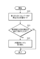
- FIG. 5A is a flowchart showing the operation of the backup power supply device according to the embodiment when it switches from the normal current mode to the large current mode.
- FIG. 5A is a flowchart showing the operation of the backup power supply device according to the embodiment when it switches from the normal current mode to the large current mode.
- FIG. 5B is a diagram showing the state change of the backup power supply device when switching from the normal current mode shown in FIG. 5A to the large current mode.
- FIG. 6A is a flowchart showing a procedure for switching the backup power supply device according to the embodiment from the normal current mode to the high current mode in a manner different from that shown in FIG. 5A.
- FIG. 6B is a diagram for supplementarily explaining the switching from the normal current mode to the large current mode shown in FIG. 6A.
- FIG. 7 is a diagram for explaining a control procedure for avoiding successive switching between the charging mode and the stop mode.
- FIG. 8 is a block diagram showing the configuration of a backup power supply device according to a first modified example of the embodiment.
- the first storage element 11 is a storage element capable of storing and supplying electric charge, and in this embodiment, is a storage element having a larger storage capacity and a smaller output current (i.e., a larger internal resistance) than the second storage element 13.
- the first storage element 11 is a single lithium-ion battery (hereinafter also referred to as "LiB").
- LiBs have a voltage of 1.8V to 4.2V depending on the charge state.
- the first DC/DC converter 12 is an example of a DC/DC converter that is inserted in a path between the first storage element 11 and the output terminal 20, and performs at least the first conversion (i.e., discharging from the first storage element 11) of converting a voltage input from the first storage element 11 side and outputting it to the output terminal 20 side, and the second conversion (i.e., charging to the first storage element 11) of converting a voltage input from the output terminal 20 side and outputting it to the first storage element 11 side.
- the first DC/DC converter 12 is a unidirectional DC/DC converter that performs only the first conversion of the first and second conversions.
- the second storage element 13 is a storage element capable of storing and supplying electric charge, and in this embodiment, as described above, is a storage element having a smaller storage capacity and a larger output current (i.e., a smaller internal resistance) than the first storage element 11.
- the second storage element 13 is four electric double layer capacitors (hereinafter also referred to as "EDLC”) or lithium-ion capacitors (hereinafter also referred to as "LiC").
- EDLC and LiC have a voltage of 0V to 10.0V depending on the charge storage state.
- the second DC/DC converter 14 is a bidirectional DC/DC converter that is inserted in the path between the second storage element 13 and the output terminal 20, and performs a third conversion (i.e., discharging from the second storage element 13) in which the voltage input from the second storage element 13 side is converted and output to the output terminal 20 side, and a fourth conversion (i.e., charging to the second storage element 13) in which the voltage input from the output terminal 20 side is converted and output to the second storage element 13 side.
- a third conversion i.e., discharging from the second storage element 13
- fourth conversion i.e., charging to the second storage element 13
- the first control circuit 15 is a circuit that controls the first conversion by the first DC/DC converter 12, and controls the first DC/DC converter 12 to start, stop, and maintain a constant output voltage, as well as control the constant power output mode that limits the output power (or output current).
- the second control circuit 16 is a circuit that controls the third and fourth conversions performed by the second DC/DC converter 14, and performs controls such as starting the second DC/DC converter 14, switching between the third and fourth conversions, stopping it, and controlling the output voltage to be kept constant, as well as controlling the constant power output mode that limits the output power (or output current).
- the first current detection circuit 17 is a circuit that detects the current flowing from the output terminal 20 to the load 50, and is composed of, for example, a shunt resistor and an amplifier that amplifies the voltage drop across the shunt resistor.
- the second current detection circuit 18 is a circuit that detects the current output by the first storage element 11, and is composed of, for example, a shunt resistor and an amplifier that amplifies the voltage drop across the shunt resistor.
- the voltage detection circuit 19 is a circuit that detects the voltage at the output terminal 20, and is, for example, a buffer amplifier.
- the output terminal 20 is a terminal through which the backup power supply device 10 supplies power to the load 50.
- FIG. 2 is a circuit diagram showing a specific example of the first DC/DC converter 12 and the second DC/DC converter 14 in FIG. 1.
- the left side is the side connected to the storage element
- the right side is the side connected to the output terminal 20.
- FIG. 2(a) shows an example of a step-down converter that steps down the voltage from the storage element side to the output terminal 20 side
- FIG. 2(b) shows an example of a step-up converter that steps up the voltage from the storage element side to the output terminal 20 side
- FIG. 2(c) shows an example of a synchronous rectification type bidirectional converter that steps down the voltage from the storage element side to the output terminal 20 side and steps up the voltage from the output terminal 20 side to the storage element side
- FIG. 2(d) shows an example of a bidirectional step-up/step-down converter
- FIG. 2(e) shows an example of a circuit in which DC/DC converters are parallelized. Note that FIG. 2(e) shows an example in which the step-down converters shown in FIG. 2(a) are parallelized, but this is not limiting, and other types of DC/DC converters may be parallelized, different types of DC/DC converters may be parallelized, and each of the multiple parallelized DC/DC converters may be controlled in an independent conversion direction.
- the first DC/DC converter 12 is a DC/DC converter that performs the first conversion (i.e., discharging from the first storage element 11), and may be any of the types shown in (a) to (e) of FIG. 2.
- the second DC/DC converter 14 is a bidirectional DC/DC converter that performs the third conversion (i.e., discharging from the second storage element 13) and the fourth conversion (i.e., charging to the second storage element 13), and may be any of the types shown in (c) and (d) of FIG. 2, and the bidirectional DC/DC converters paralleled as shown in (e) of FIG. 2.
- FIG. 3A is a diagram showing the current flow in the normal current mode of the backup power supply device 10 according to the embodiment.
- the first DC/DC converter 12 performs a first conversion in which the voltage input from the first storage element 11 side is converted into a predetermined load voltage and output to the output terminal 20 side, i.e., the first storage element 11 is discharged.
- the second DC/DC converter 14 performs a fourth conversion in which the load voltage input from the output terminal 20 side is converted into a voltage suitable for charging the second storage element 13 and output to the second storage element 13 side, i.e., the second storage element 13 is charged.
- the current discharged from the first storage element 11, which has a large storage capacity is supplied to the load 50 as shown in FIG. 3A, and is also supplied to the second storage element 13, thereby charging the second storage element 13.
- FIG. 3B is a diagram showing the current flow in the high current mode of the backup power supply device 10 according to the embodiment.
- the first DC/DC converter 12 performs a first conversion in which the voltage input from the first storage element 11 side is converted to a predetermined load voltage and output to the output terminal 20 side, in the same manner as in the normal current mode, i.e., the first storage element 11 is discharged.
- the second DC/DC converter 14 performs a third conversion in which the voltage input from the second storage element 13 side is converted to a predetermined load voltage and output to the output terminal 20 side, in other words, the second storage element 13 is discharged.
- the current output from the first DC/DC converter 12 and the current output from the second DC/DC converter 14 are superimposed and supplied to the load 50 via the first current detection circuit 17 and the output terminal 20.
- the current discharged from the first storage element 11 is added to the current discharged from the second storage element 13, which has a large output current, and the large current after addition is supplied to the load 50, as shown in FIG. 3B.
- the second storage element 13 which is specialized for large currents, has a smaller capacity than the first storage element 11 and becomes empty in a short period of time, but by switching to the normal current mode shown in Figure 3A after the large current mode, it can be charged by the current from the large-capacity first storage element 11.
- the backup power supply device 10 has a normal current mode that takes advantage of the advantage of the first storage element 11, which has a small output current but a large capacity, and a large current mode that takes advantage of the advantage of the second storage element 13, which has a small capacity but a large output current.
- a normal current mode that takes advantage of the advantage of the first storage element 11, which has a small output current but a large capacity
- a large current mode that takes advantage of the advantage of the second storage element 13, which has a small capacity but a large output current.
- the storage elements of the backup power supply device 10 are composed of only storage elements B that have a small capacity but a large output current (for example, a maximum output current of 200 A and a duration (amount of energy) that outputs current that is one-tenth that of storage element A), ten storage elements B are required to construct a storage element with the same capacity as above.
- the backup power supply device 10 only requires one storage element A and one storage element B, which is the optimal solution, as the first storage element 11 and the second storage element 13, respectively.
- the storage element A is LiB with a voltage of 1.8V to 4.2V and the storage element B is LiC with a voltage of 2.2V to 3.6V, then according to the conventional technology, when the remaining capacity of the storage element A decreases to a state where the voltage is only 2.0V, the voltage of the storage element A is lower than the minimum voltage of 2.2V of the LiC that constitutes the storage element B, and therefore a problem occurs in which charging from the storage element A to the storage element B is not possible.
- the backup power supply device 10 in contrast, in the backup power supply device 10 according to this embodiment, the first storage element 11 and the second storage element 13 are not connected via a switch, but rather via the first DC/DC converter 12 and the second DC/DC converter 14.
- the backup power supply device 10 is only provided with one LiB and one LiC, which are the optimal solution, as the first storage element 11 and the second storage element 13, respectively, and can operate in both normal current mode and large current mode without being restricted by the voltages of the first storage element 11 and the second storage element 13.
- FIG. 4 is a diagram showing an example of operation in normal current mode of the backup power supply device 10 according to the embodiment. More specifically, FIG. 4(a) shows an example of operation when the second storage element 13 is charged in normal current mode when the voltage of the second storage element 13 is zero, and FIG. 4(b) shows an example of operation when the second storage element 13 is charged in normal current mode when the voltage of the second storage element 13 is not zero.
- the "output current of the first storage element” is the sum of the "load current” supplied to the load 50 from the output terminal 20 and the “charging current” used to charge the second storage element 13.
- the “charging current” used to charge the second storage element 13 is constant, as shown in the figure. This "charging current” causes the "voltage of the second storage element" to rise.
- the "output current of the first storage element” is the sum of the "load current” supplied to the load 50 from the output terminal 20 and the “charging current” used to charge the second storage element 13, which is similar to FIG. 4(a) above.
- the "charging current” used to charge the second storage element 13 decreases toward zero after a certain period of time has elapsed (i.e., when the second storage element 13 is fully charged). This "charging current” causes the "voltage of the second storage element” to rise and then reach a saturation voltage.
- FIG. 5A is a flowchart showing the operation of the backup power supply device 10 according to the embodiment when it switches from the normal current mode to the high current mode.
- the second control circuit 16 determines whether the load current detected by the first current detection circuit 17 has reached a predetermined allowable current of the first storage element 11 (S11), and if it determines that the load current has reached the predetermined allowable current of the first storage element 11 (Yes in S11), it switches to high current mode and operates (S12). That is, in high current mode, the second control circuit 16 causes the second DC/DC converter 14 to perform a third conversion, i.e., discharging from the second storage element 13.
- the above procedure (steps S10 to S12) is repeated in normal current mode until switching to high current mode is performed.
- the second control circuit 16 may make a similar determination using the discharge current of the first storage element 11 detected by the second current detection circuit 18 instead of the load current detected by the first current detection circuit 17.
- FIG. 5B is a diagram showing the state change of the backup power supply device 10 when switching from the normal current mode shown in FIG. 5A to the high current mode.
- the "load current” starts to rise from a certain point in time, and at a certain point in time exceeds the “allowable current of the first storage element.”
- This is detected by the second control circuit 16, which monitors the "load current” via the first current detection circuit 17, and under the control of the second control circuit 16, the second DC/DC converter 14 starts the third conversion, which causes discharging from the second storage element 13 to begin (the "output current of the second storage element").
- the "output current of the first storage element” rises to the “allowable current of the first storage element” and then maintains the “allowable current of the first storage element.”
- the "output current of the second storage element” increases as the "load current” rises. In other words, the "output current of the first storage element” and the “output current of the second storage element” are superimposed to generate a "load current.”
- FIG. 6A is a flowchart showing the procedure for switching the backup power supply device 10 according to the embodiment from the normal current mode to the high current mode in a manner different from that of FIG. 5A.
- This procedure is based on the premise that the first DC/DC converter 12 is operating in constant power output mode under the control of the first control circuit 15.
- the first DC/DC converter 12 has a limit value for the output power (or the output current during constant voltage output), and more specifically, has the characteristic that when a current exceeding a certain limit value is output during constant voltage output, the output voltage is reduced in accordance with the current that exceeds the limit value.
- the second control circuit 16 uses the voltage detection circuit 19 to determine whether it has detected that the voltage at the output terminal 20 has dropped below a predetermined voltage (S21), and if it determines that the voltage at the output terminal 20 has dropped below the predetermined voltage (Yes in S21), it switches to the large current mode and operates (S22). That is, in such a case, it determines that the current discharged from the first storage element 11 has reached the allowable current of the first storage element 11, and causes the second DC/DC converter 14 to perform the third conversion, i.e., discharging from the second storage element 13.
- the above procedure (steps S20 to S22) is repeated in the normal current mode until switching to the large current mode is performed.
- FIG. 6B is a diagram that provides a supplementary explanation of the switching from the normal current mode shown in FIG. 6A to the large current mode.
- FIG. 6B (a) is a diagram that explains the constant power output mode of the first DC/DC converter 12.
- the first DC/DC converter 12 operates in the constant power output mode under the control of the first control circuit 15. In this mode, the output voltage of the first DC/DC converter 12 normally maintains a constant value even if the output current increases, but when the output current exceeds a "limit value", the output voltage is reduced in accordance with the current exceeding the "limit value" ("output of the first DC/DC converter").
- FIG. 6B is a diagram showing the state change of the backup power supply device 10 when switching from the normal current mode shown in FIG. 6A to the large current mode.
- the first DC/DC converter 12 drops the output voltage (i.e., the "load voltage") in the constant power output mode.
- the second control circuit 16 which monitors the "load voltage” using the voltage detection circuit 19, and under the control of the second control circuit 16, the second DC/DC converter 14 starts the third conversion, which starts discharging from the second storage element 13 (the "output current of the second storage element").
- the "output current of the first storage element” rises to the “allowable current of the first storage element” and then remains at the “allowable current of the first storage element”.
- the "output current of the second storage element” increases and the decrease in the "load voltage” is maintained at a constant value.
- the "output current of the first storage element” and the “output current of the second storage element” are superimposed to generate a "load current”.
- the first DC/DC converter 12 is performing the first conversion (i.e., discharging from the first storage element 11) and, in parallel, the second DC/DC converter 14 is performing the fourth conversion (i.e., charging to the second storage element 13) (i.e., charging mode).
- the fourth conversion i.e., charging to the second storage element 13
- the second DC/DC converter 14 is stopped (i.e., stopped mode).
- the second DC/DC converter 14 may again perform the fourth conversion (i.e., charging the second storage element 13, i.e., charging mode). This may result in continuous switching between charging mode, stop mode, charging mode, etc.
- the backup power supply device 10 has two types of control procedures (i.e., a first measure and a second measure) described below as a function for avoiding such continuous switching between the charging mode and the stopped mode.
- FIG. 7 is a diagram for explaining the control procedure for avoiding successive switching between the charging mode and the stopped mode. More specifically, FIG. 7(a) is a diagram for explaining the control procedure for the first measure, and FIG. 7(b) is a diagram for explaining the control procedure for the second measure.
- the second control circuit 16 stops the fourth conversion (i.e., the "charging current” in the figure) by the second DC/DC converter 14 (i.e., enters the stop mode) when the current detected by the first current detection circuit 17 (i.e., the "load current” in the figure) exceeds the first threshold (i.e., the "charging stop threshold” in the figure).
- the second control circuit 16 controls the magnitude of the charging current output from the second DC/DC converter 14 to the second storage element 13 so that the current detected by the second current detection circuit 18 (i.e., the "output current of the first storage element" in the figure) does not exceed a second threshold value (i.e., the "discharge threshold value" in the figure) that is lower than the "allowable current of the first storage element.”
- a second threshold value i.e., the "discharge threshold value” in the figure
- the “discharge threshold” may be set to any value as long as it is lower than the "allowable current of the first storage element.”
- only one of the first and second measures described above may be implemented in the backup power supply device 10, or both may be implemented in the backup power supply device 10 and selected by the user's settings.
- the backup power supply device 10 is a power supply device having an output terminal 20 connected to a load 50 and supplying power to the load 50 via the output terminal 20, and includes a first storage element 11, a first DC/DC converter 12 that is inserted in a path between the first storage element 11 and the output terminal 20 and performs at least the first conversion of converting a voltage input from the first storage element 11 and outputting it to the output terminal 20, and a second conversion of converting a voltage input from the output terminal 20 and outputting it to the first storage element 11, and a second storage element 13 that is inserted in a path between the second storage element 13 and the output terminal 20 and converts an input voltage from the second storage element 13 to a first DC/DC converter 12 that is inserted in a path between the second storage element 13 and the output terminal 20 and performs at least the first conversion of converting a voltage input from the second storage element 11 to a first conversion of outputting it to the output terminal 20, and
- the power supply includes a second DC/DC converter 14 that performs a
- the first storage element 11 and the second storage element 13 are not connected via a switch, but rather via the first DC/DC converter 12 and the second DC/DC converter 14. This makes it possible to realize a power supply device that does not require an expensive switch to connect the two storage elements and is not restricted by the combination of the two storage elements.
- the backup power supply 10 further includes a first current detection circuit 17 that detects the current flowing from the output terminal 20 to the load 50, and the control circuits (first control circuit 15 and second control circuit 16) switch to the high current mode and operate when the current detected by the first current detection circuit 17 reaches the allowable current of the first storage element 11 while the second DC/DC converter 14 is stopped or performing the fourth conversion.
- the control circuits first control circuit 15 and second control circuit 16
- the backup power supply 10 further includes a voltage detection circuit 19 that detects the voltage at the output terminal 20, the first DC/DC converter 12 operates in a constant power output mode, and the control circuits (first control circuit 15 and second control circuit 16) switch to and operate in a large current mode when the voltage detection circuit 19 detects that the voltage at the output terminal 20 has dropped below a predetermined voltage while the second DC/DC converter 14 is stopped or performing the fourth conversion.
- the control circuits first control circuit 15 and second control circuit 16
- the control circuit also has a normal current mode in which the first DC/DC converter 12 performs the first conversion and the second DC/DC converter 14 performs the fourth conversion. This provides a mode in which current is supplied from the first storage element 11 to the load 50 and the second storage element 13.
- the backup power supply 10 further includes a first current detection circuit 17 that detects the current flowing from the output terminal 20 to the load 50, and the first control circuit 15 stops the fourth conversion by the second DC/DC converter 14 when the current detected by the first current detection circuit 17 exceeds a first threshold in the normal current mode. This can prevent the second storage element 13 from being repeatedly switched between charge mode, stop mode, charge mode, and so on.
- the backup power supply device 10 may further include a second current detection circuit 18 that detects the current output by the first storage element 11, and the control circuits (first control circuit 15 and second control circuit 16) may control the charging current output from the second DC/DC converter 14 to the second storage element 13 so that the current detected by the second current detection circuit 18 does not exceed a second threshold value in the normal current mode. This may also prevent the second storage element 13 from being repeatedly switched between charging mode, stopped mode, charging mode, etc.
- the first storage element 11 has a larger storage capacity and a smaller output current than the second storage element 13. This realizes a normal current mode that makes use of the advantage of the first storage element 11, which has a small output current but a large capacity, and a large current mode that makes use of the advantage of the second storage element 13, which has a small capacity but a large output current. As a result, it is possible to efficiently supply current over a long period of time and to supply a large current at peak loads without having to provide a storage element with a large overall capacity.
- FIG. 8 is a block diagram showing the configuration of a backup power supply device 10a according to a first modified embodiment.
- the backup power supply device 10a according to this modified embodiment has a configuration in which a third DC/DC converter 21, a third control circuit 22, a third current detection circuit 23, a first switch 24, and a second switch 25 are added to the configuration of the backup power supply device 10 according to the embodiment shown in FIG. 1.
- the following description will focus on the differences from the embodiment.
- the first switch 24 is a switch that turns on/off the connection between the first storage element 11 and the third current detection circuit 23.
- the second switch 25 is a switch that turns on/off the connection between the second storage element 13 and the third DC/DC converter 21.
- the third current detection circuit 23 is a circuit that detects the current output by the first storage element 11, and has the same function as the second current detection circuit 18.
- the third DC/DC converter 21 has a first terminal T1 connected to the first storage element 11 via a third current detection circuit 23 and a first switch 24, and connected to the second storage element 13 via a second switch 25, and a second terminal T2 connected to the output terminal 20.
- the third DC/DC converter 21 is a bidirectional DC/DC converter that performs a fifth conversion in which a voltage input to the first terminal T1 is converted and output from the second terminal T2, and a sixth conversion in which a voltage input to the second terminal T2 is converted and output from the first terminal T1.
- the third DC/DC converter 21 has the same functions as the second DC/DC converter 14.
- the third control circuit 22 is a circuit that controls the fifth and sixth conversions by the third DC/DC converter 21, and has the same functions as the second control circuit 16.
- the backup power supply device 10a if the first system consisting of the first DC/DC converter 12, the first control circuit 15, and the second current detection circuit 18 fails, the third system consisting of the third DC/DC converter 21, the third control circuit 22, and the third current detection circuit 23 can operate in place of the first system by turning on the first switch 24. Similarly, if the second system consisting of the second DC/DC converter 14 and the second control circuit 16 fails, the third system can operate in place of the second system by turning on the second switch 25.
- the backup power supply device 10a further includes a first switch 24, a second switch 25, and a third DC/DC converter 21.
- the third DC/DC converter 21 has a first terminal T1 connected to the first storage element 11 via the first switch 24 and connected to the second storage element 13 via the second switch 25, and a second terminal T2 connected to the output terminal 20.
- the third DC/DC converter 21 performs a fifth conversion in which a voltage input to the first terminal T1 is converted and output from the second terminal T2, and a sixth conversion in which a voltage input to the second terminal T2 is converted and output from the first terminal T1.
- the third system consisting of the third DC/DC converter 21, the third control circuit 22, and the third current detection circuit 23 can operate in place of the failed first or second system, improving the failure tolerance of the backup power supply device 10a.
- the third switch 26 is a switch that is inserted in the path between the first storage element 11 and the first DC/DC converter 12, and in this embodiment, is inserted between the first storage element 11 and the second current detection circuit 18.
- the fourth switch 27 is a switch that is inserted in the path between the second storage element 13 and the first DC/DC converter 12.
- the storage element connected to the first DC/DC converter 12 can be switched between the first storage element 11 and the second storage element 13. Therefore, during normal operation, the third switch 26 is turned on and the fourth switch 27 is turned off to perform the same operation as in the embodiment, and when the charge capacity of the first storage element 11 is exhausted or when the first storage element 11 fails, the third switch 26 is turned off and the fourth switch 27 is turned on to connect the first DC/DC converter 12 to the second storage element 13, and the current supply from the first DC/DC converter 12 to the load 50 is maintained.
- the backup power supply device 10b includes, in addition to the configuration of the backup power supply device 10 according to the embodiment, a third switch 26 inserted in the path between the first storage element 11 and the first DC/DC converter 12, and a fourth switch 27 inserted in the path between the second storage element 13 and the first DC/DC converter 12.
- the normal current mode can be maintained by connecting the first DC/DC converter 12 to the second storage element 13.
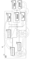
- FIG. 10 is a block diagram showing the configuration of a vehicle 60 equipped with a backup power supply device 10c according to a third modified embodiment.
- the vehicle 60 includes components related to the backup power supply device 10c, such as a vehicle power source 55, such as a lead battery used to charge the backup power supply device 10c, an alternator generator 56, and door ECUs (Electronic Control Units)/ACTs 50a-50c as loads 50, a steering device 50d, and a brake device 50e.
- a vehicle power source 55 such as a lead battery used to charge the backup power supply device 10c
- an alternator generator 56 such as a lead battery used to charge the backup power supply device 10c
- door ECUs (Electronic Control Units)/ACTs 50a-50c as loads 50
- a steering device 50d a steering device 50d
- brake device 50e brake device
- FIG. 11 is a block diagram showing the configuration of the backup power supply device 10c in FIG. 10. Also shown here is a vehicle power supply 55 and a load 50.
- the backup power supply device 10c has a configuration in which, instead of the unidirectional first DC/DC converter 12 and the first control circuit 15 that controls it in the backup power supply device 10 according to the embodiment, a bidirectional first DC/DC converter 12a and a first control circuit 15a that controls it are provided, and an interrupting element 28 and a backup detection circuit 29 are added.
- a bidirectional first DC/DC converter 12a and a first control circuit 15a that controls it are provided, and an interrupting element 28 and a backup detection circuit 29 are added.
- the first DC/DC converter 12a is a bidirectional DC/DC converter and has the same function as the second DC/DC converter 14.
- the first control circuit 15a is a circuit that controls the first DC/DC converter 12a and has the same function as the second control circuit 16.
- the interrupting element 28 is a circuit breaker that turns on/off the connection between the vehicle power supply 55 and the backup power supply device 10c, more specifically, the connection between the vehicle power supply 55 and the first current detection circuit 17.
- the backup detection circuit 29 is a control circuit that monitors the output voltage of the vehicle power supply 55, and if the output voltage falls below a threshold, turns off the cutoff element 28, and if not, turns on the cutoff element 28.
- FIG. 12 is a diagram showing the flow of current in the vehicle power supply mode of the backup power supply device 10c shown in FIG. 11.
- the backup detection circuit 29 turns off the cutoff element 28, and the same operation as the backup power supply device 10 of the embodiment is performed, that is, the normal current mode in which current is supplied from the first storage element 11 to the load 50, or the high current mode in which current is supplied from the first storage element 11 and the second storage element 13 to the load 50 is performed.
- the backup power supply device 10c of this modified example in the vehicle power supply mode where the output voltage of the vehicle power supply 55 is equal to or higher than the threshold value, current is supplied from the vehicle power supply 55 to the load 50, and current is also supplied to the first storage element 11 and the second storage element 13.
- the backup power supply mode where the output voltage of the vehicle power supply 55 is lower than the threshold value current is supplied from the backup power supply device 10c to the load 50 in the normal current mode or the large current mode.
- the backup power supply device 10a according to the first modified example has a configuration in which the first switch 24, the second switch 25, the third DC/DC converter 21, etc. are added to the configuration of the backup power supply device 10 according to the embodiment, but this is not limited to this, and the backup power supply device 10b according to the second modified example or the backup power supply device 10c according to the third modified example may have a configuration in which the first switch 24, the second switch 25, the third DC/DC converter 21, etc. are added to the configuration.
- the present disclosure can be used as a power supply device and a vehicle equipped with a power supply device, for example, as a backup power supply device that is not restricted by the combination of two storage elements, and as a vehicle equipped with such a backup power supply device.
Landscapes
- Engineering & Computer Science (AREA)
- Power Engineering (AREA)
- Chemical & Material Sciences (AREA)
- Combustion & Propulsion (AREA)
- Transportation (AREA)
- Mechanical Engineering (AREA)
- Charge And Discharge Circuits For Batteries Or The Like (AREA)
Priority Applications (1)
| Application Number | Priority Date | Filing Date | Title |
|---|---|---|---|
| JP2025531491A JPWO2025009417A1 (https=) | 2023-07-06 | 2024-06-21 |
Applications Claiming Priority (2)
| Application Number | Priority Date | Filing Date | Title |
|---|---|---|---|
| JP2023111133 | 2023-07-06 | ||
| JP2023-111133 | 2023-07-06 |
Publications (1)
| Publication Number | Publication Date |
|---|---|
| WO2025009417A1 true WO2025009417A1 (ja) | 2025-01-09 |
Family
ID=94171717
Family Applications (1)
| Application Number | Title | Priority Date | Filing Date |
|---|---|---|---|
| PCT/JP2024/022596 Ceased WO2025009417A1 (ja) | 2023-07-06 | 2024-06-21 | 電源装置及び車両 |
Country Status (2)
| Country | Link |
|---|---|
| JP (1) | JPWO2025009417A1 (https=) |
| WO (1) | WO2025009417A1 (https=) |
Citations (3)
| Publication number | Priority date | Publication date | Assignee | Title |
|---|---|---|---|---|
| JP2013099188A (ja) * | 2011-11-04 | 2013-05-20 | Sharp Corp | 電力変換装置、蓄電システムおよびその制御方法 |
| JP2016116258A (ja) * | 2014-12-11 | 2016-06-23 | トヨタ自動車株式会社 | 電源制御装置 |
| WO2020161765A1 (ja) * | 2019-02-04 | 2020-08-13 | Tdk株式会社 | 直流給電システム |
-
2024
- 2024-06-21 JP JP2025531491A patent/JPWO2025009417A1/ja active Pending
- 2024-06-21 WO PCT/JP2024/022596 patent/WO2025009417A1/ja not_active Ceased
Patent Citations (3)
| Publication number | Priority date | Publication date | Assignee | Title |
|---|---|---|---|---|
| JP2013099188A (ja) * | 2011-11-04 | 2013-05-20 | Sharp Corp | 電力変換装置、蓄電システムおよびその制御方法 |
| JP2016116258A (ja) * | 2014-12-11 | 2016-06-23 | トヨタ自動車株式会社 | 電源制御装置 |
| WO2020161765A1 (ja) * | 2019-02-04 | 2020-08-13 | Tdk株式会社 | 直流給電システム |
Also Published As
| Publication number | Publication date |
|---|---|
| JPWO2025009417A1 (https=) | 2025-01-09 |
Similar Documents
| Publication | Publication Date | Title |
|---|---|---|
| US10017138B2 (en) | Power supply management system and power supply management method | |
| JP2000197347A (ja) | 電源装置 | |
| JP2002171692A (ja) | 直流電源装置 | |
| CN106476635A (zh) | 具有多个能量存储装置的混合系统 | |
| JP2007336664A (ja) | 2次電池充電回路 | |
| CN115051423B (zh) | 充放电控制装置 | |
| CN111404399B (zh) | 供电系统 | |
| JP2010016996A (ja) | 無停電電源装置 | |
| JP6969505B2 (ja) | 車載用の電源制御装置および車載用電源システム | |
| CN112041200A (zh) | 车载用的备用电路及车载用的备用装置 | |
| WO2021241136A1 (ja) | バックアップ電源装置 | |
| JP6971602B2 (ja) | レンジエクステンダーおよび回路保護方法 | |
| JP2007236064A (ja) | 蓄電装置 | |
| JP5304279B2 (ja) | 蓄電装置 | |
| JP5073436B2 (ja) | 無瞬断バックアップ電源 | |
| US20090315402A1 (en) | Ac-dc conversion device | |
| JP7565001B2 (ja) | 車載用制御装置 | |
| CN110739765B (zh) | 直流供电系统 | |
| WO2025009417A1 (ja) | 電源装置及び車両 | |
| JP2000323365A (ja) | 直流給電装置 | |
| JP2022011203A (ja) | バックアップ電源装置及びバックアップ電源装置の制御方法 | |
| JP2009055701A (ja) | 電源装置 | |
| JP4774961B2 (ja) | 無停電電源装置 | |
| US20220368215A1 (en) | Power conversion system for electrically driven mobility device and method for controlling same | |
| JP3954081B1 (ja) | 蓄電装置 |
Legal Events
| Date | Code | Title | Description |
|---|---|---|---|
| 121 | Ep: the epo has been informed by wipo that ep was designated in this application |
Ref document number: 24835930 Country of ref document: EP Kind code of ref document: A1 |
|
| ENP | Entry into the national phase |
Ref document number: 2025531491 Country of ref document: JP Kind code of ref document: A |
|
| WWE | Wipo information: entry into national phase |
Ref document number: 2025531491 Country of ref document: JP |
|
| NENP | Non-entry into the national phase |
Ref country code: DE |