WO2025009348A1 - 積層セラミックコンデンサ - Google Patents
積層セラミックコンデンサ Download PDFInfo
- Publication number
- WO2025009348A1 WO2025009348A1 PCT/JP2024/021452 JP2024021452W WO2025009348A1 WO 2025009348 A1 WO2025009348 A1 WO 2025009348A1 JP 2024021452 W JP2024021452 W JP 2024021452W WO 2025009348 A1 WO2025009348 A1 WO 2025009348A1
- Authority
- WO
- WIPO (PCT)
- Prior art keywords
- glass
- electrode layer
- multilayer ceramic
- ceramic capacitor
- base electrode
- Prior art date
- Legal status (The legal status is an assumption and is not a legal conclusion. Google has not performed a legal analysis and makes no representation as to the accuracy of the status listed.)
- Ceased
Links
Images


Classifications
-
- H—ELECTRICITY
- H01—ELECTRIC ELEMENTS
- H01G—CAPACITORS; CAPACITORS, RECTIFIERS, DETECTORS, SWITCHING DEVICES, LIGHT-SENSITIVE OR TEMPERATURE-SENSITIVE DEVICES OF THE ELECTROLYTIC TYPE
- H01G4/00—Fixed capacitors; Processes of their manufacture
- H01G4/002—Details
- H01G4/228—Terminals
- H01G4/232—Terminals electrically connecting two or more layers of a stacked or rolled capacitor
- H01G4/2325—Terminals electrically connecting two or more layers of a stacked or rolled capacitor characterised by the material of the terminals
-
- H—ELECTRICITY
- H01—ELECTRIC ELEMENTS
- H01G—CAPACITORS; CAPACITORS, RECTIFIERS, DETECTORS, SWITCHING DEVICES, LIGHT-SENSITIVE OR TEMPERATURE-SENSITIVE DEVICES OF THE ELECTROLYTIC TYPE
- H01G4/00—Fixed capacitors; Processes of their manufacture
- H01G4/30—Stacked capacitors
Definitions
- This disclosure relates to multilayer ceramic capacitors.
- the external electrodes of a multilayer ceramic capacitor generally include a base electrode layer formed on the surface of a laminate such as a ceramic body, and a plating layer applied onto the base electrode layer.
- the base electrode layer is often formed from a conductive paste containing glass to achieve densification.
- the glass used in the base electrode layer is designed to satisfy various required properties, such as filling pores inside the external electrode to form a dense film, acting as an auxiliary agent in the sintering process, adhering to the body after firing, and having chemical durability of the glass itself.
- Multilayer ceramic capacitors are prone to solder explosions when the base electrode layer of the external electrodes contains glass. Solder explosions occur when, for example, a multilayer ceramic capacitor is mounted on a circuit board and fixed by soldering, and the heat of soldering causes moisture or plating solution that has penetrated into the base electrode layer to rapidly evaporate, causing the solder on the outer layer to fly off, which can result in a short circuit.
- the objective of this disclosure is to provide a multilayer ceramic capacitor with external electrodes that suppress solder explosions.
- the multilayer ceramic capacitor according to the present disclosure comprises an external electrode and a laminate including a plurality of laminated dielectric layers and a plurality of internal electrode layers.
- the external electrode includes a plating layer and a base electrode layer.
- the base electrode layer includes glass.
- the glass includes an alkaline earth metal. In the thickness direction of the base electrode layer, when the mass ratio of the alkaline earth metal in the glass present in the center is taken as 100, the mass ratio of the alkaline earth metal in the glass present near the surface on the plating layer side is 90 or more and less than 100.
- This disclosure makes it possible to provide a multilayer ceramic capacitor with external electrodes that suppress solder explosions.
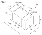
- FIG. 1 is a perspective view showing the appearance of a multilayer ceramic capacitor according to the present disclosure.
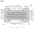
- 2 is a cross-sectional view of the multilayer ceramic capacitor of FIG. 1, taken along the line II-II.
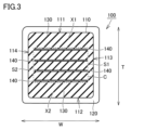
- 3 is a cross-sectional view of the multilayer ceramic capacitor of FIG. 1 as viewed from the direction of the arrows indicated by the line III-III.
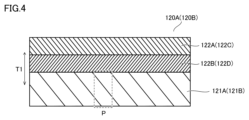
- FIG. 4 is a cross-sectional view showing the layer structure of the external electrodes.
- FIG. 5 is a schematic diagram for explaining the fine structure of the base electrode layer.
- FIG. 6 is a cross-sectional view for explaining the central portion, the surface vicinity, and the interface vicinity of the base electrode layer.
- the multilayer ceramic capacitor includes an external electrode and a laminate including a plurality of laminated dielectric layers and a plurality of internal electrode layers, the external electrode being disposed on the laminate with the base electrode layer side.
- FIG. 1 is a perspective view showing the appearance of the multilayer ceramic capacitor of the present disclosure.
- FIG. 2 is a cross-sectional view of the multilayer ceramic capacitor of FIG. 1 as viewed from the direction of the arrows along line II-II.
- FIG. 3 is a cross-sectional view of the multilayer ceramic capacitor of FIG. 1 as viewed from the direction of the arrows along line III-III.
- the laminated ceramic capacitor 100 of the present disclosure includes a laminate 110 and an external electrode 120.
- the laminate 110 includes a plurality of dielectric layers 130 and a plurality of internal electrode layers 140 that are alternately stacked one by one along the stacking direction T.
- the laminate 110 has a first main surface 111 and a second main surface 112 that face each other in the stacking direction, a first side surface 113 and a second side surface 114 that face each other in the width direction perpendicular to the stacking direction, and a first end surface 115 and a second end surface 116 that face each other in the length direction perpendicular to the stacking direction and the width direction.
- the laminate 110 is divided into an inner layer portion C, a first outer layer portion X1, a second outer layer portion X2, a first side margin portion S1, a second side margin portion S2, a first end margin portion E1, and a second end margin portion E2.
- the external electrode 120 is provided on the surface of the laminate 110.
- the external electrode 120 includes a base electrode layer 121 and a plating layer 122.
- the external electrode 120 can be composed of a first external electrode 120A and a second external electrode 120B.
- the first external electrode 120A is provided on the first end face 115.
- the second external electrode 120B is provided on the second end face 116.
- the first external electrode 120A is formed on the first end face 115 of the laminate 110 so as to be electrically connected to the first internal electrode layer 140A, and extends from the first end face 115 to the first main surface 111 and the second main surface 112 as well as the first side surface and the second side surface.
- the second external electrode 120B is formed on the second end face 116 of the laminate 110 so as to be electrically connected to the second internal electrode layer 140B, and extends from the second end face 116 to the first main surface 111 and the second main surface 112 as well as the first side surface and the second side surface.
- the first external electrode 120A (second external electrode 120B) has a first base electrode layer 121A (second base electrode layer 121B), a first lower plating layer 122B (second lower plating layer 122D) arranged on the first base electrode layer 121A (second base electrode layer 121B), and a first upper plating layer 122A (second upper plating layer 122C) arranged on the first lower plating layer 122B (second lower plating layer 122D).
- FIG. 5 is a schematic diagram for explaining the microstructure of the base electrode layer 121.
- the base electrode layer 121 includes glass 150.
- the base electrode layer can be a sintered layer of a conductive paste including a glass composition. The conductive paste will be described later.
- the glass 150 may include, for example, borosilicate glass, which is glass that includes boron oxide (B 2 O 3 ) and silicon oxide (SiO 2 ) as network-forming oxides.
- borosilicate glass which is glass that includes boron oxide (B 2 O 3 ) and silicon oxide (SiO 2 ) as network-forming oxides.
- Glass 150 includes an alkaline earth metal.
- the alkaline earth metal may include at least one element selected from the group consisting of calcium (Ca), strontium (Sr), and barium (Ba).
- the alkaline earth metal may further include magnesium (Mg).
- the alkaline earth metal may be included in glass 150 as a network-modifying oxide (e.g., CaO, SrO, BaO, MgO, etc.).
- the mass ratio of the alkaline earth metal in the glass present in the center (hereinafter also referred to as the first ratio) is 100
- the mass ratio of the alkaline earth metal in the glass present near the surface on the plating layer side (hereinafter also referred to as the second ratio) is 90 or more and less than 100.
- the mass ratio of the alkaline earth metal in the glass is the mass ratio of the alkaline earth metal contained in the glass based on the mass of the glass.
- the mass ratio of the alkaline earth metal in the glass is measured according to the method described in the Examples section below.
- Figure 6 is an enlarged cross-sectional view of region P surrounded by a dotted line in the base electrode layer shown in Figure 4.
- regions 1 and 2 are referred to as the vicinity of the surface
- regions 3 to 8 are referred to as the central portion.
- the mass ratio of alkaline earth metals in the glass present near the surface of the base electrode layer tends to be lower than the mass ratio of alkaline earth metals in the glass present in the center. It is presumed that this is because, in the plating process to form the plating layer, the base electrode layer comes into contact with water or plating solution, causing the alkaline earth metals in the glass to dissolve into the plating solution, and other components also move along with it, changing the composition of the glass.
- the mass ratio of alkaline earth metals in the glass present near the surface decreases, the glass is eroded, and moisture and plating solution easily penetrate into the base electrode layer, making it easier for solder explosions to occur.
- the difference in the content of alkaline earth metals in the glass present in the center and near the surface on the plating layer side in the thickness direction of the base electrode layer is small, so solder explosions are easily suppressed. The ease of suppressing solder explosions is evaluated according to the method described in the Examples section below.
- the second ratio is preferably 96 or more from the viewpoint of suppressing solder explosion.
- the second ratio may be, for example, 98 or less.
- the base electrode layer 121 preferably has a mass ratio of alkaline earth metal in the glass present in region 1 of 90 or more and less than 100 when the mass ratio of alkaline earth metal in the glass present in region 6 is taken as 100.
- the base electrode layer 121 can have a mass ratio (hereinafter also referred to as the third ratio) of the alkaline earth metal in the glass present near the surface on the laminate 110 side (hereinafter also referred to as the interface vicinity) of 105 to 115.
- the third ratio in the above range, it tends to be easier to suppress a decrease in the strength of the laminate described below.
- the interface vicinity is the above-mentioned region 9 to 10.
- the third ratio is preferably 112 or less from the viewpoint of preventing a decrease in strength of the laminate.
- the glass 150 may further include an alkali metal.
- the alkali metal may be, for example, at least one element selected from lithium (Li), sodium (Na), and potassium (K).
- the alkali metal may be included in the glass 150 as a network modifier oxide (for example, Li 2 O, Na 2 O, K 2 O).
- the glass 150 may contain oxides other than those mentioned above, such as oxides of transition metal elements, zinc oxide (ZnO), aluminum oxide (Al 2 O 3 ), and bismuth oxide (Bi 2 O 3 ).
- the glass 150 may further contain a metal oxide, such as copper oxide (CuO).
- a metal oxide such as copper oxide (CuO).
- the base electrode layer 121 may further contain at least one conductive component selected from the group consisting of copper (Cu), nickel (Ni) and a Cu-Ni alloy.
- the conductive component may be a conductive powder.
- the conductive component may be contained in a region 151 other than the glass 150 (hereinafter also referred to as a conductive region).
- the conductive region 151 may include a metal sintered body formed by sintering conductive powder contained in the conductive paste.
- the thickness of the base electrode layer 121 may be, for example, 10 ⁇ m or more and 50 ⁇ m or less, and preferably 15 ⁇ m or more and 40 ⁇ m or less.
- the thickness of the base electrode layer 121 is measured as follows. First, the multilayer ceramic capacitor 100 is polished to expose a cross section perpendicular to the width direction W. The exposed cross section is observed and measured using a microscope. The measurement position is the center of the stacking direction T.
- the base electrode layer 121 tends to become thinner near the ends formed on the first main surface 111, the second main surface 112, the first side surface 113, and the second side surface 114, and is easily affected by the plating solution.
- the alkaline earth metal content of the glass contained in the base electrode layer 121 be the first ratio and the second ratio described above, solder explosion can be suppressed even near the ends where the thickness tends to become thinner.
- the plating layer 122 may include, for example, nickel (Ni), Cu, silver (Ag), gold (Au), and tin (Sn), or an alloy containing these metals.
- the plating layer 122 may be formed of multiple layers of different components.
- the plating layer 122 may have a two-layer structure consisting of an upper plating layer (the first upper plating layer 122A and the second upper plating layer 122C are also collectively referred to as the upper plating layer) and a lower plating layer (the first lower plating layer 122B and the second lower plating layer 122D are also collectively referred to as the upper plating layer).
- the lower plating layers are each disposed on the base electrode layer, and can prevent the base electrode layer from being eroded by solder when mounting the multilayer ceramic capacitor.
- the lower plating layer may be, for example, a Ni plating layer.
- the upper plating layer is disposed on the lower plating layer.
- the upper plating layer may be, for example, a Sn plating layer.
- the Sn plating layer has good wettability with solder containing Sn, which improves mounting properties when mounting multilayer ceramic capacitors.
- the upper and lower plating layers may be, for example, 0.5 ⁇ m or more and 10 ⁇ m or less, preferably 5.5 ⁇ m or less, and more preferably 4.5 ⁇ m or less.
- the thickness of each of the upper and lower plating layers is measured as follows. First, the multilayer ceramic capacitor 100 is polished using an FIB device to expose a cross section perpendicular to the width direction W. The exposed cross section is observed under a microscope, and the thickness of each of the above layers is measured. The measurement position is the center of the stacking direction T. The thickness of the upper plating layer may also be measured using a fluorescent X-ray film thickness gauge.
- the dielectric layer 130 has a plurality of crystal grains including, for example, a BaTiO 3 -based perovskite compound.
- the dielectric material may be, for example, a BaTiO 3 -based perovskite compound in which a part of the Ba 2+ in the crystal lattice is replaced by Re 3+ , which is a rare earth element ion.
- the BaTiO 3 -based perovskite compound include BaTiO 3 and BaTiO 3 in which at least one of Ba 2+ and Ti 4+ is replaced by other ions such as Ca 2+ and Zr 4+ .
- each of the multiple dielectric layers 130 included in the inner layer portion C is preferably 0.4 ⁇ m or more and 0.8 ⁇ m or less, and more preferably 0.5 ⁇ m or more and 0.7 ⁇ m or less. In this specification, the thickness of each layer is the thickness at the center of the end face.
- the multiple internal electrode layers 140 include multiple first internal electrode layers 140A connected to the first external electrode 120A, and multiple second internal electrode layers 140B connected to the second external electrode 120B.
- the first internal electrode layer 140A has an opposing electrode portion 141A that faces the second internal electrode layer 140B through the dielectric layer 130, and an extraction electrode portion 142A from the opposing electrode portion 141A to the first end surface 115 of the laminate 110.
- the second internal electrode layer 140B has an opposing electrode portion 141B that faces the first internal electrode layer 140A through the dielectric layer 130, and an extraction electrode portion 142B from the opposing electrode portion 141B to the second end surface 116 of the laminate 110.
- a single capacitor is formed by the first internal electrode layer 140A and the second internal electrode layer 140B facing each other via the dielectric layer 130.
- the multilayer ceramic capacitor 100 can be said to be a plurality of capacitors connected in parallel via the first external electrode 120A and the second external electrode 120B.
- the conductive material constituting the internal electrode layer 140 may be at least one metal selected from the group consisting of Ni, Cu, Ag, and palladium (Pd), or an alloy containing such a metal.
- the internal electrode layer 140 may further contain dielectric particles called a common material.
- each of the multiple internal electrode layers 140 is preferably 0.3 ⁇ m or more and 1.0 ⁇ m or less.
- the coverage rate of each of the multiple internal electrode layers 140 covering the dielectric layer 130 without gaps is preferably 50% or more and 95% or less.
- the thickness of each of the dielectric layers 130 and the internal electrode layers 140 included in the inner layer portion C is measured as follows. First, the multilayer ceramic capacitor 100 is polished to expose a cross section perpendicular to the length direction L. The exposed cross section is observed with a scanning electron microscope. Next, the thickness of each of the dielectric layers 130 and the internal electrode layers 140 is measured on a total of five lines, including a center line along the stacking direction T that passes through the center of the exposed cross section, and two lines drawn equally spaced on each side of this center line. The average of the five measured values of the dielectric layer 130 is defined as the thickness of the dielectric layer 130. The average of the five measured values of the internal electrode layer 140 is defined as the thickness of the internal electrode layer 140.
- the thicknesses of the dielectric layer 130 and the internal electrode layer 140 on the above-mentioned five lines may be measured at the upper, central, and lower parts located on the boundary lines dividing the exposed cross section into four equal parts in the stacking direction T, and the average value of the measured values of the dielectric layer 130 may be regarded as the thickness of the dielectric layer 130, and the average value of the measured values of the internal electrode layer 140 may be regarded as the thickness of the internal electrode layer 140.
- the first outer layer X1 and the second outer layer X2 are respectively disposed between the first main surface 111 of the laminate 110 and the internal electrode layer 140 closest to the first main surface 111, and between the second main surface 112 and the internal electrode layer 140 closest to the second main surface 112.
- the internal layer C is disposed in the region sandwiched between the two first outer layer X1 and second outer layer X2.
- the inner layer portion C has a capacitance due to the opposing electrode portion 141A of the first internal electrode layer 140A and the opposing electrode portion 141B of the second internal electrode layer 140B being stacked in the stacking direction T.
- the first outer layer portion X1 is located on the first main surface 111 side of the inner layer portion C in the stacking direction T.
- the second outer layer portion X2 is located on the second main surface 112 side of the inner layer portion C in the stacking direction T.
- the first side margin portion S1 is located on the first side surface 113 side of the inner layer portion C in the width direction W.
- the second side margin portion S2 is located on the second side surface 114 side of the inner layer portion C in the width direction W.
- the first end margin portion E1 is located on the first end surface 115 side of the inner layer portion C in the length direction L.
- the second end margin portion E2 is located on the second end surface 116 side of the inner layer portion C in the length direction L.
- the dimension in the width direction W of the first side margin portion S1, the dimension in the width direction W of the second side margin portion S2, the dimension in the length direction L of the first end margin portion E1, and the dimension in the length direction L of the second end margin portion E2 are each small enough so that the insulation resistance of the multilayer ceramic capacitor 100 is not reduced.
- the multilayer ceramic capacitor 100 has a length direction L dimension of 2.0 mm or less, a width direction W dimension of 1.25 mm or less, and a stacking direction T dimension of 1.25 mm or less.
- the external dimensions of the multilayer ceramic capacitor 100 can be measured by observing the multilayer ceramic capacitor 100 with an optical microscope.
- a ceramic slurry is first prepared. Specifically, ceramic powder, a binder, a solvent, etc. are mixed in a predetermined ratio to form the ceramic slurry.
- a ceramic green sheet is formed. Specifically, the ceramic slurry is formed into a sheet on a carrier film using a die coater, gravure coater, or microgravure coater, etc., to form a ceramic green sheet.
- a mother sheet is formed. Specifically, a conductive paste is printed onto the ceramic green sheet in a predetermined pattern using a screen printing method, a gravure printing method, or the like, to form a mother sheet having a predetermined conductive pattern on the ceramic green sheet.
- ceramic green sheets without a conductive pattern are also prepared as mother sheets.
- the mother sheets are stacked. Specifically, a predetermined number of mother sheets that do not have a conductive pattern and that form the first outer layer portion X1 are stacked, and then a plurality of mother sheets that have a conductive pattern and that form the inner layer portion C are stacked in sequence on top of these, and then a predetermined number of mother sheets that do not have a conductive pattern and that form the second outer layer portion X2 are stacked on top of these to form a mother sheet group.
- the mother sheets are pressed together.
- the mother sheets are pressed together in the stacking direction by a hydrostatic press or a rigid press to form a mother laminate.
- the mother laminate is divided. Specifically, the mother laminate is divided into a matrix shape by pressing or dicing, and is divided into a number of individual unfired laminates.
- the unsintered laminate is barrel polished. Specifically, the unsintered laminate is enclosed in a small box called a barrel together with media balls that are harder than the ceramic material, and the corners and edges of the unsintered laminate are rounded by rotating the barrel.
- the unsintered laminate is fired. Specifically, the unsintered laminate is heated to a predetermined temperature, thereby firing the dielectric ceramic material.
- the firing temperature is set appropriately depending on the type of dielectric ceramic material, and is set, for example, within the range of 900°C to 1300°C.
- a base electrode layer is formed on the surface of the laminate.
- the base electrode layer 121 is formed by various thin film formation methods, various printing methods, a dip method, or the like.
- a conductive paste is applied to the first end face and the second end face of the laminate, and then dried and the conductive paste is baked.
- the baking temperature is set, for example, within the range of 700°C to 800°C.
- the base electrode layer can be a sintered layer of a conductive paste.
- the conductive paste may contain a glass composition, a conductive component, and an organic component.
- the glass composition may be in a powder state.
- the organic component may contain, for example, a vehicle and an additive.
- the vehicle may contain, for example, a resin and an organic solvent.
- the additive may contain, for example, a dispersant and a rheology control agent.
- the organic material may be appropriately selected from materials that are typically used as organic materials for conductive pastes.
- the glass composition contained in the conductive paste when expressed in terms of composition by mass percentage, can contain 0 to 2 mass% Li 2 O, 0 to 8 mass% Na 2 O, 1 to 8 mass% CaO, 0 to 8 mass% SrO, 20 to 60 mass% BaO, 16 to 28 mass% B 2 O 3 , 5 to 12 mass% SiO 2 , 12 to 20 mass% Al 2 O 3 , 0 to 4.0 mass% TiO 2 , and 0 to 5.0 mass% CuO, the total of which amounts to 100 mass%.
- the glass composition contained in the conductive paste when the composition is expressed in mass percentage, can preferably contain 0 to 2 mass% Li 2 O, 0 to 8 mass% Na 2 O, 1 to 8 mass% CaO, 0 to 8 mass% SrO, 20 to 50 mass% BaO, 19 to 28 mass% B 2 O 3 , 5 to 12 mass% SiO 2 , 12 to 20 mass% Al 2 O 3 , 2.5 to 4.0 mass% TiO 2 , and 0 to 5.0 mass% CuO in a total range of 100 mass%.
- the mass ratio of the total of Li 2 O, Na 2 O, CaO and BaO to B 2 O 3 is preferably 1.17 to 2.61.
- a lower plating layer and an upper plating layer are successively formed by electrolytic plating so as to cover the base electrode layer by a plating process.
- the plating layers may be formed by electrolytic plating using a barrel electroplating device.
- the base electrode layer may be subjected to a surface treatment, such as sandblasting or water repellent treatment. The formation of each of the above electrodes constitutes an external electrode.
- the multilayer ceramic capacitor 100 of the present disclosure is manufactured.
- a conductive paste was prepared by mixing a glass composition having the composition shown in Table 1 with an organic component.
- the prepared conductive paste was applied to a first end face and a second end face of a laminate including a plurality of laminated dielectric layers and a plurality of internal electrode layers, dried, and then baked. After polishing (sandblasting, water repellent treatment) was performed on the surface of the external electrode, a Ni plating layer was formed, and then a Sn plating layer was formed to prepare a multilayer ceramic capacitor. The results are shown in Table 1.
- Composition 1 and Composition 2 have the following compositions.
- Composition 1 It contains 0-2 mass% Li 2 O, 0-8 mass% Na 2 O, 1-8 mass% CaO, 0-8 mass% SrO, 20-60 mass% BaO, 16-28 mass% B 2 O 3 , 5-12 mass% SiO 2 , 12-20 mass% Al 2 O 3 , 2.5-4.0 mass% TiO 2 , and 0-5.0 mass% CuO, the total of which is 100 mass%.
- composition 2 It contains 0-2 mass% Li 2 O, 0-8 mass% Na 2 O, 1-8 mass% CaO, 0-8 mass% SrO, 20-50 mass% BaO, 19-28 mass% B 2 O 3 , 5-12 mass% SiO 2 , 12-20 mass% Al 2 O 3 , 2.5-4.0 mass% TiO 2 , and 0-5.0 mass% CuO, the total of which is 100 mass%.
- the multilayer ceramic capacitor of the present disclosure comprises an external electrode and a laminate including a plurality of laminated dielectric layers and a plurality of internal electrode layers.
- the external electrode includes a plating layer and a base electrode layer.
- the base electrode layer includes glass.
- the glass includes an alkaline earth metal. In the thickness direction of the base electrode layer, when the mass ratio of the alkaline earth metal in the glass present in the center is taken as 100, the mass ratio of the alkaline earth metal in the glass present near the surface on the plating layer side is 90 or more and less than 100.
- the base electrode layer of the multilayer ceramic capacitor of 1 has a mass ratio of alkaline earth metal in the glass present near the surface on the plating layer side of 96 to 98.
- the glass contains borosilicate glass.
- the glass further contains an alkali metal.
- the glass further contains copper oxide.
- the base electrode layer further contains at least one conductive component selected from the group consisting of copper, nickel, and copper-nickel alloy.
- the base electrode layer is a sintered layer of a conductive paste containing a glass composition.
- the glass composition contains Li 2 O, Na 2 O, CaO, BaO and B 2 O 3.
- the mass ratio of the total of Li 2 O, Na 2 O, CaO and BaO to B 2 O 3 in the glass composition is 1.17 to 2.61.
Landscapes
- Engineering & Computer Science (AREA)
- Power Engineering (AREA)
- Manufacturing & Machinery (AREA)
- Microelectronics & Electronic Packaging (AREA)
- Ceramic Capacitors (AREA)
- Fixed Capacitors And Capacitor Manufacturing Machines (AREA)
Abstract
本開示の積層セラミックコンデンサは、外部電極と、積層された複数の誘電体層及び複数の内部電極層を含む積層体とを備える。外部電極は、めっき層と、下地電極層とを含む。下地電極層は、ガラスを含む。ガラスは、アルカリ土類金属を含む。下地電極層は、厚み方向において、中央部に存在する前記ガラス中のアルカリ土類金属の質量割合を100としたとき、めっき層側の表面付近に存在するガラス中のアルカリ土類金属の質量割合が90以上100未満である。
Description
本開示は、積層セラミックコンデンサに関する。
特許文献1に記載のように、積層セラミックコンデンサの外部電極は一般に、セラミック素体等の積層体の表面に形成された下地電極層と、下地電極層上に付与されためっき層とを含む。下地電極層は、緻密化のために、ガラスを含む導電性ペーストから形成される場合が多い。下地電極層に用いられるガラスは、外部電極の内部においてポアを埋めて緻密な膜を作ることに加えて、焼結過程での助剤として働くこと、焼付け後に素体と固着すること、及びガラス自体が化学的耐久性を持つことといった種々の要求特性を満たすように設計される。
積層セラミックコンデンサは、外部電極の下地電極層がガラスを含む場合、はんだ爆ぜが生じ易い傾向にある。はんだ爆ぜは、例えば積層セラミックコンデンサを回路基板に装着し、はんだ付けで固定する際、はんだ付けの熱により、下地電極層に入り込んだ水分やめっき液が急速に蒸発し、外層のはんだが飛ぶ現象であり、短絡不良の発生するおそれがある。
本開示の目的は、はんだ爆ぜが抑制された外部電極を備えた積層セラミックコンデンサを提供することである。
本開示に基づく積層セラミックコンデンサは、外部電極と、積層された複数の誘電体層及び複数の内部電極層を含む積層体とを備える。外部電極は、めっき層と、下地電極層とを含む。下地電極層は、ガラスを含む。ガラスは、アルカリ土類金属を含む。下地電極層は、厚み方向において、中央部に存在するガラス中のアルカリ土類金属の質量割合を100としたとき、めっき層側の表面付近に存在するガラス中のアルカリ土類金属の質量割合が90以上100未満である。
本開示によれば、はんだ爆ぜが抑制された外部電極を備える積層セラミックコンデンサを提供することができる。
以下、本開示の積層セラミックコンデンサについて図を参照して説明する。以下の各実施形態の説明においては、図中の同一又は相当部分には同一符号を付して、その説明は繰り返さない。
<積層セラミックコンデンサ>
積層セラミックコンデンサは、外部電極と、積層された複数の誘電体層と複数の内部電極層とを含む積層体とを備える。外部電極は、下地電極層側が積層体上に配置される。
積層セラミックコンデンサは、外部電極と、積層された複数の誘電体層と複数の内部電極層とを含む積層体とを備える。外部電極は、下地電極層側が積層体上に配置される。
図1は、本開示の積層セラミックコンデンサの外観を示す斜視図である。図2は、図1の積層セラミックコンデンサをII-II線矢印方向から見た断面図である。図3は、図1の積層セラミックコンデンサをIII-III線矢印方向から見た断面図である。
図1から図3に示すように、本開示の積層セラミックコンデンサ100は、積層体110と、外部電極120とを備える。図2及び図3に示すように、積層体110は、積層方向Tに沿って1層ずつ交互に積層された複数の誘電体層130及び複数の内部電極層140を含んでいる。積層体110は、積層方向に相対する第1の主面111及び第2の主面112と、積層方向に直交する幅方向に相対する第1の側面113及び第2の側面114と、積層方向及び幅方向に直交する長さ方向に相対する第1の端面115及び第2の端面116とを有する。積層体110は、内層部Cと第1の外層部X1と第2の外層部X2と、第1のサイドマージン部S1と第2のサイドマージン部S2と第1のエンドマージン部E1と第2のエンドマージン部E2とに区画される。
図1から図3に示すように、外部電極120は、積層体110の表面に設けられている。図2に示すように、外部電極120は、下地電極層121と、めっき層122とを含む。外部電極120は、第1の外部電極120Aと、第2の外部電極120Bとから構成されることができる。第1の外部電極120Aは、第1の端面115に設けられている。第2の外部電極120Bは、第2の端面116に設けられている。
第1の外部電極120Aは、第1の内部電極層140Aと電気的に接続されるように積層体110の第1の端面115に形成され、第1の端面115から第1の主面111及び第2の主面112ならびに第1の側面及び第2の側面延びている。第2の外部電極120Bは、第2の内部電極層140Bと電気的に接続されるように積層体110の第2の端面116に形成され、第2の端面116から第1の主面111及び第2の主面112ならびに第1の側面及び第2の側面に延びている。
図4に示すように、第1の外部電極120A(第2の外部電極120B)は、第1の下地電極層121A(第2の下地電極層121B)と、第1の下地電極層121A(第2の下地電極層121B)上に配置された第1の下側めっき層122B(第2の下側めっき層122D)と、第1の下側めっき層122B(第2の下側めっき層122D)上に配置された第1の上側めっき層122A(第2の上側めっき層122C)とを有する。
図5は、下地電極層121の微細構造を説明するための模式図である。図5に示すように、下地電極層121はガラス150を含む。下地電極層は、ガラス組成物を含む導電性ペーストの焼結体層であることができる。導電性ペーストについては後述する。
ガラス150は、例えばホウケイ酸系ガラスを含むことができる。ホウケイ酸系ガラスは、ホウ素酸化物(B2O3)及びケイ素酸化物(SiO2)を網目形成酸化物として含むガラスである。
ガラス150は、アルカリ土類金属を含む。アルカリ土類金属は、例えばカルシウム(Ca)、ストロンチウム(Sr)及びバリウム(Ba)からなる群から選択される少なくとも1種の元素を含むことができる。アルカリ土類金属は、マグネシウム(Mg)をさらに含んでいてもよい。アルカリ土類金属は、網目修飾酸化物(例えばCaO、SrO、BaO、MgO等)としてガラス150中に含まれることができる。
下地電極層121は、厚み方向(図4中、矢印T1方向)において、中央部に存在するガラス中のアルカリ土類金属の質量割合(以下、第1割合ともいう)を100としたとき、めっき層側の表面付近に存在するガラス中のアルカリ土類金属の質量割合(以下、第2割合ともいう)が90以上100未満である。第2割合が上記範囲である場合、はんだ爆ぜが抑制され易くなる傾向にある。ガラス中のアルカリ土類金属の質量割合は、ガラスの質量を基準としたときのガラスに含まれるアルカリ土類金属の質量の割合である。ガラス中のアルカリ土類金属の質量割合後述の実施例の欄において説明する方法にしたがって測定される。
中央部及び表面付近について図6を参照しながら説明する。図6は、図4に示す下地電極層における点線で囲まれた領域Pの拡大断面図である。図6に示すように、下地電極層121を厚み方向に10等分した領域をめっき層側から順に領域1、2、・・・、10としたとき、領域1~2を表面付近、領域3~8を中央部という。
積層セラミックコンデンサの外部電極を分析した結果、下地電極層において表層付近に存在するガラス中のアルカリ土類金属の質量割合は、中央部に存在するガラス中のアルカリ土類金属の質量割合より低い傾向にあることがわかった。めっき層を形成するめっき工程において、下地電極層が水やめっき液に触れることでガラス中のアルカリ土類金属がめっき液へ溶け出し、それに伴い他の成分も移動することでガラスの組成が変化したためであると推定される。その結果、表層付近に存在するガラス中のアルカリ土類金属の質量割合が低下し、ガラスが浸食され、水分やめっき液が下地電極層に入り込み易くなり、はんだ爆ぜが生じ易くなることが考えられる。本開示の積層セラミックコンデンサは、下地電極層が厚み方向において、中央部とめっき層側の表面付近とに存在するガラス中のアルカリ土類金属の含有量の差が小さいため、はんだ爆ぜが抑制され易くなる。はんだ爆ぜの抑制し易さの評価は、後述の実施例の欄において説明する方法に従って行われる。
第1割合を100としたとき、第2割合は、はんだ爆ぜ抑制の観点から好ましくは96以上である。第2割合は、例えば98以下であってよい。
下地電極層121は、はんだ爆ぜ抑制の観点から好ましくは領域6に存在するガラス中のアルカリ土類金属の質量割合を100としたとき、領域1に存在するガラス中のアルカリ土類金属の質量割合が90以上100未満である。
下地電極層121は、厚み方向において、第1割合を100としたとき、積層体110側の表面付近(以下、界面付近ともいう)に存在するガラス中のアルカリ土類金属の質量割合(以下、第3割合ともいう)が105以上115以下であることができる。第3割合が上記範囲であることにより、後述の積層体の強度の低下が抑制され易くなる傾向にある。界面付近は、上述の領域9~10である。
積層セラミックコンデンサの外部電極を分析した結果、下地電極層において積層体との界面付近に存在するガラス中のアルカリ土類金属の質量割合は、中央部に存在するガラス中のアルカリ土類金属の質量割合より高い傾向にあることがわかった。積層体との界面付近に存在するガラスは、積層体に含まれるアルカリ土類金属が下地電極層へ拡散し易くなるためであると推測される。このため、下地電極層の厚み方向において、中央部と界面付近とに存在するガラス中のアルカリ土類金属の含有量の差が小さい外部電極は、積層体の強度の低下が抑制され易くなる傾向にあることが考えられる。積層体の強度の評価は、後述の実施例の欄において説明する方法に従って行われる。
第1割合を100としたとき、第3割合は、積層体の強度低下制の観点から好ましくは112以下である。
ガラス150は、アルカリ金属をさらに含むことができる。アルカリ金属は、例えばリチウム(Li)、ナトリウム(Na)及びカリウム(K)から選ばれる少なくとも1種類の元素であることができる。アルカリ金属は、網目修飾酸化物(例えばLi2O、Na2O、K2O)としてガラス150中に含まれることができる。
ガラス150は、上記以外の酸化物、例えば遷移金属元素酸化物、亜鉛酸化物(ZnO)、アルミニウム酸化物(Al2O3)及びビスマス酸化物(Bi2O3)等の酸化物を含んでいてもよい。
ガラス150は、例えば銅酸化物(CuO)等の金属酸化物をさらに含んでいてもよい。
下地電極層121は、銅(Cu)、ニッケル(Ni)及びCu-Ni合金からなる群から選択される少なくとも1種の導電性成分をさらに含むことができる。導電性成分は、導電性粉末であってよい。導電性成分は、ガラス150以外の領域(以下、導電性領域ともいう)151に含まれることができる。
下地電極層121が後述の導電性ペーストから形成される場合、導電性領域151は、導電性ペーストに含まれる導電性粉末が焼結した金属焼結体を含んでいてよい。
下地電極層121の厚みは、例えば10μm以上50μm以下、好ましくは15μm以上40μm以下であってよい。下地電極層121の厚みは、以下のように測定する。まず、積層セラミックコンデンサ100を研磨し、幅方向Wに直交する断面を露出させる。露出させた断面をマイクロスコープで観察して測定する。測定位置は、積層方向Tの中央部とする。
下地電極層121は、第1の主面111、第2の主面112、第1の側面113及び第2の側面114上に形成される端部付近において厚みが薄くなり易く、めっき液の影響を受け易い。下地電極層121に含まれるガラスのアルカリ土類金属の含有量が上述の第1割合及び第2割合であることにより、厚みが薄くなり易い端部付近においてもはんだ爆ぜを抑制することができる。
めっき層122は、例えばニッケル(Ni)、Cu、銀(Ag)、金(Au)及び錫(Sn)又はこれらの金属を含む合金等を含むことができる。めっき層122は、異なる成分で複数層形成されていてもよい。めっき層122は、上側めっき層(第1の上側めっき層122A及び第2の上側めっき層122Cを総称して上側めっき層ともいう)と、下側めっき層(第1の下側めっき層122B及び第2の下側めっき層122Dを総称して上側めっき層ともいう)とから構成された2層構造であってよい。下側めっき層はそれぞれ、下地電極層上に配置され、積層セラミックコンデンサを実装する際に、下地電極層がはんだによって侵食されることを防止することができる。下側めっき層は、例えばNiめっき層であってよい。上側めっき層は、下側めっき層上に配置される。上側めっき層は、例えばSnめっき層であってよい。Snめっき層は、Snを含むはんだとの濡れ性がよいため、積層セラミックコンデンサを実装する際に、実装性を向上させることができる。
上側めっき層及び下側めっき層は、例えば0.5μm以上10μm以下であってよく、好ましくは5.5μm以下、より好ましくは4.5μm以下である。
上側めっき層及び下側めっき層のそれぞれ厚さについては、以下のように測定する。まず、積層セラミックコンデンサ100をFIB装置により研磨し、幅方向Wに直交する断面を露出させる。露出させた断面をマイクロスコープで観察して、上記の各々の厚さを測定する。測定位置は、積層方向Tの中央部とする。なお、上側めっき層の厚さについては、蛍光X線膜厚計を用いて測定してもよい。
誘電体層130は、例えばBaTiO3系のペロブスカイト型化合物を含む複数の結晶粒を有する。上記の誘電体材料としては、例えばBaTiO3系のペロブスカイト型化合物の結晶格子中のBa2+の一部が、希土類元素のイオンであるRe3+により置換されたものが挙げられる。また、BaTiO3系のペロブスカイト型化合物としては、BaTiO3、ならびにBaTiO3のBa2+及びTi4+の少なくとも一方が、Ca2+及びZr4+などの他のイオンにより置換されたものなどが挙げられる。
内層部Cに含まれる複数の誘電体層130の各々の厚みは、0.4μm以上0.8μm以下であることが好ましく、0.5μm以上0.7μm以下であることがより好ましい。なお本明細書において、各層の厚さは、端面中央部の厚みである。
複数の内部電極層140は、第1の外部電極120Aに接続された複数の第1の内部電極層140A、及び第2の外部電極120Bに接続された複数の第2の内部電極層140Bを含んでいる。図2に示すように、第1の内部電極層140Aは、誘電体層130を介して第2の内部電極層140Bと互いに対向している対向電極部141Aと、対向電極部141Aから積層体110の第1の端面115までの引き出し電極部142Aとを備えている。第2の内部電極層140Bは、誘電体層130を介して第1の内部電極層140Aと互いに対向している対向電極部141Bと、対向電極部141Bから積層体110の第2の端面116までの引き出し電極部142Bとを備えている。
第1の内部電極層140Aと第2の内部電極層140Bとが誘電体層130を介して互いに対向することにより、1つのコンデンサが形成される。積層セラミックコンデンサ100は、複数個のコンデンサが第1の外部電極120A及び第2の外部電極120Bを介して並列接続されたものと言える。
内部電極層140を構成する導電性材料としては、Ni、Cu、Ag及びパラジウム(Pd)などから選ばれる少なくとも一種の金属又は当該金属を含む合金を用いることができる。内部電極層140は、共材と呼ばれる誘電体粒子をさらに含んでいてもよい。
複数の内部電極層140の各々の厚さは、0.3μm以上1.0μm以下であることが好ましい。複数の内部電極層140の各々が誘電体層130を隙間なく覆っている被覆率は、50%以上95%以下であることが好ましい。
内層部Cに含まれる誘電体層130及び内部電極層140の各々の厚みは、以下のように測定する。まず、積層セラミックコンデンサ100を研磨し、長さ方向Lに直交する断面を露出させる。露出させた断面を走査型電子顕微鏡で観察する。次に、露出させた断面の中心を通過する積層方向Tに沿った中心線、及びこの中心線から両側に等間隔に2本ずつ引いた線の合計5本の線上における誘電体層130及び内部電極層140の各々の厚みを測定する。誘電体層130の5つの測定値の平均値を、誘電体層130の厚みとする。内部電極層140の5つの測定値の平均値を、内部電極層140の厚みとする。
なお、露出させた断面を積層方向Tにおいて4等分する境界線上に位置する上部、中央部及び下部の各々において、上記5本の線上における誘電体層130及び内部電極層140の各々の厚みを測定し、誘電体層130の測定値の平均値を誘電体層130の厚みとし、内部電極層140の測定値の平均値を内部電極層140の厚みとしてもよい。
第1の外層部X1及び第2の外層部X2はそれぞれ、積層体110の第1の主面111と第1の主面111に最も近い内部電極層140との間、及び第2の主面112と第2の主面112に最も近い内部電極層140との間に配置されている。内層部Cは、それら2つの第1の外層部X1及び第2の外層部X2に挟まれた領域に配置されている。
内層部Cは、第1の内部電極層140Aの対向電極部141A及び第2の内部電極層140Bの対向電極部141Bが積層方向Tに積層されていることにより静電容量を有している。第1の外層部X1は、積層方向Tにおいて内層部Cの第1の主面111側に位置する。第2の外層部X2は、積層方向Tにおいて内層部Cの第2の主面112側に位置している。
第1のサイドマージン部S1は、幅方向Wにおいて内層部Cの第1の側面113側に位置する。第2のサイドマージン部S2は、幅方向Wにおいて内層部Cの第2の側面114側に位置する。第1のエンドマージン部E1は、長さ方向Lにおいて内層部Cの第1の端面115側に位置している。第2のエンドマージン部E2は、長さ方向Lにおいて内層部Cの第2の端面116側に位置している。
第1のサイドマージン部S1の幅方向Wの寸法、第2のサイドマージン部S2の幅方向Wの寸法、第1のエンドマージン部E1の長さ方向Lの寸法、及び第2のエンドマージン部E2の長さ方向Lの寸法の各々は、積層セラミックコンデンサ100を小型化するという観点から、積層セラミックコンデンサ100の絶縁抵抗が低下しない程度に小さくすることが好ましい。
積層セラミックコンデンサ100は、長さ方向Lの寸法が2.0mm以下であり、幅方向Wの寸法が1.25mm以下であり、積層方向Tの寸法が1.25mm以下である。積層セラミックコンデンサ100の外形寸法は、積層セラミックコンデンサ100を光学顕微鏡によって観察することにより測定することができる。
積層セラミックコンデンサ100を製造する際には、まず、セラミックスラリーが調製される。具体的には、セラミックス粉末、バインダ及び溶剤などが所定の配合比率で混合され、これによりセラミックスラリーが形成される。
次に、セラミックグリーンシートが形成される。具体的には、セラミックスラリーがキャリアフィルム上においてダイコータ、グラビアコータ、又は、マイクログラビアコータなどを用いてシート状に成形されることにより、セラミックグリーンシートが形成される。
次に、マザーシートが形成される。具体的には、セラミックグリーンシートに導電性ペーストが所定のパターンを有するようにスクリーン印刷法又はグラビア印刷法などを用いて印刷されることにより、セラミックグリーンシート上に所定の導電パターンが設けられたマザーシートが形成される。
なお、マザーシートとしては、導電パターンを有するマザーシートの他に、導電パターンが形成されていないセラミックグリーンシートも準備される。
次に、マザーシートが積層される。具体的には、第1の外層部X1を構成する、導電パターンが形成されていないマザーシートが所定枚数積層され、その上に、内層部Cを構成する、導電パターンが形成された複数のマザーシートが順次積層され、その上に、第2の外層部X2を構成する、導電パターンが形成されていないマザーシートが所定枚数積層されることにより、マザーシート群が構成される。
次に、マザーシート群が圧着される。静水圧プレス又は剛体プレスによってマザーシート群が積層方向に沿って加圧されて圧着されることにより、マザー積層体が形成される。
次に、マザー積層体が分断される。具体的には、押し切り又はダイシングによってマザー積層体がマトリックス状に分断され、複数の未焼成積層体に個片化される。
次に、未焼成積層体がバレル研磨される。具体的には、未焼成積層体が、セラミック材料よりも硬度の高いメディアボールとともにバレルと呼ばれる小箱内に封入され、当該バレルを回転させることにより、未焼成積層体の角部及び稜線部に曲面状の丸みがもたされる。
次に、未焼成積層体が焼成される。具体的には、未焼成積層体が所定の温度に加熱され、これにより誘電体セラミックス材料が焼成される。焼成温度は、誘電体セラミックス材料の種類に応じて適宜設定され、例えば、900℃以上1300℃以下の範囲内で設定される。
次に、積層体の表面に下地電極層が形成される。具体的には、下地電極層121が、各種の薄膜形成法、各種の印刷法又はディップ法などにより形成される。例えば、ディップ法により下地電極層を形成する場合、積層体の第1の端面及び第2の端面に導電性ペーストを塗布した後、乾燥し、導電性ペーストを焼き付ける。焼付け温度は、例えば700℃以上800℃以下の範囲内で設定される。下地電極層は、導電性ペーストの焼結体層であることができる。
導電性ペーストは、ガラス組成物、導電性成分及び有機成分を含むことができる。ガラス組成物は粉末状態であってよい。有機成分は、例えばビヒクル及び添加剤等を含む。ビヒクルは、例えば樹脂及び有機溶剤等を含む。添加剤は、例えば分散剤及びレオロジーコントロール剤等を含む。導電性ペーストの有機材料として通常用いられる材料の中から適宜選択することができる。
導電性ペーストに含まれるガラス組成物は、組成を質量割合で表したとき、Li2Oを0~2質量%、Na2Oを0~8質量%、CaOを1~8質量%、SrOを0~8質量%、BaOを20~60質量%、B2O3を16~28質量%、SiO2を5~12質量%、Al2O3を12~20質量%、TiO2を0~4.0質量%、CuOを0~5.0質量%の範囲で合計が100質量%となるように含むことができる。
導電性ペーストに含まれるガラス組成物は、組成を質量割合で表したとき、はんだ爆ぜ抑制の観点から好ましくはLi2Oを0~2質量%、Na2Oを0~8質量%、CaOを1~8質量%、SrOを0~8質量%、BaOを20~50質量%、B2O3を19~28質量%、SiO2を5~12質量%、Al2O3を12~20質量%、TiO2を2.5~4.0質量%、CuOを0~5.0質量%の範囲で合計が100質量%となるように含むことができる。
導電性ペーストに含まれるガラス組成物がLi2O、Na2O、CaO、BaO及びB2O3を含む場合、はんだ爆ぜ及び積層体の強度低下の抑制の観点から好ましくは、B2O3に対するLi2O、Na2O、CaO及びBaOの合計の質量比(B比率ともいう)が1.17~2.61である。
次に、めっき処理により下地電極層を覆うように下側めっき層及び上側めっき層が順次電解めっきにより形成される。めっき層は、バレル電気めっき装置を用いた電解めっきにより形成されてよい。めっき処理前に、下地電極層に表面処理、例えばサンドブラスト、撥水処理等を行ってもよい。上記各電極が形成されることにより、外部電極が構成される。
上記の一連の工程を経ることにより、本開示の積層セラミックコンデンサ100が製造される。
以下、実施例により本開示をさらに詳細に説明する。例中の「%」及び「部」は、特記のない限り、質量%及び質量部である。
[ガラス中のアルカリ土類金属の質量割合の測定]
実施例及び比較例で作製した積層セラミックコンデンサの外部電極の断面を、高分解能透過型電子顕微鏡(HRTEM)により観察を行った。下地電極層の表面付近、中央部及び界面付近に存在するガラスについてそれぞれ10点、HRTEM付属のエネルギー分散型X線分析(EDX)を行い、中央部に対する表面付近及び界面付近のガラス中のアルカリ土類金属の質量割合の比率の平均を求めた。
実施例及び比較例で作製した積層セラミックコンデンサの外部電極の断面を、高分解能透過型電子顕微鏡(HRTEM)により観察を行った。下地電極層の表面付近、中央部及び界面付近に存在するガラスについてそれぞれ10点、HRTEM付属のエネルギー分散型X線分析(EDX)を行い、中央部に対する表面付近及び界面付近のガラス中のアルカリ土類金属の質量割合の比率の平均を求めた。
[はんだ爆ぜの評価]
実施例及び比較例で作製した積層セラミックコンデンサをそれぞれ35個準備した。準備したセラミックコンデンサを温度300℃に加熱する処理を2回行った。積層セラミックコンデンサの外部電極を光学顕微鏡を用いて観察し、はんだ爆ぜが生じた個数をカウントした。表1に示す評価結果は以下の評価基準とした。
0個:A
1~2個:B
3個以上:C
実施例及び比較例で作製した積層セラミックコンデンサをそれぞれ35個準備した。準備したセラミックコンデンサを温度300℃に加熱する処理を2回行った。積層セラミックコンデンサの外部電極を光学顕微鏡を用いて観察し、はんだ爆ぜが生じた個数をカウントした。表1に示す評価結果は以下の評価基準とした。
0個:A
1~2個:B
3個以上:C
[積層体の強度の評価]
実施例及び比較例で作製した積層セラミックコンデンサをそれぞれ35個準備した。JISC60068-2-21 耐プリント基板曲げ性の試験方法に従い、準備した積層セラミックコンデンサを1.5mmまでたわませ、試験後にクラックの発生した個数を調べた。表1に示す評価結果は、以下の評価基準とした。
0個:G
1個以上:NG
実施例及び比較例で作製した積層セラミックコンデンサをそれぞれ35個準備した。JISC60068-2-21 耐プリント基板曲げ性の試験方法に従い、準備した積層セラミックコンデンサを1.5mmまでたわませ、試験後にクラックの発生した個数を調べた。表1に示す評価結果は、以下の評価基準とした。
0個:G
1個以上:NG
<実施例1~6、比較例1及び2>
表1に示す組成のガラス組成物と、有機成分とを混合して導電性ペーストを作製した。作製した導電性ペーストを、積層された複数の誘電体層と複数の内部電極層とを含む積層体の第1の端面及び第2の端面に塗布し、乾燥させた後、焼き付けを行った。外部電極の表面に研磨処理(サンドブラスト、撥水処理)を施した後、Niめっき層を形成し、さらにSnめっき層を形成し、積層セラミックコンデンサを作製した。結果を表1に示す。
表1に示す組成のガラス組成物と、有機成分とを混合して導電性ペーストを作製した。作製した導電性ペーストを、積層された複数の誘電体層と複数の内部電極層とを含む積層体の第1の端面及び第2の端面に塗布し、乾燥させた後、焼き付けを行った。外部電極の表面に研磨処理(サンドブラスト、撥水処理)を施した後、Niめっき層を形成し、さらにSnめっき層を形成し、積層セラミックコンデンサを作製した。結果を表1に示す。

表中、組成1及び組成2は以下の組成を有する。
[組成1]
Li2Oを0~2質量%、Na2Oを0~8質量%、CaOを1~8質量%、SrOを0~8質量%、BaOを20~60質量%、B2O3を16~28質量%、SiO2を5~12質量%、Al2O3を12~20質量%、TiO2を2.5~4.0質量%、CuOを0~5.0質量%の範囲で合計が100質量%となるように含む。
[組成2]
Li2Oを0~2質量%、Na2Oを0~8質量%、CaOを1~8質量%、SrOを0~8質量%、BaOを20~50質量%、B2O3を19~28質量%、SiO2を5~12質量%、Al2O3を12~20質量%、TiO2を2.5~4.0質量%、CuOを0~5.0質量%の範囲で合計が100質量%となるように含む。
[組成1]
Li2Oを0~2質量%、Na2Oを0~8質量%、CaOを1~8質量%、SrOを0~8質量%、BaOを20~60質量%、B2O3を16~28質量%、SiO2を5~12質量%、Al2O3を12~20質量%、TiO2を2.5~4.0質量%、CuOを0~5.0質量%の範囲で合計が100質量%となるように含む。
[組成2]
Li2Oを0~2質量%、Na2Oを0~8質量%、CaOを1~8質量%、SrOを0~8質量%、BaOを20~50質量%、B2O3を19~28質量%、SiO2を5~12質量%、Al2O3を12~20質量%、TiO2を2.5~4.0質量%、CuOを0~5.0質量%の範囲で合計が100質量%となるように含む。
表1に示すように、本開示に従う実施例1~6で、比較例1及び2に比べはんだ爆ぜの評価結果が良好であった。本開示によれば、はんだ爆ぜが抑制された外部電極が提供されることが分かる。また、実施例1~6では、比較例1及び2に比べ積層体の強度低下が見られなかった。
上述した実施形態の説明において、組み合わせ可能な構成を相互に組み合わせてもよい。
今回開示された実施形態はすべての点で例示であって制限的なものではないと考えられるべきである。本発明の範囲は上記した説明ではなくて請求の範囲によって示され、請求の範囲と均等の意味および範囲内でのすべての変更が含まれることが意図される。
上述した複数の例示的な実施形態は、以下の態様の具体例であることが当業者により理解される。
(第1項) 本開示の積層セラミックコンデンサは、外部電極と、積層された複数の誘電体層及び複数の内部電極層を含む積層体とを備える。外部電極は、めっき層と、下地電極層とを含む。下地電極層は、ガラスを含む。ガラスは、アルカリ土類金属を含む。下地電極層は、厚み方向において、中央部に存在するガラス中のアルカリ土類金属の質量割合を100としたとき、めっき層側の表面付近に存在するガラス中のアルカリ土類金属の質量割合が90以上100未満である。
(第2項) 第1項の積層セラミックコンデンサの下地電極層は、めっき層側の表面付近に存在するガラス中のアルカリ土類金属の質量割合が96以上98以下である。
(第3項) 第1項又は第2項の積層セラミックコンデンサは、ガラスがホウケイ酸系ガラスを含む。
(第4項) 第3項に記載の積層セラミックコンデンサは、ガラスがアルカリ金属をさらに含む。
(第5項) 第3項又は第4項に記載の積層セラミックコンデンサは、ガラスが銅酸化物をさらに含む。
(第6項) 第1項~第5項のいずれかに記載の積層セラミックコンデンサは、下地電極層が、銅、ニッケル及び銅-ニッケル合金からなる群から選択される少なくとも1種の導電性成分をさらに含む。
(第7項) 第1項~第6項のいずれかに記載の積層セラミックコンデンサは、下地電極層が、厚み方向において、中央部に存在するガラス中のアルカリ土類金属の質量割合を100としたとき、積層体側の表面付近に存在するガラス中のアルカリ土類金属の割合が105以上115以下である。
(第8項) 第1項~第7項のいずれかに記載の積層セラミックコンデンサは、下地電極層が、ガラス組成物を含む導電性ペーストの焼結体層である。ガラス組成物は、Li2O、Na2O、CaO、BaO及びB2O3を含む。ガラス組成物中のB2O3に対するLi2O、Na2O、CaO及びBaOの合計の質量比は、1.17~2.61である。
100 積層セラミックコンデンサ、110 積層体、111 第1の主面、112 第2の主面、113 第1の側面、114 第2の側面、115 第1の端面、116 第2の端面、120 外部電極、120A 第1の外部電極、120B 第2の外部電極、121 下地電極層、121A 第1の下地電極層、121B 第2の下地電極層、122 めっき層、122A 第1の上側めっき層、122B 第1の下側めっき層、122C 第2の上側めっき層、122D 第2の下側めっき層、130 誘電体層、140 内部電極層、140A 第1の内部電極層、140B 第2の内部電極層、141A,141B 対向電極部、142A,142B 引き出し電極部、150 ガラス、151 導電性領域、C 内層部、X1 第1の外層部、X2 第2の外層部、S1 第1のサイドマージン部、S2 第2のサイドマージン部、E1 第1のエンドマージン部、E2 第2のエンドマージン部、T 積層方向、W 幅方向、L 長さ方向、T1 厚み方向。
Claims (8)
- 外部電極と、積層された複数の誘電体層及び複数の内部電極層を含む積層体とを備える積層セラミックコンデンサであって、
前記外部電極は、めっき層と、下地電極層とを含み、
前記下地電極層は、ガラスを含み、
前記ガラスは、アルカリ土類金属を含み、
前記下地電極層は、厚み方向において、中央部に存在する前記ガラス中の前記アルカリ土類金属の質量割合を100としたとき、前記めっき層側の表面付近に存在する前記ガラス中の前記アルカリ土類金属の質量割合が90以上100未満である、積層セラミックコンデンサ。 - 前記下地電極層は、前記めっき層側の表面付近に存在する前記ガラス中の前記アルカリ土類金属の質量割合は、96以上98以下である、請求項1に記載の積層セラミックコンデンサ。
- 前記ガラスは、ホウケイ酸系ガラスを含む、請求項1又は2に記載の積層セラミックコンデンサ。
- 前記ガラスは、アルカリ金属をさらに含む、請求項3に記載の積層セラミックコンデンサ。
- 前記ガラスは、銅酸化物をさらに含む、請求項3又は4に記載の積層セラミックコンデンサ。
- 前記下地電極層は、銅、ニッケル及び銅-ニッケル合金からなる群から選択される少なくとも1種の導電性成分をさらに含む、請求項1~5のいずれか一項に記載の積層セラミックコンデンサ。
- 前記下地電極層は、厚み方向において、中央部に存在する前記ガラス中の前記アルカリ土類金属の質量割合を100としたとき、前記積層体側の表面付近に存在する前記ガラス中の前記アルカリ土類金属の割合が105以上115以下である、請求項1~6のいずれか一項に記載の積層セラミックコンデンサ。
- 前記下地電極層は、ガラス組成物を含む導電性ペーストの焼結体層であり、
前記ガラス組成物が、Li2O、Na2O、CaO、BaO及びB2O3を含み、
前記ガラス組成物中のB2O3に対するLi2O、Na2O、CaO及びBaOの合計の質量比が、1.17~2.61である、請求項1~7のいずれか一項に記載の積層セラミックコンデンサ。
Priority Applications (2)
| Application Number | Priority Date | Filing Date | Title |
|---|---|---|---|
| JP2025531456A JPWO2025009348A1 (ja) | 2023-07-03 | 2024-06-13 | |
| US19/436,379 US20260128223A1 (en) | 2023-07-03 | 2025-12-30 | Multilayer ceramic capacitor |
Applications Claiming Priority (2)
| Application Number | Priority Date | Filing Date | Title |
|---|---|---|---|
| JP2023109180 | 2023-07-03 | ||
| JP2023-109180 | 2023-07-03 |
Related Child Applications (1)
| Application Number | Title | Priority Date | Filing Date |
|---|---|---|---|
| US19/436,379 Continuation US20260128223A1 (en) | 2023-07-03 | 2025-12-30 | Multilayer ceramic capacitor |
Publications (1)
| Publication Number | Publication Date |
|---|---|
| WO2025009348A1 true WO2025009348A1 (ja) | 2025-01-09 |
Family
ID=94171629
Family Applications (1)
| Application Number | Title | Priority Date | Filing Date |
|---|---|---|---|
| PCT/JP2024/021452 Ceased WO2025009348A1 (ja) | 2023-07-03 | 2024-06-13 | 積層セラミックコンデンサ |
Country Status (3)
| Country | Link |
|---|---|
| US (1) | US20260128223A1 (ja) |
| JP (1) | JPWO2025009348A1 (ja) |
| WO (1) | WO2025009348A1 (ja) |
Citations (3)
| Publication number | Priority date | Publication date | Assignee | Title |
|---|---|---|---|---|
| JP2007103845A (ja) * | 2005-10-07 | 2007-04-19 | Shoei Chem Ind Co | 積層セラミック部品端子電極用導体ペースト |
| JP2008218022A (ja) * | 2007-02-28 | 2008-09-18 | Mitsuboshi Belting Ltd | 銅導体ペースト、導体回路板及び電子部品 |
| WO2020040138A1 (ja) * | 2018-08-23 | 2020-02-27 | 昭栄化学工業株式会社 | 導電性ペースト |
-
2024
- 2024-06-13 WO PCT/JP2024/021452 patent/WO2025009348A1/ja not_active Ceased
- 2024-06-13 JP JP2025531456A patent/JPWO2025009348A1/ja active Pending
-
2025
- 2025-12-30 US US19/436,379 patent/US20260128223A1/en active Pending
Patent Citations (3)
| Publication number | Priority date | Publication date | Assignee | Title |
|---|---|---|---|---|
| JP2007103845A (ja) * | 2005-10-07 | 2007-04-19 | Shoei Chem Ind Co | 積層セラミック部品端子電極用導体ペースト |
| JP2008218022A (ja) * | 2007-02-28 | 2008-09-18 | Mitsuboshi Belting Ltd | 銅導体ペースト、導体回路板及び電子部品 |
| WO2020040138A1 (ja) * | 2018-08-23 | 2020-02-27 | 昭栄化学工業株式会社 | 導電性ペースト |
Also Published As
| Publication number | Publication date |
|---|---|
| US20260128223A1 (en) | 2026-05-07 |
| JPWO2025009348A1 (ja) | 2025-01-09 |
Similar Documents
| Publication | Publication Date | Title |
|---|---|---|
| US9842698B2 (en) | Multilayer ceramic capacitor and manufacturing method therefor | |
| US11705281B2 (en) | Multilayer ceramic capacitor and method of manufacturing the same | |
| CN112820543B (zh) | 陶瓷电子部件及其制造方法 | |
| US9840433B2 (en) | Conductive paste and multilayer ceramic electronic component | |
| US20180061576A1 (en) | Multilayer ceramic capacitor and manufacturing method of multilayer ceramic capacitor | |
| US11004605B2 (en) | Multilayer ceramic capacitor, circuit substrate and manufacturing method of the same | |
| JP7145652B2 (ja) | 積層セラミックコンデンサおよびその製造方法 | |
| JP6024830B2 (ja) | 積層セラミック電子部品 | |
| JP2025056716A (ja) | 積層型電子部品 | |
| CN111755247B (zh) | 层叠陶瓷电容器以及层叠陶瓷电容器的制造方法 | |
| KR102946062B1 (ko) | 적층형 전자 부품 | |
| JP7620388B2 (ja) | セラミック電子部品の製造方法、およびカバーシート | |
| JP2018024542A (ja) | セラミック電子部品および誘電体磁器組成物 | |
| JP5498973B2 (ja) | 積層セラミックコンデンサ及び積層セラミックコンデンサの製造方法 | |
| JP2023099276A (ja) | 積層型電子部品 | |
| JP7122085B2 (ja) | 積層セラミックコンデンサおよびその製造方法 | |
| JP7312525B2 (ja) | 積層セラミックコンデンサおよびその製造方法 | |
| US20260128223A1 (en) | Multilayer ceramic capacitor | |
| JPH0817139B2 (ja) | 積層磁器コンデンサ | |
| KR100465845B1 (ko) | 적층 세라믹 커패시터 및 그 전극 조성물 | |
| US20250201477A1 (en) | Multilayer ceramic electronic device and manufacturing method of the same | |
| JP2019149410A (ja) | 電子部品 | |
| WO2024204572A1 (ja) | セラミック電子部品およびその製造方法 | |
| JP2023122239A (ja) | 積層セラミックコンデンサ | |
| KR20260054566A (ko) | 적층 세라믹 커패시터 |
Legal Events
| Date | Code | Title | Description |
|---|---|---|---|
| 121 | Ep: the epo has been informed by wipo that ep was designated in this application |
Ref document number: 24835865 Country of ref document: EP Kind code of ref document: A1 |
|
| ENP | Entry into the national phase |
Ref document number: 2025531456 Country of ref document: JP Kind code of ref document: A |
|
| NENP | Non-entry into the national phase |
Ref country code: DE |