WO2025009346A1 - 半導体装置、および通信システム - Google Patents
半導体装置、および通信システム Download PDFInfo
- Publication number
- WO2025009346A1 WO2025009346A1 PCT/JP2024/021377 JP2024021377W WO2025009346A1 WO 2025009346 A1 WO2025009346 A1 WO 2025009346A1 JP 2024021377 W JP2024021377 W JP 2024021377W WO 2025009346 A1 WO2025009346 A1 WO 2025009346A1
- Authority
- WO
- WIPO (PCT)
- Prior art keywords
- data
- semiconductor device
- communication
- broadcast
- bus
- Prior art date
- Legal status (The legal status is an assumption and is not a legal conclusion. Google has not performed a legal analysis and makes no representation as to the accuracy of the status listed.)
- Pending
Links
Images





Classifications
-
- G—PHYSICS
- G06—COMPUTING OR CALCULATING; COUNTING
- G06F—ELECTRIC DIGITAL DATA PROCESSING
- G06F13/00—Interconnection of, or transfer of information or other signals between, memories, input/output devices or central processing units
- G06F13/38—Information transfer, e.g. on bus
Definitions
- This disclosure relates to a semiconductor device and a communication system.
- Patent Document 1 An example of circuit technology related to serial communication is disclosed in Patent Document 1.
- Broadcasting refers to writing and reading data to and from multiple receiving devices connected to a serial communication network by transmitting data once.
- the present disclosure aims to provide a semiconductor device that can effectively broadcast using serial communication.
- a semiconductor device includes: A semiconductor device including a receiver configured to receive communication data from an external device through serial communication, and a controller, A group of semiconductor devices can be set for the semiconductor device,
- the communication data is First data indicating whether or not the data is a broadcast; second data representative of a group of semiconductor devices; Including,
- the control unit is configured to determine that the broadcast is directed to the semiconductor device itself when the group set in the semiconductor device itself matches the group indicated by the second data.
- FIG. 1 is a diagram illustrating a configuration of a communication system according to an exemplary embodiment of the present disclosure.
- FIG. 2 is a block diagram of a semiconductor device according to an exemplary embodiment of the present disclosure.
- FIG. 3 is a register map relating to grouping functions in registers of a semiconductor device.
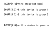
- FIG. 4 is a diagram showing an example of the correspondence between the value of the group setting data and the group to be set.
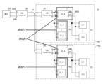
- FIG. 5 is a diagram showing an example of grouping of semiconductor devices.
- FIG. 6 is a diagram showing the data structure of receive data RX when writing is performed with the semiconductor device as the target device.
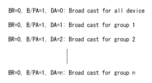
- FIG. 7 is a diagram showing an example of the correspondence between the value of a device address and the group designation for performing broadcasting.
- FIG. 1 is a diagram illustrating a configuration of a communication system according to an exemplary embodiment of the present disclosure.
- FIG. 2 is a block diagram of a semiconductor device according to an exemplary embodiment of the present disclosure.
- FIG. 3 is
- FIG. 8 is a flow diagram showing an example of each step for performing a broadcast.
- FIG. 9 is a diagram showing the data structure of received data RX when a device is accessed using the bridge function.
- FIG. 10 is a timing chart showing communication control when performing a write to a device.
- FIG. 11 is a timing chart showing communication control when performing a read from a device.
- Communication System 1 is a diagram showing a configuration of a communication system 70 according to an exemplary embodiment of the present disclosure.
- the communication system 70 includes an MCU (Micro Controller Unit) 20, a CAN (Controller Area Network) transceiver 30, a CAN transceiver 40, a semiconductor device 1, N devices 10 (N is an integer equal to or greater than 1), a plurality of semiconductor devices 50, and a plurality of semiconductor devices 60.
- the communication system 70 is, as an example, for use in a vehicle.
- the CAN transceiver 40, the semiconductor device 1, the device 10, and the semiconductor device 50 are mounted on the first board PB1.
- the CAN transceiver 40, the semiconductor device 1, the device 10, and the semiconductor device 60 are mounted on the second board PB2.
- UART Universal Asynchronous Receiver/Transmitter
- CAN is a serial communication protocol standardized in international standards such as ISO 11898.
- the CAN transceiver 30 has a TXD (transmit data input) terminal 30A and a RXD (receive data output) terminal 30B.
- the CAN transceiver 30 outputs data input to the TXD terminal 30A to the CAN bus 35, and outputs data input from the CAN bus 35 from the RXD terminal 30B.
- the CAN transceiver 40 and the semiconductor devices 1 and 50 are connected by a bus BS1.
- the bus BS1 is used for communication by UART.
- the CAN transceiver 40 has an RXD terminal 40A and a TXD terminal 40B.
- the CAN transceiver 40 outputs data input to the TXD terminal 40B to the CAN bus 35, and outputs data input from the CAN bus 35 from the RXD terminal 40A.
- the semiconductor device 1 is an IC (integrated circuit) in which circuits with specific functions are integrated, and is configured as, for example, an LED (light emitting diode) driver IC.
- the semiconductor device 1 has an RX (received data input) terminal 1A and a TX (transmitted data output) terminal 1B.
- the multiple semiconductor devices 50 are ICs in which circuits with the same or different functions as the semiconductor device 1 are integrated.
- the semiconductor device 50 has an RX terminal 50A and a TX terminal 50B, just like the semiconductor device 1.
- RX terminals 1A and 50A are commonly connected to RXD terminal 40A.
- TX terminals 1B and 50B are commonly connected to TXD terminal 40B.
- Receive data RX and transmit data TX can be communicated via bus BS1.
- Receive data RX and transmit data TX are serial data conforming to UART.
- Receive data RX output from RXD terminal 40A is input to RX terminals 1A and 50A.
- Transmit data TX output from TX terminals 1B and 50B is input to TXD terminal 40B.
- the N devices 10 are ICs in which circuits with specific functions are integrated, and are configured as, for example, matrix switch ICs.
- the semiconductor device 1 has an RXD terminal 1C and a TXD terminal 1D.
- the RX terminal 10A of each of the N devices 10 is commonly connected to the RXD terminal 1C.
- the TX terminal 10B of each of the N devices 10 is commonly connected to the TXD terminal 1D. That is, the RXD terminal 1C and the TXD terminal 1D are connected to the RX terminal 10A and the TX terminal 10B by a bus (local bus) BS2.
- Communication of received data BRX and transmitted data BTX is possible via the bus BS2.
- the received data BRX and transmitted data BTX are serial data.
- Such a bus BS2 is provided for the bridge function described below.
- the bridge function makes it possible to handle cases where the protocols of the semiconductor device 1 and the device 10 are different.
- CAN transceiver 40, semiconductor device 1, device 10, and semiconductor device 60 on the second board PB2 have the same configuration as those on the first board PB1, so detailed description will be omitted.
- Broadcasting in the communication system 70 according to this embodiment will be described below. Broadcasting is performed between the CAN transceiver 40 and the semiconductor devices 1, 5, and 60 by UART communication.
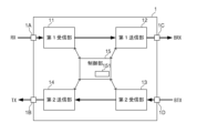
- FIG. 2 is a block diagram of a semiconductor device 1 according to an embodiment of the present disclosure.
- the semiconductor device 1 includes, as functional blocks, a first receiving unit 11, a first transmitting unit 12, a second receiving unit 13, a second transmitting unit 14, and a control unit 15.
- FIG. 2 illustrates only the functional blocks related to the communication function in the communication system 70, and other functional blocks may be included.
- the semiconductor device 1 is an LED driver, it includes a block function related to driving an LED.
- the first receiver 11 receives reception data RX via RX terminal 1A.
- the first transmitter 12 outputs reception data BRX via RXD terminal 1C.
- the second receiver 13 receives transmission data BTX via TXD terminal 1D.
- the second transmitter 14 outputs transmission data TX via TX terminal 1B.
- the control unit 15 controls the first receiving unit 11, the first transmitting unit 12, the second receiving unit 13, and the second transmitting unit 14.
- the control unit 15 has a register 151.
- the semiconductor devices 50 and 60 have the same configuration as that shown in FIG. 2 except for the first transmitting unit 12 and the second receiving unit 13.
- the register map is the correspondence between addresses in a register and stored data.
- semiconductor devices with the same register map are considered to be the same type of semiconductor device, and multiple semiconductor devices 1, 50, and 60 are provided for different types of semiconductor devices 1, 50, and 60.
- FIG. 3 is a register map relating to the grouping function in register 151 of semiconductor device 1.
- register 151 is capable of storing 8 bits of data per address
- group setting data BCGRP is stored at a specific address.
- the group setting data BCGRP is 5-bit data, and is data for setting the group of itself (semiconductor device 1) at the time of broadcasting.
- the group setting data BCGRP is stored in the lowest 5 bits of the 8 bits.
- Semiconductor devices 50 and 60 also have a register map similar to that of FIG. 3, but the specific address is not necessarily the same as that of semiconductor device 1.
- the semiconductor devices 1 are set to group 1 as shown in FIG. 5. In this way, the same type of semiconductor devices 1 mounted on different boards PB1 and PB2 can be set to the same group.
- the multiple semiconductor devices 50 are set to group 2 as shown in FIG. 5.
- the group setting can be made variable by rewriting the group setting data BCGRP via UART communication.
- the group setting is not limited to being variable, and may be fixed. In this case, the groups may be set by, for example, a resistor externally attached to the semiconductor device.
- FIG. 6 shows the data structure of the received data RX when writing to the semiconductor devices 1, 50, and 60 as the target devices.
- a frame FR is made up of bit data from a start bit S to a stop bit P.
- the start bit S is at low level, and the stop bit P is at high level.
- a predetermined number of bits of bit data are placed between the start bit S and the stop bit P.
- 8 bits of bit data are placed.
- a frame FR is made up of 10 bits of bit data.
- the received data RX includes, from the beginning, a synchronization frame SYNC, a read/write etc. frame RWD, a data count frame ND, a register address frame AD, a data frame DT, and a CRC (Cyclic Redundancy Check) frame CR.
- a synchronization frame SYNC a read/write etc. frame RWD
- a data count frame ND a data count frame ND
- a register address frame AD a data frame DT
- CRC Cyclic Redundancy Check
- the synchronization frame SYNC is bit data for setting the baud rate in the semiconductor device.
- the Read/Write etc. frame RWD includes a device address DA, a bridge bit BR, a broadcast/parity bit B/PA, and a Read/Write bit RW.
- the device address DA is bit data indicating the address of the target device (semiconductor device) (5-bit data in the example of Figure 6).
- the bridge bit BR is bit data indicating the on/off state of the bridge function of the semiconductor device 1.
- the broadcast/parity bit B/PA is bit data indicating the on/off state of the broadcast of the semiconductor device 1 or the parity of the data address DA.
- the read/write bit RW is bit data indicating Read or Write.
- broadcast/parity bit B/PA indicates whether broadcast is on or off.
- broadcast/parity bit B/PA 1, it indicates that broadcast is on.
- the broadcast/parity bit B/PA becomes the parity of the device address DA. This makes it possible to detect errors in the device address DA.
- the protocols differ for each group of devices 10 connected to each of the multiple semiconductor devices 1, turning on the broadcast of the semiconductor device 1 will result in the same receive data RX being sent as receive data BRX to devices 10 with different protocols, resulting in protocol incompatibility in some devices 10. For this reason, when the bridge function is turned on, broadcasting is not performed.
- the data number frame ND is bit data indicating the number of frames in the data frame DT.
- the register address frame AD is bit data indicating an address in a register (151, etc.).
- the data frame DT is bit data for writing to a register. Note that the data frame DT is not included in the received data RX when reading.
- the CRC frame CR is bit data indicating an error detection code added to the data frame DT.
- the CAN transceiver 40 transmits the received data RX to the semiconductor devices 1, 50, and 60.
- the control unit (control unit 15, etc.) in the semiconductor device 1, 50, and 60 judges whether the group represented by the device address DA matches the group set in its own semiconductor device. If they match, it is determined that its own semiconductor device is the target of the broadcast, and it is judged whether it is a write or a read based on the Read/Write bit RW included in the received data RX. If it is a write, writing is performed to the register based on the data frame DT included in the received data RX. If it is a read, reading is performed from the register.
- the semiconductor devices can be grouped and broadcast can be performed.
- the semiconductor device 1 and the N devices 10 support different protocols.
- the receive data RX output from the RXD terminal 40A to the RX terminal 1A includes data corresponding to the protocol of the device 10.
- the semiconductor device 1 turns on a bridge function and through-outputs the data included in the receive data RX and corresponding to the protocol of the device 10 as receive data BRX from the RXD terminal 1C.
- Through-output means that bit data is output as is.
- the device address of the device 10 is specified in the receive data BRX.
- device 10 which is the target device (the device specified by the device address) outputs transmission data BTX from TX terminal 10B to TXD terminal 1D. Because the bridge function of semiconductor device 1 is on, the transmission data BTX is output through from TX terminal 1B as transmission data TX.
- the CAN transceiver 40 can write and read to the device 10.
- FIG. 9 is a diagram showing the data structure of the received data RX when performing a write or read operation on device 10 as the target device.
- the synchronization frame SYN and the read/write frame RWD in the received data RX shown in FIG. 9 are as described above.
- the data number frame ND indicates the number of frames for the end condition of the through output, unlike the case shown in FIG. 6. Control using the data number frame ND will be described later.
- the data number frame ND is followed by device data DDT.
- the device data DDT is data that corresponds to the protocol of the device 10, and is the target to be through-output as received data BRX.
- the device data DDT includes a device address BDA.
- the device address BDA indicates the address of the device 10, which is the target device.
- the device address BDA is placed in the device data DDT at a position that corresponds to the protocol of the device 10.
- FIG. 10 is a timing chart showing communication control when performing a write to device 10. From the top of FIG. 10, receive data RX, receive data output selection signal (RX output select), transmit data output selection signal (TX output select), receive data BRX, transmit data BTX, and transmit data TX are shown (similar to FIG. 11).
- receive data RX has the configuration shown in FIG. 9.
- the received data RX is received by the first receiving unit 11 ( Figure 2).
- the control unit 15 By receiving the start bit S1 (low level) at the beginning of the received data RX, the control unit 15 recognizes the start of reception of the received data RX. After that, the control unit 15 recognizes that the bridge function is on from the bridge bit BR included in the received data RX, and recognizes that it is Write from the Read/Write bit RW.
- the control unit 15 changes the received data output selection signal in the register 151 from low to high at the stop bit P1 of the data number frame ND (timing t1). This starts the through output of the received data RX, and the first receiving unit 11 and the first transmitting unit 12 output the received data RX as it is as received data BRX. In other words, the device data DDT ( Figure 9) is output through.
- the control unit 15 When the received data output selection signal goes to high level, the control unit 15 starts counting the number of frames of received data RX (i.e., the number of frames of device data DDT). When the counted number of frames reaches the number of frames indicated by the received data number frames ND, the control unit 15 switches the received data output selection signal to low level and stops the through output (timing t2). After that, the received data BRX is fixed at high level.
- FIG. 11 is a timing chart showing communication control when performing a read on device 10.
- the received data RX has the structure shown in FIG. 9.
- the control unit 15 After receiving the start bit S1 (low level) at the beginning of the received data RX, the control unit 15 recognizes that the bridge function is on based on the bridge bit BR included in the received data RX, and recognizes that it is in a read mode based on the read/write bit RW.
- the control unit 15 changes both the received data output selection signal and the transmitted data output selection signal in the register 151 from low to high at the stop bit P1 of the data number frame ND (timing t1). This starts the through output of the received data RX and transmitted data BTX.
- the first receiving unit 11 and the first transmitting unit 12 output the received data RX as it is as received data BRX, that is, the device data DDT ( Figure 9) is through output.
- the second receiving unit 13 and the second transmitting unit 14 through output the transmitted data BTX sent from the device 10 as transmitted data TX.
- the control unit 15 When the received data output selection signal and the transmitted data output selection signal go to high level, the control unit 15 starts counting the total number of frames of the received received data RX and the received transmitted data BTX. When the counted number of frames reaches the number of frames indicated by the received data number frames ND, the control unit 15 switches both the received data output selection signal and the transmitted data output selection signal to low level, stopping the through output (timing t2). After this, the received data BRX is fixed to high level, and the transmitted data TX is fixed to Hi-z (high impedance).
- the semiconductor device (1) is A semiconductor device comprising: a receiving unit (11) configured to receive communication data (RX) from an external device through serial communication; and a control unit (15), A group of semiconductor devices can be set for the semiconductor device,
- the communication data is First data (B/PA) indicating whether or not the data is broadcast; second data (DA) representing a group of semiconductor devices;
- the control unit is configured to determine that the broadcast is directed to the semiconductor device itself if the group set in the semiconductor device itself matches the group indicated by the second data (first configuration).
- This configuration allows semiconductor devices of the same type to be grouped together for broadcasting, solving the problem of enabling effective broadcasting using serial communication.
- the second data (DA) may be configured to indicate the device address of the target semiconductor device when the first data (B/PA) indicates that the access is a normal access other than the broadcast (second configuration).
- the second data (DA) may be configured to set the communication data to be a broadcast to all semiconductor devices that receive the communication data (third configuration).
- a semiconductor device having any one of the first to third configurations can be connected to an external transmitting device (40) by a first bus (BS1) and can be connected to an external device (10) by a second bus (BS2), a first receiving unit (11) configured to be able to receive the communication data from the transmitting device via the first bus; A first transmission unit (12) configured to be connectable to the device via the second bus; Equipped with The first receiving unit and the first transmitting unit may be configured to, when bridge selection data (BR) included in the communication data indicates that a through output is on, which outputs bit data directly between the first bus and the second bus, output data (DDT) corresponding to the protocol of the device included in the communication data to the second bus (fourth configuration).
- BR bridge selection data
- DDT output data
- the first data indicates whether or not the through output is broadcast;
- the first data may represent a parity bit (fifth configuration).
- the first data (B/PA) and the second data (DA) may be included in the same frame (RWD) of the communication data together with bit data (RW) indicating Read or Write (sixth configuration).
- a register (151) is further provided,
- the group may be set by setting data (BCGRP) stored in the register (seventh configuration).
- a communication system (70) includes a transmitting device (40) configured to transmit the communication data; Any one of the first to seventh semiconductor devices (1, 50, 60) described above, The semiconductor devices having the same register map are regarded as the same type of semiconductor device, and a plurality of the semiconductor devices are provided for each of the different types of semiconductor devices (1, 50, 60) (eighth configuration).
- the semiconductor device (1) of the same type may be arranged separately on multiple substrates (PB1, PB2) (ninth configuration).
- This disclosure can be used, for example, in vehicle-mounted communication systems.
Landscapes
- Engineering & Computer Science (AREA)
- Theoretical Computer Science (AREA)
- Physics & Mathematics (AREA)
- General Engineering & Computer Science (AREA)
- General Physics & Mathematics (AREA)
- Small-Scale Networks (AREA)
Priority Applications (2)
| Application Number | Priority Date | Filing Date | Title |
|---|---|---|---|
| JP2025531454A JPWO2025009346A1 (https=) | 2023-07-06 | 2024-06-12 | |
| CN202480044371.1A CN121444081A (zh) | 2023-07-06 | 2024-06-12 | 半导体装置以及通信系统 |
Applications Claiming Priority (2)
| Application Number | Priority Date | Filing Date | Title |
|---|---|---|---|
| JP2023111351 | 2023-07-06 | ||
| JP2023-111351 | 2023-07-06 |
Publications (1)
| Publication Number | Publication Date |
|---|---|
| WO2025009346A1 true WO2025009346A1 (ja) | 2025-01-09 |
Family
ID=94171651
Family Applications (1)
| Application Number | Title | Priority Date | Filing Date |
|---|---|---|---|
| PCT/JP2024/021377 Pending WO2025009346A1 (ja) | 2023-07-06 | 2024-06-12 | 半導体装置、および通信システム |
Country Status (3)
| Country | Link |
|---|---|
| JP (1) | JPWO2025009346A1 (https=) |
| CN (1) | CN121444081A (https=) |
| WO (1) | WO2025009346A1 (https=) |
Citations (2)
| Publication number | Priority date | Publication date | Assignee | Title |
|---|---|---|---|---|
| JP2000286872A (ja) * | 1999-03-30 | 2000-10-13 | Kawasaki Steel Corp | シリアルデータ転送装置 |
| JP2001067107A (ja) * | 1999-08-30 | 2001-03-16 | Mitsubishi Electric Corp | プログラマブルコントローラシステムおよびその情報伝送制御方法 |
-
2024
- 2024-06-12 JP JP2025531454A patent/JPWO2025009346A1/ja active Pending
- 2024-06-12 WO PCT/JP2024/021377 patent/WO2025009346A1/ja active Pending
- 2024-06-12 CN CN202480044371.1A patent/CN121444081A/zh active Pending
Patent Citations (2)
| Publication number | Priority date | Publication date | Assignee | Title |
|---|---|---|---|---|
| JP2000286872A (ja) * | 1999-03-30 | 2000-10-13 | Kawasaki Steel Corp | シリアルデータ転送装置 |
| JP2001067107A (ja) * | 1999-08-30 | 2001-03-16 | Mitsubishi Electric Corp | プログラマブルコントローラシステムおよびその情報伝送制御方法 |
Also Published As
| Publication number | Publication date |
|---|---|
| CN121444081A (zh) | 2026-01-30 |
| JPWO2025009346A1 (https=) | 2025-01-09 |
Similar Documents
| Publication | Publication Date | Title |
|---|---|---|
| US12120010B2 (en) | Error detection test device for a subscriber station of a serial bus system and method for testing mechanisms for detecting errors in a communication in a serial bus system | |
| US11106618B2 (en) | Method for addressing an integrated circuit on a bus and corresponding device | |
| US10523462B2 (en) | Communication network for transmission of messages | |
| CN100462955C (zh) | 用来与sata装置进行通讯的代用sata主控装置及其相关方法 | |
| US7827335B2 (en) | Remote communication system of a network | |
| JP3757204B2 (ja) | エラー検出/訂正方式及び該方式を用いた制御装置 | |
| US20050144339A1 (en) | Speculative processing of transaction layer packets | |
| CN101304362A (zh) | 重传缓冲装置及传输数据的方法 | |
| WO2025009346A1 (ja) | 半導体装置、および通信システム | |
| WO2002021775A1 (en) | Plural station memory data sharing system | |
| CN118381721B (zh) | 一种在a-phy系统中用i2c广播配置串行器或传感器的方法 | |
| US6732207B2 (en) | Fast serial interface used for controller to robot communications | |
| US20040162956A1 (en) | System and method for implementing a hidden address in a communication module | |
| WO2024009733A1 (ja) | 半導体装置、および通信システム | |
| US11863468B2 (en) | Control of ethernet link-partner GPIO using OAM | |
| EP0569512A4 (en) | Packet transmission system and method utilizing both a data bus and dedicated control lines | |
| JP4970563B2 (ja) | 複数の非ファイバ・チャネル装置をファイバ・チャネル調停ループに結合させるブリッジ装置および方法 | |
| CN101189593A (zh) | 在多路复用的地址/数据总线上进行地址传输期间传送冗余数据的方法 | |
| WO2025009266A1 (ja) | 半導体装置、および通信システム | |
| KR100612454B1 (ko) | I2c 버스 정합 장치 및 방법 | |
| US6460092B1 (en) | Integrated circuit for distributed-type input/output control | |
| US20080091788A1 (en) | Controller, address control method, and data transmission system using the same | |
| US6944176B1 (en) | Method and apparatus for bit level network data multiplexing | |
| JP2026017634A (ja) | 半導体装置、および通信システム | |
| RU2682435C1 (ru) | Интерфейс передачи данных |
Legal Events
| Date | Code | Title | Description |
|---|---|---|---|
| 121 | Ep: the epo has been informed by wipo that ep was designated in this application |
Ref document number: 24835863 Country of ref document: EP Kind code of ref document: A1 |
|
| ENP | Entry into the national phase |
Ref document number: 2025531454 Country of ref document: JP Kind code of ref document: A |
|
| WWE | Wipo information: entry into national phase |
Ref document number: 2025531454 Country of ref document: JP |
|
| NENP | Non-entry into the national phase |
Ref country code: DE |