WO2025009263A1 - 照明装置 - Google Patents
照明装置 Download PDFInfo
- Publication number
- WO2025009263A1 WO2025009263A1 PCT/JP2024/017588 JP2024017588W WO2025009263A1 WO 2025009263 A1 WO2025009263 A1 WO 2025009263A1 JP 2024017588 W JP2024017588 W JP 2024017588W WO 2025009263 A1 WO2025009263 A1 WO 2025009263A1
- Authority
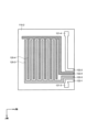
- WO
- WIPO (PCT)
- Prior art keywords
- light
- knob
- liquid crystal
- lighting device
- optical element
- Prior art date
- Legal status (The legal status is an assumption and is not a legal conclusion. Google has not performed a legal analysis and makes no representation as to the accuracy of the status listed.)
- Ceased
Links
Images






Classifications
-
- F—MECHANICAL ENGINEERING; LIGHTING; HEATING; WEAPONS; BLASTING
- F21—LIGHTING
- F21V—FUNCTIONAL FEATURES OR DETAILS OF LIGHTING DEVICES OR SYSTEMS THEREOF; STRUCTURAL COMBINATIONS OF LIGHTING DEVICES WITH OTHER ARTICLES, NOT OTHERWISE PROVIDED FOR
- F21V14/00—Controlling the distribution of the light emitted by adjustment of elements
- F21V14/003—Controlling the distribution of the light emitted by adjustment of elements by interposition of elements with electrically controlled variable light transmissivity, e.g. liquid crystal elements or electrochromic devices
-
- F—MECHANICAL ENGINEERING; LIGHTING; HEATING; WEAPONS; BLASTING
- F21—LIGHTING
- F21L—LIGHTING DEVICES OR SYSTEMS THEREOF, BEING PORTABLE OR SPECIALLY ADAPTED FOR TRANSPORTATION
- F21L4/00—Electric lighting devices with self-contained electric batteries or cells
-
- F—MECHANICAL ENGINEERING; LIGHTING; HEATING; WEAPONS; BLASTING
- F21—LIGHTING
- F21L—LIGHTING DEVICES OR SYSTEMS THEREOF, BEING PORTABLE OR SPECIALLY ADAPTED FOR TRANSPORTATION
- F21L4/00—Electric lighting devices with self-contained electric batteries or cells
- F21L4/005—Electric lighting devices with self-contained electric batteries or cells the device being a pocket lamp
-
- F—MECHANICAL ENGINEERING; LIGHTING; HEATING; WEAPONS; BLASTING
- F21—LIGHTING
- F21V—FUNCTIONAL FEATURES OR DETAILS OF LIGHTING DEVICES OR SYSTEMS THEREOF; STRUCTURAL COMBINATIONS OF LIGHTING DEVICES WITH OTHER ARTICLES, NOT OTHERWISE PROVIDED FOR
- F21V23/00—Arrangement of electric circuit elements in or on lighting devices
- F21V23/04—Arrangement of electric circuit elements in or on lighting devices the elements being switches
-
- F—MECHANICAL ENGINEERING; LIGHTING; HEATING; WEAPONS; BLASTING
- F21—LIGHTING
- F21V—FUNCTIONAL FEATURES OR DETAILS OF LIGHTING DEVICES OR SYSTEMS THEREOF; STRUCTURAL COMBINATIONS OF LIGHTING DEVICES WITH OTHER ARTICLES, NOT OTHERWISE PROVIDED FOR
- F21V9/00—Elements for modifying spectral properties, polarisation or intensity of the light emitted, e.g. filters
- F21V9/40—Elements for modifying spectral properties, polarisation or intensity of the light emitted, e.g. filters with provision for controlling spectral properties, e.g. colour, or intensity
-
- G—PHYSICS
- G02—OPTICS
- G02F—OPTICAL DEVICES OR ARRANGEMENTS FOR THE CONTROL OF LIGHT BY MODIFICATION OF THE OPTICAL PROPERTIES OF THE MEDIA OF THE ELEMENTS INVOLVED THEREIN; NON-LINEAR OPTICS; FREQUENCY-CHANGING OF LIGHT; OPTICAL LOGIC ELEMENTS; OPTICAL ANALOGUE/DIGITAL CONVERTERS
- G02F1/00—Devices or arrangements for the control of the intensity, colour, phase, polarisation or direction of light arriving from an independent light source, e.g. switching, gating or modulating; Non-linear optics
- G02F1/01—Devices or arrangements for the control of the intensity, colour, phase, polarisation or direction of light arriving from an independent light source, e.g. switching, gating or modulating; Non-linear optics for the control of the intensity, phase, polarisation or colour
- G02F1/13—Devices or arrangements for the control of the intensity, colour, phase, polarisation or direction of light arriving from an independent light source, e.g. switching, gating or modulating; Non-linear optics for the control of the intensity, phase, polarisation or colour based on liquid crystals, e.g. single liquid crystal display cells
-
- G—PHYSICS
- G02—OPTICS
- G02F—OPTICAL DEVICES OR ARRANGEMENTS FOR THE CONTROL OF LIGHT BY MODIFICATION OF THE OPTICAL PROPERTIES OF THE MEDIA OF THE ELEMENTS INVOLVED THEREIN; NON-LINEAR OPTICS; FREQUENCY-CHANGING OF LIGHT; OPTICAL LOGIC ELEMENTS; OPTICAL ANALOGUE/DIGITAL CONVERTERS
- G02F1/00—Devices or arrangements for the control of the intensity, colour, phase, polarisation or direction of light arriving from an independent light source, e.g. switching, gating or modulating; Non-linear optics
- G02F1/01—Devices or arrangements for the control of the intensity, colour, phase, polarisation or direction of light arriving from an independent light source, e.g. switching, gating or modulating; Non-linear optics for the control of the intensity, phase, polarisation or colour
- G02F1/13—Devices or arrangements for the control of the intensity, colour, phase, polarisation or direction of light arriving from an independent light source, e.g. switching, gating or modulating; Non-linear optics for the control of the intensity, phase, polarisation or colour based on liquid crystals, e.g. single liquid crystal display cells
- G02F1/133—Constructional arrangements; Operation of liquid crystal cells; Circuit arrangements
- G02F1/1333—Constructional arrangements; Manufacturing methods
-
- G—PHYSICS
- G02—OPTICS
- G02F—OPTICAL DEVICES OR ARRANGEMENTS FOR THE CONTROL OF LIGHT BY MODIFICATION OF THE OPTICAL PROPERTIES OF THE MEDIA OF THE ELEMENTS INVOLVED THEREIN; NON-LINEAR OPTICS; FREQUENCY-CHANGING OF LIGHT; OPTICAL LOGIC ELEMENTS; OPTICAL ANALOGUE/DIGITAL CONVERTERS
- G02F1/00—Devices or arrangements for the control of the intensity, colour, phase, polarisation or direction of light arriving from an independent light source, e.g. switching, gating or modulating; Non-linear optics
- G02F1/01—Devices or arrangements for the control of the intensity, colour, phase, polarisation or direction of light arriving from an independent light source, e.g. switching, gating or modulating; Non-linear optics for the control of the intensity, phase, polarisation or colour
- G02F1/13—Devices or arrangements for the control of the intensity, colour, phase, polarisation or direction of light arriving from an independent light source, e.g. switching, gating or modulating; Non-linear optics for the control of the intensity, phase, polarisation or colour based on liquid crystals, e.g. single liquid crystal display cells
- G02F1/133—Constructional arrangements; Operation of liquid crystal cells; Circuit arrangements
- G02F1/1333—Constructional arrangements; Manufacturing methods
- G02F1/1343—Electrodes
-
- G—PHYSICS
- G02—OPTICS
- G02F—OPTICAL DEVICES OR ARRANGEMENTS FOR THE CONTROL OF LIGHT BY MODIFICATION OF THE OPTICAL PROPERTIES OF THE MEDIA OF THE ELEMENTS INVOLVED THEREIN; NON-LINEAR OPTICS; FREQUENCY-CHANGING OF LIGHT; OPTICAL LOGIC ELEMENTS; OPTICAL ANALOGUE/DIGITAL CONVERTERS
- G02F1/00—Devices or arrangements for the control of the intensity, colour, phase, polarisation or direction of light arriving from an independent light source, e.g. switching, gating or modulating; Non-linear optics
- G02F1/01—Devices or arrangements for the control of the intensity, colour, phase, polarisation or direction of light arriving from an independent light source, e.g. switching, gating or modulating; Non-linear optics for the control of the intensity, phase, polarisation or colour
- G02F1/13—Devices or arrangements for the control of the intensity, colour, phase, polarisation or direction of light arriving from an independent light source, e.g. switching, gating or modulating; Non-linear optics for the control of the intensity, phase, polarisation or colour based on liquid crystals, e.g. single liquid crystal display cells
- G02F1/133—Constructional arrangements; Operation of liquid crystal cells; Circuit arrangements
- G02F1/1333—Constructional arrangements; Manufacturing methods
- G02F1/1347—Arrangement of liquid crystal layers or cells in which the final condition of one light beam is achieved by the addition of the effects of two or more layers or cells
-
- H—ELECTRICITY
- H05—ELECTRIC TECHNIQUES NOT OTHERWISE PROVIDED FOR
- H05B—ELECTRIC HEATING; ELECTRIC LIGHT SOURCES NOT OTHERWISE PROVIDED FOR; CIRCUIT ARRANGEMENTS FOR ELECTRIC LIGHT SOURCES, IN GENERAL
- H05B45/00—Circuit arrangements for operating light-emitting diodes [LED]
- H05B45/10—Controlling the intensity of the light
-
- H—ELECTRICITY
- H05—ELECTRIC TECHNIQUES NOT OTHERWISE PROVIDED FOR
- H05B—ELECTRIC HEATING; ELECTRIC LIGHT SOURCES NOT OTHERWISE PROVIDED FOR; CIRCUIT ARRANGEMENTS FOR ELECTRIC LIGHT SOURCES, IN GENERAL
- H05B47/00—Circuit arrangements for operating light sources in general, i.e. where the type of light source is not relevant
- H05B47/10—Controlling the light source
- H05B47/105—Controlling the light source in response to determined parameters
-
- F—MECHANICAL ENGINEERING; LIGHTING; HEATING; WEAPONS; BLASTING
- F21—LIGHTING
- F21Y—INDEXING SCHEME ASSOCIATED WITH SUBCLASSES F21K, F21L, F21S and F21V, RELATING TO THE FORM OR THE KIND OF THE LIGHT SOURCES OR OF THE COLOUR OF THE LIGHT EMITTED
- F21Y2115/00—Light-generating elements of semiconductor light sources
- F21Y2115/10—Light-emitting diodes [LED]
Definitions
- One embodiment of the present invention relates to a lighting device that uses liquid crystal to control light distribution.
- Portable lighting devices can not only irradiate light in a specific direction, but also have the ability to change the distribution of the irradiated light, thereby increasing the added value of the product.
- Patent Document 1 discloses a flashlight that can distribute light by using a reflector to change the focal length of the light bulb, which is the light source of the flashlight.
- Patent Document 1 by rotating the bezel engaged with the head cover, the reflector disposed within the head cover moves relative to the light bulb.
- the bezel that engages with the head cover on which the optical components including the flashlight reflector are disposed
- the distribution of light emitted from the flashlight changes.
- the user needs to hold the flashlight with one hand while operating the bezel with the other hand.
- such an operation is not necessarily simple and reduces operability for the user.
- liquid crystal lens which utilizes the fact that the refractive index of liquid crystal changes when the voltage applied to the liquid crystal is adjusted.
- a lighting device that uses a liquid crystal lens it is possible to change the light distribution of the lighting device without changing the focal length of the light source.
- One of the objectives of one embodiment of the present invention is to provide a lighting device that is easy for the user to operate and allows the light distribution to be easily adjusted.
- the lighting device includes a light source that emits light, an optical element that includes a liquid crystal cell and transmits the light emitted from the light source in a diffusible manner, a main body that incorporates the light source and the optical element and emits light that transmits through the optical element, and a first slide switch that includes a first knob that is slidably operated relative to the main body and adjusts the distribution angle of the light emitted from the main body by sliding the first knob.
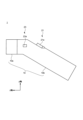
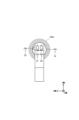
- 1 is a schematic side view showing an external configuration of an illumination device according to an embodiment of the present invention.
- 1 is a schematic top view showing an external configuration of an illumination device according to an embodiment of the present invention;
- 1A and 1B are schematic diagrams illustrating the operation and light distribution of a lighting device according to an embodiment of the present invention.
- 1A and 1B are schematic diagrams illustrating the operation and light distribution of a lighting device according to an embodiment of the present invention.
- 1A and 1B are schematic diagrams illustrating the operation and light distribution of a lighting device according to an embodiment of the present invention.
- 1A and 1B are schematic diagrams illustrating the operation and light distribution of a lighting device according to an embodiment of the present invention.
- 1 is a schematic block diagram showing an internal configuration of a lighting device according to an embodiment of the present invention
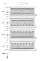
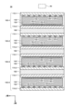
- 1 is a schematic cross-sectional view showing a configuration of an optical element of an illumination device according to one embodiment of the present invention.
- 1 is a schematic cross-sectional view showing a configuration of an optical element of an illumination device according to one embodiment of the present invention.
- 2 is a schematic plan view showing an electrode pattern of a liquid crystal cell included in an optical element of an illumination device according to one embodiment of the present invention.
- FIG. 2 is a schematic plan view showing an electrode pattern of a liquid crystal cell included in an optical element of an illumination device according to one embodiment of the present invention.
- FIG. 1 is a schematic block diagram showing an internal configuration of a lighting device according to an embodiment of the present invention
- 1 is a schematic cross-sectional view showing a configuration of an optical element of an illumination device according to one embodiment of the present invention.
- 2 is a schematic plan view showing an electrode pattern of a liquid crystal cell included in an optical element of an illumination
- 5A and 5B are schematic diagrams illustrating optical characteristics of a liquid crystal cell included in an optical element of an illumination device according to one embodiment of the present invention.
- 5A and 5B are schematic diagrams illustrating optical characteristics of a liquid crystal cell included in an optical element of an illumination device according to one embodiment of the present invention.
- 4 is a schematic diagram showing a signal input to an optical element of an illumination device according to one embodiment of the present invention.
- FIG. 1 is a schematic side view showing an external configuration of an illumination device according to an embodiment of the present invention.
- drawings may show the width, thickness, shape, etc. of each part in a schematic manner compared to the actual embodiment, but these are merely examples, and the illustrated shapes themselves do not limit the interpretation of the present invention.
- components with the same functions as those explained in relation to previous drawings in the specification may be given the same reference numerals even in separate drawings, and duplicate explanations may be omitted.
- each structure When a film is processed to form multiple structures, each structure may have a different function or role, and each structure may be formed on a different base.
- these multiple structures originate from a film formed as the same layer in the same process, and are made of the same material. Therefore, these multiple films are defined as existing in the same layer.
- External configuration of lighting device 1] 1A and 1B are schematic side and top views, respectively, illustrating the external configuration of an illumination device 1 according to one embodiment of the present invention.
- the exterior of the lighting device 1 is composed of a main body 10.
- the main body 10 includes an illumination unit 10a that emits light, and a handle unit 10b that is connected to the illumination unit 10a and is held by a user.
- the lighting device 1 can be used as a flashlight. That is, while holding the handle unit 10b, the user can illuminate the surroundings of the user with light emitted from the illumination unit 10a. Note that the usage of the lighting device 1 is not limited to a flashlight.
- the lighting device 1 can also be used as a spotlight.
- the optical axis direction of the light emitted from the illumination unit 10a is the z-axis direction.
- the light irradiation direction is the +z-axis direction
- the description will simply refer to the z-axis direction.
- the x-axis and y-axis directions are perpendicular to the z-axis direction, and the x-axis and y-axis directions are perpendicular to each other.
- the handle portion 10b extends at a predetermined angle from the z-axis direction.
- the handle axis direction corresponding to the direction in which the handle portion 10b extends is different from the optical axis direction.
- the material that constitutes the main body 10 may be a resin material or a metal material.
- the lighting device 1 includes a first slide switch 21 that adjusts the light distribution angle of the light irradiated from the lighting unit 10a, a second slide switch 22 that adjusts the brightness of the light irradiated from the lighting unit 10a, and a changeover switch 23 that switches the light distribution shape of the light irradiated from the lighting unit 10a.
- the first slide switch 21 includes a first knob 21a that is operated by the user.
- the second slide switch 22 includes a second knob 22a that is operated by the user.
- the changeover switch 23 includes a push button 23a that is operated by the user.
- the first knob 21a of the first slide switch 21 and the second knob 22a of the second slide switch 22 are each provided on the upper surface of the handle portion 10b on the side where the handle portion 10b is connected to the lighting unit 10a.
- the first knob 21a and the second knob 22a are arranged along a direction intersecting the handle axis direction.
- the upper surface of the handle portion 10b is provided with a first guide groove 10c and a second guide groove 10d extending along the handle axis direction.
- the first knob 21a and the second knob 22a are slidably fitted into the first guide groove 10c and the second guide groove 10d, respectively.
- first knob 21a is operated to be slidable in the handle axis direction along the first guide groove 10c
- the second knob 22a is operated to be slidable in the handle axis direction along the second guide groove 10d. Because the first slide switch 21 and the second slide switch 22 have such a configuration, for example, the user can operate both the first knob 21a and the second knob 22a with only the thumb of the hand holding the handle 10b.
- the push button 23a of the changeover switch 23 is provided on the side of the handle portion 10b.
- the changeover switch 23 is a so-called push switch.
- the changeover switch 23 may be a momentary type that maintains the on state only while the push button 23a is pressed, or an alternate type that maintains the on state even after the push button 23a is pressed and then released.
- the changeover switch 23 is not limited to a push switch.
- the changeover switch 23 may be a toggle switch, a rocker switch, a slide switch, or the like.
- the positions of the first knob 21a of the first slide switch 21, the second knob 22a of the second slide switch 22, and the push button 23a of the changeover switch 23 are not limited to the configuration described above.
- the first knob 21a and the second knob 22a may be located on the side of the handle portion 10b, and the push button 23a may be located on the top surface of the handle portion 10b.
- a switch for turning the power of the lighting device 1 on or off may be provided.
- a configuration in which the power of the lighting device 1 can be turned on or off by a changeover switch 23 may also be applied.
- FIGS. 2A to 2D are schematic diagrams showing the operation and light distribution of a lighting device 1 according to one embodiment of the present invention.
- the first knob 21a of the first slide switch 21 and the second knob 22a of the second slide switch 22 are each located in the area farthest from the lighting unit 10a within the slidable range.
- the light 1000 emitted from the lighting unit 10a has a circular light distribution shape.
- the light 1000 emitted from the lighting unit 10a gradually spreads in the x-axis direction and the y-axis direction. In other words, the light distribution angle of the light 1000 emitted from the lighting unit 10a increases. In this way, the light distribution angle of the light 1000 emitted from the lighting unit 10a can be continuously adjusted by sliding the first knob 21a of the first slide switch 21.
- the second slide switch 22 is used to adjust the brightness of the light 1000.
- the brightness of the light 1000 emitted from the illumination unit 10a gradually increases. In this way, the brightness of the light 1000 emitted from the illumination unit 10a can be continuously adjusted by sliding the second knob 22a of the second slide switch 22.
- the second knob 22a of the second slide switch 22 when the second knob 22a of the second slide switch 22 is located in the area farthest from the lighting unit 10a within the slidable range, the brightness of the light 1000 is minimum, and when it is located in the area closest to the lighting unit 10a within the slidable range, the brightness of the light 1000 is maximum.
- the sliding operation of the second knob 22a in adjusting the brightness of the light 1000 may be reversed from the above-mentioned configuration.
- the first slide switch 21 can be used to adjust the light distribution angle of the light 1000 emitted from the lighting unit 10a.
- the second slide switch 22 can be used to adjust the brightness of the light 1000 emitted from the lighting unit 10a.
- the user can slide the first knob 21a of the first slide switch 21 and the second knob 22a of the second slide switch 22 with the fingers (e.g., thumb) of the hand holding the handle 10b while holding the handle 10b. Therefore, the user can adjust the light distribution angle and brightness of the light 1000 emitted from the lighting unit 10a with a simple operation using one hand.
- the user since the light distribution angle and brightness of the light 1000 change continuously, the user can fine-tune the light distribution angle and brightness of the light 1000.
- the lighting device 1 can control the light distribution by not only adjusting the light distribution angle but also by switching the light distribution shape.
- the first knob 21a of the first slide switch 21 is slid, and then the push button 23a of the changeover switch 23 is pressed.
- the light 1000 emitted from the illumination unit 10a has a linear light distribution shape extending in the x-axis direction. In this way, by operating the push button 23a of the changeover switch 23, the light distribution shape of the light 1000 emitted from the illumination unit 10a can be switched.
- the light 1000 irradiated from the illumination unit 10a may have an elliptical or cross-shaped light distribution shape.
- FIG. 3 is a schematic block diagram showing an internal configuration of the lighting device 1 according to an embodiment of the present invention.
- the main body 10 of the lighting device 1 includes an optical element 30, a light source 40, an optical adjustment unit 50, an optical element driving circuit unit 60, a light source driving circuit unit 70, a battery 80, and a charging module 90.
- the optical element 30, the light source 40, and the optical adjustment unit 50 are disposed in the lighting unit 10a of the main body 10.
- the battery 80 and the charging module 90 are disposed in the handle unit 10b of the main body 10.
- the optical element driving circuit unit 60 and the light source driving circuit unit 70 are disposed in the handle unit 10b, but the optical element driving circuit unit 60 and the light source driving circuit unit 70 may be disposed in the lighting unit 10a.
- light emitted from the light source 40 passes through the optical element 30 and is irradiated from the lighting section 10a.
- the optical element driving circuit unit 60 is electrically connected to the battery 80 and is also electrically connected to the optical element 30 via the changeover switch 23.
- the optical element driving circuit unit 60 receives power from the battery 80 and generates a plurality of signals (e.g., pulse signals including rectangular waves) that drive the optical element 30.
- the plurality of signals generated by the optical element driving circuit unit 60 are input to the terminal of the optical element 30 selected by the changeover switch 23.
- the optical element driving circuit unit 60 is also electrically connected to the first slide switch 21.
- the first slide switch 21 is electrically connected to a variable resistor included in the optical element driving circuit unit 60, and when the first knob 21a of the first slide switch 21 is slid, the resistance of the variable resistor changes continuously. This allows the amplitude of the potential included in the plurality of signals to be changed continuously.
- the light source drive circuit section 70 is electrically connected to the light source 40 and the battery 80.
- the light source drive circuit section 70 receives power from the battery 80 and generates a signal to drive the light source 40.
- the light source drive circuit section 70 is also electrically connected to the second slide switch 22.
- the second slide switch 22 is electrically connected to a variable resistor included in the light source drive circuit section, and when the second knob 22a of the second slide switch 22 is slid, the resistance of the variable resistor changes continuously. This makes it possible to continuously change the amount of current included in the signal.
- the battery 80 is electrically connected to the charging module 90.
- the battery 80 can be a so-called secondary battery (e.g., lithium ion battery, etc.) that can be used repeatedly by charging.
- the battery 80 can be charged via the charging module 90.
- the charging module 90 controls the charging of the battery 80 while preventing overcharging of the battery 80.
- the battery 80 can be charged in a wired or wireless configuration. In a wired configuration, the charging module 90 is provided with a terminal for connecting a power cable, and power is charged to the battery 80 via a power cable connected to the terminal of the charging module 90. In a wireless configuration, a power receiving coil is provided in the charging module 90, and the power converted by the power receiving coil is charged to the battery 80.
- a configuration in which the charging module 90 is not provided can also be applied to the lighting device 1.
- a so-called primary battery e.g., alkaline dry battery or manganese dry battery, etc.
- the battery 80 can be used as the battery 80.
- the light source 40 emits light to the optical element 30.
- a light emitting diode LED
- a plurality of LEDs may be used as the light source 40.
- LEDs of the same color may be used, or LEDs of different colors may be used.
- the light source 40 is not limited to an LED.
- the light source 40 may be any element or device that can emit light.
- the optical adjustment unit 50 is disposed between the optical element 30 and the light source 40, and converges, diffuses, or reflects the light emitted from the light source 40.
- the optical adjustment unit 50 is an optical component that is a lens or a reflector, or a combination of these.
- the optical element 30 controls the light distribution (light distribution angle and light distribution shape) of the light emitted from the illumination unit 10a.
- the configuration of the optical element 30 will be described with reference to Figs. 4A to 6B.
- FIG. 4A and 4B are schematic cross-sectional views showing a configuration of an optical element 30 of an illumination device 1 according to an embodiment of the present invention.
- Fig. 4A is a cross-sectional view of the optical element 30 cut along a plane perpendicular to the y-axis direction
- Fig. 4B is a cross-sectional view of the optical element 30 cut along a plane perpendicular to the x-axis direction.
- the optical element 30 includes four liquid crystal cells 100 (first liquid crystal cell 100-1, second liquid crystal cell 100-2, third liquid crystal cell 100-3, and fourth liquid crystal cell 100-4).
- the first liquid crystal cell 100-1, second liquid crystal cell 100-2, third liquid crystal cell 100-3, and fourth liquid crystal cell 100-4 are stacked in order in the z-axis direction from the side closest to the light source 40.
- Light emitted from the light source 40 is incident on the first liquid crystal cell 100-1 and is emitted from the fourth liquid crystal cell 100-4.
- the diffusion and polarization of light are controlled by the four liquid crystal cells 100 included in the optical element 30, and the light distribution of the light emitted from the fourth liquid crystal cell 100-4 can be changed. That is, the optical element 30 transmits the light emitted from the light source 40 in a diffusible manner and can control the light distribution.
- Figures 4A and 4B show the configuration of an optical element 30 including four liquid crystal cells 100
- the number of liquid crystal cells 100 included in the optical element 30 is not limited to four.
- the optical element 30 only needs to include at least one liquid crystal cell 100. However, when emitting light having various light distribution shapes, it is preferable that the optical element 30 includes at least two liquid crystal cells 100.
- each of the first liquid crystal cell 100-1 to the fourth liquid crystal cell 100-4 includes a first substrate 110-1, a second substrate 110-2, a plurality of first transparent electrodes 120-1, a plurality of second transparent electrodes 120-2, a plurality of third transparent electrodes 120-3, a plurality of fourth transparent electrodes 120-4, a first alignment film 130-1, a second alignment film 130-2, a sealant 140, and a liquid crystal layer 150.
- the first transparent electrodes 120-1 and the second transparent electrodes 120-2 are alternately provided on the first substrate 110-1.
- a first alignment film 130-1 is provided on the first substrate 110-1 so as to cover the first transparent electrodes 120-1 and the second transparent electrodes 120-2.
- a third transparent electrode 120-3 and a fourth transparent electrode 120-4 are alternately provided on the second substrate 110-2.
- a second alignment film 130-2 is provided so as to cover the third transparent electrode 120-3 and the fourth transparent electrode 120-4.
- the first substrate 110-1 and the second substrate 110-2 are disposed so that the first transparent electrode 120-1 and the second transparent electrode 120-2 face the third transparent electrode 120-3 and the fourth transparent electrode 120-4, and are bonded via a sealant 140 provided on the periphery of the first substrate 110-1 and the second substrate 110-2.
- a liquid crystal is sealed in the space surrounded by the first substrate 110-1 (more specifically, the first alignment film 130-1), the second substrate 110-2 (more specifically, the second alignment film 130-2), and the sealant 140, and a liquid crystal layer 150 is provided between the first substrate 110-1 and the second substrate 110-2.
- An optically elastic resin layer 160 is provided between the first liquid crystal cell 100-1 and the second liquid crystal cell 100-2. Similarly, an optically elastic resin layer 160 is provided between the second liquid crystal cell 100-2 and the third liquid crystal cell 100-3, and between the third liquid crystal cell 100-3 and the fourth liquid crystal cell 100-4.
- an adhesive containing a light-transmitting acrylic resin can be used as the optically elastic resin layer 160. In other words, the optically elastic resin layer 160 can bond and fix two adjacent liquid crystal cells 100 together.
- Each of the first substrate 110-1 and the second substrate 110-2 may be a rigid substrate having optical transparency, such as a glass substrate, a quartz substrate, or a sapphire substrate. Also, each of the first substrate 110-1 and the second substrate 110-2 may be a flexible substrate having optical transparency, such as a polyimide resin substrate, an acrylic resin substrate, a siloxane resin substrate, or a fluororesin substrate.
- Each of the first transparent electrode 120-1, the second transparent electrode 120-2, the third transparent electrode 120-3, and the fourth transparent electrode 120-4 functions as an electrode for forming an electric field in the liquid crystal layer 150.
- Each of the first transparent electrode 120-1, the second transparent electrode 120-2, the third transparent electrode 120-3, and the fourth transparent electrode 120-4 is made of a transparent conductive material such as indium tin oxide (ITO) or indium zinc oxide (IZO).
- the first transparent electrode 120-1 and the second transparent electrode 120-2 extend in the x-axis direction
- the third transparent electrode 120-3 and the fourth transparent electrode 120-4 extend in the y-axis direction
- the first transparent electrode 120-1 and the second transparent electrode 120-2 extend in the y-axis direction
- the third transparent electrode 120-3 and the fourth transparent electrode 120-4 extend in the x-axis direction.
- the first alignment film 130-1 and the second alignment film 130-2 each align the liquid crystal molecules in the liquid crystal layer 150 in a predetermined direction.
- a polyimide resin or the like is used as each of the first alignment film 130-1 and the second alignment film 130-2.
- each of the first alignment film 130-1 and the second alignment film 130-2 may be given alignment characteristics by an alignment treatment such as a rubbing method or a photo-alignment method.
- the rubbing method is a method in which the surface of the alignment film is rubbed in one direction.
- the photo-alignment method is a method in which the alignment film is irradiated with linearly polarized ultraviolet light.
- the long axes of the liquid crystal molecules on the first substrate 110-1 side are oriented in the y-axis direction, and the long axes of the liquid crystal molecules on the second substrate 110-2 side are oriented in the x-axis direction.
- the long axes of the liquid crystal molecules on the first substrate 110-1 side are aligned in the x-axis direction, and the long axes of the liquid crystal molecules on the second substrate 110-2 side are aligned in the y-axis direction.
- FIG. 5A and 5B are schematic plan views showing the electrode patterns of the liquid crystal cell 100 included in the optical element 30 of the illumination device 1 according to one embodiment of the present invention. Specifically, Fig. 5A is a plan view showing the electrode patterns formed on the first substrate 110-1 of the first liquid crystal cell 100-1, and Fig. 5B is a plan view showing the electrode patterns formed on the second substrate 110-2 of the first liquid crystal cell 100-1.
- a first connection pad 121-1 and a second connection pad 121-2 are provided on a first substrate 110-1.
- a plurality of first transparent electrodes 120-1 are electrically connected to the first connection pad 121-1.
- a plurality of second transparent electrodes 120-2 are electrically connected to the second connection pad 121-2.
- the second substrate 110-2 is provided with a third connection pad 121-3, a fourth connection pad 121-4, a first terminal 122-1, a second terminal 122-2, a third terminal 122-3, and a fourth terminal 122-4.
- the third transparent electrodes 120-3 are electrically connected to the third terminal 122-3.
- the fourth transparent electrodes 120-4 are electrically connected to the fourth terminal 122-4.
- the third connection pad 121-3 is electrically connected to the first terminal 122-1.
- the fourth connection pad 121-4 is electrically connected to the second terminal 122-2.
- the first connection pad 121-1 and the second connection pad 121-2 overlap with the third connection pad 121-3 and the fourth connection pad 121-4, respectively.
- a conductive electrode is provided between the first connection pad 121-1 and the third connection pad 121-3, and the first connection pad 121-1 and the third connection pad 121-3 are electrically connected via the conductive electrode.
- a conductive electrode is provided between the second connection pad 121-2 and the fourth connection pad 121-4, and the second connection pad 121-2 and the fourth connection pad 121-4 are electrically connected via the conductive electrode. Therefore, the first transparent electrode 120-1 and the second transparent electrode 120-2 on the first substrate 110-1 are electrically connected to the first terminal 122-1 and the second terminal 122-2, respectively.
- the electrode pattern of the second liquid crystal cell 100-2 is the same as the electrode pattern of the first liquid crystal cell 100-1.
- the configuration of the electrode patterns of the third liquid crystal cell 100-3 and the fourth liquid crystal cell 100-4 is similar to the configuration of the electrode pattern of the first liquid crystal cell 100-1, except that the extension direction of the transparent electrode 120 differs by 90°.
- the first terminal 122-1 to the fourth terminal 122-4 on the second substrate 110-2 are exposed from the first substrate 110-1.
- the exposed first terminal 122-1 to the fourth terminal 122-4 are electrically connected to the optical element driving circuit unit 60.
- a signal generated by the optical element driving circuit unit 60 is input to the first terminal 122-1 to the fourth terminal 122-4 of each of the first liquid crystal cell 100-1 to the fourth liquid crystal cell 100-4, and a predetermined potential is applied to each of the first transparent electrode 120-1 to the fourth transparent electrode 120-4 of each of the first liquid crystal cell 100-1 to the fourth liquid crystal cell 100-4. This changes the alignment state of the liquid crystal molecules in the liquid crystal layer 150 of each of the first liquid crystal cell 100-1 to the fourth liquid crystal cell 100-4, and can change the distribution of light passing through the optical element 30.
- FIG. 6A and 6B are schematic diagrams illustrating optical characteristics of the liquid crystal cell 100 included in the optical element 30 of the lighting device 1 according to one embodiment of the present invention. Specifically, Fig. 6A shows the liquid crystal cell 100 in a state where no voltage is applied to the transparent electrode 120, and Fig. 6B shows the liquid crystal cell 100 in a state where a voltage is applied to the transparent electrode 120.
- the liquid crystal molecules on the first substrate 110-1 side of the liquid crystal layer 150 are aligned in the y-axis direction, and the liquid crystal molecules on the second substrate 110-2 side of the liquid crystal layer 150 are aligned in the x-axis direction. Therefore, when no voltage is applied to any of the first transparent electrode 120-1 to the fourth transparent electrode 120-4, the liquid crystal molecules in the liquid crystal layer 150 are aligned so as to be twisted 90° as they move from the first substrate 110-1 to the second substrate 110-2. Furthermore, the polarization plane (the direction of the polarization axis or polarization component) of the light passing through the liquid crystal layer 150 is rotated 90° according to the orientation direction of the liquid crystal molecules. In other words, the light passing through the liquid crystal layer 150 (more specifically, the polarization component of the light passing through the liquid crystal layer 150) is rotated.
- the cell gap d which is the distance between the first substrate 110-1 and the second substrate 110-2, is sufficiently larger than the distance between the two adjacent transparent electrodes 120 (for example, 8 ⁇ m ⁇ d ⁇ 50 ⁇ m, preferably 10 ⁇ m ⁇ d ⁇ 30 ⁇ m, and more preferably 15 ⁇ m ⁇ d ⁇ 25 ⁇ m), so the electric field formed between the transparent electrodes 120 does not have much effect on the liquid crystal molecules located near the center between the first substrate 110-1 and the second substrate 110-2.
- the light emitted from the light source 40 contains a polarized component in the x-axis direction (hereinafter referred to as the "P polarized component”) and a polarized component in the y-axis direction (hereinafter referred to as the "S polarized component").
- P polarized component a polarized component in the x-axis direction
- S polarized component a polarized component in the y-axis direction
- the light entering the liquid crystal cell 100 will be described below as being divided into a first light 1000-1 having a P polarized component and a second light 1000-2 having an S polarized component.
- the P-polarized component of the first light 1000-1 incident on the liquid crystal layer 150 from the first substrate 110-1 is different from the orientation direction of the liquid crystal molecules on the first substrate 110-1 side, so the first light 1000-1 is not diffused (see (1) in FIG. 6B).
- the first light 1000-1 is rotated while passing through the liquid crystal layer 150, and the polarization component changes from the P-polarized component to the S-polarized component.
- the S-polarized component of the first light 1000-1 is different from the orientation direction of the liquid crystal molecules on the second substrate 110-2 side, so the first light 1000-1 is not diffused (see (2) in FIG. 6B).
- the P-polarized component of the second light 1000-2 is aligned in the same direction as the liquid crystal molecules on the second substrate 110-2 side, so the second light 1000-2 is diffused in the x-axis direction according to the refractive index distribution of the liquid crystal molecules (see (4) in FIG. 6B).
- [3-4. Input of Signal to Liquid Crystal Cell 100] 7 is a schematic diagram showing signals input to the optical element 30 of the illumination device 1 according to one embodiment of the present invention. In FIG. 7, signals input to the first liquid crystal cell 100-1 of the optical element 30 and electrical connections are shown.
- the seventh shows the first signal S1 to the fifth signal S5 input to the first liquid crystal cell 100-1 of the optical element 30.
- the first signal S1 to the fifth signal S5 are generated by the optical element driving circuit unit 60.
- the first signal S1 and the third signal S3 have a first pulse wave PW1.
- the second signal S2 and the fourth signal S4 have a second pulse wave PW2.
- the first pulse wave PW1 and the second pulse wave PW2 are inverted in phase.
- the fifth signal S5 has a fixed potential P fix .
- the magnitude of the amplitude of the first pulse wave PW1 and the second pulse wave PW2, as well as the magnitude of the fixed potential P fix are continuously changed by the sliding operation of the first knob 21a of the first slide switch 21.
- the first signal S1, the second signal S2, and the fifth signal S5 are input to the first terminal 122-1 or the second terminal 122-2 via the changeover switch 23.
- the third signal S3 and the fourth signal S4 are input to the third terminal 122-3 and the fourth terminal 122-4, respectively.
- the first signal S1 and the second signal S2 are input to the input side contacts 23in_1 and 23in_3, respectively. Furthermore, the fifth signal is input to the input side contacts 23in_2 and 23in_4.
- the first signal S1 and the second signal S2 are input to the first terminal 122-1 and the second terminal 122-2, respectively.
- the third signal S3 and the fourth signal S4 are input to the third terminal 122-3 and the fourth terminal 122-4, respectively.
- a transverse electric field is generated between the first transparent electrode 120-1 and the second transparent electrode 120-2, causing a change in the alignment state of the liquid crystal molecules on the first substrate 110-1 side.
- a transverse electric field is generated between the third transparent electrode 120-3 and the fourth transparent electrode 120-4, causing a change in the alignment state of the liquid crystal molecules on the second substrate 110-2 side.
- the light passing through the first liquid crystal cell 100-1 is diffused in the x-axis and y-axis directions. Therefore, the light irradiated from the lighting device 1 has a circular light distribution shape diffused in the x-axis and y-axis directions.
- a fifth signal S5 is input to the first terminal 122-1 and the second terminal 122-2.
- a third signal S3 and a fourth signal S4 are input to the third terminal 122-3 and the fourth terminal 122-4, respectively. Therefore, a fixed potential P fix is applied to the first transparent electrode 120-1 and the second transparent electrode 120-2, a first pulse wave PW1 is applied to the third transparent electrode 120-3, and a second pulse wave PW2 is applied to the fourth transparent electrode 120-4.
- the size of the light distribution shape changes depending on the magnitude of the voltage applied to the first transparent electrode 120-1 to the fourth transparent electrode 120-4.
- the magnitude of the amplitude of the first pulse wave PW1 and the second pulse wave PW2 input to the first transparent electrode 120-1 to the fourth transparent electrode 120-4 changes continuously by sliding the first knob 21a of the first slide switch 21. Therefore, in the lighting device 1, the size of the light distribution shape can be continuously adjusted by sliding the first knob 21a of the first slide switch 21.
- the changeover switch 23 can be used to switch the light distribution shape of the light 1000 emitted from the lighting unit 10a.
- an elliptical or cross-shaped light distribution shape is also possible by changing the combination of the inputs of the first signal S1 to the fifth signal S5 to the optical element 30.
- a lighting device 1A which is a modified example of the lighting device 1 with reference to Fig. 8.
- the modified example of the lighting device 1 is not limited to the lighting device 1A. Note that, in the following, when the configuration of the lighting device 1A is similar to that of the lighting device 1, the description of the configuration of the lighting device 1A may be omitted.
- FIG. 8 is a schematic side view showing the external configuration of a lighting device 1A according to one embodiment of the present invention.
- the lighting unit 10a and the handle unit 10b are connected without bending.
- the handle axis direction of the handle unit 10b is the same as the optical axis direction.
- the user can hold the handle unit 10b and slide the first knob 21a of the first slide switch 21 and the second knob 22a of the second slide switch 22 with the fingers (e.g., thumb) of the hand holding the handle unit 10b.
- the light distribution and brightness of the light 1000 emitted from the lighting unit 10a can be adjusted by a simple operation.
- the light distribution and brightness can be easily adjusted.
- the user can fine-tune the light distribution angle and brightness of the light 1000.
- connection pads 122-1: first terminal, 122-2: second terminal, 122-3: third terminal, 122-4: fourth terminal, 130-1: first alignment film, 130-2: second alignment film, 140: sealing material, 150: liquid crystal layer, 160: optical elastic resin layer, 1000: light, 1000-1: first light, 1000-2: second light
Landscapes
- Physics & Mathematics (AREA)
- Nonlinear Science (AREA)
- Engineering & Computer Science (AREA)
- General Engineering & Computer Science (AREA)
- Chemical & Material Sciences (AREA)
- Crystallography & Structural Chemistry (AREA)
- General Physics & Mathematics (AREA)
- Optics & Photonics (AREA)
- Mathematical Physics (AREA)
- Spectroscopy & Molecular Physics (AREA)
- Liquid Crystal (AREA)
Abstract
照明装置は、光を出射する光源と、液晶セルを含み、光源から出射された光を拡散可能に透過する光学素子と、光源および光学素子を内蔵し、光学素子を透過する光を照射する本体と、本体に対してスライド可能に操作される第1のつまみを含み、第1のつまみのスライド操作により前記本体から照射される光の配光角を調整する第1のスライドスイッチと、を含む。
Description
本発明の一実施形態は、液晶を用いて配光を制御する照明装置に関する。
携帯型の照明装置、いわゆる懐中電灯では、所定の方向に光を照射するだけでなく、照射された光の配光を変化させる機能を有することにより、製品としての付加価値を高めることができる。例えば、特許文献1には、反射板を用いて、懐中電灯の光源である電球の焦点距離を変化させることにより、配光可能な懐中電灯が開示されている。
特許文献1では、ヘッドカバーに係合されたベゼルを回転させることにより、ヘッドカバー内に配置された反射板が電球に対して移動する。換言すると、ユーザが、懐中電灯の反射板を含む光学部材が配置されたヘッドカバーと係合するベゼルを回すと、懐中電灯から照射される光の配光が変化する。しかしながら、特許文献1に開示された懐中電灯の場合、ユーザの一方の手で懐中電灯の把持しながら、他方の手でベゼルを操作する必要がある。しかしながら、このような操作は必ずしも簡便ではなく、ユーザの操作性を低下させるものである。
一方、液晶に印加する電圧を調整し、液晶の屈折率が変化することを利用した光学素子、いわゆる液晶レンズが知られている。液晶レンズを用いた照明装置では、光源の焦点距離を変化させることなく、照明装置の配光を変化させることが可能である。
本発明の一実施形態は、ユーザの操作性が高く、配光を容易に調整することができる照明装置を提供することを目的の一つとする。
本発明の一実施形態に係る照明装置は、光を出射する光源と、液晶セルを含み、光源から出射された光を拡散可能に透過する光学素子と、光源および光学素子を内蔵し、光学素子を透過する光を照射する本体と、本体に対してスライド可能に操作される第1のつまみを含み、第1のつまみのスライド操作により前記本体から照射される光の配光角を調整する第1のスライドスイッチと、を含む。
以下、本発明の各実施形態において、図面等を参照しつつ説明する。但し、本発明は、その技術的思想の要旨を逸脱しない範囲において様々な態様で実施することができ、以下に例示する実施形態の記載内容に限定して解釈されるものではない。
図面は、説明をより明確にするため、実際の態様に比べ、各部の幅、厚さ、形状等について模式的に表される場合があるが、あくまで一例であって、図示の形状そのものが本発明の解釈を限定するものではない。また、図面において、明細書中で既出の図に関して説明したものと同様の機能を備えた構成要素には、別図であっても同一の符号を付して、重複する説明を省略する場合がある。
ある一つの膜を加工して複数の構造体を形成した場合、各々の構造体は異なる機能、役割を有する場合があり、また各々の構造体はそれが形成される下地が異なる場合がある。しかしながらこれら複数の構造体は、同一の工程で同一層として形成された膜に由来するものであり、同一の材料を有する。従って、これら複数の膜は同一層に存在しているものと定義する。
ある構造体の上に他の構造体を配置する態様を表現するにあたり、単に「上」と表記する場合、特に断りの無い限りは、ある構造体に接して、直上に他の構造体を配置する場合と、ある構造体の上方に、さらに別の構造体を介して他の構造体を配置する場合との両方を含むものとする。
図1A~図6を参照して、本発明の一実施形態に係る照明装置1について説明する。
[1.照明装置1の外観構成]
図1Aおよび図1Bは、それぞれ、本発明の一実施形態に係る照明装置1の外観構成を示す模式的な側面図および上面図である。
図1Aおよび図1Bは、それぞれ、本発明の一実施形態に係る照明装置1の外観構成を示す模式的な側面図および上面図である。
図1Aおよび図1Bに示すように、照明装置1の外観は、本体10によって構成されている。本体10は、光を照射する照明部10aと、照明部10aと接続され、ユーザが把持する持ち手部10bと、を含む。照明装置1は、懐中電灯として利用することができる。すなわち、ユーザは、持ち手部10bを把持しながら、照明部10aから照射される光によって、ユーザの周囲を照らすことができる。なお、照明装置1の利用態様は、懐中電灯に限られない。照明装置1は、スポットライトとしても利用することができる。
なお、以下では、説明の便宜上、照明部10aから照射される光の光軸方向がz軸方向であるとして説明する。また、光の照射方向は+z軸方向であるが、+z軸方向と-z軸方向とを特に区別しない場合には、単にz軸方向として説明する。なお、x軸方向およびy軸方向は、z軸方向と直交する方向であり、x軸方向とy軸方向とは、互いに直交している。
側面視において、持ち手部10bは、z軸方向から所定の角度を有して延伸している。換言すると、持ち手部10bが延伸する方向に対応する持ち手軸方向は、光軸方向と異なっている。照明部10aと持ち手部10bとが屈曲するように接続されていると、ユーザが照明装置1をユーザの顔の近くで使用する場合であっても、ユーザは、ユーザの手首に無理な力をかけることなく持ち手部10bを把持し、照明部10aから照射される光でユーザの周囲を照らすことができる。なお、所定の角度は、15°以上45°以下であるが、これに限られない。また、本体10の形状はこれに限られない。本体10は、照明装置1の利用態様に応じた形状とすることができる。
本体10を構成する材料は、樹脂材料であってもよく、金属材料であってもよい。
照明装置1は、照明部10aから照射される光の配光角を調整する第1のスライドスイッチ21、照明部10aから照射される光の輝度を調整する第2のスライドスイッチ22、および照明部10aから照射される光の配光形状を切り替える切替スイッチ23を含む。第1のスライドスイッチ21は、ユーザによって操作される第1のつまみ21aを含む。第2のスライドスイッチ22は、ユーザによって操作される第2のつまみ22aを含む。切替スイッチ23は、ユーザによって操作される押ボタン23aを含む。
第1のスライドスイッチ21の第1のつまみ21aおよび第2のスライドスイッチ22の第2のつまみ22aの各々は、持ち手部10bの上面において、持ち手部10bが照明部10aと接続される側に設けられている。第1のつまみ21aと第2のつまみ22aとは、持ち手軸方向と交差する方向に沿って配置されている。持ち手部10bの上面には、持ち手軸方向に沿って延在する第1のガイド溝10cおよび第2のガイド溝10dが設けられている。第1のつまみ21aおよび第2のつまみ22aは、それぞれ、第1のガイド溝10cおよび第2のガイド溝10dとスライド可能に嵌合している。すなわち、第1のつまみ21aは、第1のガイド溝10cに沿って持ち手軸方向にスライド可能に操作され、第2のつまみ22aは、第2のガイド溝10dに沿って持ち手軸方向にスライド可能に操作される。第1のスライドスイッチ21および第2のスライドスイッチ22がこのような構成を有することにより、例えば、ユーザは、持ち手部10bを把持した手の親指のみで第1のつまみ21aおよび第2のつまみ22aの両方を操作することが可能となる。
切替スイッチ23の押ボタン23aは、持ち手部10bの側面に設けられている。切替スイッチ23は、いわゆるプッシュスイッチである。切替スイッチ23は、押ボタン23aを押している間のみオン状態を維持するモーメンタリ型であってもよく、押ボタン23aを押した後に離してもオン状態を維持するオルタネート型であってもよい。また、切替スイッチ23は、プッシュスイッチに限られない。切替スイッチ23は、トグルスイッチ、ロッカースイッチ、またはスライドスイッチなどであってもよい。
なお、第1のスライドスイッチ21の第1のつまみ21a、第2のスライドスイッチ22の第2のつまみ22a、および切替スイッチ23の押ボタン23aが配置される位置は、上述した構成に限られない。第1のつまみ21aおよび第2のつまみ22aが持ち手部10bの側面に配置され、押ボタン23aが持ち手部10bの上面に配置されてもよい。
また、図示しないが、照明装置1の電源をオンまたはオフするスイッチが設けられてもよい。あるいは、切替スイッチ23によって照明装置1の電源をオンまたはオフすることができる構成も適用することができる。
ここで、図2A~図2Dを参照して、照明装置1の操作による配光の変化について説明する。
図2A~図2Dは、本発明の一実施形態に係る照明装置1の操作および配光を示す模式図である。
図2Aでは、第1のスライドスイッチ21の第1のつまみ21aおよび第2のスライドスイッチ22の第2のつまみ22aのそれぞれが、スライド可能な範囲のうちの照明部10aから最も離れた領域に位置している。この場合、照明部10aから照射される光1000は、円形状の配光形状を有する。
図2Bに示すように、第1のスライドスイッチ21の第1のつまみ21aがスライド操作されると、照明部10aから照射される光1000は、x軸方向およびy軸方向に徐々に広がる。すなわち、照明部10aから照射される光1000の配光角が大きくなる。このように、第1のスライドスイッチ21の第1のつまみ21aのスライド操作により、照明部10aから照射される光1000の配光角を連続的に調整することができる。
照明装置1では、照明部10aから照射される光1000の配光角が大きくなると、光1000の輝度が低下する。そこで、第2のスライドスイッチ22を用いて、光1000の輝度を調整する。
図2Cに示すように、さらに、第2のスライドスイッチ22の第2のつまみ22aがスライド操作されると、照明部10aから照射される光1000の輝度が徐々に大きくなる。このように、第2のスライドスイッチ22の第2のつまみ22aのスライド操作により、照明部10aから照射される光1000の輝度を連続的に調整することができる。
なお、図2A~図2Cでは、第1のスライドスイッチ21の第1のつまみ21aが、スライド可能な範囲のうちの照明部10aから最も離れた領域に位置するときに光1000の配光角が最小となり、スライド可能な範囲のうちの照明部10aに最も近づく領域に位置するときに光1000の配光角が最大となる。しかしながら、光1000の配光角の調整における第1のつまみ21aのスライド操作は、上述した構成と逆であってもよい。また、第2のスライドスイッチ22の第2のつまみ22aが、スライド可能な範囲のうちの照明部10aから最も離れた領域に位置するときに光1000の輝度が最小となり、スライド可能な範囲のうちの照明部10aに最も近づく領域に位置するときに光1000の輝度が最大となる。しかしながら、光1000の輝度の調整における第2のつまみ22aのスライド操作は、上述した構成と逆であってもよい。
以上説明したように、照明装置1では、第1のスライドスイッチ21を用いて、照明部10aから照射される光1000の配光角を調整することができる。また、照明装置1では、第2のスライドスイッチ22を用いて、照明部10aから照射される光1000の輝度を調整することができる。さらに、照明装置1では、ユーザは、持ち手部10bを把持しながら、第1のスライドスイッチ21の第1のつまみ21aおよび第2のスライドスイッチ22の第2のつまみ22aを、持ち手部10bを把持している手の指(例えば、親指)でスライド操作することが可能である。そのため、ユーザは、片手による簡易な操作により、照明部10aから照射される光1000の配光角および輝度を調整することができる。また、光1000の配光角および輝度は連続的に変化するため、ユーザは、光1000の配光角および輝度を微調整することができる。
また、照明装置1では、配光の制御として、配光角の調整だけでなく、配光形状を切り替えることができる。
図2Dでは、第1のスライドスイッチ21の第1のつまみ21aがスライド操作された後、切替スイッチ23の押ボタン23aが押されている。この場合、照明部10aから照射される光1000は、x軸方向に延伸された直線状の配光形状を有する。このように、切替スイッチ23の押ボタン23aの操作により、照明部10aから照射される光1000の配光形状を切り替えることができる。
なお、上述では、円形状または直線状の配光形状について説明したが、切替スイッチ23によって切り替えられる配光形状は、これらの形状に限られない。照明部10aから照射される光1000は、楕円状または十字状の配光形状を有していてもよい。
[2.照明装置1の内部構成]
図3は、本発明の一実施形態に係る照明装置1の内部構成を示す模式的なブロック図である。
図3は、本発明の一実施形態に係る照明装置1の内部構成を示す模式的なブロック図である。
図3に示すように、照明装置1の本体10の内部には、光学素子30、光源40、光学調整部50、光学素子駆動回路部60、光源駆動回路部70、バッテリ80、および充電モジュール90を含む。光学素子30、光源40、および光学調整部50は、本体10の照明部10a内に配置されている。バッテリ80および充電モジュール90は、本体10の持ち手部10b内に配置されている。図3では、光学素子駆動回路部60および光源駆動回路部70は持ち手部10b内に配置されているが、光学素子駆動回路部60および光源駆動回路部70は照明部10a内に配置されていてもよい。
照明装置1では、光源40から出射された光が、光学素子30を透過し、照明部10aから照射される。
光学素子駆動回路部60は、バッテリ80と電気的に接続され、かつ、切替スイッチ23を介して光学素子30と電気的に接続されている。光学素子駆動回路部60は、バッテリ80から電力が供給され、光学素子30を駆動する複数の信号(例えば、矩形波を含むパルス信号など)を生成する。光学素子駆動回路部60によって生成された複数の信号は、切替スイッチ23によって選択された光学素子30の端子に入力される。また、光学素子駆動回路部60は、第1のスライドスイッチ21と電気的に接続されている。具体的には、第1のスライドスイッチ21は、光学素子駆動回路部60に含まれる可変抵抗器と電気的に接続され、第1のスライドスイッチ21の第1のつまみ21aがスライド操作されると、可変抵抗器の抵抗が連続的に変化する。これにより、複数の信号に含まれる電位の振幅を連続的に変化させることができる。
光源駆動回路部70は、光源40およびバッテリ80と電気的に接続されている。光源駆動回路部70は、バッテリ80から電力が供給され、光源40を駆動する信号を生成する。また、光源駆動回路部70は、第2のスライドスイッチ22と電気的に接続されている。具体的には、第2のスライドスイッチ22は、光源駆動回路部に含まれる可変抵抗器と電気的に接続され、第2のスライドスイッチ22の第2のつまみ22aがスライド操作されると、可変抵抗器の抵抗が連続的に変化する。これにより、信号に含まれる電流量を連続的に変化させることができる。
バッテリ80は、充電モジュール90と電気的に接続されている。バッテリ80として、充電することにより繰り返し使用することができる、いわゆる二次電池(例えば、リチウムイオン電池など)を用いることができる。バッテリ80は、充電モジュール90を介して充電することができる。充電モジュール90は、バッテリ80への過充電を防止しながら、バッテリ80の充電を制御する。バッテリ80への充電は、有線を用いる構成であってもよく、無線を用いる構成であってもよい。有線を用いる構成では、充電モジュール90に電源ケーブルを接続する端子が設けられており、充電モジュール90の端子に接続された電源ケーブルを介してバッテリ80に電力が充電される。また、無線を用いる構成では、充電モジュール90に受電用コイルが設けられており、受電用コイルによって変換された電力がバッテリ80に充電される。なお、照明装置1では、充電モジュール90が設けられない構成も適用可能である。この場合、バッテリ80として、充電することができない、いわゆる一次電池(例えば、アルカリ乾電池またはマンガン乾電池など)を用いることができる。
光源40は、光学素子30に光を出射する。光源40として、例えば、発光ダイオード(LED)を用いることができる。光源40として、複数のLEDが用いられてもよい。光源40として複数のLEDが用いられる場合、同じ色のLEDが用いられてよく、異なる色のLEDが用いられてもよい。なお、光源40はLEDに限定されない。光源40は、光を出射することができる素子または装置であればよい。
光学調整部50は、光学素子30と光源40との間に配置され、光源40から出射された光を収束し、拡散し、または反射する。例えば、光学調整部50は、レンズもしくはリフレクタ、またはこれらを組み合わせた光学部材である。
[3.光学素子30の構成]
光学素子30は、照明部10aから照射される光の配光(配光角および配光形状)を制御する。ここで、図4A~図6Bを参照して、光学素子30の構成について説明する。
光学素子30は、照明部10aから照射される光の配光(配光角および配光形状)を制御する。ここで、図4A~図6Bを参照して、光学素子30の構成について説明する。
[3-1.光学素子30の構造]
図4Aおよび図4Bの各々は、本発明の一実施形態に係る照明装置1の光学素子30の構成を示す模式的な断面図である。図4Aは、y軸方向に垂直な面で切断された光学素子30の断面図であり、図4Bは、x軸方向に垂直な面で切断された光学素子30の断面図である。
図4Aおよび図4Bの各々は、本発明の一実施形態に係る照明装置1の光学素子30の構成を示す模式的な断面図である。図4Aは、y軸方向に垂直な面で切断された光学素子30の断面図であり、図4Bは、x軸方向に垂直な面で切断された光学素子30の断面図である。
光学素子30は、4つの液晶セル100(第1の液晶セル100-1、第2の液晶セル100-2、第3の液晶セル100-3、および第4の液晶セル100-4)を含む。光学素子30では、光源40に近い方から、第1の液晶セル100-1、第2の液晶セル100-2、第3の液晶セル100-3、および第4の液晶セル100-4が、z軸方向に順に積層されている。光源40から出射された光は、第1の液晶セル100-1に入射され、第4の液晶セル100-4から出射される。照明装置1では、光学素子30に含まれる4つの液晶セル100により、光の拡散および偏光が制御され、第4の液晶セル100-4から出射される光の配光を変化させることができる。すなわち、光学素子30は、光源40から出射された光を拡散可能に透過し、配光を制御することができる。
図4Aおよび図4Bには、4つの液晶セル100を含む光学素子30の構成が示されているが、光学素子30に含まれる液晶セル100の数は4つに限られない。光学素子30には、少なくとも1つの液晶セル100が含まれていればよい。但し、様々な配光形状を有する光を照射する場合、光学素子30は、少なくとも2つの液晶セル100を含むことが好ましい。
図4Aおよび図4Bに示すように、第1の液晶セル100-1~第4の液晶セル100-4の各々は、第1の基板110-1、第2の基板110-2、複数の第1の透明電極120-1、複数の第2の透明電極120-2、複数の第3の透明電極120-3、複数の第4の透明電極120-4、第1の配向膜130-1、第2の配向膜130-2、シール材140、および液晶層150を含む。第1の基板110-1上には、第1の透明電極120-1と第2の透明電極120-2とが交互に設けられている。また、第1の基板110-1上には、第1の透明電極120-1および第2の透明電極120-2を覆うように、第1の配向膜130-1が設けられている。第2の基板110-2上には、第3の透明電極120-3と第4の透明電極120-4とが交互に設けられている。また、第2の基板110-2上には、第3の透明電極120-3および第4の透明電極120-4を覆うように、第2の配向膜130-2が設けられている。第1の基板110-1と第2の基板110-2とは、第1の透明電極120-1および第2の透明電極120-2と、第3の透明電極120-3および第4の透明電極120-4とが対向するように配置され、第1の基板110-1および第2の基板110-2の周辺部に設けられたシール材140を介して、接着されている。第1の基板110-1(より具体的には、第1の配向膜130-1)、第2の基板110-2(より具体的には、第2の配向膜130-2)、およびシール材140で囲まれた空間には液晶が封入され、第1の基板110-1と第2の基板110-2との間に液晶層150が設けられている。
第1の液晶セル100-1と第2の液晶セル100-2との間には、光学弾性樹脂層160が設けられている。同様に、第2の液晶セル100-2と第3の液晶セル100-3との間、および第3の液晶セル100-3と第4の液晶セル100-4との間にも、光学弾性樹脂層160が設けられている。光学弾性樹脂層160として、例えば、透光性を有するアクリル樹脂を含む接着剤を用いることができる。すなわち、光学弾性樹脂層160は、隣接する2つの液晶セル100を接着し、固定することができる。
第1の基板110-1および第2の基板110-2の各々として、例えば、ガラス基板、石英基板、またはサファイア基板などの透光性を有する剛性基板が用いられる。また、第1の基板110-1および第2の基板110-2の各々として、例えば、ポリイミド樹脂基板、アクリル樹脂基板、シロキサン樹脂基板、またはフッ素樹脂基板などの透光性を有する可撓性基板を用いることもできる。
第1の透明電極120-1、第2の透明電極120-2、第3の透明電極120-3、および第4の透明電極120-4の各々は、液晶層150に電界を形成するための電極として機能する。第1の透明電極120-1、第2の透明電極120-2、第3の透明電極120-3、および第4の透明電極120-4の各々として、例えば、インジウム・スズ酸化物(ITO)またはインジウム・亜鉛酸化物(IZO)などの透明導電材料が用いられる。
第1の液晶セル100-1および第2の液晶セル100-2において、第1の透明電極120-1および第2の透明電極120-2はx軸方向に延在し、第3の透明電極120-3および第4の透明電極120-4はy軸方向に延在している。また、第3の液晶セル100-3および第4の液晶セル100-4において、第1の透明電極120-1および第2の透明電極120-2はy軸方向に延在し、第3の透明電極120-3および第4の透明電極120-4はx軸方向に延在している。
なお、以下では、第1の透明電極120-1~第4の透明電極120-4を特に区別しないときは、透明電極120として説明する場合がある。
第1の配向膜130-1および第2の配向膜130-2の各々は、液晶層150内の液晶分子を所定の方向に配向させる。第1の配向膜130-1および第2の配向膜130-2の各々として、ポリイミド樹脂などが用いられる。なお、第1の配向膜130-1および第2の配向膜130-2の各々は、ラビング法または光配向法などの配向処理によって配向特性が付与されてもよい。ラビング法は、配向膜の表面を一方向に擦る方法である。また、光配向法は、配向膜に直線偏光の紫外線を照射する方法である。
第1の配向膜130-1は、第1の透明電極120-1および第2の透明電極120-2の延在方向と直交する方向に、液晶層150の第1の基板110-1側の液晶分子が整列するように配向処理が行われる。また、第2の配向膜130-2は、第3の透明電極120-3および第4の透明電極120-4の延在方向と直交する方向に、液晶層150の第2の基板110-2側の液晶分子が整列するように配向処理が行われる。そのため、第1の液晶セル100-1および第2の液晶セル100-2において、第1の基板110-1側の液晶分子の長軸はy軸方向に配向し、第2の基板110-2側の液晶分子の長軸はx軸方向に配向する。また、第3の液晶セル100-3および第4の液晶セル100-4において、第1の基板110-1側の液晶分子の長軸はx軸方向に配向し、第2の基板110-2側の液晶分子の長軸はy軸方向に配向する。
シール材140として、エポキシ樹脂またはアクリル樹脂を含む接着材などが用いられる。なお、接着材は、紫外線硬化型であってもよく、熱硬化型であってもよい。
液晶層150は、液晶分子の配向状態に応じて、透過する光を屈折させ、または透過する光の偏光状態を変化させることができる。液晶層150の液晶として、ネマティック液晶などが用いられる。本実施形態で説明する液晶はポジ型であるが、透明電極120に電圧を印加しない状態における液晶分子の配向方向などを変更することによりネガ型を適用する構成も可能である。また、液晶には、液晶分子にねじれを付与するカイラル剤が含まれていることが好ましい。
[3-2.液晶セル100の電極パターン]
図5Aおよび図5Bの各々は、本発明の一実施形態に係る照明装置1の光学素子30に含まれる液晶セル100の電極パターンを示す模式的な平面図である。具体的には、図5Aは、第1の液晶セル100-1の第1の基板110-1上に形成される電極パターンを示す平面図であり、図5Bは、第1の液晶セル100-1の第2の基板110-2上に形成される電極パターンを示す平面図である。
図5Aおよび図5Bの各々は、本発明の一実施形態に係る照明装置1の光学素子30に含まれる液晶セル100の電極パターンを示す模式的な平面図である。具体的には、図5Aは、第1の液晶セル100-1の第1の基板110-1上に形成される電極パターンを示す平面図であり、図5Bは、第1の液晶セル100-1の第2の基板110-2上に形成される電極パターンを示す平面図である。
図5Aに示すように、第1の基板110-1上には、第1の接続パッド121-1および第2の接続パッド121-2が設けられている。複数の第1の透明電極120-1は、第1の接続パッド121-1と電気的に接続されている。複数の第2の透明電極120-2は、第2の接続パッド121-2と電気的に接続されている。
図5Bに示すように、第2の基板110-2上には、第3の接続パッド121-3、第4の接続パッド121-4、第1の端子122-1、第2の端子122-2、第3の端子122-3、および第4の端子122-4が設けられている。複数の第3の透明電極120-3は、第3の端子122-3と電気的に接続されている。複数の第4の透明電極120-4は、第4の端子122-4と電気的に接続されている。また、第3の接続パッド121-3は、第1の端子122-1と電気的に接続されている。第4の接続パッド121-4は、第2の端子122-2と電気的に接続されている。
各透明電極120が対向するように第1の基板110-1と第2の基板110-2とが貼り合わせられると、第1の接続パッド121-1および第2の接続パッド121-2は、それぞれ、第3の接続パッド121-3および第4の接続パッド121-4と重畳する。第1の接続パッド121-1と第3の接続パッド121-3との間には、導通電極が設けられており、第1の接続パッド121-1と第3の接続パッド121-3とは、導通電極を介して電気的に接続されている。同様に、第2の接続パッド121-2と第4の接続パッド121-4との間にも、導通電極が設けられており、第2の接続パッド121-2と第4の接続パッド121-4とは、導通電極を介して電気的に接続されている。したがって、第1の基板110-1上の第1の透明電極120-1および第2の透明電極120-2は、それぞれ、第1の端子122-1および第2の端子122-2と電気的に接続されている。
第2の液晶セル100-2の電極パターンは、第1の液晶セル100-1の電極パターンと同一である。第3の液晶セル100-3および第4の液晶セル100-4の電極パターンの構成は、透明電極120の延在方向が90°異なる点を除き、第1の液晶セル100-1の電極パターンの構成と同様である。
液晶セル100では、第2の基板110-2上の第1の端子122-1~第4の端子122-4が、第1の基板110-1から露出されている。第1の液晶セル100-1~第4の液晶セル100-4の各々において、露出された第1の端子122-1~第4の端子122-4は、光学素子駆動回路部60と電気的に接続されている。詳細は後述するが、光学素子駆動回路部60により生成される信号が第1の液晶セル100-1~第4の液晶セル100-4の各々の第1の端子122-1~第4の端子122-4に入力されることにより、第1の液晶セル100-1~第4の液晶セル100-4の各々の第1の透明電極120-1~第4の透明電極120-4のそれぞれに所定の電位が印加される。これにより、第1の液晶セル100-1~第4の液晶セル100-4の各々の液晶層150の液晶分子の配向状態が変化し、光学素子30を透過する光の配光を変化させることができる。
[3-3.液晶セル100の光学特性]
図6Aおよび図6Bの各々は、本発明の一実施形態に係る照明装置1の光学素子30に含まれる液晶セル100の光学特性を説明する模式図である。具体的には、図6Aは、透明電極120に電圧が印加されていない状態の液晶セル100を示し、図6Bは、透明電極120に電圧が印加されている状態の液晶セル100を示す。
図6Aおよび図6Bの各々は、本発明の一実施形態に係る照明装置1の光学素子30に含まれる液晶セル100の光学特性を説明する模式図である。具体的には、図6Aは、透明電極120に電圧が印加されていない状態の液晶セル100を示し、図6Bは、透明電極120に電圧が印加されている状態の液晶セル100を示す。
図6Aに示すように、液晶層150の第1の基板110-1側の液晶分子はy軸方向に配向し、液晶層150の第2の基板110-2側の液晶分子はx軸方向に配向している。そのため、第1の透明電極120-1~第4の透明電極120-4のいずれにも電圧が印加されていない状態では、液晶層150内の液晶分子は、第1の基板110-1から第2の基板110-2に向かうにつれて90°捩じれるように配向する。また、液晶層150を透過する光は、液晶分子の配向方向に従って、偏光面(偏光軸または偏光成分の向き)が90°回転される。すなわち、液晶層150を透過する光(より具体的には、液晶層150を透過する光の偏光成分)は、旋光する。
一方、隣接する2つの透明電極120間で電位差が生じるように電圧が印加されると、隣接する2つの透明電極120間に電界(以下、「横電界」という。)が発生し、液晶分子の配向状態が変化する。図6Bに示すように、液晶層150内の液晶分子は、第1の基板110-1から第2の基板110-2に向かうにつれて90°捩じれるように配向しながら、第1の基板110-1近傍の液晶分子は、第1の透明電極120-1と第2の透明電極120-2との間の横電界によって第1の基板110-1に対して凸円弧状に配列し、第2の基板110-2近傍の液晶分子は、第3の透明電極120-3と第4の透明電極120-4との間の横電界によって第2の基板110-2に対して凸円弧状に配列する。凸円弧状に配列した液晶分子は屈折率分布を有し、液晶分子の配向方向に沿った光の偏光成分が拡散される。なお、第1の基板110-1と第2の基板110-2の間の間隔であるセルギャップdは、隣接する2つの透明電極120間の距離よりも十分に大きい(例えば、8μm≦d≦50μm、好ましくは10μm≦d≦30μm、さらに好ましくは15μm≦d≦25μm)ため、第1の基板110-1と第2の基板110-2との間の中央近傍に位置する液晶分子には上記透明電極120間に形成される電界はあまり影響しない。
光源40から出射された光は、x軸方向の偏光成分(以下、「P偏光成分」という。)およびy軸方向の偏光成分(以下、「S偏光成分」という。)を含むが、以下では、便宜上、液晶セル100に入射する光を、P偏光成分を有する第1の光1000-1とS偏光成分を有する第2の光1000-2とに分けて説明する。
第1の基板110-1から液晶層150に入射した第1の光1000-1のP偏光成分は、第1の基板110-1側の液晶分子の配向方向と異なるため、第1の光1000-1は拡散されない(図6B中の(1)参照)。また、第1の光1000-1は、液晶層150を通過する過程で旋光し、偏光成分がP偏光成分からS偏光成分に変化する。第1の光1000-1のS偏光成分は、第2の基板110-2側の液晶分子の配向方向と異なるため、第1の光1000-1は拡散されない(図6B中の(2)参照)。
第1の基板110-1から液晶層150に入射した第2の光1000-2のS偏光成分は、第1の基板110-1側の液晶分子の配向方向と同じであるため、第2の光1000-2は、液晶分子の屈折率分布に従ってy軸方向に拡散される(図6B中の(3)参照)。また、第2の光1000-2は、液晶層150を通過する過程で旋光し、偏光成分がS偏光成分からP偏光成分に変化する。第2の光1000-2のP偏光成分は、第2の基板110-2側の液晶分子の配向方向と同じであるため、第2の光1000-2は、液晶分子の屈折率分布に従ってx軸方向に拡散される(図6B中の(4)参照)。
以上の説明は1つの液晶セル100の構成であるが、複数の液晶セル100を含む光学素子30では、複数の液晶セル100のそれぞれによって、光学素子30に入射する光のP偏光成分またはS偏光成分が制御される。
[3-4.液晶セル100への信号の入力]
図7は、本発明の一実施形態に係る照明装置1の光学素子30に入力される信号を示す模式図である。図7には、光学素子30の第1の液晶セル100-1に入力される信号および電気的接続が示されている。
図7は、本発明の一実施形態に係る照明装置1の光学素子30に入力される信号を示す模式図である。図7には、光学素子30の第1の液晶セル100-1に入力される信号および電気的接続が示されている。
図7には、光学素子30の第1の液晶セル100-1に入力される第1の信号S1~第5の信号S5が示されている。第1の信号S1~第5の信号S5は、光学素子駆動回路部60によって生成される。第1の信号S1および第3の信号S3は、第1のパルス波PW1を有する。第2の信号S2および第4の信号S4は、第2のパルス波PW2を有する。第1のパルス波PW1と第2のパルス波PW2とは、位相が反転している。また、第5の信号S5は、固定電位Pfixを有する。なお、第1のパルス波PW1および第2のパルス波PW2の振幅の大きさ、ならびに固定電位Pfixの大きさは、第1のスライドスイッチ21の第1のつまみ21aによるスライド操作によって連続的に変化する。第1の信号S1、第2の信号S2、および第5の信号S5は、切替スイッチ23を介して、第1の端子122-1または第2の端子122-2に入力される。第3の信号S3および第4の信号は、それぞれ、第3の端子122-3および第4の端子122-4に入力される。
切替スイッチ23は、複数の入力側接点23in_1、23in_2、23in_3、23in_4、および複数の出力側接点23out_1、23out_2を含む。切替スイッチ23において、出力側接点23out_1は、入力側接点23in_1、23in_2の1つと電気的に接続され、出力側接点23out_2は、入力側接点23in_3、23in_4の1つと電気的に接続される。切替スイッチ23における出力側接点23out_1、23out_2の電気的接続は連動している。出力側接点23out_1が入力側接点23in_1と電気的に接続されるとき、出力側接点23out_2は入力側接点23in_3と電気的に接続される。一方、出力側接点23out_1が入力側接点23in_2と電気的に接続されるとき、出力側接点23out_2は入力側接点23in_4と電気的に接続される。切替スイッチ23の押ボタン23aが押されるたびに、出力側接点23out_1、23out_2の電気的接続が切り替わる。
図7に示すように、入力側接点23in_1、23in_3には、それぞれ、第1の信号S1および第2の信号S2が入力される。また、入力側接点23in_2、23in_4には、第5の信号が入力される。
出力側接点23out_1、23out_2が、それぞれ、入力側接点23in_1、23in_3と電気的に接続されると、第1の端子122-1および第2の端子122-2には、それぞれ、第1の信号S1および第2の信号S2が入力される。また、第3の端子122-3および第4の端子122-4には、それぞれ、第3の信号S3および第4の信号S4が入力される。
この場合、第1の透明電極120-1と第2の透明電極120-2との間で横電界が発生し、第1の基板110-1側の液晶分子の配向状態が変化する。また、第3の透明電極120-3と第4の透明電極120-4との間で横電界が発生し、第2の基板110-2側の液晶分子の配向状態が変化する。そのため、第1の液晶セル100-1を透過する光は、x軸方向およびy軸方向に拡散される。したがって、照明装置1から照射される光は、x軸方向およびy軸方向に拡散された円形状の配光形状を有する。
出力側接点23out_1、23out_2が、それぞれ、入力側接点23in_2、23in_4と電気的に接続されると、第1の端子122-1および第2の端子122-2には、第5の信号S5が入力される。また、第3の端子122-3および第4の端子122-4には、それぞれ、第3の信号S3および第4の信号S4が入力される。そのため、第1の透明電極120-1および第2の透明電極120-2には固定電位Pfixが印加され、第3の透明電極120-3には第1のパルス波PW1が印加され、および第4の透明電極120-4には第2のパルス波PW2が印加される。
この場合、第1の透明電極120-1と第2の透明電極120-2との間で横電界は発生せず、第1の基板110-1側の液晶分子の配向状態は変化しない。一方、第3の透明電極120-3と第4の透明電極120-4との間で横電界が発生し、第2の基板110-2側の液晶分子の配向状態が変化する。そのため、第1の液晶セル100-1を透過する光は、x軸方向に拡散される。したがって、照明装置1から照射される光は、x軸方向に延伸された直線状の配光形状を有する。
配光形状の大きさは、第1の透明電極120-1~第4の透明電極120-4に印加する電圧の大きさによって変化する。照明装置1では、第1の透明電極120-1~第4の透明電極120-4に入力される第1のパルス波PW1および第2のパルス波PW2の振幅の大きさは、第1のスライドスイッチ21の第1のつまみ21aによるスライド操作によって連続的に変化する。そのため、照明装置1では、第1のスライドスイッチ21の第1のつまみ21aのスライド操作により、配光形状の大きさを連続的に調整することができる。
上述したように、照明装置1では、切替スイッチ23を用いて、照明部10aから照射される光1000の配光形状を切り替えることができる。なお、照明装置1では、光学素子30への第1の信号S1~第5の信号S5の入力の組み合わせを変えることにより、楕円状または十字状の配光形状も可能である。
<変形例>
図8を参照して、照明装置1の一変形例である照明装置1Aについて説明する。なお、照明装置1の変形例は、照明装置1Aに限られない。なお、以下では、照明装置1Aの構成が照明装置1の構成と同様であるとき、照明装置1Aの構成の説明を省略する場合がある。
図8を参照して、照明装置1の一変形例である照明装置1Aについて説明する。なお、照明装置1の変形例は、照明装置1Aに限られない。なお、以下では、照明装置1Aの構成が照明装置1の構成と同様であるとき、照明装置1Aの構成の説明を省略する場合がある。
図8は、本発明の一実施形態に係る照明装置1Aの外観構成を示す模式的な側面図である。
照明装置1Aでは、照明部10aと持ち手部10bとが屈曲することなく接続されている。すなわち、持ち手部10bの持ち手軸方向は、光軸方向と同じである。本体10がこのような形状を有していても、ユーザは、持ち手部10bを把持しながら、第1のスライドスイッチ21の第1のつまみ21aおよび第2のスライドスイッチ22の第2のつまみ22aを、持ち手部10bを把持している手の指(例えば、親指)でスライド操作することが可能である。
以上説明したように、変形例も含め、本実施形態に係る照明装置1では、簡易な操作により、照明部10aから照射される光1000の配光および輝度を調整することができる。換言すると、照明装置1では、配光および輝度を容易に調整することができる。また、光1000の配光角および輝度は連続的に変化するため、ユーザは、光1000の配光角および輝度を微調整することができる。
本発明の思想の範疇において、当業者であれば、各種の変更例および修正例に相当し得るものであり、それら変更例および修正例についても本発明の範囲に属するものと了解される。例えば、上述の各実施形態に対して、当業者が適宜、構成要素の追加、削除もしくは設計変更を行ったもの、または、工程の追加、省略もしくは条件変更を行ったものも、本発明の要旨を備えている限り、本発明の範囲に含まれる。
また、各実施形態によりもたらされる他の作用効果について本明細書の記載から明らかなもの、または当業者において適宜想到し得るものについては、当然に本発明によりもたらされるものと解される。
1、1A:照明装置、 10:本体、 10a:照明部、 10b:持ち手部、 10c:第1のガイド溝、 10d:第2のガイド溝、 21:第1のスライドスイッチ、 21a:第1のつまみ、 22:第2のスライドスイッチ、 22a:第2のつまみ、 23:切替スイッチ、 23a:押ボタン、 23in:入力側接点、 23out:出力側接点、 30:光学素子、 40:光源、 50:光学調整部、 60:光学素子駆動回路部、 70:光源駆動回路部、 80:バッテリ、 90:充電モジュール、 100:液晶セル、 100-1:第1の液晶セル、 100-2:第2の液晶セル、 100-3:第3の液晶セル、 100-4:第4の液晶セル、 110-1:第1の基板、 110-2:第2の基板、 120:透明電極、 120-1:第1の透明電極、 120-2:第2の透明電極、 120-3:第3の透明電極、 120-4:第4の透明電極、 121-1:第1の接続パッド、 121-2:第2の接続パッド、 121-3:第3の接続パッド、 121-4:第4の接続パッド、 122-1:第1の端子、 122-2:第2の端子、 122-3:第3の端子、 122-4:第4の端子、 130-1:第1の配向膜、 130-2:第2の配向膜、 140:シール材、 150:液晶層、 160:光学弾性樹脂層、 1000:光、 1000-1:第1の光、 1000-2:第2の光
Claims (9)
- 光を出射する光源と、
液晶セルを含み、前記光源から出射された前記光を拡散可能に透過する光学素子と、
前記光源および前記光学素子を内蔵し、前記光学素子を透過する前記光を照射する本体と、
前記本体に対してスライド可能に操作される第1のつまみを含み、前記第1のつまみのスライド操作により前記本体から照射される前記光の配光角を調整する第1のスライドスイッチと、を含む、照明装置。 - 前記第1のスライドスイッチは、前記光学素子と接続され、
前記第1のつまみの前記スライド操作により、前記液晶セルに含まれる透明電極に印加する電圧の大きさが連続的に変化する、請求項1に記載の照明装置。 - さらに、前記本体に対してスライド可能に操作される第2のつまみを含み、前記第2のつまみのスライド操作により前記本体から照射される前記光の輝度を調整する第2のスライドスイッチを含む、請求項1に記載の照明装置。
- 前記第2のスライドスイッチは、前記光源と接続され、
前記第2のつまみの前記スライド操作により、前記光源に供給される電流量が連続的に変化する、請求項3に記載の照明装置。 - 前記本体は、
前記光を照射する照明部と、
前記照明部と接続され、前記第1のつまみが設置される持ち手部と、を含み、
前記照明部から照射される前記光の光軸方向は、前記持ち手部が延伸する持ち手軸方向と異なる、請求項1に記載の照明装置。 - 前記本体は、
前記光を照射する照明部と、
前記照明部と接続され、前記第1のつまみが設置される持ち手部と、を含み、
前記照明部から照射される前記光の光軸方向は、前記持ち手部が延伸する持ち手軸方向と同じである、請求項1に記載の照明装置。 - 前記第1のつまみは、前記持ち手軸方向にスライド可能である、請求項5または請求項6に記載の照明装置。
- さらに、前記本体に対してスライド可能に操作される第2のつまみを含み、前記第2のつまみのスライド操作により前記本体から照射される前記光の輝度を調整する第2のスライドスイッチを含み、
前記本体は、
前記光を照射する照明部と、
前記照明部と接続され、前記第1のつまみおよび前記第2のつまみが設置される持ち手部と、を含み、
前記第1のつまみと前記第2のつまみとは、前記持ち手軸方向と交差する方向に沿って配置されている、請求項1に記載の照明装置。 - さらに、前記光学素子と接続され、前記本体から照射される前記光の配光形状を切り替える切替スイッチを含む、請求項1に記載の照明装置。
Priority Applications (2)
| Application Number | Priority Date | Filing Date | Title |
|---|---|---|---|
| JP2025530999A JPWO2025009263A1 (ja) | 2023-07-05 | 2024-05-13 | |
| US19/408,540 US20260085815A1 (en) | 2023-07-05 | 2025-12-04 | Lighting device |
Applications Claiming Priority (2)
| Application Number | Priority Date | Filing Date | Title |
|---|---|---|---|
| JP2023110578 | 2023-07-05 | ||
| JP2023-110578 | 2023-07-05 |
Related Child Applications (1)
| Application Number | Title | Priority Date | Filing Date |
|---|---|---|---|
| US19/408,540 Continuation US20260085815A1 (en) | 2023-07-05 | 2025-12-04 | Lighting device |
Publications (1)
| Publication Number | Publication Date |
|---|---|
| WO2025009263A1 true WO2025009263A1 (ja) | 2025-01-09 |
Family
ID=94171840
Family Applications (1)
| Application Number | Title | Priority Date | Filing Date |
|---|---|---|---|
| PCT/JP2024/017588 Ceased WO2025009263A1 (ja) | 2023-07-05 | 2024-05-13 | 照明装置 |
Country Status (3)
| Country | Link |
|---|---|
| US (1) | US20260085815A1 (ja) |
| JP (1) | JPWO2025009263A1 (ja) |
| WO (1) | WO2025009263A1 (ja) |
Citations (5)
| Publication number | Priority date | Publication date | Assignee | Title |
|---|---|---|---|---|
| JPS62140603U (ja) * | 1986-02-28 | 1987-09-04 | ||
| JPH0659239A (ja) * | 1992-08-07 | 1994-03-04 | Sony Corp | プロジェクタ装置 |
| JP2004253226A (ja) * | 2003-02-19 | 2004-09-09 | Saipaaku:Kk | 光出力装置 |
| JP2009012150A (ja) * | 2007-07-09 | 2009-01-22 | Max Co Ltd | 照明装置およびその照明装置を備える建築用の駆動工具 |
| JP2009180857A (ja) * | 2008-01-30 | 2009-08-13 | Seiko Epson Corp | プロジェクタ及びこれを備える携帯機器 |
-
2024
- 2024-05-13 WO PCT/JP2024/017588 patent/WO2025009263A1/ja not_active Ceased
- 2024-05-13 JP JP2025530999A patent/JPWO2025009263A1/ja active Pending
-
2025
- 2025-12-04 US US19/408,540 patent/US20260085815A1/en active Pending
Patent Citations (5)
| Publication number | Priority date | Publication date | Assignee | Title |
|---|---|---|---|---|
| JPS62140603U (ja) * | 1986-02-28 | 1987-09-04 | ||
| JPH0659239A (ja) * | 1992-08-07 | 1994-03-04 | Sony Corp | プロジェクタ装置 |
| JP2004253226A (ja) * | 2003-02-19 | 2004-09-09 | Saipaaku:Kk | 光出力装置 |
| JP2009012150A (ja) * | 2007-07-09 | 2009-01-22 | Max Co Ltd | 照明装置およびその照明装置を備える建築用の駆動工具 |
| JP2009180857A (ja) * | 2008-01-30 | 2009-08-13 | Seiko Epson Corp | プロジェクタ及びこれを備える携帯機器 |
Also Published As
| Publication number | Publication date |
|---|---|
| JPWO2025009263A1 (ja) | 2025-01-09 |
| US20260085815A1 (en) | 2026-03-26 |
Similar Documents
| Publication | Publication Date | Title |
|---|---|---|
| JP2005317879A (ja) | 液晶レンズ付き発光装置 | |
| TW200613803A (en) | Liquid crystal lens element and optical head device | |
| JP2012069458A (ja) | 車両用灯具 | |
| US20230375159A1 (en) | Optical element and lighting device | |
| JP7649907B2 (ja) | 光学素子 | |
| WO2025009263A1 (ja) | 照明装置 | |
| US20260071735A1 (en) | Lighting device | |
| JP7534544B2 (ja) | 照明装置 | |
| KR20240134155A (ko) | 조명 장치 | |
| JP7496037B2 (ja) | 液晶光学素子及び照明装置 | |
| WO2024176604A1 (ja) | 照明装置 | |
| CN117255966B (zh) | 液晶光学元件及照明装置 | |
| JP7802197B2 (ja) | 光学素子および照明装置 | |
| JP7796893B2 (ja) | 照明装置 | |
| US12554167B2 (en) | Lighting device | |
| JP7733838B2 (ja) | 照明システム | |
| JP2011233433A (ja) | 照明装置 | |
| JP5213261B2 (ja) | 照明装置 | |
| US20250155758A1 (en) | Optical device | |
| WO2025204021A1 (ja) | 光学素子および照明装置 | |
| HK40092885A (zh) | 光学元件和照明装置 | |
| WO2025220296A1 (ja) | 液晶セル、光学素子、および照明装置 | |
| JP2024133921A (ja) | 照明装置 | |
| WO2025062811A1 (ja) | 液晶光学素子及び照明装置 | |
| JP2014022106A (ja) | 照明装置 |
Legal Events
| Date | Code | Title | Description |
|---|---|---|---|
| 121 | Ep: the epo has been informed by wipo that ep was designated in this application |
Ref document number: 24835785 Country of ref document: EP Kind code of ref document: A1 |
|
| ENP | Entry into the national phase |
Ref document number: 2025530999 Country of ref document: JP Kind code of ref document: A |
|
| WWE | Wipo information: entry into national phase |
Ref document number: 2025530999 Country of ref document: JP |
|
| NENP | Non-entry into the national phase |
Ref country code: DE |