WO2025009262A1 - 位相同期回路、撮像装置および電子回路 - Google Patents
位相同期回路、撮像装置および電子回路 Download PDFInfo
- Publication number
- WO2025009262A1 WO2025009262A1 PCT/JP2024/017484 JP2024017484W WO2025009262A1 WO 2025009262 A1 WO2025009262 A1 WO 2025009262A1 JP 2024017484 W JP2024017484 W JP 2024017484W WO 2025009262 A1 WO2025009262 A1 WO 2025009262A1
- Authority
- WO
- WIPO (PCT)
- Prior art keywords
- time
- locked loop
- converter
- voltage
- phase
- Prior art date
- Legal status (The legal status is an assumption and is not a legal conclusion. Google has not performed a legal analysis and makes no representation as to the accuracy of the status listed.)
- Ceased
Links
Images






Classifications
-
- H—ELECTRICITY
- H03—ELECTRONIC CIRCUITRY
- H03K—PULSE TECHNIQUE
- H03K5/00—Manipulating of pulses not covered by one of the other main groups of this subclass
- H03K5/22—Circuits having more than one input and one output for comparing pulses or pulse trains with each other according to input signal characteristics, e.g. slope, integral
- H03K5/26—Circuits having more than one input and one output for comparing pulses or pulse trains with each other according to input signal characteristics, e.g. slope, integral the characteristic being duration, interval, position, frequency, or sequence
-
- H—ELECTRICITY
- H03—ELECTRONIC CIRCUITRY
- H03L—AUTOMATIC CONTROL, STARTING, SYNCHRONISATION OR STABILISATION OF GENERATORS OF ELECTRONIC OSCILLATIONS OR PULSES
- H03L7/00—Automatic control of frequency or phase; Synchronisation
- H03L7/06—Automatic control of frequency or phase; Synchronisation using a reference signal applied to a frequency- or phase-locked loop
- H03L7/08—Details of the phase-locked loop
- H03L7/085—Details of the phase-locked loop concerning mainly the frequency- or phase-detection arrangement including the filtering or amplification of its output signal
- H03L7/091—Details of the phase-locked loop concerning mainly the frequency- or phase-detection arrangement including the filtering or amplification of its output signal the phase or frequency detector using a sampling device
-
- H—ELECTRICITY
- H03—ELECTRONIC CIRCUITRY
- H03L—AUTOMATIC CONTROL, STARTING, SYNCHRONISATION OR STABILISATION OF GENERATORS OF ELECTRONIC OSCILLATIONS OR PULSES
- H03L7/00—Automatic control of frequency or phase; Synchronisation
- H03L7/06—Automatic control of frequency or phase; Synchronisation using a reference signal applied to a frequency- or phase-locked loop
- H03L7/08—Details of the phase-locked loop
- H03L7/099—Details of the phase-locked loop concerning mainly the controlled oscillator of the loop
-
- H—ELECTRICITY
- H03—ELECTRONIC CIRCUITRY
- H03M—CODING; DECODING; CODE CONVERSION IN GENERAL
- H03M1/00—Analogue/digital conversion; Digital/analogue conversion
- H03M1/12—Analogue/digital converters
- H03M1/50—Analogue/digital converters with intermediate conversion to time interval
Definitions
- This technology relates to a phase-locked loop circuit, an imaging device, and an electronic circuit. More specifically, this technology relates to a phase-locked loop circuit, an imaging device, and an electronic circuit that use an ADPLL (All Digital PLL).
- ADPLL All Digital PLL
- a time-to-digital converter detects the phase difference (time difference) between a reference clock and the output signal of a digitally controlled oscillator (DCO) in the time domain.
- DCO digitally controlled oscillator
- a digital PLL circuit has been proposed that includes a sample-and-hold circuit that samples the phase difference between the DCO output signal and the reference signal as a voltage (see, for example, Patent Document 1).
- This technology was developed in light of these circumstances, and aims to reduce jitter while suppressing increases in the circuit size of phase-locked loop circuits.
- the present technology has been made to solve the above-mentioned problems, and its first aspect is a phase-locked loop circuit that includes a sample-and-hold circuit that subsamples an input signal based on a reference signal, a voltage-to-time converter that converts the voltage of the input signal subsampled by the sample-and-hold circuit into a time difference, and a time-to-digital converter that detects the time difference converted by the voltage-to-time converter. This brings about the effect that the time resolution of the input signal is set based on the voltage resolution of the input signal.
- the sample-and-hold circuit, the voltage-to-time converter, and the time-to-digital converter may form a time-domain ADC (Analog to Digital Converter). This provides the effect of setting the time resolution of the input signal based on the AD.
- ADC Analog to Digital Converter
- the time resolution of the time domain ADC may be higher than the time resolution of the time-to-digital converter. This has the effect of reducing jitter caused by limitations in the time resolution of the time-to-digital converter.
- the device may further include a digitally controlled oscillator that generates the input signal. This provides the effect of adjusting the frequency of the input signal based on the control of the digital code input to the digitally controlled oscillator voltage.
- the device may further include an accumulator that sets a count-up value for each period of the reference signal based on a Frequency Command Word (FCW), a counter that counts up for each period of the input signal, an arithmetic unit that subtracts the output of the counter and the output of the time-to-digital converter from the output of the accumulator, and a loop filter that band-limits the input to the digitally controlled oscillator.
- FCW Frequency Command Word
- the device may further include a frequency divider that divides the input signal generated by the digitally controlled oscillator. This provides the effect of inputting the divided input signal to the time domain ADC.
- the device may further include a digital time converter that delays the reference signal. This has the effect of adjusting the decimal phase shift in a fractional PLL (Phase Locked Loop).
- PLL Phase Locked Loop
- the time-to-digital converter may further include a selector that switches between an input of the time difference converted by the voltage-to-time converter and an input of the reference signal and the input signal. This provides the effect of simultaneously expanding the lock range of the phase-locked loop and improving the time resolution.
- the selector may input the time difference converted by the voltage-to-time converter to the time-to-digital converter when the subsampling mode is specified, and input the reference signal and the input signal to the time-to-digital converter when the normal mode is specified. This provides the effect of switching between the subsampling mode and the normal mode.
- the normal mode may be operated intermittently while operating in the subsampling mode. This provides the effect of improving time resolution while stabilizing phase synchronization.
- the phase-locked loop may be calibrated. This has the effect of improving the stability of the phase lock.
- the second aspect is an imaging device that includes an imaging section having a plurality of pixels, and a phase-locked loop circuit that generates a clock signal that sets the operation timing of the imaging section, the phase-locked loop circuit including a sample-and-hold circuit that subsamples the clock signal based on a reference clock, a voltage-to-time converter that converts the voltage of the clock signal subsampled by the sample-and-hold circuit into a time difference, and a time-to-digital converter that detects the time difference converted by the voltage-to-time converter.
- This provides the effect of setting the time resolution of the clock signal based on the voltage resolution of the clock signal used in the imaging device.
- the third aspect is an electronic circuit comprising a circuit section that operates based on a clock signal, and a phase-locked loop circuit that generates a clock signal that sets the operation timing of the circuit section, the phase-locked loop circuit comprising a sample-and-hold circuit that subsamples the clock signal based on a reference clock, a voltage-to-time converter that converts the voltage of the clock signal subsampled by the sample-and-hold circuit into a time difference, and a time-to-digital converter that detects the time difference converted by the voltage-to-time converter.
- This provides the effect that the time resolution of the clock signal is set based on the voltage resolution of the clock signal used in the electronic circuit.
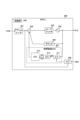
- FIG. 1 is a block diagram showing a configuration example of a phase locked loop according to a first embodiment
- 4 is a timing chart showing waveforms at various points in the phase locked loop according to the first embodiment
- 4 is a timing chart showing a relationship between a clock signal and a reference clock in the phase locked loop circuit according to the first embodiment
- 4 is a diagram illustrating a first example of a relationship between an offset frequency and phase noise of the phase locked loop according to the first embodiment
- 11 is a diagram illustrating a second example of the relationship between the offset frequency and the phase noise of the phase locked loop according to the first embodiment.
- FIG. FIG. 2 illustrates an example of the configuration of a time-to-digital converter according to the first embodiment
- FIG. 2 illustrates an example of the configuration of a digital time converter according to the first embodiment
- FIG. 2 illustrates an example of the configuration of a digital time converter according to the first embodiment
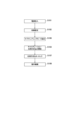
- 4 is a flowchart showing an operation of the phase locked loop circuit according to the first embodiment
- 10 is a flowchart showing an operation of the phase locked loop circuit according to the second embodiment
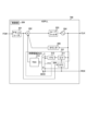
- FIG. 13 is a block diagram showing a configuration example of a phase locked loop circuit according to a third embodiment
- 13 is a flowchart showing an operation of the phase locked loop circuit according to the third embodiment
- FIG. 13 is a block diagram showing a configuration example of a phase locked loop according to a fourth embodiment
- FIG. 13 is a block diagram showing a configuration example of a phase locked loop according to a fifth embodiment
- FIG. 13 is a block diagram showing an example of the configuration of an imaging device to which a phase synchronization circuit according to a sixth embodiment is applied.
- FIG. 13 is a block diagram illustrating an example of the configuration of a solid-state imaging device according to a sixth embodiment.
- FIG. 23 is a perspective view showing an example of a stack of a pixel array unit according to a seventh embodiment; 1 is a block diagram showing a schematic configuration example of a vehicle control system;
- FIG. 4 is an explanatory diagram showing an example of an installation position of an imaging unit.
- First embodiment an example in which the voltage of a clock signal subsampled by a sample-and-hold circuit is converted into a time difference by a voltage-to-time converter, and the time difference is detected by a time-to-digital converter
- Second embodiment example of performing calibration of phase-locked loop after mode setting
- Third embodiment example of operation in subsampling mode only
- Fourth embodiment example in which a reference clock is input to a selector without using a digital time converter
- Fifth embodiment (example of dividing a clock signal output from a digitally controlled oscillator) 6.
- Sixth embodiment (example in which a phase-locked loop is applied to an imaging device) 7.
- Seventh embodiment (example in which pixel array sections are stacked) 8. Examples of applications to moving objects
- FIG. 1 is a block diagram showing an example of the configuration of a phase locked loop according to a first embodiment.
- ADPLL200 is provided as a phase-locked loop circuit.
- ADPLL200 forms a feedback loop based on phase synchronization and outputs a clock signal CLK.
- the frequency of the clock signal CLK can be determined based on a frequency command word (FCW).
- the FCW can specify the ratio of the frequency of the clock signal CLK to the frequency of the reference clock RCK.
- the FCW can include an integer int and a decimal frc.
- the FCW can be provided from outside the ADPLL200.
- the ADPLL200 includes an accumulator 201, a calculator 202, a loop filter 203, a digitally controlled oscillator 204, a counter 206, a time domain ADC 207, a digital time converter 208, and a control unit 209.
- the digitally controlled oscillator 204 generates a clock signal CLK based on an oscillation operation.
- the digitally controlled oscillator 204 can change the oscillation frequency based on an oscillator tuning word.
- the digitally controlled oscillator 204 may be a ring oscillator or an LC oscillator.
- the counter 206 counts up for each clock of the clock signal CLK and outputs the count value to the calculator 202. At this time, the counter 206 can detect the phase in units of one cycle of the clock signal CLK.
- the accumulator 201 sets a count-up value for each period of the reference clock RCK based on the FCW, and outputs it to the calculator 202. At this time, the FCW is input to the accumulator 201. The accumulator 201 can then output the integer int specified by the FCW to the calculator 202, and output the decimal frc specified by the FCW to the digital-to-time converter (DTC) 208.
- DTC digital-to-time converter
- the calculator 202 subtracts the output of the counter 206 and the output of the time-to-digital converter 214 from the output of the accumulator 201, and outputs the result to the loop filter 203.
- the output of the calculator 202 can indicate the phase error between the reference clock RCK and the clock signal CLK.
- the ADPLL 200 can operate the phase-locked loop so that the phase error approaches zero.
- the loop filter 203 band-limits the input to the digitally controlled oscillator 204 to reduce the effects of quantization errors.
- the gain of the loop filter 203 can be adjusted based on the calibration of the ADPLL 200.
- the digital time converter 208 delays the reference clock RCK and outputs it to the sample-and-hold circuit 211 and the selector 213.
- a phase shift occurs by a decimal point each time the clock signal CLK is sub-sampled based on the reference clock RCK. Since the value of this phase shift is known, the digital time converter 208 can set the delay time so that this phase shift is corrected. By correcting the phase shift in the digital time converter 208, it is possible to eliminate the need to expand the range of the time-to-digital converter 214 to accommodate this phase shift.
- the time-to-digital converter 214 only needs to cover a relatively narrow range that includes the resolution of the digital time converter 208, the jitter of the digitally controlled oscillator 204, and a margin to accommodate other errors. Note that the digital time converter 208 is not necessary in the integer PLL.
- the time domain ADC 207 performs AD conversion in the time domain.
- the time resolution of the time domain ADC 207 can be higher than the time resolution of the time digital converter 214.
- the time domain ADC 207 includes a sample and hold circuit 211, a voltage-to-time converter 212, a selector 213, and a time-to-digital converter 214.
- the sample-and-hold circuit 211 subsamples the clock signal CLK based on the reference clock RCK.
- the sample-and-hold circuit 211 then holds the subsampled sample-and-hold value SH and outputs it to a voltage-to-time converter (VTC) 212.
- VTC voltage-to-time converter
- the voltage-to-time converter 212 converts the voltage of the clock signal CLK subsampled by the sample-and-hold circuit 211 into a time difference. At this time, the voltage-to-time converter 212 can set the time difference between the rising edges of the output voltages VP and VN based on the sample-and-hold value SH held in the sample-and-hold circuit 211.
- the selector 213 switches between inputting the time difference converted by the voltage-time converter 212 and inputting the reference clock RCK and clock signal CLK to the time-digital converter 214.
- the selector 213 can switch between the subsampling mode and the normal mode based on the mode setting signal MOD.
- the selector 213 inputs the time difference converted by the voltage-time converter 212 to the time-digital converter 214.
- the selector 213 inputs the reference clock RCK and the clock signal CLK to the time-digital converter 214.
- the time digital converter (TDC) 214 detects the time difference converted by the voltage-time converter 212, digitizes it, and outputs it to the calculator 202.
- the time difference detected by the time digital converter 214 is magnified and input.
- the time digital converter 214 detects the time difference between the reference clock RCK and the clock signal CLK, digitizes it, and outputs it to the calculator 202.
- the time digital converter 214 may be a delay line TDC.
- the time difference detected by the time-to-digital converter 214 is magnified based on the gain from the input of the sample-and-hold circuit 211 to the input of the time-to-digital converter 214.
- the gain from the input of the sample-and-hold circuit 211 to the input of the time-to-digital converter 214 can be given as follows:
- the voltage gain for a time shift ⁇ tck of the clock signal CLK is 2 ⁇ fck Vck ⁇ tck.
- the gain TG of the voltage-time converter 212 is a design value; for example, with an input of 100 mV, 200 psec can be achieved.
- the gain from the time lag ⁇ tck at the input of the sample-and-hold circuit 211 to the time lag ⁇ tvo at the output of the voltage-to-time converter 212 can be given by the following formula.
- the sample-and-hold circuit 211 and the voltage-to-time converter 212 before the time-to-digital converter 214, gain is provided in the time domain, and the time lag near the zero crossing of the clock signal CLK is amplified by 25.1 times before being input to the time-to-digital converter 214.
- the time resolution is converted into an input, if the TDC time resolution is 20 psec, the input-converted time resolution is approximately 0.8 psec, which is an equivalent improvement in time resolution.
- the control unit 209 performs overall control of the ADPLL 200.
- the control unit 209 can control the operation sequence of the ADPLL 200, supply an enable signal when the ADPLL 200 is started, switch the mode of the ADPLL 200, and set the coefficients of the loop filter 203.
- FIG. 2 is a timing chart showing the waveforms of each part of the phase-locked loop circuit according to the first embodiment.
- the sample-and-hold circuit 211 subsamples the clock signal CLK and holds the sample-and-hold value SH.
- the voltage-time converter 212 raises the output voltage VN based on the sample-and-hold value SH held in the sample-and-hold circuit 211 (t2).
- the voltage-time converter 212 raises the output voltage VP after a time difference DT according to the sample-and-hold value SH has elapsed (t3).
- the time difference DT may be proportional to the sample-and-hold value SH.
- FIG. 3 is a timing chart showing the relationship between the clock signal and the reference clock of the phase-locked loop circuit according to the first embodiment. Note that in the figure, a shows an example of operation in normal mode. In the figure, b shows an example of operation in subsampling mode.
- the time-to-digital converter 214 detects the time difference between the reference clock RCK and the clock signal CLK. At this time, a value of 20 psec, for example, can be obtained as the TDC time resolution.
- the voltage-to-time converter 212 converts the voltage VD of the clock signal CLK subsampled by the sample-and-hold circuit 211 into a time difference.
- a value of 0.8 psec can be obtained as the time resolution.
- the gain TG of the voltage-to-time converter 212 is 200 psec/100 mV.
- the voltage VD of the clock signal CLK is converted into a time difference. Therefore, in subsampling, the time difference between the reference clock RCK and the clock signal CLK is affected by the period of the clock signal CLK, narrowing the lock range LR2.
- This lock range LR2 is limited to within ⁇ /4 rad.
- the normal mode may be operated intermittently while operating in the subsampling mode.
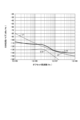
- FIG. 4 is a diagram showing a first example of the relationship between the offset frequency and phase noise of the phase locked loop circuit according to the first embodiment. Note that this diagram shows the relationship between the offset frequency and phase noise in normal mode. Also, L1 indicates the phase noise of the OL-DCO, L2 indicates the phase noise of the TDC, L3 indicates the phase noise of the DCO, and L4 indicates the total phase noise.
- the quantization noise of the time-to-digital converter 214 contributes significantly to the jitter of the ADPLL 200, resulting in a jitter of 1.8 psec.
- FIG. 5 is a diagram showing a second example of the relationship between the offset frequency and phase noise of the phase locked loop circuit according to the first embodiment. Note that this diagram shows the relationship between the offset frequency and phase noise in the subsampling mode.
- the quantization noise of the time-to-digital converter 214 would be approximately 10 dB smaller than the other noises and would no longer be the dominant term.
- the jitter of the ADPLL 200 would be reduced to 0.6 psec.
- Normal mode has a wide and robust lock range LR1, so various calibrations immediately after startup can be performed in normal mode, and then switching to subsampling mode allows for safe startup. Normal mode also has larger jitter than subsampling mode, but is robust and has low power consumption, so an appropriate mode can be selected for each application. Furthermore, by inserting normal mode between subsampling modes, cycle slips during subsampling operation can be prevented, making it possible to both expand the lock range and improve time resolution.
- FIG. 6 is a diagram showing an example of the configuration of a time-to-digital converter according to the first embodiment. Note that in this figure, an example is shown in which the time-to-digital converter 214 is a delay line TDC.
- the time-to-digital converter 214 includes delay buffers 311 to 313 and flip-flops 321 to 323.
- the reference clock RCK is input via buffer 301, delayed by an integer multiple of the buffer delay ⁇ in delay buffers 311 to 313, and input to the D terminals of flip-flops 321 to 323, respectively.
- the clock signal CLK is input to the CK terminal of each of the flip-flops 321 to 323 via the buffer 302.
- each of the flip-flops 321 to 323 captures the state of the reference clock RCK of the delay line at the rising edge of the clock signal CLK. This makes it possible to measure how many stages of buffer delay the time interval until the rising edge of the clock signal CLK corresponds to, and to convert the time into a digital value.
- the buffer delay ⁇ on the path of the reference clock RCK becomes the minimum time resolution.
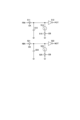
- FIG. 7 is a diagram showing an example of the configuration of a digital time converter according to the first embodiment. Note that in the figure, a shows a first example of the digital time converter 208, b shows a second example of the digital time converter 208, and c shows a third example of the digital time converter 208.
- a first example of the digital time converter 208 includes inverters 401 and 402, capacitors 411 to 413, and field effect transistors 421 to 423.
- the inverters 401 and 402 are connected in series with each other.
- Each of the capacitors 411 to 413 is connected in series with a corresponding one of the field effect transistors 421 to 423.
- the series circuits of each of the capacitors 411 to 413 and each of the field effect transistors 421 to 423 are connected in parallel between the inverters 401 and 402.
- the series circuits of each of the capacitors 411 to 413 and each of the field effect transistors 421 to 423 can be operated as variable capacitances.
- a second example of the digital time converter 208 includes inverters 431 to 433, capacitors 441 to 443, and a selector 403.
- Capacitors 441 to 443 are connected in parallel to the outputs of the inverters 431 to 433, respectively.
- the parallel circuits of the inverters 431 to 433 and the capacitors 441 to 443 can have mutually different delay amounts.
- the selector 403 can select one of the outputs of the inverters 431 to 433.
- a third example of the digital time converter 208 includes wires 451 to 454 and a selector 404.
- Wires 451 to 454 can have different propagation delays.
- Selector 404 can select one of wires 451 to 454.
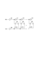
- FIG. 8 shows an example of the configuration of a digital time converter according to the first embodiment.
- the digital time converter 208 includes switches 511, 521, 515, 525, inverters 512, 522, capacitors 513, 523, and current sources 514, 524.
- Switch 511 is connected in series to inverter 512.
- Switch 521 is connected in series to inverter 522.
- Current source 514 is connected in series to switch 515.
- Current source 524 is connected in series to switch 525.
- a series circuit of capacitor 513, current source 514, and switch 515 is connected in parallel between switch 511 and inverter 512.
- a series circuit of capacitor 523, current source 524, and switch 525 is connected in parallel between switch 521 and inverter 522.
- Each switch 511, 521 is turned on/off based on clock CL.
- Each switch 515, 525 is turned on/off based on inverted clock CB.
- Inverted clock CB is a signal obtained by inverting clock CL.
- the inputs PIN and NIN are input through switches 511 and 521, respectively, and the outputs POT and NOT are output through inverters 512 and 522, respectively.
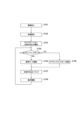
- FIG. 9 is a flowchart showing the operation of the phase locked loop circuit according to the first embodiment.
- calibration and phase locking of ADPLL 200 is started (S103).
- the gain of the normal path and the subsampling path are detected and reflected in the loop filter in order to prevent operational malfunctions and maintain low jitter while keeping the loop gain constant.
- the following methods can be used to detect each gain.
- an error can be detected by using a correlation value between the output of time-to-digital converter 214 and the input to digital-to-time converter 208, and the delay amount (time) for the input code of digital-to-time converter 208 can be calculated.
- the method disclosed in the following document may be used. "Y. -H. Liu et al., "An Ultra-Low Power 1.7-2.7 GHz Fractional-N Sub-Sampling Digital Frequency Synthesizer and Modulator for IoT Applications in 40 nm CMOS," in IEEE Transactions on Circuits and Systems I: Regular Papers, vol. 64, no. 5, pp. 1094-1105, May 2017, doi: 10.1109/TCSI.2016.2625462.”
- the gain of the normal path can be determined by shifting the DTC input code and comparing the amount of shift with the amount of change in the TDC output code to determine the DTC input code for the TDC1 code. Since the relationship between the DTC input code and time is known, the time corresponding to the TDC1 code can be determined.
- the gain of the subsampling path can be calculated by combining the sample-and-hold circuit 211, the voltage-to-time converter 212, and the time-to-digital converter 214 to obtain the time corresponding to the TDC1 code.
- ADPLL200 determines whether or not subsampling mode has been specified (S104). If subsampling mode has not been specified, ADPLL200 continues to operate in normal mode (S105). On the other hand, if subsampling mode has been specified, ADPLL200 sets the subsampling mode (S106).
- the low robustness of the subsampling mode can be compensated for.
- the phase shift can be measured and normal operation can be restored as long as it is within the detection range of the time-to-digital converter 214.
- the phase may shift more than expected because it is not known how much the frequency of the digitally controlled oscillator 204 will move in relation to the adjustment amount.
- appropriate control is possible if the detection range of the time-to-digital converter 214 is designed to be wide. The same effect can be obtained for unexpected disturbances.
- the phase is detected based on the slope of the sine wave, so if the phase deviates by more than ⁇ 90 degrees from the clock signal CLK, the slope will invert and control will be impossible. Therefore, at startup, the device operates in normal mode, and ADPLL 200 performs calibration to ensure safe startup. After that, low-jitter operation is performed in subsampling mode, making it possible to achieve both robustness and low-jitter operation.
- ADPLL 200 performs phase pull-in and locking (S107) and continues operation (S108).
- ADPLL 200 can return to S104 while operation continues and determine whether subsampling mode has been specified.
- the voltage of the clock signal CLK subsampled by the sample-and-hold circuit 211 is converted into a time difference by the voltage-to-time converter 212, and the time difference is detected by the time-to-digital converter TDC.
- the time difference detected by the time-to-digital converter 214 can be enlarged. Therefore, the time resolution of the ADPLL 200 can be improved while complying with the constraints of the TDC time resolution.
- Second embodiment In the first embodiment described above, the calibration of the phase-locked loop is performed before the mode is set, whereas in the second embodiment, the calibration of the phase-locked loop is performed after the mode is set.
- FIG. 10 is a flowchart showing the operation of the phase locked loop circuit according to the second embodiment.
- the calibration and phase locking of the ADPLL 200 starts (S103) after the mode is set (S105, S106).
- the rest of the flow in the second embodiment is the same as the flow in the first embodiment described above.
- by performing the calibration after the mode is set it becomes possible to perform the calibration while the normal mode is continuing, and the calibration can be stabilized.
- the subsampling mode and the normal mode can be switched via the selector 213.
- the selector 213 is removed, and the phase locked loop operates only in the subsampling mode.
- FIG. 11 is a block diagram showing an example of the configuration of a phase-locked loop circuit according to the third embodiment.
- ADPLL 600 includes a time-domain ADC 607 instead of the time-domain ADC 207 of the first embodiment described above.
- the rest of the configuration of ADPLL 600 of the third embodiment is the same as the configuration of ADPLL 200 of the first embodiment described above.
- the time-domain ADC 607 is obtained by removing the selector 213 from the time-domain ADC 207 of the first embodiment described above.
- the clock signal CLK is input to the sample-and-hold circuit 211
- the reference clock RCK is input to the sample-and-hold circuit 211 via the digital-to-time converter 208.
- the output voltages VP and VN of the voltage-to-time converter 212 are input to the time-to-digital converter 214.
- the ADPLL 600 can operate only in the subsampling mode.
- the rest of the configuration of the time-domain ADC 607 of the third embodiment is the same as the configuration of the time-domain ADC 207 of the first embodiment described above.
- FIG. 12 is a flowchart showing the operation of the phase locked loop circuit according to the third embodiment.
- the phase-locked loop circuit operates only in the subsampling mode. This makes it possible to eliminate the need for the selector 213 and the need for mode switching control, thereby simplifying control and reducing the circuit size.
- the reference clock RCK is input to the selector 213 via the digital time converter 208.
- the reference clock RCK is input to the selector 213 without the digital time converter 208 being interposed therebetween.
- FIG. 13 is a block diagram showing an example of the configuration of a phase-locked loop circuit according to the fourth embodiment.
- ADPLL700 operates as an integer PLL.
- ADPLL700 is provided with a time-domain ADC707 instead of the time-domain ADC207 of the first embodiment described above.
- the rest of the configuration of ADPLL700 of the fourth embodiment is the same as the configuration of ADPLL200 of the first embodiment described above.
- the reference clock RCK is input to the selector 213 without the digital-to-time converter 208 being interposed.
- the rest of the configuration of the time-domain ADC 707 of the fourth embodiment is the same as the configuration of the time-domain ADC 207 of the first embodiment described above.
- the reference clock RCK can be input directly to the selector 213 by inputting the reference clock RCK to the selector 213 without using the digital time converter 208.
- the clock signal CLK output from the digitally controlled oscillator 204 is input to the time domain ADC 207.
- the clock signal CLK output from the digitally controlled oscillator 204 is divided and then input to the time domain ADC 207.
- FIG. 14 is a block diagram showing an example of the configuration of a phase-locked loop circuit according to the fifth embodiment.
- ADPLL 800 is the same as ADPLL 800 of the first embodiment described above, with a frequency divider 205 added.
- the rest of the configuration of ADPLL 800 of the fifth embodiment is the same as the configuration of ADPLL 200 of the first embodiment described above.
- the frequency divider 205 is connected to the rear stage of the digitally controlled oscillator 204. At this time, the frequency divider 205 divides the clock signal CLK generated by the digitally controlled oscillator 204, and outputs it to the counter 206, the sample-and-hold circuit 211, and the selector 213.
- the frequency divider 205 is connected after the digitally controlled oscillator 204. This makes it possible to lower the operating frequency of the counter 206 and the time domain ADC 207, thereby achieving low power consumption.
- a counter 206 was provided in the ADPLL for use in initial frequency adjustment, but it does not necessarily have to be a counter 206.
- a driver and a PFD may be provided instead of the counter 206.
- the voltage of the clock signal CLK subsampled by the sample-and-hold circuit 211 is converted into a time difference by the voltage-to-time converter 212, and the time difference is detected by the time-to-digital converter TDC.
- a phase-locked loop circuit is applied to an imaging device.
- FIG. 15 is a block diagram showing an example of the configuration of an imaging device according to the sixth embodiment.
- the imaging device comprises an optical system 11, a solid-state imaging device 12, a controller 13, an optical system driving unit 14, and an LCD (Liquid Crystal Display) 15.
- the imaging device also comprises a storage medium 16, a flash memory 17, an SDRAM (Synchronous Dynamic Random Access Memory) 18, and an operation unit 19.
- the imaging device may be used as a standalone device, or may be incorporated into a mobile terminal such as a smartphone, an authentication device or a monitoring device, or may be incorporated into an EV (Electric Vehicle) or a drone.
- the optical system 11 forms an optical image on the imaging surface of the solid-state imaging device 12.
- the optical system 11 includes a focus lens 21, a zoom lens 22, and an aperture 23.
- the focus lens 21 adjusts the focus position on the imaging surface of the solid-state imaging device 12.
- the zoom lens 22 adjusts the magnification of the subject image formed on the imaging surface.
- the aperture 23 adjusts the amount of light incident on the imaging surface of the solid-state imaging device 12.
- the solid-state imaging device 12 detects the optical image formed on the imaging surface for each pixel, converts it into an electrical signal, and digitizes and outputs the pixel signal corresponding to the amount of light in the optical image.
- the solid-state imaging device 12 is, for example, a CMOS (Complementary Metal Oxide Semiconductor) image sensor. Note that a phase-locked loop circuit according to any of the first to fifth embodiments described above can be used to generate a clock signal that sets the operation timing of the solid-state imaging device 12.
- the controller 13 performs overall control of the entire imaging device.
- the controller 13 may include a processor such as a CPU (Central Processing Unit) or a GPU (Graphics Processing Unit).
- the processor may be a single-core processor or a multi-core processor.
- the controller 13 may include a hardware circuit such as an accelerator that performs part of the processing (e.g., an FPGA (Field-Programmable Gate Array) or an ASIC (Application Specific Integrated Circuit)). Note that a phase-locked loop circuit according to any of the first to fifth embodiments described above may be used to generate a clock signal that operates the controller 13.
- the controller 13 includes an image processing unit 31, an imaging control unit 32, an optical system control unit 34, an LCD driver 35, a storage medium control unit 36, a flash memory control unit 37, and an SDRAM control unit 38.
- the controller 13 also includes an AE (Auto Exposure) processing unit 61, an AF (Auto Focus) processing unit 62, a sequence control unit 63, and a compression/expansion unit 64.
- the image processing unit 31, the imaging control unit 32, the optical system control unit 34, the LCD driver 35, the storage medium control unit 36, the flash memory control unit 37, the SDRAM control unit 38, the AE processing unit 61, the AF processing unit 62, the sequence control unit 63, and the compression/expansion unit 64 are connected to each other via a bus 39.
- the image processing unit 31 performs image processing based on pixel signals generated by the solid-state imaging device 12.
- the image processing unit 31 includes a luminance/color signal generation unit 101, a luminance gamma unit 102, a luminance gain unit 103, a WB (White Balance) correction unit 104, a color gamma unit 105, a color difference conversion unit 106, and a color difference gain unit 107.
- a luminance/color signal generation unit 101 a luminance gamma unit 102, a luminance gain unit 103, a WB (White Balance) correction unit 104, a color gamma unit 105, a color difference conversion unit 106, and a color difference gain unit 107.
- WB White Balance
- the luminance/color signal generation unit 101 performs a matrix operation based on the pixel signals generated by the solid-state imaging device 12 to generate a luminance signal and a color signal.
- the luminance signal can indicate, for example, the luminance value of each pixel.
- the color signal can indicate, for example, the magnitude of the RGB components of each pixel.
- the luminance gamma unit 102 corrects the luminance of the luminance signal according to the display characteristics of the image.
- the luminance gamma unit 102 can correct the luminance of the luminance signal according to the luminance characteristics of the LCD 15.
- the luminance gain unit 103 performs gain processing of the luminance signal.
- the WB correction unit 104 corrects the white balance of the color signal.
- the color gamma unit 105 corrects the color tone of the color signal according to the display characteristics of the image. For example, the color gamma unit 105 can correct the color tone of the color signal according to the color characteristics of the LCD 15.
- the color difference conversion unit 106 converts the color signal of RGB composition into a color difference signal based on a matrix operation.
- the color difference gain unit 107 performs gain processing of the color difference signal.
- the imaging control unit 32 controls the imaging of the solid-state imaging device 12.
- the imaging control unit 32 includes an exposure control unit 181, a WB control unit 182, a gamma control unit 183, and a gain control unit 184.
- the exposure control unit 181 controls the exposure of the solid-state imaging device 12. At this time, the exposure control unit 181 can control the exposure time, exposure amount, shutter timing, and the like of the solid-state imaging device 12 based on, for example, the processing result of the AE processing unit 61. The exposure control unit 181 can use the AE evaluation value as the processing result of the AE processing unit 61.
- the WB control unit 182 controls the gain amount for each RGB component of the WB correction unit 104 based on the input information input via the operation unit 19.
- the gamma control unit 183 controls the gamma characteristics of the luminance signal of the luminance gamma unit 102 and the gamma characteristics of the color signal of the color gamma unit 105 based on the input information input via the operation unit 19.
- the gain control unit 184 controls the gain of the luminance signal of the luminance gain unit 103 and the gain of the color difference signal of the color difference gain unit 107 based on the input information input via the operation unit 19.
- the optical system control unit 34 controls the drive of the optical system drive unit 14 based on the processing results of the AE processing unit 61 and the processing results of the AF processing unit 62.
- the optical system control unit 34 includes an AF control unit 191, a zoom control unit 192, and an aperture control unit 193.
- the AF control unit 191 drives the AF motor 41 based on the processing results of the AF processing unit 62.
- the AF control unit 191 can use the AF evaluation value as the processing result of the AF processing unit 62.
- the zoom control unit 192 drives the zoom motor 42 based on the zoom operation of the operation unit 19.
- the aperture control unit 193 drives the aperture motor 43 based on the processing results of the AE processing unit 61.
- the aperture control unit 193 can use the AE evaluation value as the processing result of the AE processing unit 61.
- the LCD driver 35 drives the LCD 15.
- the LCD driver 35 converts the image data processed by the image processing unit 31 and the image data expanded by the compression/expansion unit 64 into a video signal, and causes the LCD 15 to display an image based on this video signal.
- the storage medium control unit 36 controls the reading and writing of data from the storage medium 16.
- the flash memory control unit 37 controls the reading and writing of data from the flash memory 17.
- the SDRAM control unit 38 controls the reading and writing of data from the SDRAM 18.
- the AE processing unit 61 calculates an AE evaluation value for each predetermined area of the image data generated by the solid-state imaging device 12.
- the AF processing unit 62 calculates an AF evaluation value for each predetermined area of the image data generated by the solid-state imaging device 12.
- the sequence control unit 63 systematically controls the processing of the imaging device. At this time, the sequence control unit 63 can control a series of flows from when the image data generated by the solid-state imaging device 12 is image-processed to when it is displayed on the LCD 15. The sequence control unit 63 can also control a series of flows from when the image data generated by the solid-state imaging device 12 is image-processed to when it is compressed by the compression/expansion unit 64 to when it is stored in the storage medium 16. The sequence control unit 63 can also perform interrupt processing based on the operation of the operation unit 19.
- the compression/expansion unit 64 compresses and expands the image data processed by the image processing unit 31 using a compression method such as the JPEG (Joint Photographic Experts Group) method.
- JPEG Joint Photographic Experts Group
- the optical system driving unit 14 drives the optical system 11 based on control from the optical system control unit 34.
- the optical system driving unit 14 includes an AF motor 41, a zoom motor 42, and an aperture motor 43.
- the AF motor 41 moves the focus lens 21 in the optical axis direction based on control from the AF control unit 191.
- the zoom motor 42 moves the zoom lens 22 in the optical axis direction based on control from the zoom control unit 192.
- the aperture motor 43 adjusts the opening diameter of the aperture 23 based on control from the aperture control unit 193.
- the LCD 15 displays captured images and various information that supports the capture operation.
- the storage medium 16 stores images captured by the imaging device.
- the storage medium 16 may be removable.
- the storage medium 16 may be, for example, a memory card or a USB (Universal Serial Bus) memory.
- Flash memory 17 stores various control programs executed by controller 13 and parameters used to execute the various control programs.
- SDRAM 18 temporarily stores data generated by the processing of controller 13.
- SDRAM 18 may also include a buffer memory that stores one frame's worth of image data.
- the operation unit 19 provides a user interface for operating the imaging device.
- the operation unit 19 may include, for example, buttons, dials, and switches provided on the imaging device.
- the operation unit 19 may be configured as a touch panel together with the LCD 15.
- FIG. 16 is a block diagram showing an example of the configuration of a solid-state imaging device according to the sixth embodiment.
- the solid-state imaging device 12 includes a pixel array section 111, a vertical scanning circuit 112, a column readout circuit 113, a column signal processing section 114, a horizontal scanning circuit 115, and a control circuit 116.
- the pixel array section 111 includes a plurality of pixels 120.
- the pixels 120 are arranged in a matrix along the row direction (also called the horizontal direction) and the column direction (also called the vertical direction).
- Each pixel 120 can form a source follower with the column readout circuit 113 when reading out a signal.
- Each pixel 120 is connected to a horizontal drive line 131 for each row, and to a vertical signal line 132 for each column.
- the horizontal drive line 131 drives each pixel 120 for each row when reading out a signal from each pixel 120.
- the vertical signal line 132 transmits a potential based on a current that flows when reading out a signal from the pixel 120 to the column signal processing section 114 for each column.
- the vertical scanning circuit 112 scans the pixels 120 to be read in the column direction.
- the vertical scanning circuit 112 may be configured using a vertical register.
- the column readout circuit 113 can form a source follower with each pixel 120 when reading out a signal from the pixel 120. At this time, the column readout circuit 113 can change the potential of the vertical signal line 132 based on the charge held in the pixel 120.
- the column signal processing unit 114 processes signals transmitted in the column direction from each pixel 120.
- the column signal processing unit 114 can perform correlated double sampling (CDS) processing based on the signals transmitted in the column direction from each pixel 120.
- CDS correlated double sampling
- AD Analog to Digital
- the column signal processing unit 114 includes a column ADC unit 114A.
- the column ADC unit 114A can perform AD conversion processing in parallel for each column. At this time, the column ADC unit 114A can perform AD conversion for each column based on the comparison result between the pixel signal read out from the pixel 120 and the reference signal.
- the horizontal scanning circuit 115 scans the pixels 120 to be read in the row direction.
- the horizontal scanning circuit 115 may be configured using a horizontal register.
- the control circuit 116 controls the vertical scanning circuit 112, the column readout circuit 113, the column signal processing unit 114, and the horizontal scanning circuit 115.
- the control circuit 116 can control the scanning timing in the column direction, the scanning timing in the row direction, the operation timing of the column readout circuit 113, and the processing timing of the column signal processing unit 114.
- the phase locked loop is applied to an imaging device.
- semiconductor chips each having a pixel array section in which pixels are arranged in a matrix are stacked.
- FIG. 17 is a perspective view showing an example of the stacking of a pixel array unit according to the seventh embodiment.
- the solid-state imaging device includes semiconductor chips 921 and 922.
- Semiconductor chip 922 is stacked on semiconductor chip 921.
- a pixel array section 923 is formed in the semiconductor chip 922.
- pixels 931 are arranged in a matrix in the row and column directions.
- Pad electrodes 932 and via electrodes 933 are formed around the periphery of the pixel array section 923.
- the via electrodes 933 penetrate the semiconductor chip 922 and can electrically connect the semiconductor chips 921 and 922 to each other.
- a peripheral circuit 924 is formed on the semiconductor chip 921.
- a column readout circuit 925, a column ADC 926, a communication interface 927, and an oscillator circuit 928 are formed on the peripheral circuit 924.
- the column readout circuit 925 and the column ADC 926 may be formed to correspond to positions on both sides of the pixel array section 923 in the column direction.
- the oscillator circuit 928 can be provided with a phase-locked loop circuit according to any one of the first to fifth embodiments described above.
- the semiconductor chips 921 and 922 may be directly bonded. Hybrid bonding may be used for directly bonding the semiconductor chips 921 and 922. In this case, the semiconductor chips 921 and 922 may be electrically connected based on a Cu-Cu connection.
- the material of the semiconductor substrate used for the semiconductor chips 921 and 922 may be Si, InGaAs, or InP.
- the semiconductor chip 922 in which the pixel array section 923 is formed is stacked on the semiconductor chip 921 in which the peripheral circuit 924 is formed. This makes it possible to increase the sensitivity of the solid-state imaging device while suppressing an increase in the mounting area of the semiconductor chip in which the solid-state imaging device is formed.
- the technology according to the present disclosure can be applied to various products.
- the technology according to the present disclosure may be realized as a device mounted on any type of moving body such as an automobile, an electric vehicle, a hybrid electric vehicle, a motorcycle, a bicycle, a personal mobility device, an airplane, a drone, a ship, or a robot.
- FIG. 18 is a block diagram showing a schematic configuration example of a vehicle control system, which is an example of a mobile object control system to which the technology disclosed herein can be applied.
- the vehicle control system 12000 includes a plurality of electronic control units connected via a communication network 12001.
- the vehicle control system 12000 includes a drive system control unit 12010, a body system control unit 12020, an outside vehicle information detection unit 12030, an inside vehicle information detection unit 12040, and an integrated control unit 12050.
- Also shown as functional components of the integrated control unit 12050 are a microcomputer 12051, an audio/video output unit 12052, and an in-vehicle network I/F (interface) 12053.
- the drive system control unit 12010 controls the operation of devices related to the drive system of the vehicle according to various programs.
- the drive system control unit 12010 functions as a control device for a drive force generating device for generating the drive force of the vehicle, such as an internal combustion engine or a drive motor, a drive force transmission mechanism for transmitting the drive force to the wheels, a steering mechanism for adjusting the steering angle of the vehicle, and a braking device for generating a braking force for the vehicle.
- the body system control unit 12020 controls the operation of various devices installed in the vehicle body according to various programs.
- the body system control unit 12020 functions as a control device for a keyless entry system, a smart key system, a power window device, or various lamps such as headlamps, tail lamps, brake lamps, turn signals, and fog lamps.
- radio waves or signals from various switches transmitted from a portable device that replaces a key can be input to the body system control unit 12020.
- the body system control unit 12020 accepts the input of these radio waves or signals and controls the vehicle's door lock device, power window device, lamps, etc.
- the outside-vehicle information detection unit 12030 detects information outside the vehicle equipped with the vehicle control system 12000.
- the image capturing unit 12031 is connected to the outside-vehicle information detection unit 12030.
- the outside-vehicle information detection unit 12030 causes the image capturing unit 12031 to capture images outside the vehicle and receives the captured images.
- the outside-vehicle information detection unit 12030 may perform object detection processing or distance detection processing for people, cars, obstacles, signs, characters on the road surface, etc. based on the received images.
- the imaging unit 12031 is an optical sensor that receives light and outputs an electrical signal according to the amount of light received.
- the imaging unit 12031 can output the electrical signal as an image, or as distance measurement information.
- the light received by the imaging unit 12031 may be visible light, or may be invisible light such as infrared light.
- the in-vehicle information detection unit 12040 detects information inside the vehicle.
- a driver state detection unit 12041 that detects the state of the driver is connected.
- the driver state detection unit 12041 includes, for example, a camera that captures an image of the driver, and the in-vehicle information detection unit 12040 may calculate the driver's degree of fatigue or concentration based on the detection information input from the driver state detection unit 12041, or may determine whether the driver is dozing off.
- the microcomputer 12051 can calculate control target values for the driving force generating device, steering mechanism, or braking device based on information inside and outside the vehicle acquired by the outside-vehicle information detection unit 12030 or the inside-vehicle information detection unit 12040, and output control commands to the drive system control unit 12010.
- the microcomputer 12051 can perform cooperative control aimed at realizing the functions of an Advanced Driver Assistance System (ADAS), including vehicle collision avoidance or impact mitigation, following driving based on the distance between vehicles, maintaining vehicle speed, vehicle collision warning, or vehicle lane departure warning.
- ADAS Advanced Driver Assistance System
- the microcomputer 12051 can also perform cooperative control for the purpose of autonomous driving, which allows the vehicle to travel autonomously without relying on the driver's operation, by controlling the driving force generating device, steering mechanism, braking device, etc. based on information about the surroundings of the vehicle acquired by the outside vehicle information detection unit 12030 or the inside vehicle information detection unit 12040.
- the microcomputer 12051 can also output control commands to the body system control unit 12020 based on information outside the vehicle acquired by the outside-vehicle information detection unit 12030. For example, the microcomputer 12051 can control the headlamps according to the position of a preceding vehicle or an oncoming vehicle detected by the outside-vehicle information detection unit 12030, and perform cooperative control aimed at preventing glare, such as switching from high beams to low beams.
- the audio/image output unit 12052 transmits at least one output signal of audio and image to an output device capable of visually or audibly notifying the occupants of the vehicle or the outside of the vehicle of information.
- an audio speaker 12061, a display unit 12062, and an instrument panel 12063 are exemplified as output devices.
- the display unit 12062 may include, for example, at least one of an on-board display and a head-up display.
- FIG. 19 shows an example of the installation position of the imaging unit 12031.
- the imaging unit 12031 includes imaging units 12101, 12102, 12103, 12104, and 12105.
- the imaging units 12101, 12102, 12103, 12104, and 12105 are provided, for example, at the front nose, side mirrors, rear bumper, back door, and upper part of the windshield inside the vehicle cabin of the vehicle 12100.
- the imaging unit 12101 provided at the front nose and the imaging unit 12105 provided at the upper part of the windshield inside the vehicle cabin mainly acquire images of the front of the vehicle 12100.
- the imaging units 12102 and 12103 provided at the side mirrors mainly acquire images of the sides of the vehicle 12100.
- the imaging unit 12104 provided at the rear bumper or back door mainly acquires images of the rear of the vehicle 12100.
- the imaging unit 12105 provided at the upper part of the windshield inside the vehicle cabin is mainly used to detect leading vehicles, pedestrians, obstacles, traffic lights, traffic signs, lanes, etc.
- FIG. 19 shows an example of the imaging ranges of the imaging units 12101 to 12104.
- Imaging range 12111 indicates the imaging range of the imaging unit 12101 provided on the front nose
- imaging ranges 12112 and 12113 indicate the imaging ranges of the imaging units 12102 and 12103 provided on the side mirrors, respectively
- imaging range 12114 indicates the imaging range of the imaging unit 12104 provided on the rear bumper or back door.
- an overhead image of the vehicle 12100 viewed from above is obtained by superimposing the image data captured by the imaging units 12101 to 12104.
- At least one of the imaging units 12101 to 12104 may have a function of acquiring distance information.
- at least one of the imaging units 12101 to 12104 may be a stereo camera consisting of multiple imaging elements, or an imaging element having pixels for phase difference detection.
- the microcomputer 12051 can obtain the distance to each solid object within the imaging ranges 12111 to 12114 and the change in this distance over time (relative speed with respect to the vehicle 12100) based on the distance information obtained from the imaging units 12101 to 12104, and can extract as a preceding vehicle, in particular, the closest solid object on the path of the vehicle 12100 that is traveling in approximately the same direction as the vehicle 12100 at a predetermined speed (e.g., 0 km/h or faster). Furthermore, the microcomputer 12051 can set the inter-vehicle distance that should be maintained in advance in front of the preceding vehicle, and perform automatic braking control (including follow-up stop control) and automatic acceleration control (including follow-up start control). In this way, cooperative control can be performed for the purpose of automatic driving, which runs autonomously without relying on the driver's operation.
- automatic braking control including follow-up stop control
- automatic acceleration control including follow-up start control
- the microcomputer 12051 classifies and extracts three-dimensional object data on three-dimensional objects, such as two-wheeled vehicles, ordinary vehicles, large vehicles, pedestrians, utility poles, and other three-dimensional objects, based on the distance information obtained from the imaging units 12101 to 12104, and can use the data to automatically avoid obstacles.
- the microcomputer 12051 distinguishes obstacles around the vehicle 12100 into obstacles that are visible to the driver of the vehicle 12100 and obstacles that are difficult to see.
- the microcomputer 12051 determines the collision risk, which indicates the risk of collision with each obstacle, and when the collision risk is equal to or exceeds a set value and there is a possibility of a collision, it can provide driving assistance for collision avoidance by outputting an alarm to the driver via the audio speaker 12061 or the display unit 12062, or by performing forced deceleration or avoidance steering via the drive system control unit 12010.
- At least one of the imaging units 12101 to 12104 may be an infrared camera that detects infrared rays.
- the microcomputer 12051 can recognize a pedestrian by determining whether or not a pedestrian is present in the image captured by the imaging units 12101 to 12104. The recognition of such a pedestrian is performed, for example, by a procedure of extracting feature points in the image captured by the imaging units 12101 to 12104 as infrared cameras, and a procedure of performing pattern matching processing on a series of feature points that indicate the contour of an object to determine whether or not it is a pedestrian.
- the audio/image output unit 12052 controls the display unit 12062 to superimpose a rectangular contour line for emphasis on the recognized pedestrian.
- the audio/image output unit 12052 may also control the display unit 12062 to display an icon or the like indicating a pedestrian at a desired position.
- the above describes an example of a vehicle control system to which the technology disclosed herein can be applied.
- the technology disclosed herein can be applied to the drive system control unit 12010, body system control unit 12020, outside vehicle information detection unit 12030, inside vehicle information detection unit 12040, integrated control unit 12050, and imaging unit 12031 among the above-described configurations.
- the phase synchronization circuit of the above-described embodiment can be applied to the drive system control unit 12010, body system control unit 12020, outside vehicle information detection unit 12030, inside vehicle information detection unit 12040, integrated control unit 12050, and imaging unit 12031.
- phase-locked loop circuit according to any of the first to fifth embodiments described above can be applied to an imaging device, and may also be applied to electronic circuits used in communication devices, display devices, data processing devices, control devices, measuring devices, printing devices, etc.
- the above-mentioned embodiment shows an example for realizing the present technology, and there is a corresponding relationship between the matters in the embodiment and the matters specifying the invention in the claims. Similarly, there is a corresponding relationship between the matters specifying the invention in the claims and the matters in the embodiment of the present technology having the same name.
- the present technology is not limited to the embodiment, and can be realized by making various modifications to the embodiment without departing from the gist of the technology.
- the effects described in this specification are merely examples and are not limiting, and other effects may also be present.
- the present technology can also be configured as follows. (1) a sample and hold circuit that subsamples an input signal based on a reference signal; a voltage-to-time converter that converts the voltage of the input signal subsampled by the sample-and-hold circuit into a time difference; a time-to-digital converter that detects the time difference converted by the voltage-to-time converter. (2) The phase locked loop circuit according to (1), wherein the sample and hold circuit, the voltage-to-time converter, and the time-to-digital converter constitute a time-domain ADC (Analog to Digital Converter). (3) The phase locked loop circuit according to (2), wherein the time resolution of the time domain ADC is higher than the time resolution of the time-to-digital converter.
- a sample and hold circuit that subsamples an input signal based on a reference signal
- a voltage-to-time converter that converts the voltage of the input signal subsampled by the sample-and-hold circuit into a time difference
- a time-to-digital converter
- phase locked loop circuit according to any one of (1) to (3), further comprising a digitally controlled oscillator that generates the input signal.
- a digitally controlled oscillator that generates the input signal.
- an accumulator that sets a count-up value for each period of the reference signal based on a Frequency Command Word (FCW); a counter that counts up for each period of the input signal; a calculator that subtracts the output of the counter and the output of the voltage-to-time converter from the output of the accumulator;
- the phase locked loop circuit according to (4) further comprising a loop filter that band-limits an input to the digitally controlled oscillator.
- phase locked loop according to any one of (1) to (6), further comprising a digital time converter that delays the reference signal.
- the selector inputting the time difference converted by the voltage-to-time converter to the time-to-digital converter when a sub-sampling mode is specified;
- the phase locked loop circuit according to (8), wherein the reference signal and the input signal are input to the time-to-digital converter when a normal mode is specified.
- phase locked loop circuit according to (9), wherein the normal mode is operated intermittently while operating in the subsampling mode.
- An imaging unit having a plurality of pixels; a phase synchronous circuit that generates a clock signal that sets an operation timing of the imaging unit;
- the phase locked loop circuit includes: a sample and hold circuit for sub-sampling the clock signal based on a reference clock; a voltage-to-time converter that converts the voltage of the clock signal subsampled by the sample-and-hold circuit into a time difference; a time-to-digital converter that detects the time difference converted by the voltage-to-time converter.
- the phase locked loop circuit includes: a sample and hold circuit for sub-sampling the clock signal based on a reference clock; a voltage-to-time converter that converts the voltage of the clock signal subsampled by the sample-and-hold circuit into a time difference; and a time-to-digital converter that detects the time difference converted by the voltage-to-time converter.
Landscapes
- Engineering & Computer Science (AREA)
- Theoretical Computer Science (AREA)
- Physics & Mathematics (AREA)
- Nonlinear Science (AREA)
- Analogue/Digital Conversion (AREA)
Abstract
位相同期回路の回路規模の増大を抑制しつつ、ジッタを低減可能とする。 位相同期回路は、参照信号に基づいて入力信号をサブサンプリングするサンプルホールド回路と、サンプルホールド回路にてサブサンプリングされた入力信号の電圧を時間差に変換する電圧時間変換器と、電圧時間変換器にて変換された時間差を検知する時間デジタル変換器とを備える。サンプルホールド回路、電圧時間変換器および時間デジタル変換器は、時間領域ADCを構成してもよい。入力信号を生成するデジタル制御発振器をさらに備えてもよい。
Description
本技術は、位相同期回路、撮像装置および電子回路に関する。詳しくは、本技術は、ADPLL(All Digital PLL)が用いられる位相同期回路、撮像装置および電子回路に関する。
ADPLLでは、TDC(Time to Digital Converter)により基準クロックとDCO(Digitally Control Oscillator)の出力信号との位相差(時間差)が時間領域で検出される。例えば、DCOの出力信号と基準信号の位相差を電圧としてサンプリングするサンプルホールド回路が設けられたデジタルPLL回路が提案されている(例えば、特許文献1参照)。
しかしながら、上述の従来技術では、ジッタを低減するため、ADC(Analog to Digital Converter)を用いたサブサンプリングが行われる。このため、上述の従来技術では、回路規模や消費電力の増大を招くおそれがあった。
本技術はこのような状況に鑑みて生み出されたものであり、位相同期回路の回路規模の増大を抑制しつつ、ジッタを低減可能とすることを目的とする。
本技術は、上述の問題点を解消するためになされたものであり、その第1の側面は、参照信号に基づいて入力信号をサブサンプリングするサンプルホールド回路と、前記サンプルホールド回路にてサブサンプリングされた前記入力信号の電圧を時間差に変換する電圧時間変換器と、前記電圧時間変換器にて変換された時間差を検知する時間デジタル変換器とを備える位相同期回路である。これにより、入力信号の電圧分解能に基づいて、入力信号の時間分解能が設定されるという作用をもたらす。
また、第1の側面において、前記サンプルホールド回路、前記電圧時間変換器および前記時間デジタル変換器は、時間領域ADC(Analog to Digital Converter)を構成してもよい。これにより、ADに基づいて、入力信号の時間分解能が設定されるという作用をもたらす。
また、第1の側面において、前記時間領域ADCの時間分解能は、前記時間デジタル変換器の時間分解能より高くてもよい。これにより、時間デジタル変換器の時間分解能の制約に起因するジッタが低減されるという作用をもたらす。
また、第1の側面において、前記入力信号を生成するデジタル制御発振器をさらに備えてもよい。これにより、デジタル制御発振器電圧へ入力されるデジタルコードの制御に基づいて入力信号の周波数が調整されるという作用をもたらす。
また、第1の側面において、FCW(Frequency Command Word)に基づいて、前記参照信号の周期ごとにカウントアップ値を設定するアキュムレータと、前記入力信号の周期ごとにカウントアップするカウンタと、前記アキュムレータの出力から前記カウンタの出力および前記時間デジタル変換器の出力を減算する演算器と、前記デジタル制御発振器への入力を帯域制限するループフィルタとをさらに備えてもよい。これにより、時間領域ADCを用いた位相同期ループが構成されるという作用をもたらす。
また、第1の側面において、前記デジタル制御発振器にて生成された前記入力信号を分周する分周器をさらに備えてもよい。これにより、分周された入力信号が時間領域ADCに入力されるという作用をもたらす。
また、第1の側面において、前記参照信号を遅延させるデジタル時間変換器をさらに備えてもよい。これにより、フラクショナルPLL(Phase Locked Loop)における小数分の位相ずれが調整されるという作用をもたらす。
また、第1の側面において、前記時間デジタル変換器に対し、前記電圧時間変換器にて変換された時間差の入力と、前記参照信号および前記入力信号の入力とを切り替えるセレクタをさらに備えてもよい。これにより、位相同期回路のロックレンジの拡大と時間分解能の向上が両立されるという作用をもたらす。
また、第1の側面において、前記セレクタは、サブサンプリングモードの指定時に前記電圧時間変換器にて変換された時間差を前記時間デジタル変換器に入力し、通常モードの指定時に前記参照信号および前記入力信号を前記時間デジタル変換器に入力してもよい。これにより、サブサンプリングモードと通常モードとが切り替えられるという作用をもたらす。
また、第1の側面において、前記通常モードは、前記サブサンプリングモードで動作中に間欠的に動作されてもよい。これにより、位相同期の安定化を図りつつ、時間分解能が向上されるという作用をもたらす。
また、第1の側面において、位相同期ループのキャリブレーションを実施してもよい。これにより、位相同期の安定性が向上されるという作用をもたらす。
第2の側面は、複数の画素が設けられた撮像部と、前記撮像部の動作タイミングを設定するクロック信号を生成する位相同期回路とを備え、前記位相同期回路は、参照クロックに基づいて前記クロック信号をサブサンプリングするサンプルホールド回路と、前記サンプルホールド回路にてサブサンプリングされた前記クロック信号の電圧を時間差に変換する電圧時間変換器と、前記電圧時間変換器にて変換された時間差を検知する時間デジタル変換器とを備える撮像装置である。これにより、撮像装置に用いられるクロック信号の電圧分解能に基づいて、クロック信号の時間分解能が設定されるという作用をもたらす。
第3の側面は、クロック信号に基づいて動作する回路部と、前記回路部の動作タイミングを設定するクロック信号を生成する位相同期回路とを備え、前記位相同期回路は、参照クロックに基づいて前記クロック信号をサブサンプリングするサンプルホールド回路と、前記サンプルホールド回路にてサブサンプリングされた前記クロック信号の電圧を時間差に変換する電圧時間変換器と、前記電圧時間変換器にて変換された時間差を検知する時間デジタル変換器とを備える電子回路である。これにより、電子回路に用いられるクロック信号の電圧分解能に基づいて、クロック信号の時間分解能が設定されるという作用をもたらす。
以下、本技術を実施するための形態(以下、実施の形態と称する)について説明する。説明は以下の順序により行う。
1.第1の実施の形態(サンプルホールド回路にてサブサンプリングされたクロック信号の電圧を電圧時間変換器にて時間差に変換し、その時間差を時間デジタル変換器にて検知する例)
2.第2の実施の形態(モード設定後に位相同期ループのキャリブレーションを実施する例)
3.第3の実施の形態(サブサンプリングモードのみで動作させる例)
4.第4の実施の形態(デジタル時間変換器を介在させることなく、参照クロックをセレクタに入力する例)
5.第5の実施の形態(デジタル制御発振器から出力されたクロック信号を分周する例)
6.第6の実施の形態(位相同期回路を撮像装置に適用した例)
7.第7の実施の形態(画素アレイ部を積層した例)
8.移動体への応用例
1.第1の実施の形態(サンプルホールド回路にてサブサンプリングされたクロック信号の電圧を電圧時間変換器にて時間差に変換し、その時間差を時間デジタル変換器にて検知する例)
2.第2の実施の形態(モード設定後に位相同期ループのキャリブレーションを実施する例)
3.第3の実施の形態(サブサンプリングモードのみで動作させる例)
4.第4の実施の形態(デジタル時間変換器を介在させることなく、参照クロックをセレクタに入力する例)
5.第5の実施の形態(デジタル制御発振器から出力されたクロック信号を分周する例)
6.第6の実施の形態(位相同期回路を撮像装置に適用した例)
7.第7の実施の形態(画素アレイ部を積層した例)
8.移動体への応用例
<1.第1の実施の形態>
図1は、第1の実施の形態に係る位相同期回路の構成例を示すブロック図である。
図1は、第1の実施の形態に係る位相同期回路の構成例を示すブロック図である。
同図において、位相同期回路としてADPLL200が設けられる。ADPLL200は、位相同期に基づいて帰還ループを構成し、クロック信号CLKを出力する。クロック信号CLKの周波数は、FCW(Frequency Command Word)に基づいて定めることができる。FCWは、参照クロックRCKの周波数に対するクロック信号CLKの周波数の比率を指定することができる。FCWは、整数intと小数frcを含むことができる。FCWは、ADPLL200の外部から与えることができる。ADPLL200は、アキュムレータ201、演算器202、ループフィルタ203、デジタル制御発振器204、カウンタ206、時間領域ADC207、デジタル時間変換器208および制御部209を備える。
デジタル制御発振器204は、発振動作に基づいてクロック信号CLKを生成する。デジタル制御発振器204は、発振器チューニングワード(Oscillator Tuning Word)に基づいて発振周波数を変化させることができる。デジタル制御発振器204は、リングオシレータでもよいし、LC発振器でもよい。
カウンタ206は、クロック信号CLKの1クロックごとにカウントアップし、そのカウント値を演算器202に出力する。このとき、カウンタ206は、クロック信号CLKの1周期単位で位相を検知することができる。
アキュムレータ201は、FCWに基づいて、参照クロックRCKの周期ごとにカウントアップ値を設定し、演算器202に出力する。このとき、アキュムレータ201には、FCWが入力される。そして、アキュムレータ201は、FCWで指定された整数intを演算器202に出力し、FCWで指定された小数frcをデジタル時間変換器(DTC:Digital-to-Time Converter)208に出力することができる。
演算器202は、アキュムレータ201の出力からカウンタ206の出力および時間デジタル変換器214の出力を減算し、ループフィルタ203に出力する。演算器202の出力は、参照クロックRCKとクロック信号CLKとの間の位相誤差を示すことができる。このとき、ADPLL200は、位相誤差が0に近づくように位相同期ループを動作させることができる。
ループフィルタ203は、デジタル制御発振器204への入力を帯域制限し、量子化誤差の影響を低減する。ループフィルタ203のゲインは、ADPLL200のキャリブレーションに基づいて調整することができる。
デジタル時間変換器208は、参照クロックRCKを遅延させてサンプルホールド回路211およびセレクタ213に出力する。ここで、フラクショナルPLLでは、参照クロックRCKに基づいてクロック信号CLKがサブサンプリングされるごとに小数分だけ位相ずれが発生する。この位相ずれの値は既知なので、デジタル時間変換器208は、この位相ずれが補正されるように遅延時間を設定することができる。デジタル時間変換器208にて位相ずれを補正することにより、この位相ずれに対応した時間デジタル変換器214のレンジの拡大を不要とすることができる。このため、時間デジタル変換器214は、デジタル時間変換器208の分解能、デジタル制御発振器204のジッタおよびその他の誤差に対応するためのマージンを加えた比較的狭いレンジを受け持てばよい。なお、インテジャーPLLでは、デジタル時間変換器208は不要である。
時間領域ADC207は、時間領域でAD変換を実施する。時間領域ADC207の時間分解能は、時間デジタル変換器214の時間分解能より高くすることができる。時間領域ADC207は、サンプルホールド回路211、電圧時間変換器212、セレクタ213および時間デジタル変換器214を備える。
サンプルホールド回路211は、参照クロックRCKに基づいてクロック信号CLKをサブサンプリングする。そして、サンプルホールド回路211は、サブサンプリングしたサンプルホールド値SHを保持し、電圧時間変換器(VTC:Voltage-to-Time Converter)212に出力する。
電圧時間変換器212は、サンプルホールド回路211にてサブサンプリングされたクロック信号CLKの電圧を時間差に変換する。このとき、電圧時間変換器212は、サンプルホールド回路211に保持されたサンプルホールド値SHに基づいて、出力電圧VP、VNの立ち上がりの時間差を設定することができる。
セレクタ213は、時間デジタル変換器214に対し、電圧時間変換器212にて変換された時間差の入力と、参照クロックRCKおよびクロック信号CLKの入力とを切り替える。ここで、セレクタ213は、モード設定信号MODに基づいて、サブサンプリングモードと通常モードとを切り替えることができる。このとき、セレクタ213は、サブサンプリングモードでは、電圧時間変換器212にて変換された時間差を時間デジタル変換器214に入力する。セレクタ213は、通常モードでは、参照クロックRCKおよびクロック信号CLKを時間デジタル変換器214に入力する。
時間デジタル変換器(TDC)214は、サブサンプリングモードでは、電圧時間変換器212にて変換された時間差を検知し、デジタル化して演算器202に出力する。サブサンプリングモードでは、時間デジタル変換器214で検知される時間差が拡大して入力される。時間デジタル変換器214は、通常モードでは、参照クロックRCKとクロック信号CLKと時間差を検知し、デジタル化して演算器202に出力する。時間デジタル変換器214は、ディレイラインTDCでもよい。
時間デジタル変換器214で検知される時間差は、サンプルホールド回路211の入力から、時間デジタル変換器214の入力までのゲインに基づいて拡大される。サンプルホールド回路211の入力から、時間デジタル変換器214の入力までのゲインは、以下のように与えることができる。
クロック信号CLKが振幅Vck[V]、周波数fck[Hz]の正弦波の場合、ゼロクロス付近の傾きは2π・fck・Vckである。このため、クロック信号CLKの時間ずれΔtckに対する電圧ゲインは2π・fck・Vck・Δtckとなる。また、電圧時間変換器212のゲインTGは設計値であり、例えば、100mV入力で、200[psec]などが実現できる。
標準的な値として、Vck=1[V]、fck=2[GHz]とすると、サンプルホールド回路211の入力での時間ずれΔtckから電圧時間変換器212の出力での時間ずれΔtvoへのゲインは、以下の式で与えることができる。
Δtvo=2π・fck・Vck・Δtck[V/sec]・TG[sec/V]
=2π・2・109・Δtck・200p/100m
Δtvo/Δtck=25.1
=2π・2・109・Δtck・200p/100m
Δtvo/Δtck=25.1
すなわち、時間デジタル変換器214の前段に、サンプルホールド回路211および電圧時間変換器212を介在させることにより、時間領域でゲインを持ち、クロック信号CLKのゼロクロス付近での時間ずれが時間デジタル変換器214には、25.1倍だけ拡大されて入力される。時間分解能を入力換算すると、TDC時間分解能が20psecの場合、入力換算の時間分解能は約0.8psecとなり、等価的に時間分解能が向上する。
制御部209は、ADPLL200を統括的に制御する。例えば、制御部209は、ADPLL200の動作シーケンスを制御したり、ADPLL200の起動時にイネーブル信号を供給したり、ADPLL200のモード切替を実施したり、ループフィルタ203の係数を設定したりすることができる。
図2は、第1の実施の形態に係る位相同期回路の各部の波形を示すタイミングチャートである。
同図において、サンプルホールド回路211は、参照クロックRCKが立ち上がると(t1)、クロック信号CLKをサブサンプリングし、そのサンプルホールド値SHを保持する。
そして、電圧時間変換器212は、サンプルホールド回路211に保持されたサンプルホールド値SHに基づいて、出力電圧VNを立ち上げる(t2)。次に、電圧時間変換器212は、サンプルホールド値SHに応じた時間差DTの経過後、出力電圧VPを立ち上げる(t3)。時間差DTは、サンプルホールド値SHに比例してもよい。
図3は、第1の実施の形態に係る位相同期回路のクロック信号と参照クロックとの関係を示すタイミングチャートである。なお、同図におけるaは、通常モードでの動作例を示す。同図におけるbは、サブサンプリングモードでの動作例を示す。
同図におけるaにおいて、通常モードでは、時間デジタル変換器214は、参照クロックRCKとクロック信号CLKと時間差を検知する。このときのTDC時間分解能として、例えば、20psecという値を得ることができる。
通常モードでは、参照クロックRCKとクロック信号CLKと時間差が直接検知される。このため、通常モードでは、参照クロックRCKとクロック信号CLKと時間差がクロック信号CLKの周期の影響を受けることがなく、広いロックレンジLR1を確保することができる。
同図におけるbにおいて、サブサンプリングモードでは、電圧時間変換器212は、サンプルホールド回路211にてサブサンプリングされたクロック信号CLKの電圧VDを時間差に変換する。このときの時間分解能として、例えば、0.8psecという値を得ることができる。例えば、電圧時間変換器212のゲインTGが200psec/100mVであるとする。このとき、電圧時間変換器212の電圧分解能は、TDC時間分解能/TG=10mVとなる。クロック信号CLKが正弦波とすると、時間領域ADC207の時間分解能として、10mV/2πf[V/sec]=0.8psecという値を得ることができる。
サブサンプリングモードでは、クロック信号CLKの電圧VDが時間差に変換される。このため、サブサンプリングでは、参照クロックRCKとクロック信号CLKと時間差がクロック信号CLKの周期の影響を受け、ロックレンジLR2が狭くなる。このロックレンジLR2は、±π/4rad以内に制限される。
このため、位相同期回路のロックレンジの拡大と時間分解能の向上を両立させるため、サブサンプリングモードと通常モードとを切り替えるのが有効である。例えば、通常モードは、サブサンプリングモードで動作中に間欠的に動作されてもよい。
図4は、第1の実施の形態に係る位相同期回路のオフセット周波数と位相ノイズとの関係の第1の例を示す図である。なお、同図では、通常モードにおけるオフセット周波数と位相ノイズとの関係を示した。また、L1はOL-DCOの位相ノイズ、L2はTDCの位相ノイズ、L3はDCOの位相ノイズ、L4はトータルの位相ノイズを示す。
同図において、TDC時間分解能が20psecの場合、時間デジタル変換器214の量子化ノイズがADPLL200のジッタに与えるコントリビューションが大きく、ジッタは1.8psecとなる。
図5は、第1の実施の形態に係る位相同期回路のオフセット周波数と位相ノイズとの関係の第2の例を示す図である。なお、同図では、サブサンプリングモードにおけるオフセット周波数と位相ノイズとの関係を示した。
同図において、TDC時間分解能が仮に0.8psecにできた場合、時間デジタル変換器214の量子化ノイズは、他のノイズより約10dB以上小さくなり、支配項ではなくなる。このため、ADPLL200のジッタは0.6psecに低減される。
通常モードはロックレンジLR1が広く、ロバストであるため、起動直後の各種キャリブレーションを通常モードで行い、その後サブサンプリングモードに切り替えることで、安全に起動を行うことができる。また、通常モードはサブサンプリングモードに比べてジッタが大きいが、ロバストで低消費電力であるため、アプリケーションに応じた適切なモードを選択することができる。さらに、サブサンプリングモードの間に通常モードを挿入することで、サブサンプリング動作中のサイクルスリップを防ぎ、ロックレンジの拡大と時間分解能の向上を両立させることができる。
図6は、第1の実施の形態に係る時間デジタル変換器の構成例を示す図である。なお、同図では、時間デジタル変換器214がディレイラインTDCである例を示した。
同図において、時間デジタル変換器214は、遅延バッファ311から313およびフリップフロップ321から323を備える。参照クロックRCKは、バッファ301を介して入力され、遅延バッファ311から313でバッファ遅延τの整数倍だけ遅延され、フリップフロップ321から323のD端子にそれぞれ入力される。
各フリップフロップ321から323のCK端子には、バッファ302を介してクロック信号CLKが入力される。このとき、各フリップフロップ321から323は、クロック信号CLKの立ち上がりでディレイラインの参照クロックRCKの状態を取り込む。これにより、クロック信号CLKの立ち上がりまでの時間間隔がバッファ遅延何段に相当するかを測定することができ、時間をデジタル値に変換することができる。この構成では、参照クロックRCKのパス上のバッファ遅延τが最小時間分解能になる。
図7は、第1の実施の形態に係るデジタル時間変換器の構成例を示す図である。なお、同図におけるaは、デジタル時間変換器208の第1の例、同図におけるbは、デジタル時間変換器208の第2の例、同図におけるcは、デジタル時間変換器208の第3の例を示す。
同図におけるaにおいて、デジタル時間変換器208の第1の例は、インバータ401、402、キャパシタ411から413および電界効果トランジスタ421から423を備える。インバータ401、402は、互いに直列に接続される。各キャパシタ411から413は、電界効果トランジスタ421から423にそれぞれ直列に接続される。各キャパシタ411から413と各電界効果トランジスタ421から423との直列回路は、インバータ401、402間に並列に接続される。各キャパシタ411から413と各電界効果トランジスタ421から423との直列回路は、可変容量として動作させることができる。
同図におけるbにおいて、デジタル時間変換器208の第2の例は、インバータ431から433、キャパシタ441から443およびセレクタ403を備える。各インバータ431から433の出力には、キャパシタ441から443がそれぞれ並列に接続される。各インバータ431から433と各キャパシタ441から443との並列回路は、互いに異なる遅延量を持つことができる。セレクタ403は、インバータ431から433の出力のいずれかを選択することができる。
同図におけるcにおいて、デジタル時間変換器208の第3の例は、配線451から454およびセレクタ404を備える。配線451から454は、互いに異なる伝搬遅延を持つことができる。セレクタ404は、配線451から454のいずれかを選択することができる。
図8は、第1の実施の形態に係るデジタル時間変換器の構成例を示す図である。
同図において、デジタル時間変換器208は、スイッチ511、521、515、525、インバータ512、522、キャパシタ513、523および電流源514、524を備える。スイッチ511はインバータ512に直列に接続される。スイッチ521はインバータ522に直列に接続される。電流源514はスイッチ515に直列に接続される。電流源524はスイッチ525に直列に接続される。キャパシタ513および電流源514とスイッチ515との直列回路は、スイッチ511とインバータ512との間に並列に接続される。キャパシタ523および電流源524とスイッチ525との直列回路は、スイッチ521とインバータ522との間に並列に接続される。各スイッチ511、521は、クロックCLに基づいてオン/オフされる。各スイッチ515、525は、反転クロックCBに基づいてオン/オフされる。反転クロックCBは、クロックCLを反転した信号である。このとき、各入力PIN、NINはスイッチ511、521をそれぞれ介して入力され、各出力POT、NOTはインバータ512、522をそれぞれ介して出力される。
図9は、第1の実施の形態に係る位相同期回路の動作を示すフローチャートである。
同図において、ADPLL200の電源が投入されると(S101)、ADPLL200の初期設定が実施される(S102)。
次に、ADPLL200のキャリブレーション・位相引き込みが開始される(S103)。キャリブレーションでは、通常パスとサブサンプリングパスを切り替える際に、ループゲインを一定に保ちつつ、動作不具合を防いだり、低ジッタを保ったりするため、通常パスのゲインとサブサンプリングパスのゲインを検出し、ループフィルタに反映させる。それぞれのゲインの検出方法として、以下に示す方法を用いることができる。
デジタル時間変換器208のゲインの推定では、時間デジタル変換器214の出力とデジタル時間変換器208の入力の相関値を用いることで誤差を検出し、デジタル時間変換器208の入力コードに対する遅延量(時間)を求めることができる。デジタル時間変換器208のゲインの推定では、以下の文献に開示された方法を用いてもよい。
「Y. -H. Liu et al., "An Ultra-Low Power 1.7-2.7 GHz Fractional-N Sub-Sampling Digital Frequency Synthesizer and Modulator for IoT Applications in 40 nm CMOS," in IEEE Transactions on Circuits and Systems I: Regular Papers, vol. 64, no. 5, pp. 1094-1105, May 2017, doi: 10.1109/TCSI.2016.2625462.」
「Y. -H. Liu et al., "An Ultra-Low Power 1.7-2.7 GHz Fractional-N Sub-Sampling Digital Frequency Synthesizer and Modulator for IoT Applications in 40 nm CMOS," in IEEE Transactions on Circuits and Systems I: Regular Papers, vol. 64, no. 5, pp. 1094-1105, May 2017, doi: 10.1109/TCSI.2016.2625462.」
通常パスのゲインは、DTC入力コードをシフトさせ、そのシフト量とTDC出力コードの変化量を比べることで、TDC1コードに対するDTCの入力コードを求めることができる。DTC入力コードと時間の関係は、既知のため、TDC1コードに対応する時間を求めることができる。
サブサンプリングパスのゲインも、通常パスのゲインと同様に、サンプルホールド回路211、電圧時間変換器212および時間デジタル変換器214を組み合わせてTDC1コードに対応する時間を求めることができる。
次に、ADPLL200は、サブサンプリングモードが指定されているかどうかを判断する(S104)。ADPLL200は、サブサンプリングモードが指定されていない場合、通常モードでの動作を継続する(S105)。一方、ADPLL200は、サブサンプリングモードが指定されている場合、サブサンプリングモードを設定する(S106)。
通常モードとサブサンプリングモードとの切り替えを行うことにより、サブサンプリングモードの低ロバスト性を補償することができる。通常モードでは、クロック信号CLKの位相が想定外の動きや外乱などの影響で大きくずれた場合でも、時間デジタル変換器214の検出レンジ間であれば、その位相ずれを計測することができ、正常動作に戻すことができる。例えば、起動直後のキャリブレーションの際は、デジタル制御発振器204の周波数が調整量に対してどの程度動くか判らないため、想定よりも位相がずれることがある。このような場合でも、時間デジタル変換器214の検出レンジを広く設計すれば、適切に制御が可能である。想定外の外乱に対しても同様の効果が得られる。
一方、サブサンプリングモードの場合、正弦波の傾きに基づいて位相を検出するため、クロック信号CLKに対して位相が±90度以上ずれた場合、傾きが反転して制御不能になる。そこで、起動時は通常モードで動作し、ADPLL200がキャリブレーションを行うことで、安全に起動することができる。その後、サブサンプリングモードにて低ジッタ動作を行うことで、ロバスト性と低ジッタ動作の両立を図ることができる。
サブサンプリングモード動作中においても、通常モード動作を間欠的に行うことにより、外乱などが入力に対してサイクルスリップが起こりうる問題に対して、通常モードによるレンジの広い位相検出により、ロバスト性を確保することができる。
次に、ADPLL200は、位相引き込み・ロックが実施され(S107)、動作が継続される(S108)。ここで、ADPLL200は、動作継続中にS104に戻り、サブサンプリングモードが指定されているかどうかを判断することができる。
このように、上述の第1の実施の形態では、サンプルホールド回路211にてサブサンプリングされたクロック信号CLKの電圧を電圧時間変換器212にて時間差に変換し、その時間差を時間デジタル変換器TDCにて検知する。これにより、クロック信号CLKの電圧分解能に基づいて、クロック信号CLKの時間分解能を設定することができる。このとき、クロック信号CLKの電圧を時間差に変換することにより、時間デジタル変換器214で検知される時間差を拡大することができる。このため、TDC時間分解能の制約に対応しつつ、ADPLL200の時間分解能を向上させることができる。このとき、サンプルホールド回路211および電圧時間変換器212を時間領域ADC207に設けることにより、時間デジタル変換器214で検知される時間差を拡大するために、ADCを用いたサブサンプリングを不要とすることができる。このため、位相同期回路の回路規模および消費電力の増大を抑制しつつ、ジッタを低減することができる。
また、通常モードとサブサンプリングモードとを切替可能とすることにより、通常モードによるロバスト性を確保しつつ、サブサンプリングモードによる低ジッタ化を図ることができる。
<2.第2の実施の形態>
上述の第1の実施の形態では、モード設定前に位相同期ループのキャリブレーションを実施した。この第2の実施の形態では、モード設定後に位相同期ループのキャリブレーションを実施する。
上述の第1の実施の形態では、モード設定前に位相同期ループのキャリブレーションを実施した。この第2の実施の形態では、モード設定後に位相同期ループのキャリブレーションを実施する。
図10は、第2の実施の形態に係る位相同期回路の動作を示すフローチャートである。
同図において、このフローでは、ADPLL200のキャリブレーション・位相引き込みの開始(S103)がモード設定後(S105、S106)に実施される。第2の実施の形態のそれ以外のフローは、上述の第1の実施の形態のフローと同様である。ここで、モード設定後にキャリブレーションを実施することにより、通常モード継続中でのキャリブレーションが可能となり、キャリブレーションの安定化を図ることができる。
このように、上述の第2の実施の形態では、モード設定後に位相同期ループのキャリブレーションを実施することにより、キャリブレーションの安定化を図ることができる。
<3.第3の実施の形態>
上述の第1の実施の形態では、セレクタ213を介してサブサンプリングモードと通常モードとを切替可能とした。この第3の実施の形態では、セレクタ213を除去し、位相同期回路をサブサンプリングモードのみで動作させる。
上述の第1の実施の形態では、セレクタ213を介してサブサンプリングモードと通常モードとを切替可能とした。この第3の実施の形態では、セレクタ213を除去し、位相同期回路をサブサンプリングモードのみで動作させる。
図11は、第3の実施の形態に係る位相同期回路の構成例を示すブロック図である。
同図において、ADPLL600は、上述の第1の実施の形態の時間領域ADC207に代えて、時間領域ADC607を備える。第3の実施の形態のADPLL600のそれ以外の構成は、上述の第1の実施の形態のADPLL200の構成と同様である。
時間領域ADC607は、上述の第1の実施の形態の時間領域ADC207からセレクタ213が除去されている。このとき、クロック信号CLKは、サンプルホールド回路211に入力されるとともに、参照クロックRCKは、デジタル時間変換器208を介してサンプルホールド回路211に入力される。電圧時間変換器212の出力電圧VP、VNは、時間デジタル変換器214に入力される。このとき、ADPLL600は、サブサンプリングモードのみで動作することができる。第3の実施の形態の時間領域ADC607のそれ以外の構成は、上述の第1の実施の形態の時間領域ADC207の構成と同様である。
図12は、第3の実施の形態に係る位相同期回路の動作を示すフローチャートである。
同図において、このフローでは、第2の実施の形態のS104、S105の処理が省略されている。このとき、初期設定後(S102)、サブサンプリングモードが設定され(S106)、キャリブレーション・位相引き込みが開始される(S103)。
このように、上述の第3の実施の形態では、位相同期回路をサブサンプリングモードのみで動作させる。これにより、セレクタ213を不要とすることが可能となるとともに、モード切替制御を不要とすることができ、制御を簡易化しつつ、回路規模を低減することができる。
<4.第4の実施の形態>
上述の第1の実施の形態では、デジタル時間変換器208を介して参照クロックRCKをセレクタ213に入力した。この第4の実施の形態では、デジタル時間変換器208を介在させることなく、参照クロックRCKをセレクタ213に入力する。
上述の第1の実施の形態では、デジタル時間変換器208を介して参照クロックRCKをセレクタ213に入力した。この第4の実施の形態では、デジタル時間変換器208を介在させることなく、参照クロックRCKをセレクタ213に入力する。
図13は、第4の実施の形態に係る位相同期回路の構成例を示すブロック図である。
同図において、ADPLL700は、インテジャーPLLとして動作する。ADPLL700は、上述の第1の実施の形態の時間領域ADC207に代えて、時間領域ADC707が設けられている。第4の実施の形態のADPLL700のそれ以外の構成は、上述の第1の実施の形態のADPLL200の構成と同様である。
時間領域ADC707において、セレクタ213には、デジタル時間変換器208が介在されることなく、参照クロックRCKが入力される。第4の実施の形態の時間領域ADC707のそれ以外の構成は、上述の第1の実施の形態の時間領域ADC207の構成と同様である。
このように、上述の第4の実施の形態では、デジタル時間変換器208を介在させることなく、参照クロックRCKをセレクタ213に入力することにより、参照クロックRCKをセレクタ213に直接入力することができる。
<5.第5の実施の形態>
上述の第1の実施の形態では、デジタル制御発振器204から出力されたクロック信号CLKを時間領域ADC207に入力した。この第5の実施の形態では、デジタル制御発振器204から出力されたクロック信号CLKを分周してから時間領域ADC207に入力する。
上述の第1の実施の形態では、デジタル制御発振器204から出力されたクロック信号CLKを時間領域ADC207に入力した。この第5の実施の形態では、デジタル制御発振器204から出力されたクロック信号CLKを分周してから時間領域ADC207に入力する。
図14は、第5の実施の形態に係る位相同期回路の構成例を示すブロック図である。
同図において、ADPLL800は、上述の第1の実施の形態のADPLL800に分周器205が追加されている。第5の実施の形態のADPLL800のそれ以外の構成は、上述の第1の実施の形態のADPLL200の構成と同様である。
分周器205は、デジタル制御発振器204の後段に接続される。このとき、分周器205は、デジタル制御発振器204で生成されたクロック信号CLKを分周し、カウンタ206、サンプルホールド回路211およびセレクタ213に出力する。
このように、上述の第5の実施の形態では、デジタル制御発振器204の後段に分周器205を接続する。これにより、カウンタ206および時間領域ADC207の動作周波数を低下させることができ、低消費電力化を図ることができる。
なお、上述の実施の形態では、初期の周波数調整に用いるために、ADPLLにカウンタ206を設けた例を示したが、必ずしもカウンタ206でなくてもよい。例えば、カウンタ206の代わりにドライバおよびPFD(Phase Frequency Detector)を設けてもよい。
<6.第6の実施の形態>
上述の第1の実施の形態では、サンプルホールド回路211にてサブサンプリングされたクロック信号CLKの電圧を電圧時間変換器212にて時間差に変換し、その時間差を時間デジタル変換器TDCにて検知した。この第6の実施の形態では、位相同期回路を撮像装置に適用する。
上述の第1の実施の形態では、サンプルホールド回路211にてサブサンプリングされたクロック信号CLKの電圧を電圧時間変換器212にて時間差に変換し、その時間差を時間デジタル変換器TDCにて検知した。この第6の実施の形態では、位相同期回路を撮像装置に適用する。
図15は、第6の実施の形態に係る撮像装置の構成例を示すブロック図である。
同図において、撮像装置は、光学系11、固体撮像装置12、コントローラ13、光学系駆動部14、LCD(Liquid Crystal Display)15を備える。また、撮像装置は、記憶媒体16、フラッシュメモリ17、SDRAM(Synchronous Dynamic Random Access Memory)18および操作部19を備える。なお、撮像装置は、単体として用いられてもよいし、スマートフォンなどの携帯端末に組み込まれてもよいし、認証装置や監視装置に組み込まれてもよいし、EV(Electric Vehicle)やドローンに組み込まれてもよい。
光学系11は、固体撮像装置12の撮像面上に光学像を結像させる。光学系11は、フォーカスレンズ21、ズームレンズ22および絞り23を備える。フォーカスレンズ21は、固体撮像装置12の撮像面上のフォーカス位置を調整する。ズームレンズ22は、撮像面上に結像される被写体像の倍率を調整する。絞り23は、固体撮像装置12の撮像面に入射する光の入射量を調整する。
固体撮像装置12は、撮像面上に結像された光学像を画素ごとに検出して電気信号に変換し、その光学像の光量に対応した画素信号をデジタル化して出力する。固体撮像装置12は、例えば、CMOS(Complementary Metal Oxide Semiconductor)イメージセンサである。なお、固体撮像装置12の動作タイミングを設定するクロック信号を生成するために、上述の第1から第5の実施の形態のいずれかの位相同期回路を用いることができる。
コントローラ13は、撮像装置全体を統括的に制御する。コントローラ13は、CPU(Central Processing Unit)やGPU(Graphics Processing Unit)などのプロセッサを備えてもよい。プロセッサは、シングルコアプロセッサであってもよいし、マルチコアプロセッサであってもよい。コントローラ13は、処理の一部を行うアクセラレータなどのハードウェア回路(例えば、FPGA(Field-Programmable Gate Array)またはASIC(Application Specific Integrated Circuit))を備えていてもよい。なお、コントローラ13を動作させるクロック信号を生成するために、上述の第1から第5の実施の形態のいずれかの位相同期回路を用いることができる。
コントローラ13は、画像処理部31、撮像制御部32、光学系制御部34、LCDドライバ35、記憶媒体制御部36、フラッシュメモリ制御部37およびSDRAM制御部38を備える。また、コントローラ13は、AE(Auto Exposure)処理部61、AF(Auto Focus)処理部62、シーケンス制御部63および圧縮伸長部64を備える。画像処理部31、撮像制御部32、光学系制御部34、LCDドライバ35、記憶媒体制御部36、フラッシュメモリ制御部37、SDRAM制御部38、AE処理部61、AF処理部62、シーケンス制御部63および圧縮伸長部64は、バス39を介して互いに接続される。
画像処理部31は、固体撮像装置12で生成された画素信号に基づいて画像処理を実施する。画像処理部31は、輝度/色信号生成部101、輝度ガンマ部102、輝度ゲイン部103、WB(White Balance)補正部104、色ガンマ部105、色差変換部106および色差ゲイン部107を備える。
輝度/色信号生成部101は、固体撮像装置12で生成された画素信号に基づいてマトリクス演算を実施し、輝度信号と色信号を生成する。輝度信号は、例えば、画素ごとの輝度値を示すことができる。色信号は、例えば、画素ごとのRGB成分の大きさを示すことができる。
輝度ガンマ部102は、画像の表示特性に応じて輝度信号の輝度を補正する。例えば、輝度ガンマ部102は、LCD15の輝度特性に応じて輝度信号の輝度を補正することができる。輝度ゲイン部103は、輝度信号のゲイン処理を実施する
WB補正部104は、色信号のホワイトバランスを補正する。色ガンマ部105は、画像の表示特性に応じて色信号の色調を補正する。例えば、色ガンマ部105は、LCD15の色特性に応じて色信号の色調を補正することができる。色差変換部106は、マトリクス演算に基づいて、RGB組成の色信号を色差信号へ変換する。色差ゲイン部107は、色差信号のゲイン処理を実施する。
撮像制御部32は、固体撮像装置12の撮像を制御する。撮像制御部32は、露光制御部181、WB制御部182、ガンマ制御部183およびゲイン制御部184を備える。
露光制御部181は、固体撮像装置12の露光を制御する。このとき、露光制御部181は、例えば、AE処理部61の処理結果に基づいて、固体撮像装置12の露光時間、露光量およびシャッタタイミングなどを制御することができる。露光制御部181は、AE処理部61の処理結果として、AE評価値を用いることができる。
WB制御部182は、操作部19を介して入力された入力情報に基づいて、WB補正部104のRGB成分ごとのゲイン量を制御する。ガンマ制御部183は、操作部19を介して入力された入力情報に基づいて、輝度ガンマ部102の輝度信号に対するガンマ特性や色ガンマ部105の色信号に対するガンマ特性をそれぞれ制御する。ゲイン制御部184は、操作部19を介して入力された入力情報に基づいて、輝度ゲイン部103の輝度信号に対するゲインや色差ゲイン部107の色差信号に対するゲインをそれぞれ制御する。
光学系制御部34は、AE処理部61の処理結果およびAF処理部62の処理結果に基づいて、光学系駆動部14を駆動制御する。光学系制御部34は、AF制御部191、ズーム制御部192および絞り制御部193を備える。AF制御部191は、AF処理部62の処理結果に基づいて、AFモータ41を駆動する。AF制御部191は、AF処理部62の処理結果として、AF評価値を用いることができる。ズーム制御部192は、操作部19のズーム操作に基づいて、ズームモータ42を駆動する。絞り制御部193は、AE処理部61の処理結果に基づいて、絞りモータ43を駆動する。絞り制御部193は、AE処理部61の処理結果として、AE評価値を用いることができる。
LCDドライバ35は、LCD15を駆動する。LCDドライバ35は、画像処理部31で処理された画像データや、圧縮伸長部64で伸長された画像データを映像信号に変換し、この映像信号に基づいてLCD15に画像を表示させる。
記憶媒体制御部36は、記憶媒体16のデータの読み書きを制御する。フラッシュメモリ制御部37は、フラッシュメモリ17のデータの読み書きを制御する。SDRAM制御部38は、SDRAM18のデータの読み書きを制御する。
AE処理部61は、固体撮像装置12で生成された画像データの所定領域ごとにAE評価値を算出する。AF処理部62は、固体撮像装置12で生成された画像データの所定領域ごとにAF評価値を算出する。
シーケンス制御部63は、撮像装置の処理を系統的に制御する。このとき、シーケンス制御部63は、固体撮像装置12で生成された画像データが画像処理された後、LCD15に表示されるまでの一連の流れを制御することができる。また、シーケンス制御部63は、固体撮像装置12で生成された画像データが画像処理された後、圧縮伸長部64で圧縮されてから記憶媒体16に記憶されるまでの一連の流れを制御することができる。また、シーケンス制御部63は、操作部19の操作に基づいて割り込み処理を実施することができる。
圧縮伸長部64は、画像処理部31で画像処理された画像データをJPEG(Joint Photographic Experts Group)方式などの圧縮方式で圧縮したり伸長したりする。
光学系駆動部14は、光学系制御部34からの制御に基づいて、光学系11を駆動する。光学系駆動部14は、AFモータ41、ズームモータ42および絞りモータ43を備える。AFモータ41は、AF制御部191からの制御に基づいて、フォーカスレンズ21を光軸方向に移動させる。ズームモータ42は、ズーム制御部192からの制御に基づいて、ズームレンズ22を光軸方向に移動させる。絞りモータ43は、絞り制御部193からの制御に基づいて、絞り23の開口径を調整する。
LCD15は、撮像画像を表示したり、撮像操作をサポートする各種情報を表示したりする。
記憶媒体16は、撮像装置で撮像された撮像画像などを記憶する。記憶媒体16は、脱着可能でもよい。記憶媒体16は、例えば、メモリカードでもよいし、USB(Universal Serial Bus)メモリでもよい。
フラッシュメモリ17は、コントローラ13によって実行される各種の制御プログラムや、各種の制御プログラムの実行に用いられるパラメータなどを記憶する
SDRAM18は、コントローラ13の処理で発生したデータを一時的に記憶する。SDRAM18は、1フレーム分の画像データを記憶するバッファメモリを備えてもよい。
操作部19は、撮像装置を操作するユーザインターフェースを提供する。操作部19は、例えば、撮像装置に設けられたボタン、ダイヤルおよびスイッチを含んでもよい。操作部19は、LCD15とともにタッチパネルで構成してもよい。
なお、カメラの形態によっては、上述の機能の一部を有してなくてもよいし、逆に開示していない機能をさらに有してもよい。
図16は、第6の実施の形態に係る固体撮像装置の構成例を示すブロック図である。
同図において、固体撮像装置12は、画素アレイ部111、垂直走査回路112、カラム読出し回路113、カラム信号処理部114、水平走査回路115および制御回路116を備える。
画素アレイ部111は、複数の画素120を備える。画素120は、ロウ方向(水平方向とも言う)およびカラム方向(垂直方向とも言う)に沿ってマトリックス状に配列される。各画素120は、信号の読出し時にカラム読出し回路113との間でソースフォロワを構成することができる。各画素120は、ロウごとに水平駆動線131に接続され、カラムごとに垂直信号線132に接続される。水平駆動線131は、各画素120からの信号の読出し時に各画素120をロウごとに駆動する。垂直信号線132は、画素120からの信号読出し時に流れる電流に基づく電位をカラムごとにカラム信号処理部114に伝送する。
垂直走査回路112は、読出し対象となる画素120をカラム方向に走査する。垂直走査回路112は、垂直レジスタを用いて構成してもよい。
カラム読出し回路113は、各画素120からの信号の読出し時に、各画素120との間でソースフォロワを構成することができる。このとき、カラム読出し回路113は、画素120に保持された電荷に基づいて垂直信号線132の電位を変化させることができる。
カラム信号処理部114は、各画素120からカラム方向に伝送された信号を処理する。例えば、カラム信号処理部114は、各画素120からカラム方向に伝送された信号に基づいて、相関二重サンプリング(CDS:Correlated Double Sampling)処理を実施することができる。また、カラム信号処理部114は、各画素120からカラム方向に伝送された信号に基づいて、AD(Analog to Digital)変換処理を実施し、撮像信号Goutを出力することができる。
カラム信号処理部114は、カラムADC部114Aを備える。カラムADC部114Aは、AD変換処理をカラムごとに並列に実施することができる。このとき、カラムADC部114Aは、画素120から読出された画素信号と参照信号との比較結果に基づいてカラムごとにAD変換することができる。
水平走査回路115は、読出し対象となる画素120をロウ方向に走査する。水平走査回路115は、水平レジスタを用いて構成してもよい。
制御回路116は、垂直走査回路112、カラム読出し回路113、カラム信号処理部114および水平走査回路115を制御する。例えば、制御回路116は、カラム方向の走査タイミング、ロウ方向の走査タイミング、カラム読出し回路113の動作タイミングおよびカラム信号処理部114の処理タイミングを制御することができる。
<7.第7の実施の形態>
上述の第1の実施の形態では、位相同期回路を撮像装置に適用した。この第7の実施の形態では、画素がマトリックス状に配列された画素アレイ部が設けられた半導体チップを積層化する。
上述の第1の実施の形態では、位相同期回路を撮像装置に適用した。この第7の実施の形態では、画素がマトリックス状に配列された画素アレイ部が設けられた半導体チップを積層化する。
図17は、第7の実施の形態に係る画素アレイ部の積層例を示す斜視図である。
同図において、固体撮像装置は、半導体チップ921、922を備える。半導体チップ922は、半導体チップ921上に積層される。
半導体チップ922には、画素アレイ部923が形成される。画素アレイ部923には、画素931がロウ方向およびカラム方向にマトリックス状に配置される。画素アレイ部923の周辺には、パッド電極932およびビア電極933が形成される。ビア電極933は、半導体チップ922を貫通し、半導体チップ921、922同士を電気的に接続することができる。
半導体チップ921には、周辺回路924が形成される。周辺回路924には、カラム読出し回路925、カラムADC926、通信インタフェース927および発振回路928が形成される。カラム読出し回路925およびカラムADC926は、画素アレイ部923のカラム方向の両側の位置に対応するように形成してもよい。発振回路928には、上述の第1から第5の実施の形態のいずれかの位相同期回路を設けることができる。
半導体チップ921、922は、直接接合してもよい。半導体チップ921、922の直接接合では、ハイブリッドボンディングを用いることができる。このとき、半導体チップ921、922は、Cu-Cu接続に基づいて電気的に接続してもよい。半導体チップ921、922に用いられる半導体基板の材料は、Siでもよいし、InGaAsでもよいし、InPでもよい。
このように、上述の第6の実施の形態では、画素アレイ部923が形成される半導体チップ922を、周辺回路924が形成される半導体チップ921上に積層する。これにより、固体撮像装置が形成された半導体チップの実装面積の増大を抑制しつつ、固体撮像装置の感度を増大させることが可能となる。
<7.移動体への応用例>
本開示に係る技術(本技術)は、様々な製品へ応用することができる。例えば、本開示に係る技術は、自動車、電気自動車、ハイブリッド電気自動車、自動二輪車、自転車、パーソナルモビリティ、飛行機、ドローン、船舶、ロボット等のいずれかの種類の移動体に搭載される装置として実現されてもよい。
本開示に係る技術(本技術)は、様々な製品へ応用することができる。例えば、本開示に係る技術は、自動車、電気自動車、ハイブリッド電気自動車、自動二輪車、自転車、パーソナルモビリティ、飛行機、ドローン、船舶、ロボット等のいずれかの種類の移動体に搭載される装置として実現されてもよい。
図18は、本開示に係る技術が適用され得る移動体制御システムの一例である車両制御システムの概略的な構成例を示すブロック図である。
車両制御システム12000は、通信ネットワーク12001を介して接続された複数の電子制御ユニットを備える。図18に示した例では、車両制御システム12000は、駆動系制御ユニット12010、ボディ系制御ユニット12020、車外情報検出ユニット12030、車内情報検出ユニット12040、及び統合制御ユニット12050を備える。また、統合制御ユニット12050の機能構成として、マイクロコンピュータ12051、音声画像出力部12052、及び車載ネットワークI/F(interface)12053が図示されている。
駆動系制御ユニット12010は、各種プログラムにしたがって車両の駆動系に関連する装置の動作を制御する。例えば、駆動系制御ユニット12010は、内燃機関又は駆動用モータ等の車両の駆動力を発生させるための駆動力発生装置、駆動力を車輪に伝達するための駆動力伝達機構、車両の舵角を調節するステアリング機構、及び、車両の制動力を発生させる制動装置等の制御装置として機能する。
ボディ系制御ユニット12020は、各種プログラムにしたがって車体に装備された各種装置の動作を制御する。例えば、ボディ系制御ユニット12020は、キーレスエントリシステム、スマートキーシステム、パワーウィンドウ装置、あるいは、ヘッドランプ、バックランプ、ブレーキランプ、ウィンカー又はフォグランプ等の各種ランプの制御装置として機能する。この場合、ボディ系制御ユニット12020には、鍵を代替する携帯機から発信される電波又は各種スイッチの信号が入力され得る。ボディ系制御ユニット12020は、これらの電波又は信号の入力を受け付け、車両のドアロック装置、パワーウィンドウ装置、ランプ等を制御する。
車外情報検出ユニット12030は、車両制御システム12000を搭載した車両の外部の情報を検出する。例えば、車外情報検出ユニット12030には、撮像部12031が接続される。車外情報検出ユニット12030は、撮像部12031に車外の画像を撮像させるとともに、撮像された画像を受信する。車外情報検出ユニット12030は、受信した画像に基づいて、人、車、障害物、標識又は路面上の文字等の物体検出処理又は距離検出処理を行ってもよい。
撮像部12031は、光を受光し、その光の受光量に応じた電気信号を出力する光センサである。撮像部12031は、電気信号を画像として出力することもできるし、測距の情報として出力することもできる。また、撮像部12031が受光する光は、可視光であってもよいし、赤外線等の非可視光であってもよい。
車内情報検出ユニット12040は、車内の情報を検出する。車内情報検出ユニット12040には、例えば、運転者の状態を検出する運転者状態検出部12041が接続される。運転者状態検出部12041は、例えば運転者を撮像するカメラを含み、車内情報検出ユニット12040は、運転者状態検出部12041から入力される検出情報に基づいて、運転者の疲労度合い又は集中度合いを算出してもよいし、運転者が居眠りをしていないかを判別してもよい。
マイクロコンピュータ12051は、車外情報検出ユニット12030又は車内情報検出ユニット12040で取得される車内外の情報に基づいて、駆動力発生装置、ステアリング機構又は制動装置の制御目標値を演算し、駆動系制御ユニット12010に対して制御指令を出力することができる。例えば、マイクロコンピュータ12051は、車両の衝突回避あるいは衝撃緩和、車間距離に基づく追従走行、車速維持走行、車両の衝突警告、又は車両のレーン逸脱警告等を含むADAS(Advanced Driver Assistance System)の機能実現を目的とした協調制御を行うことができる。
また、マイクロコンピュータ12051は、車外情報検出ユニット12030又は車内情報検出ユニット12040で取得される車両の周囲の情報に基づいて駆動力発生装置、ステアリング機構又は制動装置等を制御することにより、運転者の操作に拠らずに自律的に走行する自動運転等を目的とした協調制御を行うことができる。
また、マイクロコンピュータ12051は、車外情報検出ユニット12030で取得される車外の情報に基づいて、ボディ系制御ユニット12020に対して制御指令を出力することができる。例えば、マイクロコンピュータ12051は、車外情報検出ユニット12030で検知した先行車又は対向車の位置に応じてヘッドランプを制御し、ハイビームをロービームに切り替える等の防眩を図ることを目的とした協調制御を行うことができる。
音声画像出力部12052は、車両の搭乗者又は車外に対して、視覚的又は聴覚的に情報を通知することが可能な出力装置へ音声及び画像のうちの少なくとも一方の出力信号を送信する。図18の例では、出力装置として、オーディオスピーカ12061、表示部12062及びインストルメントパネル12063が例示されている。表示部12062は、例えば、オンボードディスプレイ及びヘッドアップディスプレイの少なくとも一つを含んでいてもよい。
図19は、撮像部12031の設置位置の例を示す図である。
図19では、撮像部12031として、撮像部12101,12102,12103,12104,12105を有する。
撮像部12101,12102,12103,12104,12105は、例えば、車両12100のフロントノーズ、サイドミラー、リアバンパ、バックドア及び車室内のフロントガラスの上部等の位置に設けられる。フロントノーズに備えられる撮像部12101及び車室内のフロントガラスの上部に備えられる撮像部12105は、主として車両12100の前方の画像を取得する。サイドミラーに備えられる撮像部12102,12103は、主として車両12100の側方の画像を取得する。リアバンパ又はバックドアに備えられる撮像部12104は、主として車両12100の後方の画像を取得する。車室内のフロントガラスの上部に備えられる撮像部12105は、主として先行車両又は、歩行者、障害物、信号機、交通標識又は車線等の検出に用いられる。
なお、図19には、撮像部12101ないし12104の撮影範囲の一例が示されている。撮像範囲12111は、フロントノーズに設けられた撮像部12101の撮像範囲を示し、撮像範囲12112,12113は、それぞれサイドミラーに設けられた撮像部12102,12103の撮像範囲を示し、撮像範囲12114は、リアバンパ又はバックドアに設けられた撮像部12104の撮像範囲を示す。例えば、撮像部12101ないし12104で撮像された画像データが重ね合わせられることにより、車両12100を上方から見た俯瞰画像が得られる。
撮像部12101ないし12104の少なくとも1つは、距離情報を取得する機能を有していてもよい。例えば、撮像部12101ないし12104の少なくとも1つは、複数の撮像素子からなるステレオカメラであってもよいし、位相差検出用の画素を有する撮像素子であってもよい。
例えば、マイクロコンピュータ12051は、撮像部12101ないし12104から得られた距離情報を基に、撮像範囲12111ないし12114内における各立体物までの距離と、この距離の時間的変化(車両12100に対する相対速度)を求めることにより、特に車両12100の進行路上にある最も近い立体物で、車両12100と略同じ方向に所定の速度(例えば、0km/h以上)で走行する立体物を先行車として抽出することができる。さらに、マイクロコンピュータ12051は、先行車の手前に予め確保すべき車間距離を設定し、自動ブレーキ制御(追従停止制御も含む)や自動加速制御(追従発進制御も含む)等を行うことができる。このように運転者の操作に拠らずに自律的に走行する自動運転等を目的とした協調制御を行うことができる。
例えば、マイクロコンピュータ12051は、撮像部12101ないし12104から得られた距離情報を元に、立体物に関する立体物データを、2輪車、普通車両、大型車両、歩行者、電柱等その他の立体物に分類して抽出し、障害物の自動回避に用いることができる。例えば、マイクロコンピュータ12051は、車両12100の周辺の障害物を、車両12100のドライバが視認可能な障害物と視認困難な障害物とに識別する。そして、マイクロコンピュータ12051は、各障害物との衝突の危険度を示す衝突リスクを判断し、衝突リスクが設定値以上で衝突可能性がある状況であるときには、オーディオスピーカ12061や表示部12062を介してドライバに警報を出力することや、駆動系制御ユニット12010を介して強制減速や回避操舵を行うことで、衝突回避のための運転支援を行うことができる。
撮像部12101ないし12104の少なくとも1つは、赤外線を検出する赤外線カメラであってもよい。例えば、マイクロコンピュータ12051は、撮像部12101ないし12104の撮像画像中に歩行者が存在するか否かを判定することで歩行者を認識することができる。かかる歩行者の認識は、例えば赤外線カメラとしての撮像部12101ないし12104の撮像画像における特徴点を抽出する手順と、物体の輪郭を示す一連の特徴点にパターンマッチング処理を行って歩行者か否かを判別する手順によって行われる。マイクロコンピュータ12051が、撮像部12101ないし12104の撮像画像中に歩行者が存在すると判定し、歩行者を認識すると、音声画像出力部12052は、当該認識された歩行者に強調のための方形輪郭線を重畳表示するように、表示部12062を制御する。また、音声画像出力部12052は、歩行者を示すアイコン等を所望の位置に表示するように表示部12062を制御してもよい。
以上、本開示に係る技術が適用され得る車両制御システムの一例について説明した。本開示に係る技術は、以上説明した構成のうち、駆動系制御ユニット12010、ボディ系制御ユニット12020、車外情報検出ユニット12030、車内情報検出ユニット12040、統合制御ユニット12050および撮像部12031に適用され得る。具体的には、例えば、上述の実施の形態の位相同期回路は、駆動系制御ユニット12010、ボディ系制御ユニット12020、車外情報検出ユニット12030、車内情報検出ユニット12040、統合制御ユニット12050および撮像部12031に適用することができる。車両制御システム12000に本開示に係る技術を適用することにより、デジタル処理における時間分解能を向上させることができる。
なお、上述の第1から第5の実施の形態のいずれかの位相同期回路は、撮像装置に適用可能な他、通信装置、表示装置、データ処理装置、制御装置、測定装置または印刷装置などに用いられる電子回路に適用してもよい。
また、上述の実施の形態は本技術を具現化するための一例を示したものであり、実施の形態における事項と、特許請求の範囲における発明特定事項とはそれぞれ対応関係を有する。同様に、特許請求の範囲における発明特定事項と、これと同一名称を付した本技術の実施の形態における事項とはそれぞれ対応関係を有する。ただし、本技術は実施の形態に限定されるものではなく、その要旨を逸脱しない範囲において実施の形態に種々の変形を施すことにより具現化することができる。また、本明細書に記載された効果はあくまで例示であって、限定されるものではなく、また、他の効果があってもよい。
なお、本技術は以下のような構成もとることができる。
(1)参照信号に基づいて入力信号をサブサンプリングするサンプルホールド回路と、
前記サンプルホールド回路にてサブサンプリングされた前記入力信号の電圧を時間差に変換する電圧時間変換器と、
前記電圧時間変換器にて変換された時間差を検知する時間デジタル変換器と
を備える位相同期回路。
(2)前記サンプルホールド回路、前記電圧時間変換器および前記時間デジタル変換器は、時間領域ADC(Analog to Digital Converter)を構成する
前記(1)に記載の位相同期回路。
(3)前記時間領域ADCの時間分解能は、前記時間デジタル変換器の時間分解能より高い
前記(2)に記載の位相同期回路。
(4)前記入力信号を生成するデジタル制御発振器
をさらに備える前記(1)から(3)のいずれかに記載の位相同期回路。
(5)FCW(Frequency Command Word)に基づいて、前記参照信号の周期ごとにカウントアップ値を設定するアキュムレータと、
前記入力信号の周期ごとにカウントアップするカウンタと、
前記アキュムレータの出力から前記カウンタの出力および前記電圧時間変換器の出力を減算する演算器と、
前記デジタル制御発振器への入力を帯域制限するループフィルタと
をさらに備える前記(4)に記載の位相同期回路。
(6)前記デジタル制御発振器にて生成された前記入力信号を分周する分周器
をさらに備える前記(4)または(5)に記載の位相同期回路。
(7)前記参照信号を遅延させるデジタル時間変換器
をさらに備える前記(1)から(6)のいずれかに記載の位相同期回路。
(8)前記時間デジタル変換器に対し、前記電圧時間変換器にて変換された時間差の入力と、前記参照信号および前記入力信号の入力とを切り替えるセレクタ
をさらに備える前記(1)から(7)のいずれかに記載の位相同期回路。
(9)前記セレクタは、
サブサンプリングモードの指定時に前記電圧時間変換器にて変換された時間差を前記時間デジタル変換器に入力し、
通常モードの指定時に前記参照信号および前記入力信号を前記時間デジタル変換器に入力する
前記(8)に記載の位相同期回路。
(10)前記通常モードは、前記サブサンプリングモードで動作中に間欠的に動作される
前記(9)に記載の位相同期回路。
(11)位相同期ループのキャリブレーションを実施する
前記(1)から(10)のいずれかに記載の位相同期回路。
(12)複数の画素が設けられた撮像部と、
前記撮像部の動作タイミングを設定するクロック信号を生成する位相同期回路とを備え、
前記位相同期回路は、
参照クロックに基づいて前記クロック信号をサブサンプリングするサンプルホールド回路と、
前記サンプルホールド回路にてサブサンプリングされた前記クロック信号の電圧を時間差に変換する電圧時間変換器と、
前記電圧時間変換器にて変換された時間差を検知する時間デジタル変換器と
を備える撮像装置。
(13)クロック信号に基づいて動作する回路部と、
前記回路部の動作タイミングを設定するクロック信号を生成する位相同期回路とを備え、
前記位相同期回路は、
参照クロックに基づいて前記クロック信号をサブサンプリングするサンプルホールド回路と、
前記サンプルホールド回路にてサブサンプリングされた前記クロック信号の電圧を時間差に変換する電圧時間変換器と、
前記電圧時間変換器にて変換された時間差を検知する時間デジタル変換器と
を備える電子回路。
(1)参照信号に基づいて入力信号をサブサンプリングするサンプルホールド回路と、
前記サンプルホールド回路にてサブサンプリングされた前記入力信号の電圧を時間差に変換する電圧時間変換器と、
前記電圧時間変換器にて変換された時間差を検知する時間デジタル変換器と
を備える位相同期回路。
(2)前記サンプルホールド回路、前記電圧時間変換器および前記時間デジタル変換器は、時間領域ADC(Analog to Digital Converter)を構成する
前記(1)に記載の位相同期回路。
(3)前記時間領域ADCの時間分解能は、前記時間デジタル変換器の時間分解能より高い
前記(2)に記載の位相同期回路。
(4)前記入力信号を生成するデジタル制御発振器
をさらに備える前記(1)から(3)のいずれかに記載の位相同期回路。
(5)FCW(Frequency Command Word)に基づいて、前記参照信号の周期ごとにカウントアップ値を設定するアキュムレータと、
前記入力信号の周期ごとにカウントアップするカウンタと、
前記アキュムレータの出力から前記カウンタの出力および前記電圧時間変換器の出力を減算する演算器と、
前記デジタル制御発振器への入力を帯域制限するループフィルタと
をさらに備える前記(4)に記載の位相同期回路。
(6)前記デジタル制御発振器にて生成された前記入力信号を分周する分周器
をさらに備える前記(4)または(5)に記載の位相同期回路。
(7)前記参照信号を遅延させるデジタル時間変換器
をさらに備える前記(1)から(6)のいずれかに記載の位相同期回路。
(8)前記時間デジタル変換器に対し、前記電圧時間変換器にて変換された時間差の入力と、前記参照信号および前記入力信号の入力とを切り替えるセレクタ
をさらに備える前記(1)から(7)のいずれかに記載の位相同期回路。
(9)前記セレクタは、
サブサンプリングモードの指定時に前記電圧時間変換器にて変換された時間差を前記時間デジタル変換器に入力し、
通常モードの指定時に前記参照信号および前記入力信号を前記時間デジタル変換器に入力する
前記(8)に記載の位相同期回路。
(10)前記通常モードは、前記サブサンプリングモードで動作中に間欠的に動作される
前記(9)に記載の位相同期回路。
(11)位相同期ループのキャリブレーションを実施する
前記(1)から(10)のいずれかに記載の位相同期回路。
(12)複数の画素が設けられた撮像部と、
前記撮像部の動作タイミングを設定するクロック信号を生成する位相同期回路とを備え、
前記位相同期回路は、
参照クロックに基づいて前記クロック信号をサブサンプリングするサンプルホールド回路と、
前記サンプルホールド回路にてサブサンプリングされた前記クロック信号の電圧を時間差に変換する電圧時間変換器と、
前記電圧時間変換器にて変換された時間差を検知する時間デジタル変換器と
を備える撮像装置。
(13)クロック信号に基づいて動作する回路部と、
前記回路部の動作タイミングを設定するクロック信号を生成する位相同期回路とを備え、
前記位相同期回路は、
参照クロックに基づいて前記クロック信号をサブサンプリングするサンプルホールド回路と、
前記サンプルホールド回路にてサブサンプリングされた前記クロック信号の電圧を時間差に変換する電圧時間変換器と、
前記電圧時間変換器にて変換された時間差を検知する時間デジタル変換器と
を備える電子回路。
200 ADPLL
201 アキュムレータ
202 演算器
203 ループフィルタ
204 デジタル制御発振器
206 カウンタ
207 時間領域ADC
208 デジタル時間変換器
209 制御部
211 サンプルホールド回路
212 電圧時間変換器
213 セレクタ
214 時間デジタル変換器
201 アキュムレータ
202 演算器
203 ループフィルタ
204 デジタル制御発振器
206 カウンタ
207 時間領域ADC
208 デジタル時間変換器
209 制御部
211 サンプルホールド回路
212 電圧時間変換器
213 セレクタ
214 時間デジタル変換器
Claims (13)
- 参照信号に基づいて入力信号をサブサンプリングするサンプルホールド回路と、
前記サンプルホールド回路にてサブサンプリングされた前記入力信号の電圧を時間差に変換する電圧時間変換器と、
前記電圧時間変換器にて変換された時間差を検知する時間デジタル変換器と
を備える位相同期回路。 - 前記サンプルホールド回路、前記電圧時間変換器および前記時間デジタル変換器は、時間領域ADC(Analog to Digital Converter)を構成する
請求項1に記載の位相同期回路。 - 前記時間領域ADCの時間分解能は、前記時間デジタル変換器の時間分解能より高い
請求項2に記載の位相同期回路。 - 前記入力信号を生成するデジタル制御発振器
をさらに備える請求項1に記載の位相同期回路。 - FCW(Frequency Command Word)に基づいて、前記参照信号の周期ごとにカウントアップ値を設定するアキュムレータと、
前記入力信号の周期ごとにカウントアップするカウンタと、
前記アキュムレータの出力から前記カウンタの出力および前記電圧時間変換器の出力を減算する演算器と、
前記デジタル制御発振器への入力を帯域制限するループフィルタと
をさらに備える請求項4に記載の位相同期回路。 - 前記デジタル制御発振器にて生成された前記入力信号を分周する分周器
をさらに備える請求項4に記載の位相同期回路。 - 前記参照信号を遅延させるデジタル時間変換器
をさらに備える請求項1に記載の位相同期回路。 - 前記時間デジタル変換器に対し、前記電圧時間変換器にて変換された時間差の入力と、前記参照信号および前記入力信号の入力とを切り替えるセレクタ
をさらに備える請求項1に記載の位相同期回路。 - 前記セレクタは、
サブサンプリングモードの指定時に前記電圧時間変換器にて変換された時間差を前記時間デジタル変換器に入力し、
通常モードの指定時に前記参照信号および前記入力信号を前記時間デジタル変換器に入力する
請求項8に記載の位相同期回路。 - 前記通常モードは、前記サブサンプリングモードで動作中に間欠的に動作される
請求項9に記載の位相同期回路。 - 位相同期ループのキャリブレーションを実施する
請求項1に記載の位相同期回路。 - 複数の画素が設けられた撮像部と、
前記撮像部の動作タイミングを設定するクロック信号を生成する位相同期回路とを備え、
前記位相同期回路は、
参照クロックに基づいて前記クロック信号をサブサンプリングするサンプルホールド回路と、
前記サンプルホールド回路にてサブサンプリングされた前記クロック信号の電圧を時間差に変換する電圧時間変換器と、
前記電圧時間変換器にて変換された時間差を検知する時間デジタル変換器と
を備える撮像装置。 - クロック信号に基づいて動作する回路部と、
前記回路部の動作タイミングを設定するクロック信号を生成する位相同期回路とを備え、
前記位相同期回路は、
参照クロックに基づいて前記クロック信号をサブサンプリングするサンプルホールド回路と、
前記サンプルホールド回路にてサブサンプリングされた前記クロック信号の電圧を時間差に変換する電圧時間変換器と、
前記電圧時間変換器にて変換された時間差を検知する時間デジタル変換器と
を備える電子回路。
Priority Applications (1)
| Application Number | Priority Date | Filing Date | Title |
|---|---|---|---|
| JP2025530998A JPWO2025009262A1 (ja) | 2023-07-06 | 2024-05-10 |
Applications Claiming Priority (2)
| Application Number | Priority Date | Filing Date | Title |
|---|---|---|---|
| JP2023111234 | 2023-07-06 | ||
| JP2023-111234 | 2023-07-06 |
Publications (1)
| Publication Number | Publication Date |
|---|---|
| WO2025009262A1 true WO2025009262A1 (ja) | 2025-01-09 |
Family
ID=94171907
Family Applications (1)
| Application Number | Title | Priority Date | Filing Date |
|---|---|---|---|
| PCT/JP2024/017484 Ceased WO2025009262A1 (ja) | 2023-07-06 | 2024-05-10 | 位相同期回路、撮像装置および電子回路 |
Country Status (2)
| Country | Link |
|---|---|
| JP (1) | JPWO2025009262A1 (ja) |
| WO (1) | WO2025009262A1 (ja) |
Citations (9)
| Publication number | Priority date | Publication date | Assignee | Title |
|---|---|---|---|---|
| JPH01106523A (ja) * | 1987-10-20 | 1989-04-24 | Sony Corp | 位相同期信号発生器 |
| JPH01273422A (ja) * | 1988-04-26 | 1989-11-01 | Nec Home Electron Ltd | サンプルパルス制御型pll回路 |
| WO2012023225A1 (ja) * | 2010-08-17 | 2012-02-23 | パナソニック株式会社 | A/d変換器 |
| JP2012060603A (ja) * | 2010-09-13 | 2012-03-22 | Toshiba Corp | 半導体集積回路および無線通信装置 |
| WO2012137268A1 (ja) * | 2011-04-07 | 2012-10-11 | パナソニック株式会社 | 時間デジタル変換器及びそれを用いたpll周波数シンセサイザ |
| US20130222023A1 (en) * | 2012-02-27 | 2013-08-29 | Realtek Semiconductor Corp. | Digital phase lock loop and method thereof |
| US20150116018A1 (en) * | 2013-10-24 | 2015-04-30 | Taiwan Semiconductor Manufacturing Co., Ltd. | Phase-locked loop circuit |
| JP2016140021A (ja) * | 2015-01-29 | 2016-08-04 | 株式会社半導体理工学研究センター | 位相検出器とそれを用いたデジタルpll回路 |
| JP2021057865A (ja) * | 2019-10-02 | 2021-04-08 | 日本電波工業株式会社 | 発振装置 |
-
2024
- 2024-05-10 WO PCT/JP2024/017484 patent/WO2025009262A1/ja not_active Ceased
- 2024-05-10 JP JP2025530998A patent/JPWO2025009262A1/ja active Pending
Patent Citations (9)
| Publication number | Priority date | Publication date | Assignee | Title |
|---|---|---|---|---|
| JPH01106523A (ja) * | 1987-10-20 | 1989-04-24 | Sony Corp | 位相同期信号発生器 |
| JPH01273422A (ja) * | 1988-04-26 | 1989-11-01 | Nec Home Electron Ltd | サンプルパルス制御型pll回路 |
| WO2012023225A1 (ja) * | 2010-08-17 | 2012-02-23 | パナソニック株式会社 | A/d変換器 |
| JP2012060603A (ja) * | 2010-09-13 | 2012-03-22 | Toshiba Corp | 半導体集積回路および無線通信装置 |
| WO2012137268A1 (ja) * | 2011-04-07 | 2012-10-11 | パナソニック株式会社 | 時間デジタル変換器及びそれを用いたpll周波数シンセサイザ |
| US20130222023A1 (en) * | 2012-02-27 | 2013-08-29 | Realtek Semiconductor Corp. | Digital phase lock loop and method thereof |
| US20150116018A1 (en) * | 2013-10-24 | 2015-04-30 | Taiwan Semiconductor Manufacturing Co., Ltd. | Phase-locked loop circuit |
| JP2016140021A (ja) * | 2015-01-29 | 2016-08-04 | 株式会社半導体理工学研究センター | 位相検出器とそれを用いたデジタルpll回路 |
| JP2021057865A (ja) * | 2019-10-02 | 2021-04-08 | 日本電波工業株式会社 | 発振装置 |
Also Published As
| Publication number | Publication date |
|---|---|
| JPWO2025009262A1 (ja) | 2025-01-09 |
Similar Documents
| Publication | Publication Date | Title |
|---|---|---|
| JP2019134271A (ja) | 固体撮像素子、撮像装置、および、固体撮像素子の制御方法 | |
| JP7064537B2 (ja) | 固体撮像装置及びこれの制御方法 | |
| CN110710197B (zh) | 模拟数字转换器、固态成像元件和模拟数字转换器的控制方法 | |
| US12302022B2 (en) | Analog-to-digital conversion circuit, solid-state image sensor, and method for controlling analog-to-digital conversion circuit | |
| CN112740275A (zh) | 数据处理装置、数据处理方法和程序 | |
| KR20230028422A (ko) | 고체 촬상 장치 | |
| US11284024B2 (en) | Solid-state imaging device, driving method, and electronic device | |
| CN111066248B (zh) | 电压转换电路、固体摄像元件及电压转换电路的控制方法 | |
| WO2017169233A1 (ja) | 撮像処理装置、撮像処理方法、コンピュータプログラム及び電子機器 | |
| US11917317B2 (en) | Solid-state imaging element and imaging device that detects address event | |
| WO2025009262A1 (ja) | 位相同期回路、撮像装置および電子回路 | |
| US20190191119A1 (en) | Imaging device and control method | |
| CN117981346A (zh) | 固态成像元件、固态成像元件的控制方法和电子装置 | |
| WO2017149964A1 (ja) | 画像処理装置、画像処理方法、コンピュータプログラム及び電子機器 | |
| WO2024224804A1 (ja) | クロック制御回路および撮像装置 | |
| JP7720390B2 (ja) | 半導体集積回路、電子装置、および、半導体集積回路の制御方法 | |
| WO2018211986A1 (ja) | 信号処理装置および方法、撮像素子、並びに、電子機器 | |
| CN118414839A (zh) | 成像装置、电子设备以及信号处理方法 | |
| WO2017212722A1 (ja) | 制御装置及び制御方法 | |
| WO2026048290A1 (ja) | 発振回路および発振周波数の制御方法 | |
| WO2021095560A1 (ja) | イベント検出装置 | |
| JP2024171959A (ja) | 撮像装置および撮像方法 | |
| WO2025177698A1 (ja) | 位相同期回路および半導体集積回路 | |
| WO2024185293A1 (ja) | 発振回路 | |
| JP2022036354A (ja) | データ処理装置、データ処理方法、及び、プログラム |
Legal Events
| Date | Code | Title | Description |
|---|---|---|---|
| 121 | Ep: the epo has been informed by wipo that ep was designated in this application |
Ref document number: 24835784 Country of ref document: EP Kind code of ref document: A1 |
|
| ENP | Entry into the national phase |
Ref document number: 2025530998 Country of ref document: JP Kind code of ref document: A |
|
| NENP | Non-entry into the national phase |
Ref country code: DE |