WO2025004980A1 - 静電チャック - Google Patents
静電チャック Download PDFInfo
- Publication number
- WO2025004980A1 WO2025004980A1 PCT/JP2024/022511 JP2024022511W WO2025004980A1 WO 2025004980 A1 WO2025004980 A1 WO 2025004980A1 JP 2024022511 W JP2024022511 W JP 2024022511W WO 2025004980 A1 WO2025004980 A1 WO 2025004980A1
- Authority
- WO
- WIPO (PCT)
- Prior art keywords
- adhesive layer
- substrate
- electrostatic chuck
- plasma
- young
- Prior art date
- Legal status (The legal status is an assumption and is not a legal conclusion. Google has not performed a legal analysis and makes no representation as to the accuracy of the status listed.)
- Ceased
Links
Images

Classifications
-
- H—ELECTRICITY
- H10—SEMICONDUCTOR DEVICES; ELECTRIC SOLID-STATE DEVICES NOT OTHERWISE PROVIDED FOR
- H10P—GENERIC PROCESSES OR APPARATUS FOR THE MANUFACTURE OR TREATMENT OF DEVICES COVERED BY CLASS H10
- H10P72/00—Handling or holding of wafers, substrates or devices during manufacture or treatment thereof
- H10P72/70—Handling or holding of wafers, substrates or devices during manufacture or treatment thereof for supporting or gripping
- H10P72/72—Handling or holding of wafers, substrates or devices during manufacture or treatment thereof for supporting or gripping using electrostatic chucks
- H10P72/722—Details of electrostatic chucks
-
- H—ELECTRICITY
- H01—ELECTRIC ELEMENTS
- H01J—ELECTRIC DISCHARGE TUBES OR DISCHARGE LAMPS
- H01J37/00—Discharge tubes with provision for introducing objects or material to be exposed to the discharge, e.g. for the purpose of examination or processing thereof
- H01J37/32—Gas-filled discharge tubes
- H01J37/32431—Constructional details of the reactor
- H01J37/32458—Vessel
- H01J37/32477—Vessel characterised by the means for protecting vessels or internal parts, e.g. coatings
- H01J37/32495—Means for protecting the vessel against plasma
-
- H—ELECTRICITY
- H01—ELECTRIC ELEMENTS
- H01J—ELECTRIC DISCHARGE TUBES OR DISCHARGE LAMPS
- H01J37/00—Discharge tubes with provision for introducing objects or material to be exposed to the discharge, e.g. for the purpose of examination or processing thereof
- H01J37/32—Gas-filled discharge tubes
- H01J37/32431—Constructional details of the reactor
- H01J37/32715—Workpiece holder
-
- H—ELECTRICITY
- H10—SEMICONDUCTOR DEVICES; ELECTRIC SOLID-STATE DEVICES NOT OTHERWISE PROVIDED FOR
- H10P—GENERIC PROCESSES OR APPARATUS FOR THE MANUFACTURE OR TREATMENT OF DEVICES COVERED BY CLASS H10
- H10P14/00—Formation of materials, e.g. in the shape of layers or pillars
- H10P14/60—Formation of materials, e.g. in the shape of layers or pillars of insulating materials
-
- H—ELECTRICITY
- H10—SEMICONDUCTOR DEVICES; ELECTRIC SOLID-STATE DEVICES NOT OTHERWISE PROVIDED FOR
- H10P—GENERIC PROCESSES OR APPARATUS FOR THE MANUFACTURE OR TREATMENT OF DEVICES COVERED BY CLASS H10
- H10P50/00—Etching of wafers, substrates or parts of devices
- H10P50/20—Dry etching; Plasma etching; Reactive-ion etching
- H10P50/24—Dry etching; Plasma etching; Reactive-ion etching of semiconductor materials
- H10P50/242—Dry etching; Plasma etching; Reactive-ion etching of semiconductor materials of Group IV materials
-
- H—ELECTRICITY
- H10—SEMICONDUCTOR DEVICES; ELECTRIC SOLID-STATE DEVICES NOT OTHERWISE PROVIDED FOR
- H10P—GENERIC PROCESSES OR APPARATUS FOR THE MANUFACTURE OR TREATMENT OF DEVICES COVERED BY CLASS H10
- H10P72/00—Handling or holding of wafers, substrates or devices during manufacture or treatment thereof
- H10P72/70—Handling or holding of wafers, substrates or devices during manufacture or treatment thereof for supporting or gripping
-
- H—ELECTRICITY
- H10—SEMICONDUCTOR DEVICES; ELECTRIC SOLID-STATE DEVICES NOT OTHERWISE PROVIDED FOR
- H10P—GENERIC PROCESSES OR APPARATUS FOR THE MANUFACTURE OR TREATMENT OF DEVICES COVERED BY CLASS H10
- H10P72/00—Handling or holding of wafers, substrates or devices during manufacture or treatment thereof
- H10P72/70—Handling or holding of wafers, substrates or devices during manufacture or treatment thereof for supporting or gripping
- H10P72/76—Handling or holding of wafers, substrates or devices during manufacture or treatment thereof for supporting or gripping using mechanical means, e.g. clamps or pinches
- H10P72/7604—Handling or holding of wafers, substrates or devices during manufacture or treatment thereof for supporting or gripping using mechanical means, e.g. clamps or pinches the wafers being placed on a susceptor, stage or support
- H10P72/7616—Handling or holding of wafers, substrates or devices during manufacture or treatment thereof for supporting or gripping using mechanical means, e.g. clamps or pinches the wafers being placed on a susceptor, stage or support characterised by a coating, a hardness or a material
-
- H—ELECTRICITY
- H10—SEMICONDUCTOR DEVICES; ELECTRIC SOLID-STATE DEVICES NOT OTHERWISE PROVIDED FOR
- H10P—GENERIC PROCESSES OR APPARATUS FOR THE MANUFACTURE OR TREATMENT OF DEVICES COVERED BY CLASS H10
- H10P72/00—Handling or holding of wafers, substrates or devices during manufacture or treatment thereof
- H10P72/70—Handling or holding of wafers, substrates or devices during manufacture or treatment thereof for supporting or gripping
- H10P72/76—Handling or holding of wafers, substrates or devices during manufacture or treatment thereof for supporting or gripping using mechanical means, e.g. clamps or pinches
- H10P72/7604—Handling or holding of wafers, substrates or devices during manufacture or treatment thereof for supporting or gripping using mechanical means, e.g. clamps or pinches the wafers being placed on a susceptor, stage or support
- H10P72/7624—Handling or holding of wafers, substrates or devices during manufacture or treatment thereof for supporting or gripping using mechanical means, e.g. clamps or pinches the wafers being placed on a susceptor, stage or support characterised by the mechanical construction of the susceptor, stage or support
Definitions
- the present invention relates to an electrostatic chuck.
- etching equipment that performs dry etching of wafers using plasma has been used as semiconductor manufacturing equipment, and in such etching equipment, electrostatic chucks are used to fix planar materials using static electricity.
- electrostatic chucks a substrate for adsorbing the planar material and a base that supports the substrate are bonded with an adhesive layer, and a plasma protection layer is bonded to the outer surface of the adhesive layer to reduce damage to the adhesive layer caused by plasma.
- International Patent Publication WO2016/132909 discloses an electrostatic chuck in which the plasma protection layer is made of an organic material such as fluorine or acrylic resin.
- the adhesive layer may deform, causing the electrostatic chuck to break.
- the present invention aims to provide an electrostatic chuck that can prevent such damage.
- the electrostatic chuck of the present disclosure comprises: A substrate for adsorbing an object to be adsorbed; A base supporting the substrate; an adhesive layer that adheres the substrate to the base; Equipped with the adhesive layer includes a first adhesive layer located on a central side of the substrate and a second adhesive layer located closer to an end of the substrate than the first adhesive layer; a plasma protective layer is provided on a side closer to the end of the substrate than the second adhesive layer, and the plasma protective layer is adhered to the second adhesive layer;
- the second adhesive layer has a Young's modulus at 100° C. of 1 MPa or more and a Young's modulus at 25° C. of 1000 MPa or less.
- the second adhesive layer may have a Young's modulus at 100° C. of 10 MPa or more and a Young's modulus at 25° C. of 500 MPa or less.
- the first adhesive layer may have a Young's modulus at 25° C. in the range of 2000 to 5000 MPa.
- the plasma protective layer may be disposed closer to the center of the substrate than to the edge of the substrate.
- the plasma protective layer may be disposed at a distance in the range of 50 ⁇ m to 1000 ⁇ m from the edge of the substrate toward the center of the substrate.
- the second adhesive layer may be recessed toward the center of the substrate.
- the first adhesive layer may include a thermally conductive filler.
- the plasma protective layer may comprise an inorganic material.
- the inorganic material may be composed of at least one of yttrium, aluminum, zirconium, calcium, and magnesium.
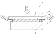
- FIG. 1 is a cross-sectional view showing a schematic configuration of an electrostatic chuck according to an embodiment of the present disclosure.
- FIG. 11 is a cross-sectional view showing a schematic configuration of another electrostatic chuck according to an embodiment of the present disclosure.
- Figures 1 and 2 are cross-sectional views showing the schematic configuration of an electrostatic chuck according to an embodiment of the present disclosure.
- an electrostatic chuck 1 includes a substrate 2 for attracting an object to be attracted, a base 3 for supporting the substrate 2, and an adhesive layer 4 for adhering the substrate 2 to the base 3.
- the adhesive layer 4 includes a first adhesive layer 4a located at the center of the substrate 2 and a second adhesive layer 4b located closer to an end of the substrate 2 than the first adhesive layer 4a.
- the electrostatic chuck 1 further includes a plasma protective layer 5 located closer to the end of the substrate 2 than the second adhesive layer 4b, and the plasma protective layer 5 is adhered to the second adhesive layer 4b.
- the substrate 2 is for adsorbing and holding an object to be adsorbed (not shown).
- the shape of the substrate 2 is not limited, and it can be disk-shaped or rectangular in shape to match the shape of the object to be adsorbed.
- the dimensions of the substrate 2 can also be set appropriately in accordance with the object to be adsorbed.
- the "object to be adsorbed” is also not limited, and can include various wafers for manufacturing semiconductor devices, flat panel display (FPD) panels and substrates, metal members, film members, glass members, and the like.
- Materials for the substrate 2 include ceramic substrates, silicon carbide substrates, and metal substrates made of aluminum, stainless steel, etc.
- the thickness of the substrate 2 is not particularly limited and can be within the range of 0.2 mm to 7 mm. In addition, if an internal electrode is provided on the substrate 2 as described below, the thickness of the substrate 2 may be within the range of 3 mm to 10 mm.
- the base 3 supports the substrate 2 and also has a cooling function.
- the shape, material, thickness, and other aspects of the base 3 can be appropriately designed to suit the application.
- the material of the base 3 can be ceramic, metal, or a combination thereof.
- the adhesive layer 4 adheres the substrate 2 to the base 3.
- the adhesive layer 4 has a first adhesive layer 4a located toward the center of the substrate 2 and a second adhesive layer 4b located closer to the end of the substrate 2 than the first adhesive layer 4a (FIGS. 1 and 2).
- the thickness of the adhesive layer 4 is not particularly limited, but is preferably 50 ⁇ m to 500 ⁇ m, and more preferably 100 ⁇ m to 300 ⁇ m. If the thickness of the adhesive layer 4 is within this range, the adhesive layer 4 can adequately withstand the stress caused by the difference in the linear expansion coefficient between the substrate and the base.
- the Young's modulus of the first adhesive layer 4a at 25° C. is preferably 2000 to 5000 MPa, and more preferably 3000 to 4000 MPa. If the Young's modulus of the first adhesive layer 4a at 25° C. is within this range, the moderately hard first adhesive layer 4a exhibits sufficient adhesive strength, and furthermore, the flexibility of the second adhesive layer 4b described below is prominent, and the second adhesive layer 4b effectively absorbs stress due to expansion and contraction of the substrate 2 and the base 3, thereby making it possible to suppress cracking and peeling of the electrostatic chuck.
- the first adhesive layer 4a preferably contains a thermally conductive filler.
- a thermally conductive filler By containing a thermally conductive filler, it is possible to achieve both adhesiveness and thermal conductivity.
- thermally conductive fillers include, but are not limited to, alumina, aluminum nitride, silicon carbide, boron nitride, carbon black, and carbon nanotubes. There are also no particular limitations on the amount, shape, etc. of the thermally conductive filler.
- the second adhesive layer 4b has a Young's modulus of 1 MPa or more at 100° C. and a Young's modulus of 1000 MPa or less at 25° C. Since the Young's modulus at 100° C. is 1 MPa or more, the second adhesive layer 4b has an appropriate fluidity, and deformation or cracking of the plasma protective layer 5 caused by excessively high fluidity can be suppressed. On the other hand, since the Young's modulus at 25° C. is 1000 MPa or less, deformation or cracking of the electrostatic chuck can be suppressed when a difference in the linear expansion coefficient between the substrate 2 and the base 3 occurs.
- the upper limit of the Young's modulus of the second adhesive layer 4b at 100°C is, for example, 100 MPa or less, and the lower limit of the Young's modulus at 25°C is 10 MPa or more. It is also preferable that the Young's modulus of the second adhesive layer 4b at 100°C is 10 MPa or more, and the Young's modulus at 25°C is 500 MPa or less.
- Such a second adhesive layer 4b is expected to more reliably suppress cracking of the electrostatic chuck caused by differences in the linear expansion coefficient between the substrate 2 and the base 3.
- Suitable materials for the second adhesive layer 4b include thermoplastic elastomers, thermosetting elastomers, epoxy resins, urethane resins, polyester resins, polyimide resins, polyamide resins, fluororubber, acrylic rubber, silicone rubber, and urethane rubber.
- the second adhesive layer 4b may be used in combination with a thermally conductive filler as appropriate.
- thermally conductive fillers include alumina, aluminum nitride, silicon carbide, boron nitride, carbon black, and carbon nanotubes.
- the method for measuring Young's modulus is not particularly limited, but a dynamic viscoelasticity measurement method can be used.
- a Rheovibron DDV-II manufactured by Orientec Co., Ltd.
- Young's modulus can be measured at 25°C and 100°C under set conditions of a vibration frequency of 11 Hz and a heating rate of 5°C/min.
- the volume ratio of the first adhesive layer 4a to the second adhesive layer 4b in the horizontal direction is not limited to that shown in Figures 1 and 2, and can be designed as appropriate so that the first adhesive layer 4a bonds the substrate 2 and the base 3, while the second adhesive layer 4b absorbs stress due to expansion and contraction of the substrate 2 and the base 3.
- the ratio of the volume of the second adhesive layer 4b to the volume of the first adhesive layer 4a is 0.01 volume % or more and 20 volume % or less, and preferably 1 volume % or more and 10 volume % or less.
- the first adhesive layer 4a and the second adhesive layer 4b do not necessarily have to be formed in a concentric shape.
- the length of the adhesive layer 4 in the horizontal direction (the total length of the first adhesive layer 4a and the second adhesive layer 4b) can also be designed as appropriate.
- the second adhesive layer 4b can be formed so as to have a recessed shape toward the center of the substrate 2.
- the second adhesive layer 4b (as well as the plasma protection layer 5 described later) is recessed in an angular shape, but it may also be formed in an arc shape.
- the plasma protective layer 5 adheres to the second adhesive layer 4b to protect the adhesive layer 4 from plasma.
- the material of the plasma protective layer 5 may include an inorganic material.
- the inorganic material include at least one of yttrium, aluminum, zirconium, calcium, and magnesium, and may be an oxide, hydroxide, or mixture of these elements, and the mixture may include hydroxyapatite.
- the plasma protective layer 5 may be disposed closer to the center of the substrate 2 than the end of the substrate 2 (FIG. 2). Specifically, the plasma protective layer 5 may be disposed at a distance in the range of 50 ⁇ m to 1000 ⁇ m from the end of the substrate 2 toward the side closer to the center of the substrate 2. For example, if the plasma protective layer 5 is disposed at a position 1000 ⁇ m away from the end of the substrate 2 (start point: 0 ⁇ m) shown in FIG. 2, deterioration of the plasma protective layer 5 due to plasma, etc. can be suppressed, and the adhesive layer 4 is also disposed farther away from the plasma source, so that it is more reliably protected. In this case, the horizontal length of the substrate 2 can be within the range of 30 mm to 600 mm.
- the thickness of the plasma protective layer 5 is not particularly limited, but can be in the range of 1 ⁇ m to 300 ⁇ m, and is preferably 20 ⁇ m to 150 ⁇ m. Such a plasma protective layer 5 can protect the adhesive layer 4 from plasma while suppressing cracking and peeling of the plasma protective layer 5 itself.
- an internal electrode (not shown) can be provided on the substrate 2 in order to apply a voltage to generate an electrostatic force (Coulomb force) to attract an object to be attracted.
- an internal electrode may be provided on the base 3.
- the internal electrode is not particularly limited as long as it is made of a conductive material that can exert an electrostatic adsorption force when a voltage is applied.
- a conductive material that can exert an electrostatic adsorption force when a voltage is applied.
- thin films made of metals such as copper, aluminum, gold, silver, platinum, chromium, nickel, and tungsten, and thin films made of at least two metals selected from the above metals are preferably used as the internal electrode.
- Examples of such thin metal films include those formed by deposition, plating, sputtering, etc., and those formed by applying and drying a conductive paste, specifically, metal foils such as copper foil.
- the electrostatic chuck 1 can be manufactured, for example, as follows. First, the substrate 2 and the base 3 are prepared. At this time, as described above, a metal such as copper is patterned on either the substrate 2 or the base 3 to form an internal electrode. Next, the substrate 2 and the base 3 are bonded via the adhesive layer 4 (in this state, the first adhesive layer 4a). At this time, the formation range of the first adhesive layer 4a is determined so that a gap is formed at a predetermined distance from each end of the substrate 2 and the base 3. The second adhesive layer 4b and the plasma protective layer 5 are formed in this gap. Next, the plasma protective layer 5 is formed so as to close this gap.
- a coating liquid that becomes the second adhesive layer 4b is injected between the substrate 2, the base 3, the first adhesive layer 4a, and the plasma protective layer 5 by utilizing surface tension. After this, the second adhesive layer 4b and the plasma protective layer 5 protruding from the end of the substrate 2 are scraped off, and the electrostatic chuck 1 as shown in FIG. 1 or FIG. 2 can be obtained.
- the electrostatic chuck 1 can also be manufactured by a manufacturing method of the embodiment described later.
- the electrostatic chuck 1 generates a Coulomb force by applying a voltage to the internal electrodes embedded in the substrate 2 or base 3, and attracts the object to be attracted.
- the electrostatic chuck 1 can be used to attract a wafer (object to be attracted) in a dry etching or CVD process in a semiconductor manufacturing process.
- the electrostatic chuck 1 according to this embodiment can protect the adhesive layer 4 from plasma by the plasma protection layer 5.
- the second adhesive layer 4b can follow the thermal expansion, so that cracks in the electrostatic chuck caused by the difference in linear expansion coefficient with the substrate 2 or base 3 can be suppressed.
- the life and productivity of the electrostatic chuck 1 itself are improved compared to conventional electrostatic chucks.
- the electrostatic chuck 1 of the present embodiment configured as described above, includes a substrate 2 for adsorbing an object to be adsorbed, a base supporting the substrate 2, and an adhesive layer 4 for adhering the substrate 2 to the base 3.
- the adhesive layer 4 includes a first adhesive layer 4a located at the center of the substrate 2, and a second adhesive layer 4b located closer to the end of the substrate 2 than the first adhesive layer 4a.
- a plasma protective layer 5 is provided closer to the end of the substrate 2 than the second adhesive layer 4b, and the plasma protective layer 5 is adhered to the second adhesive layer 4b.
- the Young's modulus of the second adhesive layer 4b at 100°C is 1 MPa or more, and the Young's modulus at 25°C is 1000 MPa or less.
- the second adhesive layer 4b has an appropriate fluidity, and therefore deformation or cracking of the electrostatic chuck due to excessive fluidity can be suppressed. Furthermore, even if the substrate 2 or base 3 expands or contracts due to temperature changes in the surrounding environment caused by plasma etching or the like, the second adhesive layer 4b absorbs the stress caused by the expansion and contraction, thereby suppressing deformation or cracking of the electrostatic chuck due to differences in the linear expansion coefficient between the substrate 2 and base 3.
- the Young's modulus of the second adhesive layer 4b at 100°C may be 10 MPa or more, and the Young's modulus at 25°C may be 500 MPa or less.
- the plasma protective layer 5 may be disposed closer to the center of the substrate 2 than the edge of the substrate 2, and further, the plasma protective layer 5 may be disposed at a distance within a range of 50 ⁇ m to 1000 ⁇ m from the edge of the substrate 2 toward the side closer to the center of the substrate 2 (FIG. 2). In this way, the plasma protective layer 5 does not extend beyond the edge of the substrate 2, so that deterioration of the plasma protective layer 5 due to plasma, etc. can be suppressed, and the adhesive layer 4 is less likely to be exposed to plasma and is more reliably protected.
- the first adhesive layer 4a may contain a thermally conductive filler. In this way, it is possible to suppress variations in thickness and temperature distribution within the first adhesive layer 4a, and to release heat from the surrounding environment.
- the plasma protection layer 5 can contain an inorganic material.
- this inorganic material may be composed of at least one of yttrium, aluminum, zirconium, calcium, and magnesium. Such a material can exhibit favorable plasma resistance.
- the electrostatic chuck 1 according to this embodiment is not limited to the above-mentioned aspects and combinations.
- the substrate 2 or base 3 may have two internal electrodes instead of just one.
- the plasma protective layer 5 is provided on the edge side of the substrate 2, but the plasma protective layer 5 may be provided along the entire periphery of the substrate 2, not just along a part of the edge of the substrate 2.
- the plasma protective layer 5 (second adhesive layer 4b) may also be provided symmetrically (for example, in four places) on the periphery of the substrate 2.
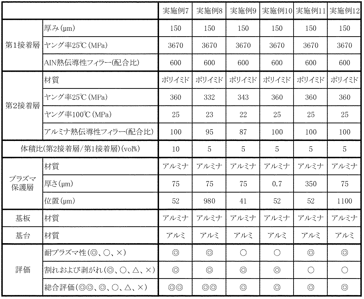
- Example 1 The evaluation sample was manufactured using the materials shown in Table 1. That is, an alumina substrate (300 mm ⁇ disk-shaped, 3.0 mm thick) and an aluminum base (295 mm ⁇ disk-shaped, 15 mm thick) were prepared, and the silicone adhesive was applied concentrically to the substrate from the end of the substrate toward the center for a length of 4.0 mm so that the uncoated portion was on the entire periphery, and the substrate was bonded to the base. The thickness of the silicone adhesive was 150 ⁇ m. Next, the polyimide adhesive was applied to the entire periphery of the silicone adhesive, and the polyimide adhesive was left to stand in a thermostatic chamber set at 120 ° C for 10 minutes to dry the polyimide adhesive.
- the thickness of the polyimide adhesive after drying was 150 ⁇ m. Then, a plasma spraying device was used to spray alumina particles on the entire periphery of the polyimide adhesive, and the alumina particles were sprayed so that a plasma protective layer having a thickness of 75 ⁇ m was formed at the position shown in Table 1 (substrate end: 0 ⁇ m).
- the polyimide adhesive and the plasma protective layer protruding from the outer periphery of the substrate and base were polished using an electric mill to obtain a sample for evaluation.
- the silicone adhesive and polyimide adhesive used in each example were prepared as follows.
- a commercially available silicone adhesive (“One-component additive RTV silicone rubber KE-8101” manufactured by Shin-Etsu Chemical Co., Ltd.) was mixed and stirred with an aluminum nitride filler ("AlN filler FAN-f05” manufactured by Furukawa Electronics Co., Ltd., average particle size 3 to 10 ⁇ m) in the compounding ratios shown in Tables 1 to 4 (amount compounded relative to 100 parts by weight of silicone adhesive), to obtain silicone-based adhesives exhibiting Young's moduli as shown in Tables 1 to 4.
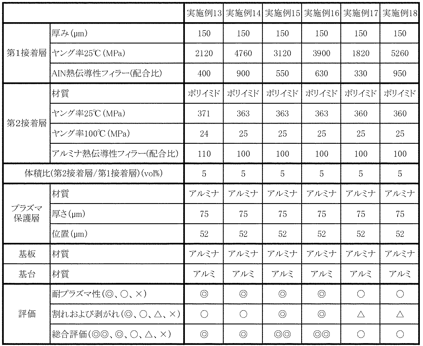
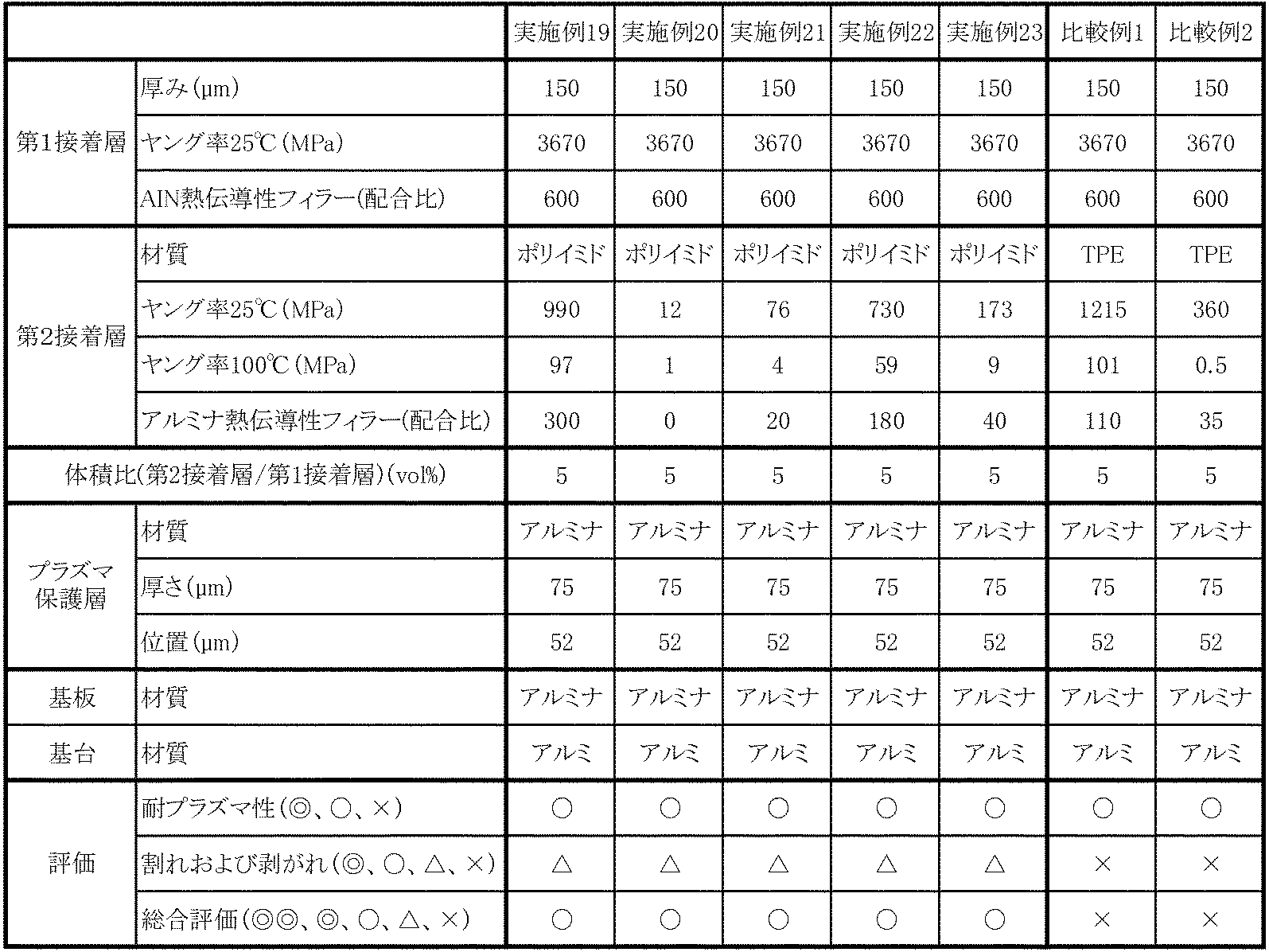
- Example 2 to 5 ⁇ Examples 2 to 5, 8, 9, 11 to 23> As shown in Tables 1 to 4, evaluation samples were obtained in the same manner as in Example 1.
- Example 6 An evaluation sample was obtained in the same manner as in Example 1, except that the silicone adhesive was applied concentrically to the substrate so that an uncoated portion was left over the entire outer periphery for a length of 2.0 mm from the edge of the substrate toward the center.
- Example 7 An evaluation sample was obtained in the same manner as in Example 1, except that the silicone adhesive was applied concentrically to the substrate so that an uncoated portion was left over the entire periphery for a length of 7.5 mm from the edge of the substrate toward the center.
- Example 10 A sample for evaluation was obtained in the same manner as in Example 1, except for the formation of the plasma protective layer. That is, a 20% by mass solution of aluminum nitrate nonahydrate in 1,3-butanediol was prepared and applied to the entire outer periphery of the polyimide-based adhesive by a spray method. Thereafter, the sample was placed in a thermostatic chamber set at 200°C and dried for 2 hours to form a plasma protective layer. The polyimide-based adhesive and the plasma protective layer protruding from the outer periphery of the substrate and base were polished using an electric grinder to obtain a sample for evaluation.
- thermoplastic ethylene (TPE) adhesive was used instead of a polyimide adhesive. That is, a styrene-based thermoplastic elastomer (TPE) (Kraton G1651, manufactured by Kraton) was dissolved in toluene to prepare a 25% solution, and then alumina filler (Taimei Chemical Industry Co., Ltd.
- Taimicron TM-UF average particle size 0.09 ⁇ m
- Examples 13-16 Furthermore, a comparison of Examples 13-16 with Examples 17-18 showed that when the Young's modulus (25°C) of the first adhesive layer was within the range of 2000-5000 MPa, the plasma resistance and heat cycle resistance were even better. When the Young's modulus (25°C) of the first adhesive layer was within the range of 3000-4000 MPa, the plasma resistance and heat cycle resistance were particularly good.
- Examples 1 to 8 showed that both plasma resistance and heat cycle resistance were good even when the plasma protective layer was positioned at a distance within a range of 50 ⁇ m to 1000 ⁇ m from the edge of the substrate toward the side closer to the center of the substrate.
- Example 1 Furthermore, for example, a comparison between Example 1 and Examples 10-11 revealed that when the thickness of the plasma protective layer 5 is in the range of 1 ⁇ m to 300 ⁇ m, a good balance of plasma resistance and heat cycle resistance can be achieved.
Landscapes
- Physics & Mathematics (AREA)
- Engineering & Computer Science (AREA)
- Plasma & Fusion (AREA)
- Chemical & Material Sciences (AREA)
- Analytical Chemistry (AREA)
- Container, Conveyance, Adherence, Positioning, Of Wafer (AREA)
- Laminated Bodies (AREA)
Abstract
Description
被吸着物を吸着するための基板と、
前記基板を支持する基台と、
前記基板を前記基台に接着する接着層と、
を備え、
前記接着層は、前記基板の中央側に位置する第1接着層と、前記第1接着層よりも前記基板の端部に近い側に位置する第2接着層とを有しており、
前記第2接着層よりも前記基板の端部に近い側にプラズマ保護層が設けられており、前記プラズマ保護層は前記第2接着層に接着しており、
前記第2接着層の100℃におけるヤング率は1MPa以上であり、25℃におけるヤング率は1000MPa以下である。
前記第2接着層の100℃におけるヤング率は10MPa以上であり、25℃におけるヤング率は500MPa以下であってもよい。
前記第1接着層の25℃におけるヤング率は2000~5000MPaの範囲内であってもよい。
前記プラズマ保護層は、前記基板の端部よりも前記基板の中央に近い側に配置されてもよい。
前記プラズマ保護層は、前記基板の端部から前記基板の中央に近い側に向かって50μm~1000μmの範囲内の距離の箇所に配置されてもよい。
前記第2接着層は、前記基板の中央側に窪んだ形状となっていてもよい。
前記第1接着層は熱伝導性フィラーを含んでもよい。
前記プラズマ保護層は無機材料を含んでもよい。
前記無機材料は、イットリウム、アルミニウム、ジルコニウム、カルシウム、およびマグネシウムのうち少なくとも何れかのものから構成されてもよい。
図1および図2に示すように、本実施の形態による静電チャック1は、被吸着物を吸着するための基板2と、基板2を支持する基台3と、基板2を基台3に接着する接着層4と、を備える。接着層4は、基板2の中央側に位置する第1接着層4aと、第1接着層4aよりも基板2の端部に近い側に位置する第2接着層4bとを有する。さらに、静電チャック1は、第2接着層4bよりも基板2の端部に近い側にプラズマ保護層5を備え、プラズマ保護層5は第2接着層4bに接着している。
基板2は、被吸着物(図示せず)を吸着して保持するためのものである。基板2の形状は限定されず、被吸着物の形状に合わせて円板状や四角形状にすることもできる。基板2の寸法も、被吸着物に合わせて適宜設定できる。なお、「被吸着物」も限定されず、半導体装置を製造するための様々なウェーハ、フラットパネルディスプレイ(FPD)パネルや基板、金属部材、フィルム部材、ガラス部材等を包含し得る。
基台3は、基板2を支持するものであり、冷却機能も有する。基台3の形状、材料、厚さ等は用途に合わせて適宜設計変更できる。例えば、基台3の材料としては、セラミック、金属、およびこれらを組み合わせたものが挙げられる。
接着層4は、基板2を基台3に接着するものである。本実施の形態による静電チャック1において、接着層4は、基板2の中央側に位置する第1接着層4aと、第1接着層4aよりも基板2の端部に近い側に位置する第2接着層4bとを有している(図1~図2)。
第1接着層4aの25℃におけるヤング率は2000~5000MPaであることが好ましく、3000~4000MPaであることがより好ましい。第1接着層4aの25℃におけるヤング率がこの範囲であれば、適度に固い第1接着層4aにより十分な接着力が発揮され、さらに、後述する第2接着層4bの柔軟性が際立ち、基板2や基台3の膨張収縮による応力を第2接着層4bが効果的に吸収することになり、静電チャックの割れや剥がれを抑制することができる。
第2接着層4bの100℃におけるヤング率は1MPa以上であり、25℃におけるヤング率は1000MPa以下である。100℃におけるヤング率が1MPa以上であることにより、第2接着層4bは適度な流動性を有し、流動性が高すぎることによるプラズマ保護層5の変形や割れを抑制できる。一方、25℃におけるヤング率が1000MPa以下であることにより、基板2と基台3の線膨張率差が生じた際に、静電チャックの変形や割れを抑制できる。
プラズマ保護層5は、第2接着層4bに接着して、接着層4をプラズマから保護するものである。プラズマ保護層5の材料として、無機材料を含むことができる。無機材料の例として、イットリウム、アルミニウム、ジルコニウム、カルシウム、およびマグネシウムのうち少なくとも1種を含むものが挙げられ、これらの酸化物、水酸化物、またはこれらの混合物でもよく、混合物中にはハイドロキシアパタイトを含んでもよい。
本実施の形態による静電チャック1において、電圧を印加して静電気力(クーロン力)を発生させて被吸着物を吸着するために内部電極(図示せず)を基板2に設けることができる。或いは、このような内部電極を基台3に設けてもよい。
静電チャック1は、例えば、以下のように製造できる。まず、基板2および基台3を用意する。このとき、上述したように、基板2か基台3のいずれかに、銅等の金属をパターン形成して内部電極を形成させる。次に、基板2と基台3を、接着層4(この状態では、第1接着層4a)を介して接着する。このとき、基板2と基台3のそれぞれの端部から所定の距離に隙間ができるように第1接着層4aの形成範囲を決定する。この隙間に第2接着層4bおよびプラズマ保護層5が形成されることとなる。次に、この隙間を塞ぐようにプラズマ保護層5を形成する。次に、表面張力を利用して、基板2、基台3、第1接着層4a、プラズマ保護層5の間に、第2接着層4bとなる塗液を注入する。この後、基板2の端部から突出する第2接着層4bやプラズマ保護層5を削り、図1または図2に示すような静電チャック1を得ることができる。また、後述する実施例の製法により静電チャック1を製造することもできる。
表1に示す材料を用いて評価用サンプルを製造した。すなわち、アルミナ基板(300mmφ円盤状、3.0mm厚さ)およびアルミニウム基台(295mmφ円盤状、15mm厚さ)を用意し、基板の端部から4.0mm長さ中心部に向かって未塗布部が外周全体にできるようにシリコーン系接着剤を基板に対して同心円状に塗布し、基台と接着させた。シリコーン系接着剤の厚みは150μmであった。次いで、ポリイミド系接着剤をシリコーン系接着剤の外周全体に塗布し、120℃に設定した恒温槽に10分間静置し、ポリイミド系接着剤を乾燥させた。乾燥後のポリイミド系接着剤の厚みは150μmであった。その後、プラズマ溶射装置を用いて、ポリイミド系接着剤の外周全体にアルミナ粒子を溶射し、75μm厚さのプラズマ保護層が表1に示す位置(基板端部:0μm)に形成されるようにアルミナ粒子を溶射した。基板と基台の外周から突出するポリイミド系接着剤およびプラズマ保護層を電動リューターを用いて研磨し、評価用サンプルを得た。
市販のシリコーン接着剤(信越化学社製「1液付加型RTVシリコーンゴム KE-8101」)に窒化アルミニウムフィラー(古河電子社「AlNフィラー FAN-f05」、平均粒径3~10μm)を表1-表4に示した配合比(シリコーン接着剤100重量部に対する配合量)で混合・撹拌し、表1-表4に示すようなヤング率を発揮する各シリコーン系接着剤を得た。
市販のポリイミド接着剤(T&K TOKA社製「溶剤可溶型熱可塑性ポリイミド PI-1」をテトラヒドロフランに溶解し、25%溶液を作製した。その後、アルミナフィラー(大明化学工業社「タイミクロンTM-UF」、平均粒径0.09μm)を表1-表4に示した配合比(ポリイミド接着剤100重量部に対する配合量)で混合・撹拌し、表1-表4に示すようなヤング率を発揮する各ポリイミド系接着剤を得た。
表1-表4に示すように、実施例1と同様に評価用サンプルを得た。
基板の端部から2.0mm長さ中心部に向かって未塗布部が外周全体にできるようにシリコーン系接着剤を基板に対して同心円状に塗布した以外は、実施例1と同様に評価用サンプルを得た。
基板の端部から7.5mm長さ中心部に向かって未塗布部が外周全体にできるようにシリコーン系接着剤を基板に対して同心円状に塗布した以外は、実施例1と同様に評価用サンプルを得た。
プラズマ保護層の形成以外は、実施例1と同様に評価用サンプルを得た。すなわち、硝酸アルミニウム九水和物の1,3-ブタンジオール20質量%溶液を準備し、スプレー法にてポリイミド系接着剤の外周全体に塗布した。その後、200℃に設定した恒温槽に投入し2時間乾燥し、プラズマ保護層を形成した。基板と基台の外周から突出するポリイミド系接着剤およびプラズマ保護層を電動リューターを用いて研磨し、評価用サンプルを得た。
表4に示すように、実施例1と同様に評価用サンプルを得た。比較例1、2ではポリイミド系接着剤の代わりに、熱可塑(TPE)系接着剤を用いた。すなわち、スチレン系熱可塑性エラストマー(TPE)(クレイトン社製、クレイトンG1651)をトルエンに溶解し、25%溶液を作製した後、アルミナフィラー(大明化学工業社「タイミクロンTM-UF」、平均粒径0.09μm)を表4に示した配合比(溶液100重量部に対する配合量)で混合・撹拌し、表4に示すようなヤング率を発揮する各TPE系接着剤を得た。
(耐プラズマ性の評価)
実施例1~23、比較例1、2の耐プラズマ性の評価を行った。すなわち、平行平板型RIE装置に各評価用サンプルを設置した後、真空下(20Pa以下)、高周波電源(出力250W)にて、酸素ガス(10sccm)および四フッ化炭素ガス(40sccm)を導入し、24時間暴露後の各評価用サンプル外周の表面状態の変化を目視にて観察した。外周全体にプラズマ層が損傷なく残っているものを「◎」、プラズマ保護層の一部に割れがあるものの、外周全体にプラズマ保護層が残っているものを「〇」、プラズマ保護層に割れ、剥がれが生じて一部欠損していたものを「×」とした。
実施例1~23、比較例1、2の各評価サンプルの冷熱サイクル後の割れおよび剥がれの評価を行った。すなわち各評価サンプルを0℃に設定した恒温槽(エスペック社製 TCC‐151W)に投入した。その後、昇温速度50℃/時間で120℃まで昇温させた後、すぐに降温速度50℃/時間で0℃まで降温させる工程を200サイクル行った。200サイクル終了後、各評価サンプルを恒温槽から取り出し、各評価サンプルの外観(プラズマ保護層、基板、基台)を観察した。全てにおいて割れおよび剥がれが発生しなかったものを「◎」、プラズマ保護層の割れのみ発生したものを「〇」、プラズマ保護層の一部に剥離が発生したものを「△」、基板、基台の割れまたは剥離が発生したものを「×」とした。
耐プラズマ性の評価と割れおよび剥がれの評価のうち、2つの評価が「◎」の場合「◎◎」とし、一方が「〇」または「△」で他方が「◎」の場合「◎」とした。また、2つの評価が「〇」の場合、一方が「〇」で他方が「△」の場合も「〇」とした。2つの評価が「△」の場合、「△」とした。1つでも「×」と評価された場合は、「×」とした。

Claims (9)
- 被吸着物を吸着するための基板と、
前記基板を支持する基台と、
前記基板を前記基台に接着する接着層と、
を備え、
前記接着層は、前記基板の中央側に位置する第1接着層と、前記第1接着層よりも前記基板の端部に近い側に位置する第2接着層とを有しており、
前記第2接着層よりも前記基板の端部に近い側にプラズマ保護層が設けられており、前記プラズマ保護層は前記第2接着層に接着しており、
前記第2接着層の100℃におけるヤング率は1MPa以上であり、25℃におけるヤング率は1000MPa以下である、静電チャック。 - 前記第2接着層の100℃におけるヤング率は10MPa以上であり、25℃におけるヤング率は500MPa以下である、請求項1記載の静電チャック。
- 前記第1接着層の25℃におけるヤング率は2000~5000MPaの範囲内である、請求項1記載の静電チャック。
- 前記プラズマ保護層は、前記基板の端部よりも前記基板の中央に近い側に配置されている、請求項1記載の静電チャック。
- 前記プラズマ保護層は、前記基板の端部から前記基板の中央に近い側に向かって50μm~1000μmの範囲内の距離の箇所に配置されている、請求項4記載の静電チャック。
- 前記第2接着層は、前記基板の中央側に窪んだ形状となっている、請求項1記載の静電チャック。
- 前記第1接着層は熱伝導性フィラーを含む、請求項1記載の静電チャック。
- 前記プラズマ保護層は無機材料を含む、請求項1乃至7のいずれか一項に記載の静電チャック。
- 前記無機材料は、イットリウム、アルミニウム、ジルコニウム、カルシウム、およびマグネシウムのうち少なくとも何れかのものから構成されている、請求項8記載の静電チャック。
Priority Applications (3)
| Application Number | Priority Date | Filing Date | Title |
|---|---|---|---|
| CN202480043210.0A CN121420684A (zh) | 2023-06-30 | 2024-06-21 | 静电卡盘 |
| EP24831841.2A EP4738431A1 (en) | 2023-06-30 | 2024-06-21 | Electrostatic chuck |
| KR1020257035396A KR20250168449A (ko) | 2023-06-30 | 2024-06-21 | 정전척 |
Applications Claiming Priority (2)
| Application Number | Priority Date | Filing Date | Title |
|---|---|---|---|
| JP2023-108894 | 2023-06-30 | ||
| JP2023108894 | 2023-06-30 |
Publications (1)
| Publication Number | Publication Date |
|---|---|
| WO2025004980A1 true WO2025004980A1 (ja) | 2025-01-02 |
Family
ID=93938526
Family Applications (1)
| Application Number | Title | Priority Date | Filing Date |
|---|---|---|---|
| PCT/JP2024/022511 Ceased WO2025004980A1 (ja) | 2023-06-30 | 2024-06-21 | 静電チャック |
Country Status (5)
| Country | Link |
|---|---|
| EP (1) | EP4738431A1 (ja) |
| KR (1) | KR20250168449A (ja) |
| CN (1) | CN121420684A (ja) |
| TW (1) | TW202510187A (ja) |
| WO (1) | WO2025004980A1 (ja) |
Citations (5)
| Publication number | Priority date | Publication date | Assignee | Title |
|---|---|---|---|---|
| JP2006013302A (ja) * | 2004-06-29 | 2006-01-12 | Ngk Insulators Ltd | 基板載置装置及び基板温度調整方法 |
| WO2016132909A1 (ja) | 2015-02-18 | 2016-08-25 | 住友大阪セメント株式会社 | 静電チャック装置及び半導体製造装置 |
| JP2020027914A (ja) * | 2018-08-17 | 2020-02-20 | 日本特殊陶業株式会社 | 保持装置 |
| JP2020047746A (ja) * | 2018-09-19 | 2020-03-26 | 日本特殊陶業株式会社 | 保持装置 |
| JP2020053707A (ja) * | 2018-09-28 | 2020-04-02 | 日本特殊陶業株式会社 | 半導体製造用部品 |
-
2024
- 2024-06-21 KR KR1020257035396A patent/KR20250168449A/ko active Pending
- 2024-06-21 EP EP24831841.2A patent/EP4738431A1/en active Pending
- 2024-06-21 WO PCT/JP2024/022511 patent/WO2025004980A1/ja not_active Ceased
- 2024-06-21 CN CN202480043210.0A patent/CN121420684A/zh active Pending
- 2024-06-26 TW TW113123850A patent/TW202510187A/zh unknown
Patent Citations (5)
| Publication number | Priority date | Publication date | Assignee | Title |
|---|---|---|---|---|
| JP2006013302A (ja) * | 2004-06-29 | 2006-01-12 | Ngk Insulators Ltd | 基板載置装置及び基板温度調整方法 |
| WO2016132909A1 (ja) | 2015-02-18 | 2016-08-25 | 住友大阪セメント株式会社 | 静電チャック装置及び半導体製造装置 |
| JP2020027914A (ja) * | 2018-08-17 | 2020-02-20 | 日本特殊陶業株式会社 | 保持装置 |
| JP2020047746A (ja) * | 2018-09-19 | 2020-03-26 | 日本特殊陶業株式会社 | 保持装置 |
| JP2020053707A (ja) * | 2018-09-28 | 2020-04-02 | 日本特殊陶業株式会社 | 半導体製造用部品 |
Also Published As
| Publication number | Publication date |
|---|---|
| KR20250168449A (ko) | 2025-12-02 |
| CN121420684A (zh) | 2026-01-27 |
| EP4738431A1 (en) | 2026-05-06 |
| TW202510187A (zh) | 2025-03-01 |
Similar Documents
| Publication | Publication Date | Title |
|---|---|---|
| JP6627936B1 (ja) | 静電チャック装置および静電チャック装置の製造方法 | |
| TWI467691B (zh) | Electrostatic chuck and its manufacturing method | |
| US9466518B2 (en) | Electrostatic chuck device | |
| JP4942471B2 (ja) | サセプタおよびこれを用いたウェハの処理方法 | |
| JP6702385B2 (ja) | 静電チャック装置 | |
| JP2013187477A (ja) | 静電チャック装置 | |
| CN111446197A (zh) | 静电吸盘和包括其的静电吸盘装置 | |
| US10957573B2 (en) | Electrostatic chuck device including a heating member | |
| JP2521471B2 (ja) | 静電吸着装置 | |
| JPH10270540A (ja) | 静電チャックデバイスおよび静電チャック用基台 | |
| WO2025004980A1 (ja) | 静電チャック | |
| JP6510356B2 (ja) | ウエハ支持装置 | |
| TWI813840B (zh) | 靜電夾頭裝置 | |
| JPH10209257A (ja) | 静電チャック装置およびその製造方法 | |
| JPH10209256A (ja) | 静電チャック装置およびその製造方法 | |
| JP2004356350A (ja) | 静電チャック | |
| JP4890428B2 (ja) | 静電チャック | |
| CN114144873B (zh) | 着脱装置 | |
| TWI921310B (zh) | 著脫裝置 | |
| JP2004031599A (ja) | 静電チャック | |
| JPH06302677A (ja) | セラミックス製静電チャック | |
| TW201841739A (zh) | 電子元件的載片以及使用其的用於形成薄膜的裝置 | |
| TW202537034A (zh) | 靜電夾頭 | |
| JPH06326178A (ja) | 静電吸着装置 |
Legal Events
| Date | Code | Title | Description |
|---|---|---|---|
| 121 | Ep: the epo has been informed by wipo that ep was designated in this application |
Ref document number: 24831841 Country of ref document: EP Kind code of ref document: A1 |
|
| ENP | Entry into the national phase |
Ref document number: 2025530079 Country of ref document: JP Kind code of ref document: A |
|
| WWE | Wipo information: entry into national phase |
Ref document number: 2025530079 Country of ref document: JP |
|
| ENP | Entry into the national phase |
Ref document number: 1020257035396 Country of ref document: KR Free format text: ST27 STATUS EVENT CODE: A-0-1-A10-A15-NAP-PA0105 (AS PROVIDED BY THE NATIONAL OFFICE) |
|
| WWE | Wipo information: entry into national phase |
Ref document number: KR1020257035396 Country of ref document: KR Ref document number: 1020257035396 Country of ref document: KR |
|
| WWP | Wipo information: published in national office |
Ref document number: 1020257035396 Country of ref document: KR |
|
| WWE | Wipo information: entry into national phase |
Ref document number: 202517132290 Country of ref document: IN |
|
| WWP | Wipo information: published in national office |
Ref document number: 202517132290 Country of ref document: IN |
|
| WWE | Wipo information: entry into national phase |
Ref document number: 2024831841 Country of ref document: EP |
|
| NENP | Non-entry into the national phase |
Ref country code: DE |
|
| ENP | Entry into the national phase |
Ref document number: 2024831841 Country of ref document: EP Effective date: 20260130 |
|
| ENP | Entry into the national phase |
Ref document number: 2024831841 Country of ref document: EP Effective date: 20260130 |