WO2025004788A1 - 炭化珪素エピタキシャル基板、炭化珪素半導体装置の製造方法、および炭化珪素半導体装置 - Google Patents
炭化珪素エピタキシャル基板、炭化珪素半導体装置の製造方法、および炭化珪素半導体装置 Download PDFInfo
- Publication number
- WO2025004788A1 WO2025004788A1 PCT/JP2024/021160 JP2024021160W WO2025004788A1 WO 2025004788 A1 WO2025004788 A1 WO 2025004788A1 JP 2024021160 W JP2024021160 W JP 2024021160W WO 2025004788 A1 WO2025004788 A1 WO 2025004788A1
- Authority
- WO
- WIPO (PCT)
- Prior art keywords
- silicon carbide
- basal plane
- density
- main surface
- carbide epitaxial
- Prior art date
- Legal status (The legal status is an assumption and is not a legal conclusion. Google has not performed a legal analysis and makes no representation as to the accuracy of the status listed.)
- Ceased
Links
Images








Classifications
-
- C—CHEMISTRY; METALLURGY
- C30—CRYSTAL GROWTH
- C30B—SINGLE-CRYSTAL GROWTH; UNIDIRECTIONAL SOLIDIFICATION OF EUTECTIC MATERIAL OR UNIDIRECTIONAL DEMIXING OF EUTECTOID MATERIAL; REFINING BY ZONE-MELTING OF MATERIAL; PRODUCTION OF A HOMOGENEOUS POLYCRYSTALLINE MATERIAL WITH DEFINED STRUCTURE; SINGLE CRYSTALS OR HOMOGENEOUS POLYCRYSTALLINE MATERIAL WITH DEFINED STRUCTURE; AFTER-TREATMENT OF SINGLE CRYSTALS OR A HOMOGENEOUS POLYCRYSTALLINE MATERIAL WITH DEFINED STRUCTURE; APPARATUS THEREFOR
- C30B29/00—Single crystals or homogeneous polycrystalline material with defined structure characterised by the material or by their shape
- C30B29/10—Inorganic compounds or compositions
- C30B29/36—Carbides
-
- H—ELECTRICITY
- H10—SEMICONDUCTOR DEVICES; ELECTRIC SOLID-STATE DEVICES NOT OTHERWISE PROVIDED FOR
- H10P—GENERIC PROCESSES OR APPARATUS FOR THE MANUFACTURE OR TREATMENT OF DEVICES COVERED BY CLASS H10
- H10P74/00—Testing or measuring during manufacture or treatment of wafers, substrates or devices
Definitions
- This disclosure relates to a silicon carbide epitaxial substrate, a method for manufacturing a silicon carbide semiconductor device, and a silicon carbide semiconductor device.
- This application claims priority to Japanese patent application No. 2023-105807, filed on June 28, 2023. All contents of the Japanese patent application are incorporated herein by reference.
- Patent Document 1 describes a SiC epitaxial wafer having a SiC single crystal substrate and an epitaxial layer provided on the SiC single crystal substrate.
- the epitaxial layer has a basal plane dislocation density of 0.1 dislocations/ cm2 or less extending from the SiC single crystal substrate to the outer surface.
- a silicon carbide epitaxial substrate includes a silicon carbide substrate, a buffer layer, and a drift layer.
- the buffer layer is provided on the silicon carbide substrate.
- the drift layer is provided on the buffer layer.
- the density of basal plane dislocations in the buffer layer is 10/ cm2 or less.
- the density of basal plane dislocations in the drift layer is 1/cm2 or less .
- a value obtained by dividing the density of basal plane dislocations in the buffer layer by the density of basal plane dislocations in the drift layer is 1 or more and 100 or less.
- FIG. 1 is a plan view showing a configuration of a silicon carbide epitaxial substrate according to this embodiment.
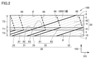
- FIG. 2 is a schematic cross-sectional view taken along line II-II in FIG.
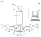
- FIG. 3 is a schematic diagram showing the configuration of a photoluminescence imaging device.
- FIG. 4 is a schematic plan view showing photoluminescence images of the first basal plane dislocation and the second basal plane dislocation.
- FIG. 5 is a schematic plan view showing the measurement positions of the first density and the second density.
- FIG. 6 is a cross-sectional view illustrating a configuration of an apparatus for manufacturing a silicon carbide epitaxial substrate according to this embodiment.
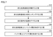
- FIG. 7 is a flow diagram that outlines the method for manufacturing a silicon carbide epitaxial substrate according to the present embodiment.
- FIG. 1 is a plan view showing a configuration of a silicon carbide epitaxial substrate according to this embodiment.
- FIG. 2 is a schematic cross-sectional view taken along line II-II in FIG.
- FIG. 8 is a schematic cross-sectional view showing a step of preparing a silicon carbide substrate.
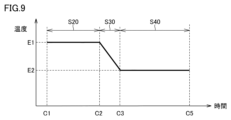
- FIG. 9 is a schematic diagram showing the change in temperature inside the reaction chamber over time.
- FIG. 10 is a schematic diagram showing the change over time in the flow rate of hydrogen gas and the flow rate of silane gas.
- FIG. 11 is a schematic cross-sectional view showing a step of forming a buffer layer on a silicon carbide substrate.
- FIG. 12 is a flowchart that roughly illustrates the method for manufacturing a silicon carbide semiconductor device according to this embodiment.
- FIG. 13 is a schematic cross-sectional view showing a step of preparing a silicon carbide epitaxial substrate.
- FIG. 14 is a schematic cross-sectional view showing a step of forming a body region.
- FIG. 15 is a schematic cross-sectional view showing a step of forming a source region.
- FIG. 16 is a schematic cross-sectional view showing a step of forming a trench in the first main surface of the silicon carbide epitaxial layer.
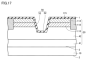
- FIG. 17 is a schematic cross-sectional view showing a step of forming a gate insulating film.
- FIG. 18 is a schematic cross-sectional view showing a step of forming a gate electrode and an interlayer insulating film.
- FIG. 19 is a schematic cross-sectional view showing the configuration of a silicon carbide semiconductor device according to this embodiment.
- FIG. 20 is a first photoluminescence image according to a comparative example.
- FIG. 21 is a first photoluminescence image according to an example.
- FIG. 22 is a second photoluminescence image according to a comparative example.
- FIG. 23 is a second photoluminescence image according to the example.
- An object of the present disclosure is to provide a silicon carbide epitaxial substrate, a method for manufacturing a silicon carbide semiconductor device, and a silicon carbide semiconductor device that are capable of suppressing deterioration in the reliability of a silicon carbide semiconductor device.
- Advantageous Effects of Invention it is possible to provide a silicon carbide epitaxial substrate capable of suppressing deterioration in the reliability of a silicon carbide semiconductor device, a method for manufacturing a silicon carbide semiconductor device, and a silicon carbide semiconductor device.
- an individual orientation is represented by [ ], a collective orientation by ⁇ >, an individual plane by ( ), and a collective plane by ⁇ ⁇ .
- a negative index in crystallography is usually represented by placing a "-" (bar) above the number, but in this specification, a negative index in crystallography is represented by placing a negative sign before the number.
- a silicon carbide epitaxial substrate includes a silicon carbide substrate, a buffer layer, and a drift layer.
- the buffer layer is provided on the silicon carbide substrate.
- the drift layer is provided on the buffer layer.
- the density of basal plane dislocations in the buffer layer is 10/cm2 or less.
- the density of basal plane dislocations in the drift layer is 1/cm2 or less.
- the value obtained by dividing the density of basal plane dislocations in the buffer layer by the density of basal plane dislocations in the drift layer is 1 or more and 100 or less. This makes it possible to suppress deterioration in the reliability of a silicon carbide semiconductor device manufactured using the silicon carbide epitaxial substrate.
- a silicon carbide epitaxial substrate includes a silicon carbide substrate, a buffer layer, and a drift layer.
- the buffer layer is provided on the silicon carbide substrate.
- the drift layer is provided on the buffer layer.
- the buffer layer has a basal plane dislocation density of 10 dislocations/cm2 or less .
- the drift layer has a basal plane dislocation density of 0 dislocations/ cm2 . This makes it possible to suppress deterioration in reliability of a silicon carbide semiconductor device manufactured using the silicon carbide epitaxial substrate.
- the buffer layer may have a thickness of 0.5 ⁇ m or more and 10 ⁇ m or less. This makes it possible to suppress the injection of holes into basal plane dislocations in the silicon carbide substrate.
- the drift layer may constitute the main surface.
- the diameter of the main surface may be 150 mm or more.
- the main surface may be inclined at an off angle of 1° or more and 8° or less with respect to the ⁇ 0001 ⁇ plane.
- the buffer layer may have a basal plane dislocation density of 0.01 dislocations/ cm2 or more.
- the method for manufacturing a silicon carbide semiconductor device includes the following steps: A silicon carbide epitaxial substrate according to any of (1) to (6) above is prepared. An electrode is formed on the silicon carbide epitaxial substrate. This makes it possible to suppress deterioration in the reliability of the silicon carbide semiconductor device 400.
- the silicon carbide semiconductor device includes the silicon carbide epitaxial substrate according to (2) above and an electrode provided on the silicon carbide epitaxial substrate. This makes it possible to suppress deterioration in the reliability of the silicon carbide semiconductor device.
- FIG. 1 is a plan view schematic diagram showing the configuration of a silicon carbide epitaxial substrate according to this embodiment.
- FIG. 2 is a cross-sectional schematic diagram taken along line II-II in FIG. 1.
- the silicon carbide epitaxial substrate 100 according to this embodiment mainly includes a silicon carbide substrate 10 and a silicon carbide epitaxial layer 20.
- the silicon carbide substrate 10 has a second main surface 2.
- the second main surface 2 is the back surface of the silicon carbide epitaxial substrate 100.
- the silicon carbide epitaxial layer 20 is provided on the silicon carbide substrate 10.
- the silicon carbide epitaxial layer 20 is in contact with the silicon carbide substrate 10.
- the silicon carbide epitaxial layer 20 has a first main surface 1.
- the first main surface 1 is the front surface of the silicon carbide epitaxial substrate 100.
- Silicon carbide epitaxial substrate 100 has an outer peripheral side surface 5. Outer peripheral side surface 5 is continuous with each of first main surface 1 and second main surface 2.
- the silicon carbide epitaxial substrate 100 has an outer peripheral edge 8.
- the outer peripheral edge 8 has, for example, an orientation flat 6 and an arc-shaped portion 7.
- the orientation flat 6 extends along a first direction 101.
- the orientation flat 6 is linear when viewed along a straight line perpendicular to the first main surface 1.
- the arc-shaped portion 7 is continuous with the orientation flat 6.
- the arc-shaped portion 7 is arc-shaped when viewed along a straight line perpendicular to the first main surface 1.
- the center O of the first main surface 1 is the center of a circle that includes an arc along the arc-shaped portion 7.
- the first principal surface 1 when viewed along a straight line perpendicular to the first principal surface 1, the first principal surface 1 extends along each of a first direction 101 and a second direction 102.
- the second direction 102 is a direction perpendicular to the first direction 101.
- the first direction 101 is, for example, the ⁇ 11-20> direction.
- the first direction 101 may be, for example, the [11-20] direction.
- the first direction 101 may be a direction obtained by projecting the ⁇ 11-20> direction onto the first principal surface 1. From another perspective, the first direction 101 may be, for example, a direction that includes a ⁇ 11-20> directional component.
- the second direction 102 is, for example, the ⁇ 1-100> direction.
- the second direction 102 may be, for example, the [1-100] direction.
- the second direction 102 may be, for example, the direction obtained by projecting the ⁇ 1-100> direction onto the first principal surface 1. From another perspective, the second direction 102 may be, for example, a direction including a ⁇ 1-100> directional component.
- a direction perpendicular to each of the first direction 101 and the second direction 102 is defined as the third direction 103.
- the diameter W1 of the first main surface 1 is, for example, 150 mm (6 inches).
- the diameter W1 may be 150 mm (6 inches) or more, or may be 200 mm (8 inches) or more.
- the diameter W1 may be, for example, 400 mm (16 inches) or less.
- the diameter W1 is the longest straight line distance between two different points on the outer circumferential edge 8.
- 6 inches means 150 mm or 152.4 mm (6 inches x 25.4 mm/inch).
- 8 inches means 200 mm or 203.2 mm (8 inches x 25.4 mm/inch).
- 16 inches means 400 mm or 406.4 mm (16 inches x 25.4 mm/inch).
- the first main surface 1 is composed of an outer peripheral region 11 and a central region 12.
- the outer peripheral region 11 is a region within 3 mm from the outer peripheral edge 8.
- the distance E between the outer peripheral edge 8 and the boundary between the outer peripheral region 11 and the central region 12 is 3 mm.
- the width (distance E) of the outer peripheral region 11 in the direction extending radially from the center O of the first main surface 1 (radial direction) is 3 mm.
- the central region 12 is surrounded by the outer peripheral region 11.
- the central region 12 is connected to the outer peripheral region 11.
- the central region 12 is a region whose distance from the outer peripheral edge 8 is greater than 3 mm.
- silicon carbide substrate 10 has a third main surface 3.
- Third main surface 3 is opposite second main surface 2.
- silicon carbide substrate 10 is in contact with silicon carbide epitaxial layer 20.
- Second main surface 2 is spaced apart from silicon carbide epitaxial layer 20.
- the polytype of silicon carbide constituting silicon carbide substrate 10 is, for example, 4H.
- the polytype of silicon carbide constituting silicon carbide epitaxial layer 20 is, for example, 4H.
- the silicon carbide epitaxial layer 20 has a buffer layer 41 and a drift layer 42.
- the buffer layer 41 is provided on the silicon carbide substrate 10.
- the buffer layer 41 is in contact with the silicon carbide substrate 10.
- the drift layer 42 is provided on the buffer layer 41.
- the drift layer 42 is in contact with the buffer layer 41.
- the buffer layer 41 is located between the silicon carbide substrate 10 and the drift layer 42.
- the drift layer 42 constitutes the first main surface 1.
- the first main surface 1 is provided opposite the interface 9 between the buffer layer 41 and the drift layer 42. At the outer periphery 8, the first main surface 1 is continuous with the outer periphery side surface 5.
- the first main surface 1 is a surface inclined with respect to the ⁇ 0001 ⁇ surface.
- the inclination angle (off angle ⁇ ) of the first main surface 1 with respect to the ⁇ 0001 ⁇ surface is, for example, 1° or more and 8° or less.
- the first main surface 1 may be a surface inclined by the off angle ⁇ with respect to the (0001) surface.
- the first main surface 1 may be a surface inclined by the off angle ⁇ with respect to the (000-1) surface.
- the inclination direction (off direction) of the first main surface 1 with respect to the ⁇ 0001 ⁇ surface is, for example, the ⁇ 11-20> direction.
- the upper limit of the off angle ⁇ may be, for example, 7° or less, 6° or less, or 5° or less.
- the lower limit of the off angle ⁇ may be, for example, 2° or more, or 3° or more.
- silicon carbide epitaxial substrate 100 includes a plurality of basal plane dislocations 30. Each of the plurality of basal plane dislocations 30 is located in the basal plane.
- the plurality of basal plane dislocations 30 includes a first basal plane dislocation 31, a second basal plane dislocation 32, and a third basal plane dislocation 33.
- the first basal plane dislocation 31 reaches the first main surface 1.
- the first basal plane dislocation 31 may reach each of the second main surface 2 and the first main surface 1, or may reach each of the outer peripheral side surface 5 and the first main surface 1.
- the first basal plane dislocation 31 may extend continuously from the second main surface 2 to the first main surface 1, or may extend continuously from the outer peripheral side surface 5 to the first main surface 1.
- An end of the first basal plane dislocation 31 is located on the first main surface 1.
- At least a portion of the first basal plane dislocation 31 is in the drift layer 42.
- the first basal plane dislocation 31 penetrates, for example, each of the silicon carbide substrate 10, the buffer layer 41, and the drift layer 42.
- the first basal plane dislocation 31 is composed of, for example, a first portion 61, a second portion 62, and a third portion 63.
- the first portion 61 is a portion of the basal plane dislocation 30 in the silicon carbide substrate 10.
- the first portion 61 reaches both the second main surface 2 and the third main surface 3.
- the first portion 61 extends continuously from the second main surface 2 to the third main surface 3.
- the second portion 62 is continuous with the first portion 61. Specifically, the second portion 62 is continuous with an end of the first portion 61.
- the second portion 62 is a portion of the basal plane dislocation 30 in the buffer layer 41.
- the second portion 62 reaches both the third main surface 3 and the interface 9.
- the second portion 62 extends continuously from the third main surface 3 to the interface 9.
- the third portion 63 is connected to the second portion 62. Specifically, the third portion 63 is connected to an end of the second portion 62. The third portion 63 is opposite the first portion 61 with respect to the second portion 62. From another perspective, the second portion 62 is, for example, between the third portion 63 and the first portion 61. The third portion 63 is a portion of the basal plane dislocation 30 in the drift layer 42. The third portion 63 reaches both the interface 9 and the first main surface 1. The third portion 63 extends continuously from the interface 9 to the first main surface 1.
- the second basal plane dislocation 32 reaches the interface 9.
- the second basal plane dislocation 32 may reach both the second main surface 2 and the interface 9, or may reach both the outer peripheral side surface 5 and the interface 9.
- the second basal plane dislocation 32 may extend continuously from the second main surface 2 to the interface 9, or may extend continuously from the outer peripheral side surface 5 to the interface 9.
- the end of the second basal plane dislocation 32 is located at the interface 9.
- the second basal plane dislocation 32 is a basal plane dislocation 30 that does not reach the inside of the drift layer 42. At least a part of the second basal plane dislocation 32 is in the buffer layer 41.
- the second basal plane dislocation 32 penetrates, for example, the silicon carbide substrate 10 and the buffer layer 41.
- the second basal plane dislocation 32 is composed of, for example, a first portion 61 and a second portion 62.
- the third basal plane dislocation 33 is in the silicon carbide substrate 10.
- the third basal plane dislocation 33 reaches the third main surface 3.
- the third basal plane dislocation 33 may reach both the second main surface 2 and the third main surface 3, or may reach both the outer peripheral side surface 5 and the third main surface 3.
- the third basal plane dislocation 33 may extend continuously from the second main surface 2 to the third main surface 3, or may extend continuously from the outer peripheral side surface 5 to the third main surface 3.
- the end of the third basal plane dislocation 33 is located on the third main surface 3.
- the third basal plane dislocation 33 is a basal plane dislocation that does not reach the inside of the silicon carbide epitaxial layer 20.
- the third basal plane dislocation 33 penetrates, for example, the silicon carbide substrate 10.
- the third basal plane dislocation 33 is, for example, constituted by the first portion 61.
- the silicon carbide epitaxial substrate 100 includes a first threading edge dislocation 68 and a second threading edge dislocation 69.
- the first threading edge dislocation 68 is connected to the second basal plane dislocation 32.
- the first threading edge dislocation 68 is connected to an end of the second basal plane dislocation 32.
- the first threading edge dislocation 68 reaches the interface 9.
- the first threading edge dislocation 68 may reach both the interface 9 and the first main surface 1, or may reach both the interface 9 and the outer peripheral side surface 5.
- the first threading edge dislocation 68 may extend continuously from the interface 9 to the first main surface 1, or may extend continuously from the interface 9 to the outer peripheral side surface 5.
- the extension direction of the first threading edge dislocation 68 is, for example, along the ⁇ 0001> direction.
- the first threading edge dislocation 68 is a threading edge dislocation formed by the transformation of the second basal plane dislocation 32.
- the second threading edge dislocation 69 is connected to the third basal plane dislocation 33.
- the second threading edge dislocation 69 reaches the third principal surface 3.
- the second threading edge dislocation 69 may reach both the third principal surface 3 and the first principal surface 1, or may reach both the third principal surface 3 and the outer peripheral side surface 5.
- the second threading edge dislocation 69 may extend continuously from the third principal surface 3 to the first principal surface 1, or may extend continuously from the third principal surface 3 to the outer peripheral side surface 5.
- the extension direction of the second threading edge dislocation 69 is, for example, along the ⁇ 0001> direction.
- the second threading edge dislocation 69 is a threading edge dislocation formed by transformation of the third basal plane dislocation 33.
- the first thickness T1 is, for example, 0.5 ⁇ m or more and 10 ⁇ m or less.
- the first thickness T1 may be, for example, 1 ⁇ m or more, or 3 ⁇ m or more.
- the upper limit of the first thickness T1 may be, for example, 8 ⁇ m or less, or 5 ⁇ m or less.
- the second thickness T2 is, for example, 5 ⁇ m or more and 30 ⁇ m or less.
- the silicon carbide substrate 10 contains an n-type impurity such as nitrogen (N).
- the conductivity type of the silicon carbide substrate 10 is, for example, n-type.
- the buffer layer 41 and the drift layer 42 each contain an n-type impurity such as nitrogen.
- the conductivity type of the buffer layer 41 and the drift layer 42 each are, for example, n-type.
- the n-type impurity concentration of the buffer layer 41 is higher than the n-type impurity concentration of the drift layer 42.
- the n-type impurity concentration of the buffer layer 41 is, for example, 1 ⁇ 10 18 cm ⁇ 3 .
- the n-type impurity concentration of the buffer layer 41 may be, for example, not less than 1 ⁇ 10 17 cm ⁇ 3 and not more than 1 ⁇ 10 19 cm ⁇ 3 .
- the n-type impurity concentration of the drift layer 42 is, for example, 8 ⁇ 10 15 cm ⁇ 3 .
- the n-type impurity concentration of the drift layer 42 may be, for example, not less than 1 ⁇ 10 15 cm ⁇ 3 and not more than 5 ⁇ 10 16 cm ⁇ 3 .
- the n-type impurity concentration of silicon carbide substrate 10 is higher than the n-type impurity concentration of drift layer 42.
- the n-type impurity concentration of silicon carbide substrate 10 is, for example, 7 ⁇ 10 18 cm ⁇ 3 .
- the n-type impurity concentration of the buffer layer 41 and the n-type impurity concentration of the drift layer 42 are each measured using, for example, a mercury probe type C (Capacitance)-V (Voltage) measuring device.
- the mercury probe type C-V measuring device can be, for example, a Four Dimensions C-V measuring device (model number: CVmap92A).
- the mercury probe is brought into contact with the first main surface 1 to measure the n-type impurity concentration of the buffer layer 41 and the n-type impurity concentration of the drift layer 42.
- the measurement diameter of the mercury probe is approximately 1.2 mm.
- the measurement speed is approximately 1 minute per point.
- the n-type impurity concentration of silicon carbide substrate 10 is measured, for example, by secondary ion mass spectrometry (SIMS).
- SIMS for example, an IMS7f, which is a secondary ion mass spectrometer manufactured by Cameca, can be used.
- the measurement conditions for SIMS are O2 + primary ions and 8 keV primary ion energy.
- the density of basal plane dislocations 30 in drift layer 42 is set to a first density.
- the first density is the density of first basal plane dislocations 31 in silicon carbide epitaxial substrate 100.
- the first density is 1 dislocation/ cm2 or less.
- the first density may be, for example, 0.001 dislocations/ cm2 or more , or 0.005 dislocations/cm2 or more .
- the first density may be, for example, 0.5 dislocations/cm2 or less, or 0.3 dislocations/cm2 or less .
- the first density may be 0 particles/ cm2 .
- Drift layer 42 may be free of basal plane dislocations 30.
- silicon carbide epitaxial substrate 100 may be free of first basal plane dislocations 31 (see FIG. 2).
- the density of basal plane dislocations 30 in buffer layer 41 is set to a second density.
- the second density is the density of first basal plane dislocations 31 and second basal plane dislocations 32 in silicon carbide epitaxial substrate 100.
- the second density is 10 dislocations/ cm2 or less.
- the second density may be, for example, 0.01 dislocations/cm2 or more , or 0.05 dislocations/ cm2 or more.
- the second density may be, for example, 5 dislocations/ cm2 or less, 1 dislocation/ cm2 or less, or 0.1 dislocations/ cm2 or less.
- the first density is equal to or less than the second density.
- the value obtained by dividing the second density by the first density is set to the first value.
- the first value is equal to or greater than 1 and equal to or less than 100.
- the first value may be, for example, equal to or greater than 2, or equal to or greater than 5.
- the first value may be, for example, equal to or less than 50, equal to or less than 30, or equal to or less than 10.
- the density of basal plane dislocations 30 in silicon carbide substrate 10 is set to a third density.
- the third density is the density of first basal plane dislocations 31, second basal plane dislocations 32, and third basal plane dislocations 33 in silicon carbide epitaxial substrate 100.
- the third density is, for example, about 10/ cm2 .
- the third density may be, for example, 5/cm2 or more and 2000/cm2 or less , or 100/ cm2 or more and 2000/cm2 or less.
- the value obtained by dividing the third density by the second density is set to a second value.
- the second value is, for example, 100 or more and 10000 or less.
- a device for measuring the density of basal plane dislocations 30 will be described.
- the density of basal plane dislocations 30 can be measured using, for example, a photoluminescence imaging device (model number: PLI-200) manufactured by Photon Design Inc.
- Fig. 3 is a schematic diagram showing the configuration of the photoluminescence imaging device. As shown in Fig. 3, the photoluminescence imaging device 200 mainly includes an excitation light generating unit 220 and an imaging unit 230.
- the excitation light generating unit 220 has a light source section 221, a light guiding section 222, and a filter section 223.
- the light source section 221 can generate excitation light LE having energy higher than the band gap of hexagonal silicon carbide.
- the light source section 221 is, for example, a mercury xenon lamp.
- the light guiding section 222 can guide the light emitted from the light source section 221 so that the light is irradiated onto the first main surface 1 of the silicon carbide epitaxial substrate 100.
- the light guiding section 222 has, for example, an optical fiber.
- the excitation light generating unit 220 may be disposed on both sides of the near-infrared objective lens 237.
- Filter section 223 selectively transmits light having a specific wavelength that corresponds to an energy higher than the band gap of hexagonal silicon carbide.
- the wavelength that corresponds to the band gap of hexagonal silicon carbide is typically about 390 nm. Therefore, a bandpass filter that specifically transmits light having a wavelength of, for example, about 313 nm is used as filter section 223.
- the transmission wavelength range of filter section 223 may be, for example, 290 nm to 370 nm, 300 nm to 330 nm, or 300 nm to 320 nm.
- the imaging unit 230 mainly includes a control unit 238, a first stage 239, a near-infrared objective lens 237, a color image sensor 236, and a light-receiving filter (not shown).
- the control unit 238 controls the displacement operation of the first stage 239 and the image capturing operation by the color image sensor 236, and is, for example, a personal computer.
- the first stage 239 supports the silicon carbide epitaxial substrate 100 so that the first main surface 1 is exposed.
- the first stage 239 is, for example, an XY stage that displaces the position of the first main surface 1.
- the near-infrared objective lens 237 is disposed above the first main surface 1.
- the magnification of the near-infrared objective lens 237 is, for example, 4.5 times.
- the color image sensor 236 receives photoluminescence light emitted from the silicon carbide epitaxial substrate 100.
- the light receiving filter selectively transmits light having a wavelength longer than a specific wavelength.
- the light receiving filter is disposed between the color image sensor 236 and the first main surface 1.
- the transmission wavelength range of the light receiving filter is, for example, 390 nm or more.
- excitation light LE is irradiated onto first main surface 1 of silicon carbide epitaxial substrate 100 using excitation light generation unit 220.
- photoluminescence light LL is generated from silicon carbide epitaxial substrate 100.
- the wavelength of excitation light LE is, for example, 313 nm.
- the intensity of excitation light LE is, for example, not less than 0.1 mW/cm 2 and not more than 2 W/cm 2.
- the irradiation time of excitation light LE is, for example, 5 seconds.
- the photoluminescent light is then detected by the color image sensor.
- the photoluminescent light LL generated in the silicon carbide epitaxial substrate 100 passes through a light receiving filter and reaches the color image sensor 236.
- the wavelength of the photoluminescent light LL that reaches the color image sensor 236 is, for example, 390 nm or more.
- the photoluminescent light LL that reaches the color image sensor 236 is detected by the color image sensor 236.
- the color image sensor 236 is, for example, a CCD (charge-coupled device) image sensor.
- the type of CCD element is, for example, a back-illuminated deep depletion type.
- the CCD image sensor is, for example, an excelon (trademark) manufactured by Teledyne.
- the imaging wavelength range is, for example, 310 nm or more and 1024 nm or less.
- the element format is, for example, 1024 ch x 1024 ch.
- the image area is, for example, 13.3 mm x 13.3 mm.
- the element size is, for example, 13 ⁇ m x 13 ⁇ m.
- the number of pixels is, for example, 480 pixels x 640 pixels.
- the image size is, for example, 1.9 mm 2.6 mm.
- the color image sensor 236 may be, for example, a CMOS (complementary metal oxide semiconductor) image sensor.
- the CMOS image sensor is, for example, an ORCA (trademark)-Fusion made by Hamamatsu Photonics K.K.
- the imaging wavelength range is, for example, 350 nm or more and 1000 nm or less.
- the effective element size is 14.98 mm x 14.98 mm.
- the pixel size is 6.5 ⁇ m x 6.5 ⁇ m.
- a black and white imaging sensor may be used instead of the color image sensor 236.
- FIG. 4 is a schematic plan view showing photoluminescence images of the first basal plane dislocation 31 and the second basal plane dislocation 32.
- a photoluminescence imaging device is used to obtain a photoluminescence image of the first main surface 1 of the silicon carbide epitaxial substrate 100.
- Each of the first basal plane dislocation 31 and the second basal plane dislocation 32 is identified based on the photoluminescence image.
- each of the first basal plane dislocation 31 and the second basal plane dislocation 32 appears darker (blacker) than the areas other than the first basal plane dislocation 31 and the second basal plane dislocation 32.
- the second portion 62 appears darker (blacker) than the areas other than the first basal plane dislocation 31 and the second basal plane dislocation 32.
- the shape of the second portion 62 is streaky.
- the shape of the second portion 62 is linear or curved.
- the length of the second portion 62 in the short direction of the second portion 62 is defined as a first width H1.
- the first width H1 is, for example, 1 ⁇ m or more and 10 ⁇ m or less.
- the length of the second portion 62 in the off direction is defined as a second length A2.
- the second length A2 is ideally T1/tan ⁇ .
- the second length A2 is ideally about 140 ⁇ m.
- the second length A2 may be greater than or equal to 0.9 ⁇ T1/tan ⁇ and less than or equal to 1.1 ⁇ T1/tan ⁇ .
- the third portion 63 appears darker (blacker) than the second portion 62.
- the third portion 63 has a streaky shape.
- the third portion 63 has a linear or curved shape.
- the third portion 63 is connected to the second portion 62.
- the second portion 62 may be inclined with respect to the third portion 63.
- the length of the third portion 63 in the short direction of the third portion 63 is set to the second width H2.
- the second width H2 is, for example, 1 ⁇ m or more and 10 ⁇ m or less.
- the length of the third portion 63 in the first direction 101 is defined as a third length A3.
- the third length A3 is ideally T2/tan ⁇ .
- the third length A3 is ideally about 140 ⁇ m.
- the third length A3 may be greater than or equal to 0.9 ⁇ T2/tan ⁇ and less than or equal to 1.1 ⁇ T2/tan ⁇ .
- the black streaky portion is determined to be the second portion 62.
- the portion that is connected to the second portion 62 and is a darker streaky portion than the second portion 62 is determined to be the third portion 63. If the second portion 62 is connected to the third portion 63, the second portion 62 and the third portion 63 are determined to be the first basal plane dislocation 31. If the second portion 62 is not connected to the third portion 63, the second portion 62 is determined to be the second basal plane dislocation 32.
- Fig. 5 is a schematic plan view showing measurement positions of the first density and the second density. As shown in Fig. 5, a plurality of square regions 50 are arranged in the central region 12. Each of the plurality of square regions 50 is arranged inside the boundary between the peripheral region 11 and the central region 12.
- the multiple square regions 50 are arranged in the central region 12 along each of the first line 91, the second line 92, and the two third lines 93 so as to maximize the number of multiple square regions 50.
- the first line 91 is a line that passes through the center O and is parallel to the first direction 101.
- the second line 92 is a line that passes through the center O and is parallel to the second direction 102.
- the two third lines 93 are two lines that pass through the center O and bisect the angle formed by the first line 91 and the second line 92.
- one square region 50 is centered on center O.
- the center of each of the multiple square regions 50 is located on either the first line 91, the second line 92, or the two third lines 93.
- each of the square regions 50 When viewed along a straight line perpendicular to the first main surface 1, the shape of each of the square regions 50 is substantially square.
- the length of one side of each of the square regions 50 (first length A1) is 0.51 cm.
- the area of each of the square regions 50 is 0.26 cm2 .
- the diameter W1 (see FIG. 1 ) of the first main surface 1 is, for example, 150 mm.
- the number of square regions 50 is, for example, 91.
- one side of each of the square regions 50 is parallel to the direction in which the orientation flat 6 extends.
- the number of first basal plane dislocations 31 and the number of second basal plane dislocations 32 are measured.
- the density of first basal plane dislocations 31 is determined by dividing the number of first basal plane dislocations 31 by the area of the square region 50.
- the density of second basal plane dislocations 32 is determined by dividing the number of second basal plane dislocations 32 by the area of the square region 50.
- the average value of the density of the first basal plane dislocations 31 in all the square regions 50 is set to the first density.
- the sum of the density of the first basal plane dislocations 31 and the density of the second basal plane dislocations 32 is calculated in all the square regions 50.
- the average value of this sum in all the square regions 50 is set to the second density.
- the third density is determined, for example, by using molten potassium hydroxide (KOH). Specifically, second main surface 2 of silicon carbide substrate 10 is etched by molten KOH. As a result, silicon carbide regions near basal plane dislocations exposed at second main surface 2 are etched, forming etch pits on second main surface 2. The value obtained by dividing the number of etch pits formed on second main surface 2 by the measured area of second main surface 2 corresponds to the third density.
- KOH molten potassium hydroxide
- the temperature of the KOH melt is, for example, about 500°C to 530°C.
- the etching time is, for example, about 1 minute to 10 minutes.
- the etch pits formed on the second main surface 2 are observed using a Normarski differential interference microscope. When viewed along a straight line perpendicular to the second main surface 2, the elliptical etch pits correspond to basal plane dislocations.
- Fig. 6 is a cross-sectional schematic diagram showing the configuration of an apparatus for manufacturing silicon carbide epitaxial substrate 100 according to this embodiment.
- the apparatus for manufacturing silicon carbide epitaxial substrate 100 is, for example, a hot-wall horizontal CVD (Chemical Vapor Deposition) apparatus.
- the apparatus 250 for manufacturing silicon carbide epitaxial substrate 100 mainly includes a reaction chamber 201, a gas supply unit 235, a flow rate control unit 245, a heating element 203, a quartz tube 204, a heat insulating material (not shown), and an induction heating coil (not shown).
- the heating element 203 has, for example, a cylindrical shape, and forms a reaction chamber 201 inside.
- the heating element 203 is made of, for example, graphite.
- the heating element 203 is provided inside a quartz tube 204.
- a heat insulating material surrounds the outer periphery of the heating element 203.
- the induction heating coil is wound, for example, along the outer periphery of the quartz tube 204.
- the induction heating coil is configured so that an alternating current can be supplied to it by an external power source (not shown). This causes the heating element 203 to be induction heated. As a result, the reaction chamber 201 is heated by the heating element 203.
- the reaction chamber 201 is surrounded by the inner wall surface 205 of the heating element 203.
- a susceptor 210 that holds the silicon carbide substrate 10 is provided in the reaction chamber 201.
- the susceptor 210 is made of, for example, silicon carbide.
- the silicon carbide substrate 10 is placed on the susceptor 210.
- the susceptor 210 is disposed on the second stage 206.
- the second stage 206 is supported by a rotating shaft 209 so that it can rotate on its own axis. The rotation of the second stage 206 causes the susceptor 210 to rotate.
- the manufacturing apparatus 250 for the silicon carbide epitaxial substrate 100 further has a gas inlet 207 and a gas exhaust port 208.
- the gas exhaust port 208 is connected to an exhaust pump (not shown).
- the arrows in FIG. 6 indicate the flow of gas. Gas is introduced into the reaction chamber 201 from the gas inlet 207 and exhausted from the gas exhaust port 208. The pressure inside the reaction chamber 201 is adjusted by the balance between the amount of gas supplied and the amount of gas exhausted.
- the gas supply unit 235 is configured to be able to supply a mixed gas containing a raw material gas, a dopant gas, and a carrier gas to the reaction chamber 201.
- the gas supply unit 235 includes, for example, a first gas supply unit 231, a second gas supply unit 232, a third gas supply unit 233, and a fourth gas supply unit 234.
- the first gas supply unit 231 is configured to be able to supply a first gas containing, for example, carbon atoms.
- the first gas supply unit 231 is, for example, a gas cylinder filled with the first gas.
- the first gas is, for example, propane (C 3 H 8 ) gas.
- the first gas may be, for example, methane (CH 4 ) gas, ethane (C 2 H 6 ) gas, acetylene (C 2 H 2 ) gas, ethylene (C 2 H 4 ) gas, or the like.
- the second gas supply unit 232 is configured to be able to supply a second gas including, for example, silane gas.
- the second gas supply unit 232 is, for example, a gas cylinder filled with the second gas.
- the second gas is, for example, silane (SiH 4 ) gas.
- the second gas may be a mixed gas of silane gas and a gas other than silane.
- the third gas supply unit 233 is configured to be able to supply a third gas containing, for example, ammonia gas.
- the third gas supply unit 233 is, for example, a gas cylinder filled with the third gas.
- the third gas is a doping gas containing nitrogen atoms (N). Ammonia gas is more easily thermally decomposed than nitrogen gas having a triple bond.
- the third gas may be nitrogen gas.
- the fourth gas supply unit 234 is configured to be capable of supplying a fourth gas (carrier gas) such as hydrogen.
- the fourth gas supply unit 234 is, for example, a gas cylinder filled with hydrogen.
- the flow rate control unit 245 is configured to be able to control the flow rate of the mixed gas supplied from the gas supply unit 235 to the reaction chamber 201.
- the flow rate control unit 245 may include a first gas flow rate control unit 241, a second gas flow rate control unit 242, a third gas flow rate control unit 243, and a fourth gas flow rate control unit 244.
- Each control unit may be, for example, an MFC (Mass Flow Controller).
- the flow rate control unit 245 is disposed between the gas supply unit 235 and the gas inlet 207. In other words, the flow rate control unit 245 is disposed in a flow path connecting the gas supply unit 235 and the gas inlet 207.
- Fig. 7 is a flow diagram that outlines the method for manufacturing the silicon carbide epitaxial substrate 100 according to this embodiment.
- the method for manufacturing the silicon carbide epitaxial substrate 100 according to this embodiment mainly includes a step of preparing a silicon carbide substrate (S10), a step of hydrogen etching the silicon carbide substrate (S20), a step of lowering the temperature in the reaction chamber (S30), a step of forming a buffer layer on the silicon carbide substrate (S40), and a step of forming a drift layer on the buffer layer (S50).
- a step (S10) of preparing a silicon carbide substrate is carried out. Specifically, for example, a silicon carbide single crystal of polytype 4H is produced by sublimation. Next, for example, the silicon carbide single crystal is sliced by a wire saw to prepare a silicon carbide substrate 10.
- FIG. 8 is a schematic cross-sectional view showing the step (S10) of preparing a silicon carbide substrate.
- silicon carbide substrate 10 has second main surface 2 and third main surface 3.
- Third main surface 3 is opposite to second main surface 2.
- Third main surface 3 is a surface inclined with respect to the ⁇ 0001 ⁇ plane.
- the inclination angle (off angle ⁇ ) of third main surface 3 with respect to the ⁇ 0001 ⁇ plane is, for example, 1° or more and 8° or less.
- Silicon carbide substrate 10 has a diameter of, for example, 150 mm or more.
- Silicon carbide substrate 10 has a thickness (third thickness T3) of, for example, 200 ⁇ m or more and 600 ⁇ m or less.
- Silicon carbide substrate 10 has a plurality of basal plane dislocations 30.
- a step (S20) of hydrogen etching the silicon carbide substrate is performed.
- the silicon carbide substrate 10 is placed on the susceptor 210.
- the reaction chamber 201 is depressurized. Specifically, the pressure in the reaction chamber 201 is reduced from atmospheric pressure to, for example, about 1 ⁇ 10 ⁇ 2 Pa.
- the temperature rise inside the reaction chamber 201 is started. Specifically, the temperature inside the reaction chamber 201 is raised from the standby temperature (for example, 600° C.) of the reaction chamber 201 to a first temperature E1.
- the first temperature E1 is, for example, 1600° C. or higher and 1700° C. or lower.
- the first temperature E1 may be, for example, 1600° C. or higher and 1620° C. or lower.
- hydrogen (H 2 ) gas which is a carrier gas, is introduced into the reaction chamber 201 from the fourth gas supply unit 234.
- silane gas is introduced into the reaction chamber 201 from the second gas supply unit 232.
- FIG. 9 is a schematic diagram showing the change in temperature inside reaction chamber 201 over time.
- the temperature inside reaction chamber 201 is maintained at, for example, first temperature E1.
- First point in time C1 is, for example, the point in time when the temperature inside reaction chamber 201 reaches first temperature E1.
- the pressure inside reaction chamber 201 is, for example, 1 kPa or more and 10 kPa or less.
- FIG. 10 is a schematic diagram showing the change over time in the flow rate of hydrogen gas and the flow rate of silane gas.
- the flow rate of silane gas is indicated by a dashed line.
- the flow rate of hydrogen gas hydrogen flow rate
- the first flow rate B1 is, for example, 150 slm.
- the flow rate of silane gas (silane flow rate) is maintained at the second flow rate B2 from the first point C1 to the second point C2.
- the second flow rate B2 is, for example, 35 sccm or more and 40 sccm or less.
- hydrogen etching is performed on the third main surface 3 of the silicon carbide substrate 10 from the first point C1 to the second point C2. This makes it possible to remove foreign matter adhering to the third main surface 3. As a result, the surface roughness of the third main surface 3 can be reduced.
- the first temperature E1 is, for example, 1600°C or more and 1700°C or less. As a result, the surface roughness of the third main surface 3 can be reduced.
- the first temperature E1 may be, for example, 1600°C or more and 1620°C or less. This makes it possible to more effectively reduce the surface roughness of the third main surface 3.
- step (S20) of hydrogen etching the silicon carbide substrate silane gas is supplied, causing the supplied silane to react with the carbon that constitutes the reaction chamber 201. As a result, a silicon carbide layer is deposited on the third main surface 3 while hydrogen etching is being performed. This allows the surface roughness of the third main surface 3 to be further reduced.
- a step (S30) of lowering the temperature inside the reaction chamber is carried out.
- the temperature inside the reaction chamber 201 is lowered from the first temperature E1 to the second temperature E2.
- the second temperature E2 is, for example, 1550°C or higher and 1560°C or lower.
- the time from the second point C2 to the third point C3 is, for example, 5 minutes or higher and 10 minutes or lower.
- the supply of silane gas is stopped.
- the silane flow rate decreases from the second flow rate B2 to 0 sccm within about 1 second from the second point C2.
- the silane flow rate is maintained at 0 sccm.
- the flow rate of hydrogen gas gradually decreases.
- the flow rate of hydrogen gas decreases from the first flow rate B1 to the fourth flow rate B4.
- the fourth flow rate B4 is, for example, 130 slm.
- FIG. 11 is a schematic cross-sectional view showing the step (S40) of forming a buffer layer on the silicon carbide substrate.
- a buffer layer 41 is formed on the third main surface 3 of the silicon carbide substrate 10.
- the supply of the raw material gas and the dopant gas to the reaction chamber 201 is started. More specifically, for example, silane gas, propane gas, and ammonia gas start to be supplied to the reaction chamber 201.
- a mixed gas containing, for example, silane, propane, ammonia, and hydrogen is introduced into the reaction chamber 201. In the reaction chamber 201, each gas is thermally decomposed.
- the silane flow rate increases from 0 sccm to the third flow rate B3.
- the time from the third point C3 to the fourth point C4 is, for example, 1 second.
- the silane flow rate is maintained at the third flow rate B3.
- the hydrogen flow rate is maintained at the fourth flow rate B4.
- the temperature inside the reaction chamber 201 is maintained at the second temperature E2.
- the flow rates of silane and propane are controlled so that the C/Si ratio is 1.0 or more and 1.1 or less.
- the C/Si ratio is the ratio of the number of carbon (C) atoms in the first gas (propane gas) introduced into the reaction chamber 201 to the number of silicon (Si) atoms in the second gas (silane gas) introduced into the reaction chamber 201.
- the flow rate of ammonia is, for example, 10 sccm or more and 500 sccm or less.
- a buffer layer 41 is formed on the silicon carbide substrate 10 as shown in FIG. 11. Some of the basal plane dislocations 30 in the silicon carbide substrate 10 may be inherited by the buffer layer 41. From another perspective, a second basal plane dislocation 32 may be formed in the step (S40) of forming a buffer layer on the silicon carbide substrate. At least some of the basal plane dislocations 30 in the silicon carbide substrate 10 are converted to second threading edge dislocations 69 in the buffer layer 41. The basal plane dislocations 30 converted to the second threading edge dislocations 69 in the buffer layer 41 are third basal plane dislocations 33.
- the second temperature E2 is excessively high, the energy applied to the silicon carbide substrate 10 becomes excessively large. In this case, the multiple basal plane dislocations 30 are more likely to be inherited by the buffer layer 41. As a result, the number of second basal plane dislocations 32 increases. On the other hand, if the second temperature E2 is excessively low, the buffer layer 41 having a polytype of 4H may not be formed. According to the method for manufacturing the silicon carbide epitaxial substrate 100 of this embodiment, the second temperature E2 is 1550°C or higher and 1560°C or lower. This makes it possible to form a buffer layer 41 having a polytype of 4H while suppressing an increase in the number of second basal plane dislocations 32.
- the silane flow rate is excessively high, the growth rate of the buffer layer 41 becomes excessively fast. In this case, multiple basal plane dislocations 30 are likely to be inherited by the buffer layer 41. As a result, the number of second basal plane dislocations 32 increases. On the other hand, if the silane flow rate is excessively small, the buffer layer 41 having a polytype of 4H may not be formed.
- the second flow rate B2 is, for example, 35 sccm or more and 40 sccm or less. This makes it possible to form a buffer layer 41 having a polytype of 4H while suppressing an increase in the number of second basal plane dislocations 32.
- the surface of the third main surface 3 is excessively rough, multiple basal plane dislocations 30 are likely to be inherited by the buffer layer 41. In other words, the density of basal plane dislocations 30 in the buffer layer 41 increases.
- the surface roughness of the third main surface 3 is reduced in the step (S20) of hydrogen etching the silicon carbide substrate. This makes it possible to suppress an increase in the density of basal plane dislocations 30 in the buffer layer 41.
- the step (S50) of forming a drift layer on the buffer layer is performed.
- the C/Si ratio is, for example, 1.25 or more and 1.35 or less.
- the flow rate of the first gas (propane gas) is, for example, 40 sccm.
- the flow rate of the second gas (silane gas) is, for example, 100 sccm.
- the flow rate of the third gas (ammonia gas) is, for example, 0.2 sccm.
- the flow rate of the fourth gas (hydrogen gas) is, for example, 150 slm.
- the temperature inside the reaction chamber 201 is, for example, 1600° C.
- the pressure inside the reaction chamber 201 is, for example, 2 kPa or more and 6 kPa or less.
- the drift layer 42 is formed on the buffer layer 41.
- a portion of the second basal plane dislocations 32 may be inherited by the drift layer 42.
- the first basal plane dislocations 31 may be formed in the step (S50) of forming the drift layer on the buffer layer.
- At least a portion of the basal plane dislocations 30 are converted to first threading edge dislocations 68 in the drift layer 42.
- the basal plane dislocations 30 converted to the first threading edge dislocations 68 become second basal plane dislocations 32.
- the concentration of n-type impurities in the buffer layer 41 is higher than the concentration of n-type impurities in the drift layer 42.
- the silicon carbide epitaxial substrate 100 (see FIGS. 1 and 2) according to this embodiment is manufactured.
- Fig. 12 is a flow chart that outlines the method for manufacturing the silicon carbide semiconductor device 400 according to this embodiment.
- the method for manufacturing the silicon carbide semiconductor device 400 according to this embodiment mainly includes a step (S1) of preparing a silicon carbide epitaxial substrate and a step (S2) of forming an electrode on the silicon carbide epitaxial substrate.
- FIG. 13 is a schematic cross-sectional view showing the step (S1) of preparing a silicon carbide epitaxial substrate 100. As shown in FIG. 13, a silicon carbide epitaxial substrate 100 according to this embodiment is prepared.
- a process (S2) of forming electrodes on the silicon carbide epitaxial substrate is carried out.
- the silicon carbide epitaxial substrate 100 is processed as follows. First, ions are implanted into the silicon carbide epitaxial substrate 100.
- FIG. 14 is a schematic cross-sectional view showing the process of forming the body region.
- p-type impurities such as aluminum are ion-implanted into the second main surface 2 of the silicon carbide epitaxial layer 20.
- This forms the body region 113 having p-type conductivity.
- the portion where the body region 113 is not formed becomes the drift layer 42 and the buffer layer 41.
- the thickness of the body region 113 is, for example, 0.9 ⁇ m.
- the silicon carbide epitaxial layer 20 includes the buffer layer 41, the drift layer 42, and the body region 113.
- FIG. 15 is a schematic cross-sectional view showing the step of forming a source region.
- n-type impurities such as phosphorus are ion-implanted into the body region 113.
- This forms a source region 114 having an n-type conductivity type.
- the thickness of the source region 114 is, for example, 0.4 ⁇ m.
- the concentration of the n-type impurities in the source region 114 is higher than the concentration of the p-type impurities in the body region 113.
- a p-type impurity such as aluminum is ion-implanted into the source region 114 to form a contact region 118.
- the contact region 118 is formed so as to penetrate the source region 114 and the body region 113 and contact the drift layer 42.
- the concentration of the p-type impurity in the contact region 118 is higher than the concentration of the n-type impurity in the source region 114.
- activation annealing is performed to activate the ion-implanted impurities.
- the temperature of the activation annealing is, for example, 1500°C or higher and 1900°C or lower.
- the activation annealing time is, for example, about 30 minutes.
- the atmosphere of the activation annealing is, for example, an argon atmosphere.
- FIG. 16 is a cross-sectional schematic diagram showing a step of forming a trench in the first main surface 1 of the silicon carbide epitaxial layer 20.
- a mask 117 having an opening is formed on the first main surface 1 including the source region 114 and the contact region 118.
- the source region 114, the body region 113, and a part of the drift layer 42 are removed by etching using the mask 117.
- inductively coupled plasma reactive ion etching can be used as the etching method.
- inductively coupled plasma reactive ion etching using SF 6 or a mixed gas of SF 6 and O 2 as a reactive gas is used.
- a recess is formed in the first main surface 1 by etching.
- thermal etching is performed in the recess.
- the thermal etching can be performed, for example, by heating in an atmosphere containing a reactive gas having at least one or more types of halogen atoms, with the mask 117 formed on the first main surface 1.
- the at least one or more types of halogen atoms include at least one of chlorine (Cl) atoms and fluorine (F) atoms.
- the atmosphere includes, for example, Cl 2 , BCl 3 , SF 6 or CF 4.
- a mixed gas of chlorine gas and oxygen gas is used as the reactive gas, and the thermal etching is performed at a heat treatment temperature of, for example, 700° C. or more and 1000° C. or less.
- the reactive gas may include a carrier gas in addition to the above-mentioned chlorine gas and oxygen gas.
- nitrogen gas, argon gas, or helium gas can be used as the carrier gas.
- a trench 56 is formed in the first main surface 1 by thermal etching.
- the trench 56 is defined by a sidewall surface 53 and a bottom wall surface 54.
- the sidewall surface 53 is formed by the source region 114, the body region 113, and the drift layer 42.
- the bottom wall surface 54 is formed by the drift layer 42.
- the mask 117 is removed from the first main surface 1.
- FIG. 17 is a schematic cross-sectional view showing the step of forming a gate insulating film.
- silicon carbide epitaxial substrate 100 having trenches 56 formed in first main surface 1 is heated in an oxygen-containing atmosphere at a temperature of, for example, 1300° C. or higher and 1400° C. or lower.
- This forms gate insulating film 115 that contacts drift layer 42 at bottom wall surface 54, contacts drift layer 42, body region 113, and source region 114 at side wall surface 53, and contacts source region 114 and contact region 118 at first main surface 1.
- FIG. 18 is a schematic cross-sectional view showing the step of forming a gate electrode and an interlayer insulating film.
- Gate electrode 127 is formed inside trench 56 so as to contact gate insulating film 115.
- Gate electrode 127 is disposed inside trench 56 and formed on gate insulating film 115 so as to face each of sidewall surface 53 and bottom wall surface 54 of trench 56.
- Gate electrode 127 is formed, for example, by LPCVD (Low Pressure Chemical Vapor Deposition).
- the interlayer insulating film 126 is formed.
- the interlayer insulating film 126 is formed so as to cover the gate electrode 127 and to be in contact with the gate insulating film 115.
- the interlayer insulating film 126 is formed, for example, by chemical vapor deposition.
- the interlayer insulating film 126 is composed of a material containing, for example, silicon dioxide.
- a portion of the interlayer insulating film 126 and the gate insulating film 115 are etched so as to form openings over the source region 114 and the contact region 118. As a result, the contact region 118 and the source region 114 are exposed from the gate insulating film 115.
- the source electrode 116 is formed so as to contact each of the source region 114 and the contact region 118.
- the source electrode 116 is formed, for example, by a sputtering method.
- the source electrode 116 is made of a material containing, for example, Ti (titanium), Al (aluminum), and Si (silicon).
- alloying annealing is performed. Specifically, the source electrode 116 in contact with each of the source region 114 and the contact region 118 is held at a temperature of, for example, 900°C or higher and 1100°C or lower for about 5 minutes. As a result, at least a portion of the source electrode 116 is silicided. As a result, the source electrode 116 that forms an ohmic junction with the source region 114 is formed. The source electrode 116 may also form an ohmic junction with the contact region 118.
- the source wiring 119 is formed.
- the source wiring 119 is electrically connected to the source electrode 116.
- the source wiring 119 is formed so as to cover the source electrode 116 and the interlayer insulating film 126.
- a process for forming a drain electrode is carried out.
- the silicon carbide substrate 10 is polished at the second main surface 2. This reduces the thickness of the silicon carbide substrate 10.
- the drain electrode 123 is formed. The drain electrode 123 is formed so as to be in contact with the second main surface 2. In this manner, the silicon carbide semiconductor device 400 according to this embodiment is manufactured.
- FIG. 19 is a schematic cross-sectional view showing the configuration of a silicon carbide semiconductor device 400 according to this embodiment.
- the silicon carbide semiconductor device 400 is, for example, a MOSFET (Metal Oxide Semiconductor Field Effect Transistor).
- the silicon carbide semiconductor device 400 mainly includes a silicon carbide epitaxial substrate 100, a gate electrode 127, a gate insulating film 115, a source electrode 116, a drain electrode 123, a source wiring 119, and an interlayer insulating film 126.
- the silicon carbide epitaxial substrate 100 includes a buffer layer 41, a drift layer 42, a body region 113, a source region 114, and a contact region 118.
- the silicon carbide semiconductor device 400 may be, for example, an IGBT (Insulated Gate Bipolar Transistor).
- the basal plane dislocations 30 may expand while forming Shockley stacking faults. It is believed that the Shockley stacking faults are formed by the injection of holes into the basal plane dislocations 30. The stacking faults expand as the forward current flows. The stacking faults deteriorate the forward characteristics (on-state voltage) of the semiconductor device. Therefore, the stacking faults deteriorate the reliability of the semiconductor device.
- the semiconductor device may be manufactured using a silicon carbide epitaxial substrate 100 having a low density of basal plane dislocations 30 in the drift layer 42.
- the recombination of holes and electrons before the holes are injected into the basal plane dislocations 30 can prevent the formation of stacking faults.
- the reliability of the semiconductor device may deteriorate.
- the inventors have conducted extensive research into measures to prevent the deterioration of the reliability of the semiconductor device, and have obtained the following findings.
- the inventors focused on the density of basal plane dislocations 30 in the buffer layer 41.
- Photoluminescence measurement is sometimes used to measure the density of basal plane dislocations 30 in the drift layer 42.
- the inventors discovered that it is possible to identify the basal plane dislocations 30 in the buffer layer 41 by optimizing the transmission wavelength range of the light receiving filter in the photoluminescence imaging device and the irradiation time of the excitation light irradiated to the silicon carbide epitaxial substrate 100.
- the inventors have found that even when the density of basal plane dislocations 30 in the drift layer 42 is sufficiently reduced, the reliability of the semiconductor device deteriorates due to an excessively high density of basal plane dislocations 30 in the buffer layer 41.
- a forward current flows in the semiconductor device, holes may be injected into the basal plane dislocations 30 in the buffer layer 41 before the holes and electrons recombine. In this case, it is believed that stacking faults are formed due to the expansion of the basal plane dislocations 30 in the buffer layer 41.
- the density (second density) of basal plane dislocations 30 in buffer layer 41 is 10/cm2 or less. This makes it possible to prevent the density of basal plane dislocations 30 in buffer layer 41 from becoming excessively high. This makes it possible to prevent deterioration of forward characteristics in silicon carbide semiconductor device 400 manufactured using silicon carbide epitaxial substrate 100 according to the present embodiment. As a result, deterioration of the reliability of silicon carbide semiconductor device 400 can be prevented.
- the density (first density) of basal plane dislocations 30 in the drift layer 42 is 1/ cm2 or less. This makes it possible to prevent the density of basal plane dislocations 30 in the drift layer 42 from becoming excessively high. This makes it possible to prevent deterioration of the forward characteristics in the silicon carbide semiconductor device 400 manufactured using the silicon carbide epitaxial substrate 100 of this embodiment. As a result, deterioration of the reliability of the silicon carbide semiconductor device 400 can be prevented.
- the thickness of the buffer layer 41 is excessively thin, holes may be injected into the basal plane dislocations 30 in the silicon carbide substrate 10 when a forward current flows in the silicon carbide semiconductor device 400. In this case, the forward characteristics of the silicon carbide semiconductor device 400 deteriorate.
- the thickness (first thickness T1) of the buffer layer 41 is 0.5 ⁇ m or more. Therefore, it is possible to suppress the injection of holes into the basal plane dislocations 30 in the silicon carbide substrate 10. This makes it possible to suppress deterioration in the reliability of the silicon carbide semiconductor device 400.
- the silicon carbide epitaxial substrate 100 described above is prepared.
- An electrode (gate electrode 127) is formed on the silicon carbide epitaxial substrate 100. This makes it possible to suppress deterioration in the reliability of the silicon carbide semiconductor device 400.
- the silicon carbide semiconductor device 400 has the silicon carbide epitaxial substrate 100 described above and an electrode (gate electrode 127) provided on the silicon carbide epitaxial substrate 100. This makes it possible to suppress deterioration in the reliability of the silicon carbide semiconductor device 400.
- Silicon carbide epitaxial substrates 100 according to Samples 1 to 11 were prepared. Silicon carbide epitaxial substrates 100 according to Samples 1 to 4 are comparative examples. Silicon carbide epitaxial substrates 100 according to Samples 5 to 11 are examples.
- the silicon carbide epitaxial substrates 100 of Samples 1 to 11 were manufactured according to the manufacturing method of the silicon carbide epitaxial substrate 100 described above. Specifically, the silicon carbide epitaxial substrates 100 of Samples 1 to 11 were manufactured using the conditions in Table 1 below.
- Table 1 shows the manufacturing conditions for the silicon carbide epitaxial substrates 100 of samples 1 to 11. As shown in Table 1, in the manufacturing of the silicon carbide epitaxial substrates 100 of samples 1 to 4, the first temperature E1 was set to 1640°C or higher and 1660°C or lower. In the manufacturing of the silicon carbide epitaxial substrates 100 of samples 5 to 11, the first temperature E1 was set to 1600°C or higher and 1620°C or lower.
- the second flow rate B2 was set to 0 sccm. In other words, in the manufacture of the silicon carbide epitaxial substrates 100 relating to samples 1 to 4, silane gas was not supplied in the step (S20) of hydrogen etching the silicon carbide substrate. In the manufacture of the silicon carbide epitaxial substrates 100 relating to samples 5 to 11, the second flow rate B2 was set to 10 sccm.
- the second temperature E2 was set to 1610°C or higher and 1630°C or lower. In the manufacture of the silicon carbide epitaxial substrate 100 relating to samples 5 to 11, the second temperature E2 was set to 1550°C or higher and 1560°C or lower.
- the third flow rate B3 was set to 40 sccm or more and 45 sccm or less. In the manufacture of silicon carbide epitaxial substrates 100 relating to samples 5 to 11, the third flow rate B3 was set to 35 sccm or more and 40 sccm or less.
- the C/Si ratio was set to 0.95. In the manufacture of silicon carbide epitaxial substrates 100 relating to samples 5 to 11, the C/Si ratio was set to 1.0 or more and 1.1 or less.
- first flow rate B1 was set to 150 slm.
- Fourth flow rate B4 was set to 130 slm.
- silicon carbide substrates 10 having a third density of 100 particles/ cm2 or more and 2000 particles/ cm2 were used.
- a photoluminescence imaging device (model number: PLI-200) manufactured by Photon Design Inc. was used. Excitation light was irradiated onto the first main surface 1 of the silicon carbide epitaxial substrate 100. As a result, photoluminescence light was generated from the silicon carbide epitaxial substrate 100. The photoluminescence light was detected by a color image sensor. The wavelength of the excitation light was 313 nm. The intensity of the excitation light was 0.1 mW/cm 2 or more and 2 W/cm 2 or less. The irradiation time of the excitation light was 5 seconds. The transmission wavelength range of the light receiving filter was 390 nm or more.
- a photoluminescence image was taken of each of the plurality of square regions 50 on the first main surface 1.
- the length of one side of each of the plurality of square regions 50 (first length A1) was set to 0.51 cm.
- the area of each of the plurality of square regions 50 was set to 0.26 cm2 .
- the number of each of the first basal plane dislocations 31 and the second basal plane dislocations 32 was measured in each of the plurality of square regions 50.
- the density of the first basal plane dislocations 31 was calculated by dividing the number of first basal plane dislocations 31 by the area of the square region 50.
- the density of the second basal plane dislocations 32 was calculated by dividing the number of second basal plane dislocations 32 by the area of the square region 50.
- the average value of the densities of the first basal plane dislocations 31 in all of the square regions 50 was determined as the first density.
- the sum of the densities of the first basal plane dislocations 31 and the second basal plane dislocations 32 was calculated in all of the square regions 50.
- the average value of the sums in all of the square regions 50 was determined as the second density.
- Table 2 shows the second density, the first density, and a value (first value) obtained by dividing the first density by the second density in silicon carbide epitaxial substrates 100 according to samples 1 to 11.
- the second density was 24 particles/ cm2 or more in silicon carbide epitaxial substrates 100 according to samples 1 to 4.
- the second density was 2 particles/ cm2 or less in silicon carbide epitaxial substrates 100 according to samples 5 to 11.
- the value obtained by dividing the second density by the first density (first value) was greater than 100.
- the value obtained by dividing the second density by the first density (first value) was equal to or less than 30.
- the first density was 0 particles/ cm2 , and therefore the first value was not calculated.
- the method for manufacturing a silicon carbide epitaxial substrate 100 according to the embodiment can reduce the second density compared to the method for manufacturing a silicon carbide epitaxial substrate 100 according to the comparative example.
- Silicon carbide epitaxial substrate 100 according to sample 12 was prepared.
- Silicon carbide epitaxial substrate 100 according to sample 12 is silicon carbide epitaxial substrate 100 according to the present embodiment (see FIGS. 1 and 2 ).
- a photoluminescence image of first main surface 1 of silicon carbide epitaxial substrate 100 according to Sample 12 was acquired using a photoluminescence imaging device (model number: PLI-200) manufactured by Photon Design Inc. Specifically, a photoluminescence image according to the comparative example and a photoluminescence image according to the example were acquired.
- the photoluminescence images were obtained according to the above-mentioned method for measuring the first and second densities.
- the transmission wavelength range of the light receiving filter was set to 750 nm or more.
- the irradiation time of the excitation light LE was set to 1 second.
- the transmission wavelength range of the light receiving filter was set to 390 nm or more.
- the irradiation time of the excitation light LE was set to 5 seconds.
- Fig. 20 is a first photoluminescence image according to a comparative example.
- Fig. 21 is a first photoluminescence image according to an example.
- the photoluminescence image shown in Fig. 20 and the photoluminescence image shown in Fig. 21 are images showing substantially the same portion of first main surface 1 of silicon carbide epitaxial substrate 100 according to sample 12.
- the third portion 63 of the basal plane dislocation 30 appears brighter (whiter) than the area other than the third portion 63.
- the second portion 62 is not displayed.
- the second portion 62 and the third portion 63 of the basal plane dislocation 30 appear darker (blacker) than the area other than the basal plane dislocation 30.
- the third portion 63 appears darker (blacker) than the second portion 62.
- FIG. 22 is a second photoluminescence image relating to the comparative example.
- FIG. 23 is a second photoluminescence image relating to the example.
- the photoluminescence image shown in FIG. 22 and the photoluminescence image shown in FIG. 23 are images showing substantially the same portion of the first main surface 1 of the silicon carbide epitaxial substrate 100 relating to sample 12.
- the basal plane dislocation 30 is not displayed in the second photoluminescence image of the comparative example.
- the second portion 62 of the basal plane dislocation 30 is displayed darker (blacker) than the area other than the basal plane dislocation 30.
- the method for identifying basal plane dislocations 30 according to the embodiment can identify second basal plane dislocations 32.
Landscapes
- Chemical & Material Sciences (AREA)
- Inorganic Chemistry (AREA)
- Engineering & Computer Science (AREA)
- Crystallography & Structural Chemistry (AREA)
- Materials Engineering (AREA)
- Metallurgy (AREA)
- Organic Chemistry (AREA)
- Crystals, And After-Treatments Of Crystals (AREA)
Priority Applications (1)
| Application Number | Priority Date | Filing Date | Title |
|---|---|---|---|
| JP2025529611A JPWO2025004788A1 (https=) | 2023-06-28 | 2024-06-11 |
Applications Claiming Priority (2)
| Application Number | Priority Date | Filing Date | Title |
|---|---|---|---|
| JP2023-105807 | 2023-06-28 | ||
| JP2023105807 | 2023-06-28 |
Publications (1)
| Publication Number | Publication Date |
|---|---|
| WO2025004788A1 true WO2025004788A1 (ja) | 2025-01-02 |
Family
ID=93938792
Family Applications (1)
| Application Number | Title | Priority Date | Filing Date |
|---|---|---|---|
| PCT/JP2024/021160 Ceased WO2025004788A1 (ja) | 2023-06-28 | 2024-06-11 | 炭化珪素エピタキシャル基板、炭化珪素半導体装置の製造方法、および炭化珪素半導体装置 |
Country Status (2)
| Country | Link |
|---|---|
| JP (1) | JPWO2025004788A1 (https=) |
| WO (1) | WO2025004788A1 (https=) |
Citations (3)
| Publication number | Priority date | Publication date | Assignee | Title |
|---|---|---|---|---|
| WO2017094764A1 (ja) * | 2015-12-02 | 2017-06-08 | 三菱電機株式会社 | 炭化珪素エピタキシャル基板および炭化珪素半導体装置 |
| WO2020115951A1 (ja) * | 2018-12-04 | 2020-06-11 | 住友電気工業株式会社 | 炭化珪素エピタキシャル基板および炭化珪素半導体装置 |
| JP2022014989A (ja) * | 2020-07-08 | 2022-01-21 | 日立金属株式会社 | 炭化ケイ素半導体エピタキシャル基板の製造方法 |
-
2024
- 2024-06-11 WO PCT/JP2024/021160 patent/WO2025004788A1/ja not_active Ceased
- 2024-06-11 JP JP2025529611A patent/JPWO2025004788A1/ja active Pending
Patent Citations (3)
| Publication number | Priority date | Publication date | Assignee | Title |
|---|---|---|---|---|
| WO2017094764A1 (ja) * | 2015-12-02 | 2017-06-08 | 三菱電機株式会社 | 炭化珪素エピタキシャル基板および炭化珪素半導体装置 |
| WO2020115951A1 (ja) * | 2018-12-04 | 2020-06-11 | 住友電気工業株式会社 | 炭化珪素エピタキシャル基板および炭化珪素半導体装置 |
| JP2022014989A (ja) * | 2020-07-08 | 2022-01-21 | 日立金属株式会社 | 炭化ケイ素半導体エピタキシャル基板の製造方法 |
Also Published As
| Publication number | Publication date |
|---|---|
| JPWO2025004788A1 (https=) | 2025-01-02 |
Similar Documents
| Publication | Publication Date | Title |
|---|---|---|
| JP7388365B2 (ja) | 炭化珪素エピタキシャル基板および炭化珪素半導体装置 | |
| JP6481582B2 (ja) | 炭化珪素エピタキシャル基板および炭化珪素半導体装置の製造方法 | |
| JP6696499B2 (ja) | 炭化珪素エピタキシャル基板および炭化珪素半導体装置の製造方法 | |
| JP2008311542A (ja) | SiCエピタキシャル成膜装置およびこのエピタキシャル成膜装置を用いるSiC半導体装置の製造方法 | |
| WO2018142744A1 (ja) | 炭化珪素エピタキシャル基板および炭化珪素半導体装置の製造方法 | |
| US20250218771A1 (en) | Silicon carbide epitaxial substrate and method of manufacturing silicon carbide semiconductor device | |
| JP7415558B2 (ja) | 炭化珪素エピタキシャル基板および炭化珪素半導体装置の製造方法 | |
| US20240332364A1 (en) | Silicon carbide epitaxial substrate, method of manufacturing silicon carbide epitaxial substrate, and method of manufacturing silicon carbide semiconductor device | |
| US12575342B2 (en) | Silicon carbide epitaxial substrate and method of manufacturing silicon carbide epitaxial substrate | |
| US12020924B2 (en) | Silicon carbide epitaxial substrate and method of manufacturing silicon carbide semiconductor device | |
| JPWO2018142668A1 (ja) | 炭化珪素エピタキシャル基板および炭化珪素半導体装置の製造方法 | |
| JP7711396B2 (ja) | 炭化珪素エピタキシャル基板および炭化珪素半導体装置 | |
| WO2025004788A1 (ja) | 炭化珪素エピタキシャル基板、炭化珪素半導体装置の製造方法、および炭化珪素半導体装置 | |
| JP7772061B2 (ja) | 炭化珪素エピタキシャル基板および炭化珪素半導体装置の製造方法 | |
| US20240363696A1 (en) | Silicon carbide epitaxial substrate and method of manufacturing silicon carbide semiconductor device | |
| US20260082649A1 (en) | Silicon carbide epitaxial substrate, method of manufacturing epitaxial substrate, and method of manufacturing silicon carbide semiconductor device | |
| WO2024232252A1 (ja) | 炭化珪素エピタキシャル基板および炭化珪素半導体装置の製造方法 | |
| US20250393275A1 (en) | Silicon carbide epitaxial substrate and method of manufacturing silicon carbide semiconductor device | |
| US20250142914A1 (en) | Silicon carbide epitaxial substrate and method of manufacturing silicon carbide semiconductor device | |
| JP7661771B2 (ja) | 炭化珪素エピタキシャル基板の製造方法および炭化珪素半導体装置の製造方法 | |
| WO2024127944A1 (ja) | 炭化珪素エピタキシャル基板、炭化珪素半導体装置の製造方法および炭化珪素エピタキシャル基板の製造方法 | |
| JP7505391B2 (ja) | 炭化珪素エピタキシャル基板の評価方法および炭化珪素半導体装置の製造方法 | |
| WO2025134535A1 (ja) | 炭化珪素基板、炭化珪素エピタキシャル基板の製造方法、および炭化珪素半導体装置の製造方法 | |
| WO2025062939A1 (ja) | 炭化珪素エピタキシャル基板、炭化珪素半導体装置および炭化珪素半導体装置の製造方法 | |
| WO2024257580A1 (ja) | 炭化珪素エピタキシャル基板、炭化珪素半導体装置の製造方法および炭化珪素エピタキシャル基板の製造方法 |
Legal Events
| Date | Code | Title | Description |
|---|---|---|---|
| 121 | Ep: the epo has been informed by wipo that ep was designated in this application |
Ref document number: 24831655 Country of ref document: EP Kind code of ref document: A1 |
|
| ENP | Entry into the national phase |
Ref document number: 2025529611 Country of ref document: JP Kind code of ref document: A |
|
| NENP | Non-entry into the national phase |
Ref country code: DE |