WO2025004787A1 - 炭化珪素エピタキシャル基板、炭化珪素エピタキシャル基板の製造方法および炭化珪素半導体装置の製造方法 - Google Patents
炭化珪素エピタキシャル基板、炭化珪素エピタキシャル基板の製造方法および炭化珪素半導体装置の製造方法 Download PDFInfo
- Publication number
- WO2025004787A1 WO2025004787A1 PCT/JP2024/021156 JP2024021156W WO2025004787A1 WO 2025004787 A1 WO2025004787 A1 WO 2025004787A1 JP 2024021156 W JP2024021156 W JP 2024021156W WO 2025004787 A1 WO2025004787 A1 WO 2025004787A1
- Authority
- WO
- WIPO (PCT)
- Prior art keywords
- silicon carbide
- carbide epitaxial
- epitaxial layer
- substrate
- region
- Prior art date
- Legal status (The legal status is an assumption and is not a legal conclusion. Google has not performed a legal analysis and makes no representation as to the accuracy of the status listed.)
- Ceased
Links
Images








Classifications
-
- C—CHEMISTRY; METALLURGY
- C30—CRYSTAL GROWTH
- C30B—SINGLE-CRYSTAL GROWTH; UNIDIRECTIONAL SOLIDIFICATION OF EUTECTIC MATERIAL OR UNIDIRECTIONAL DEMIXING OF EUTECTOID MATERIAL; REFINING BY ZONE-MELTING OF MATERIAL; PRODUCTION OF A HOMOGENEOUS POLYCRYSTALLINE MATERIAL WITH DEFINED STRUCTURE; SINGLE CRYSTALS OR HOMOGENEOUS POLYCRYSTALLINE MATERIAL WITH DEFINED STRUCTURE; AFTER-TREATMENT OF SINGLE CRYSTALS OR A HOMOGENEOUS POLYCRYSTALLINE MATERIAL WITH DEFINED STRUCTURE; APPARATUS THEREFOR
- C30B29/00—Single crystals or homogeneous polycrystalline material with defined structure characterised by the material or by their shape
- C30B29/10—Inorganic compounds or compositions
- C30B29/36—Carbides
-
- C—CHEMISTRY; METALLURGY
- C30—CRYSTAL GROWTH
- C30B—SINGLE-CRYSTAL GROWTH; UNIDIRECTIONAL SOLIDIFICATION OF EUTECTIC MATERIAL OR UNIDIRECTIONAL DEMIXING OF EUTECTOID MATERIAL; REFINING BY ZONE-MELTING OF MATERIAL; PRODUCTION OF A HOMOGENEOUS POLYCRYSTALLINE MATERIAL WITH DEFINED STRUCTURE; SINGLE CRYSTALS OR HOMOGENEOUS POLYCRYSTALLINE MATERIAL WITH DEFINED STRUCTURE; AFTER-TREATMENT OF SINGLE CRYSTALS OR A HOMOGENEOUS POLYCRYSTALLINE MATERIAL WITH DEFINED STRUCTURE; APPARATUS THEREFOR
- C30B33/00—After-treatment of single crystals or homogeneous polycrystalline material with defined structure
-
- H—ELECTRICITY
- H10—SEMICONDUCTOR DEVICES; ELECTRIC SOLID-STATE DEVICES NOT OTHERWISE PROVIDED FOR
- H10P—GENERIC PROCESSES OR APPARATUS FOR THE MANUFACTURE OR TREATMENT OF DEVICES COVERED BY CLASS H10
- H10P52/00—Grinding, lapping or polishing of wafers, substrates or parts of devices
-
- H—ELECTRICITY
- H10—SEMICONDUCTOR DEVICES; ELECTRIC SOLID-STATE DEVICES NOT OTHERWISE PROVIDED FOR
- H10P—GENERIC PROCESSES OR APPARATUS FOR THE MANUFACTURE OR TREATMENT OF DEVICES COVERED BY CLASS H10
- H10P74/00—Testing or measuring during manufacture or treatment of wafers, substrates or devices
Definitions
- This disclosure relates to a silicon carbide epitaxial substrate, a method for manufacturing a silicon carbide epitaxial substrate, and a method for manufacturing a silicon carbide semiconductor device.
- Patent Document 1 discloses a method for manufacturing a silicon carbide epitaxial wafer, which includes the steps of preparing a silicon carbide substrate having a first main surface and an opposing second main surface, polishing the second main surface so that the surface roughness is 20 nm or greater, and epitaxially growing a silicon carbide layer on the first main surface.
- the silicon carbide epitaxial substrate according to the present disclosure comprises a silicon carbide substrate and a silicon carbide epitaxial layer.
- the silicon carbide epitaxial layer is provided on the silicon carbide substrate.
- the silicon carbide epitaxial layer includes a first main surface.
- the first main surface is opposite the interface between the silicon carbide substrate and the silicon carbide epitaxial layer.
- On the first main surface there is a protrusion made of silicon carbide.
- the first main surface is made up of an outer edge, an outer peripheral region, and a central region.
- the outer peripheral region is a region within 3 mm from the outer edge.
- the central region is surrounded by the outer peripheral region.
- the plurality of square regions are made up of a first square region closest to the protrusion and second square regions which are a plurality of square regions other than the first square region.
- the LTV of the first square region is greater than the LTV of each of the multiple square regions that make up the second square region.
- the LTV of the first square region is 2 ⁇ m or less.
- FIG. 1 is a schematic plan view showing the configuration of a silicon carbide substrate according to this embodiment.
- FIG. 2 is a schematic cross-sectional view taken along line II-II in FIG.
- FIG. 3 is an enlarged schematic cross-sectional view taken along line III-III in FIG.
- FIG. 4 is a schematic plan view showing a measurement area of the LTV.
- FIG. 5 is a schematic diagram for explaining the definition of LTV.
- FIG. 6 is a partial schematic cross-sectional view showing the configuration of an apparatus for manufacturing a silicon carbide epitaxial substrate.
- FIG. 7 is a flow diagram that outlines the method for manufacturing a silicon carbide epitaxial substrate according to the present embodiment.
- FIG. 1 is a schematic plan view showing the configuration of a silicon carbide substrate according to this embodiment.
- FIG. 2 is a schematic cross-sectional view taken along line II-II in FIG.
- FIG. 3 is an enlarged schematic cross-sectional view taken along line III-III in FIG.
- FIG. 8 is a schematic cross-sectional view showing a step of attaching silicon carbide particles to the first back surface.
- FIG. 9 is a schematic cross-sectional view showing a step of forming a silicon carbide epitaxial layer on the first silicon carbide substrate.
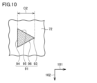
- FIG. 10 is a schematic bottom view showing the configuration of a triangular defect.
- FIG. 11 is a schematic cross-sectional view showing a step of forming a silicon carbide epitaxial layer on the second silicon carbide substrate.
- FIG. 12 is a schematic cross-sectional view showing a step of removing the fourth silicon carbide epitaxial layer by polishing.
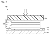
- FIG. 13 is a schematic cross-sectional view showing the configuration of a mechanical polishing apparatus.
- FIG. 14 is a flow diagram illustrating a schematic method for manufacturing a silicon carbide semiconductor device according to this embodiment.
- FIG. 15 is a schematic cross-sectional view showing a step of preparing a silicon carbide epitaxial substrate.
- FIG. 16 is a schematic cross-sectional view showing a step of forming a body region.
- FIG. 17 is a schematic cross-sectional view showing a step of forming a source region.
- FIG. 18 is a schematic cross-sectional view showing a step of forming a trench in the first main surface of the silicon carbide epitaxial layer.
- FIG. 19 is a schematic cross-sectional view showing a step of forming a gate insulating film.
- FIG. 15 is a schematic cross-sectional view showing a step of preparing a silicon carbide epitaxial substrate.
- FIG. 16 is a schematic cross-sectional view showing a step of forming a body region.
- FIG. 17 is a schematic cross-sectional view showing a step
- FIG. 20 is a schematic cross-sectional view showing a step of forming a gate electrode and an interlayer insulating film.
- FIG. 21 is a schematic cross-sectional view showing the configuration of a silicon carbide semiconductor device according to this embodiment.
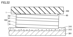
- FIG. 22 is a schematic cross-sectional view showing a state in which the protrusion is in contact with the polishing head.
- FIG. 23 is a schematic diagram showing measurement results of the LTV of each of a plurality of square regions after the step of forming a silicon carbide epitaxial layer on the second silicon carbide substrate and before the step of removing the fourth silicon carbide epitaxial layer by polishing.
- FIG. 24 is a schematic diagram showing the measurement results of the LTV of each of the plurality of square regions after the step of removing the fourth silicon carbide epitaxial layer by polishing.
- An object of the present disclosure is to provide a silicon carbide epitaxial substrate, a method for manufacturing a silicon carbide epitaxial substrate, and a method for manufacturing a silicon carbide semiconductor device, which are capable of improving the yield of silicon carbide semiconductor devices.
- the present disclosure can provide a silicon carbide epitaxial substrate capable of improving the yield of silicon carbide semiconductor devices, a method for manufacturing a silicon carbide epitaxial substrate, and a silicon carbide semiconductor device.
- a silicon carbide epitaxial substrate comprises a silicon carbide substrate and a silicon carbide epitaxial layer.
- the silicon carbide epitaxial layer is provided on the silicon carbide substrate.
- the silicon carbide epitaxial layer has a first main surface.
- the first main surface is opposite to the interface between the silicon carbide substrate and the silicon carbide epitaxial layer.
- On the first main surface there is a protrusion made of silicon carbide.
- the first main surface is made up of an outer edge, a peripheral region, and a central region.
- the peripheral region is a region within 3 mm from the outer edge.
- the central region is surrounded by the peripheral region.
- the plurality of square regions are made up of a first square region closest to the protrusion and second square regions which are a plurality of square regions other than the first square region.
- the LTV of the first square region is greater than the LTV of each of the multiple square regions that make up the second square region.
- the LTV of the first square region is 2 ⁇ m or less.
- the LTV of the first square region may be 1.5 ⁇ m or less.
- the thickness of the silicon carbide epitaxial layer may be 10 ⁇ m or more and 30 ⁇ m or less.
- the silicon carbide epitaxial substrate according to the present disclosure has a silicon carbide substrate and a silicon carbide epitaxial layer.
- the silicon carbide epitaxial layer is provided on the silicon carbide substrate.
- the silicon carbide epitaxial layer has a first main surface.
- the first main surface is opposite the interface between the silicon carbide substrate and the silicon carbide epitaxial layer.
- the silicon carbide substrate has a second main surface.
- the second main surface is opposite the interface.
- the first main surface is composed of an outer edge, a peripheral region, and a central region.
- the peripheral region is a region within 3 mm from the outer edge.
- the central region is surrounded by the outer edge region. When the central region is divided into a plurality of square regions with a side length of 10 mm, the maximum LTV value in the plurality of square regions is 2 ⁇ m or less.
- the maximum LTV value in the multiple square regions may be 1.5 ⁇ m or less.
- a method for manufacturing a silicon carbide epitaxial substrate includes the steps of preparing a first silicon carbide substrate having a first back surface and a first front surface opposite the first back surface, attaching silicon carbide particles to the first back surface, and forming a first silicon carbide epitaxial layer in contact with the first front surface and forming a second silicon carbide epitaxial layer in contact with the first back surface and the silicon carbide particles.
- steps of forming the first silicon carbide epitaxial layer and the second silicon carbide epitaxial layer triangular defects are formed in the second silicon carbide epitaxial layer starting from the silicon carbide particles.
- the method for manufacturing a silicon carbide epitaxial substrate according to the present disclosure further includes a step of measuring the thickness of the second silicon carbide epitaxial layer using triangular defects in the second silicon carbide epitaxial layer, a step of determining a polishing amount based on the measured thickness of the second silicon carbide epitaxial layer, a step of preparing a second silicon carbide substrate having a second back surface and a second front surface opposite the second back surface, a step of forming a third silicon carbide epitaxial layer in contact with the second front surface and a fourth silicon carbide epitaxial layer in contact with the second back surface, and a step of removing the fourth silicon carbide epitaxial layer by polishing based on the polishing amount.
- the thickness of the second silicon carbide epitaxial layer may be less than 1 ⁇ m.
- the amount of polishing may be 8.5 ⁇ m or more and 12.5 ⁇ m or less.
- the thickness of the second silicon carbide epitaxial layer may be 1 ⁇ m or more and 2 ⁇ m or less.
- the amount of polishing may be 11 ⁇ m or more and 16.5 ⁇ m or less.
- the method for manufacturing a silicon carbide semiconductor device includes the following steps: A silicon carbide epitaxial substrate according to any one of (1) to (5) above is prepared. An electrode is formed on the silicon carbide epitaxial layer.
- FIG. 1 is a schematic plan view showing the configuration of the silicon carbide substrate according to this embodiment.
- FIG. 2 is a schematic cross-sectional view taken along line II-II in FIG. 1.
- the silicon carbide epitaxial substrate 100 mainly has a first main surface 1, a second main surface 2, and an outer peripheral side surface 9.
- the second main surface 2 is opposite the first main surface 1.
- the outer peripheral side surface 9 is continuous with each of the first main surface 1 and the second main surface 2.
- the first main surface 1 is continuous with the outer peripheral side surface 9 at the outer edge 6.
- the first main surface 1 is composed of an outer edge 6, an outer peripheral region 11, and a central region 12.
- the outer peripheral region 11 is a region within 3 mm from the outer edge 6.
- the distance E between the outer edge 6 and the boundary between the outer peripheral region 11 and the central region 12 is 3 mm.
- the width (distance E) of the outer peripheral region 11 in the direction extending radially from the center O of the first main surface 1 (radial direction) is 3 mm.
- the central region 12 is surrounded by the peripheral region 11.
- the central region 12 is continuous with the peripheral region 11.
- the central region 12 is a region whose distance from the outer edge 6 is greater than 3 mm.
- the silicon carbide epitaxial substrate 100 is made of, for example, hexagonal silicon carbide.
- the polytype of the hexagonal silicon carbide is, for example, 4H.
- the outer peripheral side surface 9 has, for example, an orientation flat portion 7 and an arc-shaped portion 8.
- the orientation flat portion 7 when viewed along a straight line perpendicular to the first main surface 1, the orientation flat portion 7 is linear. When viewed along a straight line perpendicular to the first main surface 1, the orientation flat portion 7 may extend along the first direction 101.
- the arc-shaped portion 8 is continuous with the orientation flat portion 7. When viewed along a straight line perpendicular to the first main surface 1, the arc-shaped portion 8 is arc-shaped.
- the center O of the first main surface 1 is the center of a circle that includes an arc along the arc-shaped portion 8.
- the first principal surface 1 when viewed along a straight line perpendicular to the first principal surface 1, the first principal surface 1 extends along each of a first direction 101 and a second direction 102.
- the second direction 102 is a direction perpendicular to the first direction 101.
- the first direction 101 is, for example, the ⁇ 11-20> direction.
- the first direction 101 may be, for example, the [11-20] direction.
- the first direction 101 may be a direction obtained by projecting the ⁇ 11-20> direction onto the first principal surface 1. From another perspective, the first direction 101 may be, for example, a direction that includes a ⁇ 11-20> directional component.
- the second direction 102 is, for example, the ⁇ 1-100> direction.
- the second direction 102 may be, for example, the [1-100] direction.
- the second direction 102 may be, for example, a direction obtained by projecting the ⁇ 1-100> direction onto the first principal surface 1. From another perspective, the second direction 102 may be, for example, a direction that includes a ⁇ 1-100> directional component.
- the maximum diameter W of the first main surface 1 is not particularly limited, but is, for example, 100 mm (4 inches) or more.
- the maximum diameter W may be 125 mm (5 inches) or more, 150 mm (6 inches) or more, or 200 mm (8 inches) or more.
- the maximum diameter W may be, for example, 400 mm (16 inches) or less.
- the maximum diameter W is the longest straight distance between two different points on the outer edge 6.
- 4 inches means 100 mm or 101.6 mm (4 inches x 25.4 mm/inch). 6 inches means 150 mm or 152.4 mm (6 inches x 25.4 mm/inch). 8 inches means 200 mm or 203.2 mm (8 inches x 25.4 mm/inch). 16 inches means 400 mm or 406.4 mm (16 inches x 25.4 mm/inch).
- the third direction 103 is a direction from the second main surface 2 toward the first main surface 1.
- the third direction 103 is perpendicular to both the first direction 101 and the second direction 102.
- the cross section shown in FIG. 2 is perpendicular to the first main surface 1 and parallel to the first direction 101.
- the silicon carbide epitaxial substrate 100 has a silicon carbide substrate 30 and a silicon carbide epitaxial layer 40.
- the silicon carbide substrate 30 has a second main surface 2 and a third main surface 3.
- the second main surface 2 is the back surface of the silicon carbide epitaxial substrate 100.
- the second main surface 2 is opposite to the interface 5 between the silicon carbide substrate 30 and the silicon carbide epitaxial layer 40.
- the second main surface 2 is a polished surface.
- scratches (not shown) are formed on the second main surface 2.
- the scratches are damage formed during mechanical polishing and chemical mechanical polishing.
- the shape of the scratches is, for example, linear.
- the value obtained by dividing the length of the scratch in the longitudinal direction of the scratch by the length of the scratch in the lateral direction of the scratch may be, for example, 7 or more, 10 or more, or 15 or more.
- the second main surface 2 may not have triangular defects formed. The detailed configuration of the triangular defects will be described later.
- the third main surface 3 is opposite to the second main surface 2.
- the silicon carbide substrate 30 is in contact with the silicon carbide epitaxial layer 40.
- the silicon carbide substrate 30 contains an n-type impurity such as nitrogen.
- the conductivity type of the silicon carbide substrate 30 is, for example, n-type.
- the polytype of the silicon carbide constituting the silicon carbide substrate 30 is, for example, 4H.
- the thickness (second thickness H2) of the silicon carbide substrate 30 is, for example, 200 ⁇ m or more and 600 ⁇ m or less.
- the second thickness H2 is not particularly limited.
- the second thickness H2 may be, for example, 500 ⁇ m or less, or 350 ⁇ m or less.
- the silicon carbide epitaxial layer 40 is provided on the silicon carbide substrate 30.
- the silicon carbide epitaxial layer 40 has a first main surface 1.
- the first main surface 1 is the surface of the silicon carbide epitaxial substrate 100.
- the first main surface 1 is opposite the interface 5.
- the thickness (first thickness H1) of the silicon carbide epitaxial layer 40 is, for example, 10 ⁇ m or more and 30 ⁇ m or less.
- the first thickness H1 may be, for example, 13 ⁇ m or more, or 18 ⁇ m or more.
- the first thickness H1 may be, for example, 27 ⁇ m or less, or 22 ⁇ m or less.
- the first thickness H1 can be measured, for example, by using an FTIR (Fourier Transform InfraRed spectrometer).
- the measuring device is, for example, a Fourier transform infrared spectrophotometer (IRPrestige-21) manufactured by Shimadzu Corporation.
- the thickness of the silicon carbide layer epitaxial layer is measured by FTIR using an optical constant difference caused by a carrier concentration difference between the silicon carbide epitaxial layer 40 and the silicon carbide substrate 30.
- the measurement wave number range is, for example, from 3400 cm ⁇ 1 to 2400 cm ⁇ 1 .
- the wave number interval is, for example, about 4 cm ⁇ 1 .
- the silicon carbide epitaxial layer 40 has a buffer layer 41 and a drift layer 42.
- the drift layer 42 may be a single layer or may be two or more layers.
- the polytype of silicon carbide constituting the silicon carbide epitaxial layer 40 is, for example, 4H.
- the buffer layer 41 is provided on the silicon carbide substrate 30.
- the buffer layer 41 is in contact with the silicon carbide substrate 30.
- the buffer layer 41 contains an n-type impurity such as nitrogen.
- the conductivity type of the buffer layer 41 is, for example, n-type.
- the thickness of the buffer layer 41 in the third direction 103 is, for example, 1 ⁇ m or more.
- the drift layer 42 is provided on the buffer layer 41.
- the drift layer 42 is in contact with the buffer layer 41.
- the drift layer 42 constitutes the first main surface 1.
- the drift layer 42 contains n-type impurities such as nitrogen.
- the conductivity type of the drift layer 42 is, for example, n-type.
- the concentration of the n-type impurities in the drift layer 42 is, for example, smaller than the concentration of the n-type impurities in the buffer layer 41.
- the thickness of the drift layer 42 in the third direction 103 is, for example, 10 ⁇ m or more.
- the first main surface 1 is a surface inclined with respect to the ⁇ 0001 ⁇ surface.
- the off angle ⁇ of the first main surface 1 with respect to the ⁇ 0001 ⁇ surface is, for example, greater than 0° and equal to or less than 8°.
- the first main surface 1 may be a surface inclined by the off angle ⁇ with respect to the (0001) surface.
- the first main surface 1 may be a surface inclined by the off angle ⁇ with respect to the (000-1) surface.
- the inclination direction (off direction) of the first main surface 1 with respect to the ⁇ 0001 ⁇ surface is, for example, the ⁇ 11-20> direction.
- the off angle ⁇ is not particularly limited.
- the off angle ⁇ may be, for example, 7° or less, 6° or less, or 5° or less.
- the off angle ⁇ may be, for example, 1° or more, or 2° or more.
- FIG. 3 is an enlarged schematic cross-sectional view taken along line III-III in FIG. 1.
- the cross section shown in FIG. 3 is parallel to both the third direction 103 and the radial direction.
- a protrusion 60 is present on the first main surface 1.
- the protrusion 60 is located, for example, in the outer peripheral region 11.
- the protrusion 60 may also be located in the central region 12.
- the protrusion 60 is shown using a black circle in FIG. 1.
- the protrusion 60 is convex along the third direction 103.
- a portion of the protrusion 60 may be located radially outward from the outer peripheral side surface 9.
- the protrusion 60 may cover a portion of the outer edge 6 (see FIG. 1).
- the protrusion 60 is made of silicon carbide.
- the protrusion 60 is, for example, an epicrown or a particle.
- the shape of the protrusion 60 is, for example, circular.
- the width of the protrusion 60 in the radial direction is a first width F1.
- the protrusion 60 forms a convex surface 66.
- the convex surface 66 is convex along the third direction 103.
- the convex surface 66 forms a part of the first main surface 1.
- the convex surface 66 may be connected to the outer peripheral side surface 9.
- the first main surface 1 has a first flat surface 81 and a second flat surface 82.
- the first flat surface 81 is connected to the convex surface 66.
- the first flat surface 81 extends along both the first direction 101 and the second direction 102.
- the second flat surface 82 is continuous with the first flat surface 81.
- the second flat surface 82 is spaced apart from the convex surface 66.
- the first flat surface 81 is provided between the second flat surface 82 and the protrusion 60.
- the vertex 61 is the vertex of the protrusion 60.
- the height D1 of the protrusion 60 is, for example, 5 ⁇ m or more, and there is no particular upper limit to the height D1.
- the height D1 is the distance between the vertex 61 and the first flat surface 81 and the second flat surface 82 in the third direction 103.
- the second principal surface 2 has a concave surface 69 and a third flat surface 83.
- the concave surface 69 is opposite the protrusion 60.
- the concave surface 69 is opposite the first flat surface 81.
- the first flat surface 81 is a portion of the first principal surface 1 opposite the concave surface 69.
- An imaginary straight line 99 that passes through the vertex 61 and extends along the third direction 103 passes through the concave surface 69.
- the concave surface 69 surrounds the imaginary straight line 99.
- the concave surface 69 is inclined in the third direction 103 with respect to the radial direction.
- the concave surface 69 forms a recess 67.
- the depth D2 of the concave surface 69 in the third direction 103 may be greater than the height D1 of the protrusion 60.
- the width of the concave surface 69 in the radial direction is a second width F2.
- the second width F2 is greater than the first width F1.
- the value obtained by dividing the second width F2 by the first width F1 is, for example, 10 or more and 1000 or less.
- the second width F2 is, for example, 5 mm.
- the second width F2 may be, for example, 1 mm or more and 20 mm or less.
- the third flat surface 83 is continuous with the concave surface 69.
- the third flat surface 83 extends along each of the first direction 101 and the second direction 102.
- the third flat surface 83 is opposite the second flat surface 82.
- the second flat surface 82 is a portion of the first main surface 1 opposite the third flat surface 83.
- the concave surface 69 is inclined in the third direction 103 relative to the third flat surface 83. In a cross section perpendicular to the radial direction and parallel to the third direction 103, the concave surface 69 is concave along the third direction 103.
- LTV local thickness variation
- FIG. 4 is a schematic plan view showing the measurement area of the LTV.
- the protrusions 60 are shown as black circles.
- the central region 12 of the silicon carbide epitaxial substrate 100 is divided into a plurality of square regions 50.
- the shape of each of the plurality of square regions 50 is substantially a square.
- the length of one side of each of the plurality of square regions 50 is set to a first length C1.
- the first length C1 is 10 mm.
- the maximum diameter W (see FIG. 1) of the first main surface 1 is, for example, 150 mm.
- a 150 mm x 150 mm square circumscribing the outer peripheral side surface 9 is assumed.
- the number of square regions 50 inside the central region 12 is, for example, 141.
- the square regions that intersect with the boundary between the peripheral region 11 and the central region 12 are missing parts and are not complete square regions. Therefore, the square regions that intersect with the boundary between the peripheral region 11 and the central region 12 are not considered to be square regions 50 that make up the central region 12.
- one side of each of the multiple square regions 50 is parallel to the extension direction of the orientation flat portion 7. The LTV is measured in each of the multiple square regions 50.
- the multiple square regions 50 are composed of a first square region 51 and multiple second square regions 52.
- the first square region 51 is the square region 50 closest to the protrusion 60.
- the square region 50 closest to the vertex 61 (see FIG. 3) of the protrusion 60 when viewed along a straight line perpendicular to the first main surface 1 is determined to be the first square region 51.
- the square region 50 in which the vertex 61 is located is determined to be the first square region 51. Note that when there are multiple protrusions on the first main surface 1, the protrusion with the highest height D1 is identified as the above-mentioned protrusion 60.
- the first square region 51 may include at least a portion of the first flat surface 81 (see FIG. 3).
- the first square region 51 may include at least a portion of the convex surface 66 (see FIG. 3). In FIG. 4, the shaded region indicates the first square region 51.
- the second square regions 52 are square regions 50 other than the first square region 51.
- the number of the second square regions 52 is, for example, 140.
- the second square regions 52 are connected to the first square region 51.
- Figure 5 is a schematic diagram explaining the definition of LTV.
- LTV
- the LTV is measured, for example, by the following procedure. First, silicon carbide epitaxial substrate 100 is prepared. Either first main surface 1 or second main surface 2 is set as an adsorption surface B that is adsorbed to a flat chuck surface. The surface opposite to adsorption surface B is set as measurement surface A.
- the suction surface B is entirely attached to the chuck surface.
- an image of the measurement surface A on the opposite side of the suction surface B is optically acquired.
- the LTV is the value obtained by subtracting the height from the suction surface B to the lowest point P2 of the measurement surface A (minimum height T2) from the height from the suction surface B to the highest point P1 of the measurement surface A (maximum height T1) when the suction surface B is entirely attached to the flat chuck surface.
- the LTV is the value obtained by subtracting the shortest distance between the measurement surface A and the suction surface B from the longest distance between the measurement surface A and the suction surface B in the direction perpendicular to the suction surface B.
- the LTV is the distance between the plane (first plane L1) that passes through the highest point P1 and is parallel to the suction surface B, and the plane (second plane L2) that passes through the lowest point P2 and is parallel to the suction surface B.
- the maximum value of the LTV in the multiple square regions 50 is 2 ⁇ m or less.
- the maximum value of the LTV in the multiple square regions 50 may be, for example, 1.5 ⁇ m or less, 1.3 ⁇ m or less, or 1.1 ⁇ m or less.
- the maximum value of the LTV in the multiple square regions 50 may be, for example, 0.1 ⁇ m or more, or 0.5 ⁇ m or more.
- the LTV of the first square region 51 is 2 ⁇ m or less.
- the LTV of the first square region 51 may be, for example, 1.5 ⁇ m or less, 1.3 ⁇ m or less, or 1.1 ⁇ m or less.
- the LTV of the first square region 51 may be, for example, 0.1 ⁇ m or more, or 0.5 ⁇ m or more.
- the LTV of each of the second square regions 52 is, for example, 0.1 ⁇ m or more and 1.0 ⁇ m or less.
- the LTV of the first square region 51 is greater than the LTV of each of the second square regions 52. From another perspective, among the multiple square regions 50, the first square region 51 is the square region 50 with the largest LTV.
- Fig. 6 is a partial cross-sectional schematic diagram showing the configuration of the manufacturing apparatus for silicon carbide epitaxial substrate 100.
- the manufacturing apparatus 200 for silicon carbide epitaxial substrate 100 is, for example, a hot-wall type horizontal CVD (Chemical Vapor Deposition) apparatus.
- the manufacturing apparatus 200 for silicon carbide epitaxial substrate 100 mainly includes a reaction chamber 201, a gas supply unit 235, a control unit 245, a heating element 203, a quartz tube 204, a heat insulating material (not shown), and an induction heating coil (not shown).
- the heating element 203 has, for example, a cylindrical shape, and forms a reaction chamber 201 inside.
- the heating element 203 is made of, for example, graphite.
- the heating element 203 is provided inside a quartz tube 204.
- a heat insulating material surrounds the outer periphery of the heating element 203.
- the induction heating coil is wound, for example, along the outer periphery of the quartz tube 204.
- the induction heating coil is configured so that an alternating current can be supplied to it by an external power source (not shown). This causes the heating element 203 to be induction heated. As a result, the reaction chamber 201 is heated by the heating element 203.
- the reaction chamber 201 is a space surrounded by the inner wall surface 205 of the heating element 203.
- a susceptor 210 that holds a silicon carbide substrate 30 is provided in the reaction chamber 201.
- the susceptor 210 is made of silicon carbide.
- the silicon carbide substrate 30 is placed on the susceptor 210.
- the susceptor 210 is placed on a stage 202.
- the stage 202 is supported by a rotating shaft 209 so that it can rotate on its own axis. The rotation of the stage 202 causes the susceptor 210 to rotate.
- the manufacturing apparatus 200 for the silicon carbide epitaxial substrate 100 further has a gas inlet 207 and a gas exhaust port 208.
- the gas exhaust port 208 is connected to an exhaust pump (not shown).
- the arrows in FIG. 6 indicate the flow of gas. Gas is introduced into the reaction chamber 201 from the gas inlet 207 and exhausted from the gas exhaust port 208.
- the pressure inside the reaction chamber 201 is adjusted by balancing the amount of gas supplied and the amount of gas exhausted.
- the gas supply unit 235 is configured to be able to supply a mixed gas containing a raw material gas, a dopant gas, and a carrier gas to the reaction chamber 201.
- the gas supply unit 235 includes, for example, a first gas supply unit 231, a second gas supply unit 232, a third gas supply unit 233, and a fourth gas supply unit 234.
- the first gas supply unit 231 is configured to be able to supply a first gas containing, for example, carbon (C) atoms.
- the first gas supply unit 231 is, for example, a gas cylinder filled with the first gas.
- the first gas is, for example, propane ( C3H8 ) gas.
- the first gas may be, for example, methane ( CH4 ) gas , ethane ( C2H6 ) gas, acetylene ( C2H2 ) gas, or the like.
- the second gas supply unit 232 is configured to be able to supply a second gas including, for example, silane (SiH 4 ) gas.
- the second gas supply unit 232 is, for example, a gas cylinder filled with the second gas.
- the second gas is, for example, silane gas.
- the second gas may be a mixed gas of silane gas and a gas other than silane.
- the third gas supply unit 233 is configured to be able to supply a third gas containing, for example, nitrogen atoms.
- the third gas supply unit 233 is, for example, a gas cylinder filled with the third gas.
- the third gas is a doping gas.
- the third gas is, for example, ammonia gas. Ammonia gas is more susceptible to thermal decomposition than nitrogen gas, which has a triple bond.
- the fourth gas supply unit 234 is configured to be capable of supplying a fourth gas (carrier gas) such as hydrogen.
- the fourth gas supply unit 234 is, for example, a gas cylinder filled with hydrogen.
- the fourth gas supply unit 234 may also be, for example, a gas cylinder filled with argon.
- the control unit 245 is configured to be able to control the flow rate of the mixed gas supplied from the gas supply unit 235 to the reaction chamber 201.
- the control unit 245 may include a first gas flow rate control unit 241, a second gas flow rate control unit 242, a third gas flow rate control unit 243, and a fourth gas flow rate control unit 244.
- Each control unit may be, for example, an MFC (Mass Flow Controller).
- the control unit 245 is disposed between the gas supply unit 235 and the gas inlet 207.
- FIG. 7 is a flow diagram that outlines the method for manufacturing the silicon carbide epitaxial substrate 100 according to this embodiment. As shown in FIG.
- the method for manufacturing the silicon carbide epitaxial substrate 100 mainly includes a step of preparing a first silicon carbide substrate (S10), a step of attaching silicon carbide particles to the first back surface (S20), a step of forming a silicon carbide epitaxial layer on the first silicon carbide substrate (S30), a step of measuring the thickness of the second silicon carbide epitaxial layer (S40), a step of determining the amount of polishing (S50), a step of preparing a second silicon carbide substrate (S60), a step of forming a silicon carbide epitaxial layer on the second silicon carbide substrate (S70), and a step of removing the fourth silicon carbide epitaxial layer by polishing (S80).
- a step (S10) of preparing a first silicon carbide substrate is performed. Specifically, an ingot made of silicon carbide single crystal produced by, for example, sublimation is sliced with a wire saw to prepare a plurality of silicon carbide substrates 30. Each of the plurality of silicon carbide substrates 30 has a diameter of, for example, 100 mm or more.
- the thickness (second thickness H2) of the silicon carbide substrate 30 is, for example, 200 ⁇ m or more and 600 ⁇ m or less.
- one silicon carbide substrate 30 is prepared as a first silicon carbide substrate 31.
- the first silicon carbide substrate 31 is a dummy silicon carbide substrate 30.
- the first silicon carbide substrate 31 is a silicon carbide substrate 30 that is different from a second silicon carbide substrate 32 described later.
- FIG. 8 is a schematic cross-sectional view showing the step (S20) of adhering silicon carbide particles to the first back surface.
- the first silicon carbide substrate 31 has a first back surface 62 and a first front surface 63.
- the first surface 63 is opposite the first back surface 62.
- silicon carbide particles 90 are attached to the first back surface 62. Specifically, the silicon carbide particles 90 are attached to the second main surface 2 using, for example, tweezers. The silicon carbide particles 90 have a diameter of, for example, about 20 ⁇ m. The silicon carbide particles 90 are attached, for example, near the center of the second main surface 2.
- FIG. 9 is a cross-sectional schematic diagram showing the step (S30) of forming a silicon carbide epitaxial layer on the first silicon carbide substrate.
- the first silicon carbide substrate 31 is placed on the susceptor 210 of the manufacturing apparatus 200 (see FIG. 6) of the silicon carbide epitaxial substrate 100. Specifically, the first silicon carbide substrate 31 is placed on the susceptor 210 so that the first back surface 62 is in contact with the susceptor 210.
- the reaction chamber 201 is depressurized. Specifically, the pressure in the reaction chamber 201 is reduced from atmospheric pressure to, for example, about 1 ⁇ 10 ⁇ 6 Pa.
- the temperature rise of the first silicon carbide substrate 31 is started. During the temperature rise, hydrogen (H 2 ) gas, which is a carrier gas, is introduced into the reaction chamber 201 from the fourth gas supply unit 234.
- hydrogen (H 2 ) gas which is a carrier gas
- a buffer layer 41 is formed on the first surface 63.
- a raw material gas, a dopant gas, and a carrier gas are supplied to the reaction chamber 201. More specifically, a mixed gas containing, for example, silane, propane, ammonia, and hydrogen is introduced into the reaction chamber 201. In the reaction chamber 201, each gas is thermally decomposed.
- the flow rate of the first gas is, for example, 29 sccm.
- the flow rate of the second gas is, for example, 46 sccm.
- the flow rate of the third gas is, for example, 1.5 sccm.
- the flow rate of the fourth gas is, for example, 100 slm.
- the pressure inside the reaction chamber 201 is maintained, for example, at least 2 kPa and not more than 6 kPa.
- the growth temperature is, for example, at least 1500°C and not more than 1700°C.
- the buffer layer 41 is formed on the first surface 63 as shown in FIG. 9.
- the thickness of the buffer layer 41 is, for example, 5 ⁇ m or more.
- the drift layer 42 is formed on the buffer layer 41.
- the flow rate of the first gas is, for example, 29 sccm.
- the flow rate of the second gas is, for example, 46 sccm.
- the flow rate of the third gas is, for example, 1.5 sccm.
- the flow rate of the fourth gas is, for example, 100 slm.
- the growth temperature is, for example, 1500°C or higher and 1700°C or lower.
- the buffer layer 41 and the drift layer 42 constitute the first silicon carbide epitaxial layer 71.
- the first silicon carbide epitaxial layer 71 in contact with the first surface 63 is formed.
- the step flow growth direction (off-direction of the first main surface 1) of the first silicon carbide epitaxial layer 71 is, for example, the first direction 101.
- the configuration of the first silicon carbide epitaxial layer 71 is substantially the same as the configuration of the silicon carbide epitaxial layer 40.
- a step of forming a buffer layer 41 on the first surface 63 and a step of forming a drift layer 42 on the buffer layer 41 are performed to form a second silicon carbide epitaxial layer 72 in contact with the first back surface 62 and the silicon carbide particles 90.
- the second silicon carbide epitaxial layer 72 is formed, for example, by sublimation of a portion of a silicon carbide susceptor 210 (see FIG. 6) and deposition on the second main surface 2 of the silicon carbide substrate 30.
- the step flow growth direction of the second silicon carbide epitaxial layer 72 is, for example, the direction opposite to the first direction 101.
- the thickness of the second silicon carbide epitaxial layer 72 in the third direction 103 is a third thickness H3.
- the second silicon carbide epitaxial layer 72 has a triangular defect 91.
- the triangular defect 91 is formed starting from a silicon carbide particle 90.
- the polytype of silicon carbide constituting the triangular defect 91 is, for example, 3C.
- the triangular defect 91 has a bottom surface portion 92.
- the bottom surface portion 92 is connected to the silicon carbide particle 90.
- the bottom surface portion 92 is located on the basal plane.
- the bottom surface portion 92 is inclined relative to the first back surface 62 in the direction opposite to the third direction 103.
- the inclination angle of the first back surface 62 relative to the bottom surface portion 92 is the off angle ⁇ .
- the triangular defect 91 has a first side portion 95, a second side portion 96, and a bottom portion 94.
- the second side portion 96 is connected to the first side portion 95.
- the boundary between the second side portion 96 and the first side portion 95 is an end point 93.
- the first side portion 95 and the second side portion 96 branch into two from the end point 93.
- the bottom portion 94 is in the opposite direction to the first direction 101 with respect to the end point 93.
- the bottom portion 94 is connected to each of the first side portion 95 and the second side portion 96.
- the first side portion 95 is connected to one end (first end portion) of the bottom portion 94
- the second side portion 96 is connected to the other end (second end portion) of the base portion 94.
- the first side portion 95 When viewed along the third direction 103, the first side portion 95 is inclined with respect to each of the first direction 101 and the second direction 102.
- the first side portion 95 may be inclined from a straight line parallel to the first direction 101 toward the second direction 102.
- the second side portion 96 may be inclined from a straight line parallel to the first direction 101 in a direction opposite to the second direction 102.
- the base portion 94 When viewed along the third direction 103, the base portion 94 extends along the second direction 102.
- the width of the triangular defect 91 in the second direction 102 may increase from the end point 93 toward the base portion 94.
- the length of the triangular defect 91 in the step flow growth direction of the second silicon carbide epitaxial layer 72 (the direction opposite to the first direction 101) is defined as a second length C2.
- the second length C2 is the maximum distance between the end point 93 and the base portion 94 in the first direction 101.
- a step (S40) of measuring the thickness of the second silicon carbide epitaxial layer is performed. Specifically, first, the second length C2 is measured. In measuring the second length C2, for example, a confocal scanning device is used. As the confocal scanning device, for example, the WASAVI series "SICA 6X" manufactured by Lasertec Corporation can be used. The magnification of the objective lens is, for example, 10 times. Based on the measured second length C2, the third thickness H3 is calculated using Equation 2. As described above, the thickness (third thickness H3) of the second silicon carbide epitaxial layer 72 is measured using the triangular defect 91.
- the thickness of the fourth silicon carbide epitaxial layer 74 is thinner than the thickness of the silicon carbide epitaxial layer 40. Therefore, it is difficult to measure the thickness of the fourth silicon carbide epitaxial layer 74 using a measurement method such as FTIR (Fourier Transform InfraRed spectrometer).
- FTIR Fastier Transform InfraRed spectrometer
- the step of determining the amount of polishing (S50) is performed.
- the amount of back surface polishing H4 is determined based on the third thickness H3 measured in the step of measuring the thickness of the second silicon carbide epitaxial layer (S40).
- the amount of back surface polishing H4 is the amount by which the fourth silicon carbide epitaxial layer 74 and the second silicon carbide substrate 32 are polished in the step of removing the fourth silicon carbide epitaxial layer (S80) described below.
- the third thickness H3 may be, for example, less than 1 ⁇ m.
- the back surface grinding amount H4 is, for example, 9 ⁇ m.
- the back surface grinding amount H4 may be, for example, 8.5 ⁇ m or more and 12.5 ⁇ m or less.
- the back surface grinding amount H4 may be, for example, 9 ⁇ m or more, or 9.5 ⁇ m or more.
- the back surface grinding amount H4 may be, for example, 11 ⁇ m or less, or 10 ⁇ m or less.
- the third thickness H3 may be, for example, 1 ⁇ m or more and 2 ⁇ m or less.
- the back surface grinding amount H4 may be, for example, 13.5 ⁇ m.
- the back surface grinding amount H4 may be, for example, 11 ⁇ m or more and 16.5 ⁇ m or less.
- the back surface grinding amount H4 may be, for example, 11.5 ⁇ m or more, or 12 ⁇ m or more.
- the back surface grinding amount H4 may be, for example, 15 ⁇ m or less, or 14 ⁇ m or more.
- the step of preparing a second silicon carbide substrate (S60) is performed. Specifically, one of the multiple silicon carbide substrates 30 produced in the step of preparing a first silicon carbide substrate (S10) is prepared as the second silicon carbide substrate 32.
- the configuration of the second silicon carbide substrate 32 is substantially the same as the configuration of the first silicon carbide substrate 31.
- the second silicon carbide substrate 32 is epitaxially grown under the same growth conditions as the step of forming a silicon carbide epitaxial layer on the first silicon carbide substrate (S30), and may be a silicon carbide substrate 30 used for epitaxial growth of a different batch from the step of forming a silicon carbide epitaxial layer on the first silicon carbide substrate (S30).
- FIG. 11 is a schematic cross-sectional view showing the step (S70) of forming a silicon carbide epitaxial layer on the second silicon carbide substrate.
- the second silicon carbide substrate 32 has a second back surface 64 and a second front surface 65.
- the second surface 65 is opposite the second back surface 64.
- the second back surface 64 corresponds to the first back surface 62 (see FIG. 9).
- the second surface 65 corresponds to the first surface 63 (see FIG. 9).
- a third silicon carbide epitaxial layer 73 and a fourth silicon carbide epitaxial layer 74 are formed under substantially the same conditions as in the step (S30) of forming a silicon carbide epitaxial layer on the first silicon carbide substrate.
- a third silicon carbide epitaxial layer 73 is formed in contact with the second surface 65.
- the third silicon carbide epitaxial layer 73 has a buffer layer 41 and a drift layer 42.
- the configuration of the third silicon carbide epitaxial layer 73 is substantially the same as the configuration of each of the silicon carbide epitaxial layer 40 (see FIG. 2) and the first silicon carbide epitaxial layer 71 (see FIG. 9).
- a fourth silicon carbide epitaxial layer 74 is formed in contact with the second back surface 64.
- the fourth silicon carbide epitaxial layer 74 corresponds to the second silicon carbide epitaxial layer 72 (see FIG. 9).
- the fourth silicon carbide epitaxial layer 74 may not have a triangular defect 91.
- the thickness of the fourth silicon carbide epitaxial layer 74 in the third direction 103 may be substantially the third thickness H3.
- FIG. 12 is a schematic cross-sectional view showing the step (S80) of removing the fourth silicon carbide epitaxial layer by polishing.
- the portion indicated by the dashed line in FIG. 12 shows the state of the silicon carbide epitaxial substrate 100 before polishing.
- the portion indicated by the solid line in FIG. 12 shows the state of the silicon carbide epitaxial substrate 100 after chemical mechanical polishing. As shown in FIG. 12, mechanical polishing is performed on the fourth silicon carbide epitaxial layer 74 and the second silicon carbide substrate 32.
- FIG. 13 is a schematic cross-sectional view showing the configuration of a mechanical polishing apparatus.
- the mechanical polishing apparatus 300 has a surface plate 301 and a polishing head 302.
- the silicon carbide epitaxial substrate 100 is attached to the polishing head 302.
- the first main surface 1 of the silicon carbide epitaxial substrate 100 contacts the polishing head 302.
- the fourth silicon carbide epitaxial layer 74 faces the surface plate 301.
- the polishing head 302 is, for example, ceramic or stainless steel.
- Slurry 310 is supplied between silicon carbide epitaxial substrate 100 and platen 301.
- Slurry 310 contains, for example, abrasive grains 312.
- Abrasive grains 312 are, for example, diamond or cubic boron nitride (cBN).
- the diameter of abrasive grains 312 is, for example, 1 ⁇ m or more and 3 ⁇ m or less.
- the platen 301 rotates.
- the polishing head 302 presses the silicon carbide epitaxial substrate 100 against the platen 301. This mechanically polishes the fourth silicon carbide epitaxial layer 74 and the second silicon carbide substrate 32. As a result, the fourth silicon carbide epitaxial layer 74 is removed.
- the amount of polishing in the mechanical polishing is, for example, 7 ⁇ m or more and 16.5 ⁇ m or less.
- silicon carbide epitaxial substrate 100 is positioned so that second back surface 64 faces a polishing cloth (not shown).
- a polishing liquid (not shown) is supplied between second back surface 64 and the polishing cloth.
- the polishing liquid contains, for example, abrasive grains and an oxidizer.
- the abrasive grains are, for example, colloidal silica, fumed silica, and alumina.
- the oxidizer is, for example, hydrogen peroxide.
- the polishing cloth rotates.
- the second back surface 64 is pressed against the polishing cloth. This causes the second silicon carbide substrate 32 to be chemically mechanically polished. As a result, the portion of the second silicon carbide substrate 32 that has been damaged by the mechanical polishing is removed.
- the amount of polishing in the chemical mechanical polishing is, for example, 0.05 ⁇ m or more and 1 ⁇ m or less.
- the back surface polishing amount H4 is the sum of the amount of the removed fourth silicon carbide epitaxial layer 74 and the amount of the removed second silicon carbide substrate 32.
- the thickness of the second silicon carbide substrate 32 in the third direction 103 is the second thickness H2.
- the silicon carbide epitaxial substrate 100 may be washed using a cleaning liquid such as pure water, acid, or alkali. In this manner, the silicon carbide epitaxial substrate 100 according to this embodiment is manufactured.
- the correspondence between the silicon carbide epitaxial substrate 100 shown in FIG. 12 and the silicon carbide epitaxial substrate 100 shown in FIG. 2 will be described.
- the second silicon carbide substrate 32 corresponds to the silicon carbide substrate 30.
- the third silicon carbide epitaxial layer 73 corresponds to the silicon carbide epitaxial layer 40.
- the second back surface 64 corresponds to the second main surface 2.
- the second front surface 65 corresponds to the third main surface 3.
- the step (S30) of forming a silicon carbide epitaxial layer on the first silicon carbide substrate is followed by the step (S70) of forming a silicon carbide epitaxial layer on the second silicon carbide substrate.
- epitaxial growth is performed on a batch separate from the step (S30) of forming a silicon carbide epitaxial layer on the first silicon carbide substrate.
- the configuration of the method for manufacturing the silicon carbide epitaxial substrate 100 according to the present disclosure is not limited to the above configuration.
- the step (S30) of forming a silicon carbide epitaxial layer on the first silicon carbide substrate and the step (S70) of forming a silicon carbide epitaxial layer on the second silicon carbide substrate may be performed by epitaxial growth of the same batch.
- the step (S60) of preparing the second silicon carbide substrate may be performed simultaneously with the step (S10) of preparing the first silicon carbide substrate.
- the step (S70) of forming a silicon carbide epitaxial layer on the second silicon carbide substrate may be performed simultaneously with the step (S30) of forming a silicon carbide epitaxial layer on the first silicon carbide substrate.
- Fig. 14 is a flow diagram that outlines the method for manufacturing the silicon carbide semiconductor device 400 according to this embodiment.
- the method for manufacturing the silicon carbide semiconductor device 400 according to this embodiment mainly includes a step (S1) of preparing the silicon carbide epitaxial substrate 100 and a step (S2) of processing the silicon carbide epitaxial substrate 100.
- FIG. 15 is a schematic cross-sectional view showing the step of preparing a silicon carbide epitaxial substrate 100.
- a silicon carbide epitaxial substrate 100 according to this embodiment is prepared (see FIGS. 1 and 2).
- a step (S2) of processing the silicon carbide epitaxial substrate 100 is carried out.
- the silicon carbide epitaxial substrate 100 is processed as follows. First, ions are implanted into the silicon carbide epitaxial substrate 100.
- FIG. 16 is a schematic cross-sectional view showing the process of forming a body region.
- p-type impurities such as aluminum are ion-implanted into the second main surface 2 of the silicon carbide epitaxial layer 40.
- This forms a body region 113 having p-type conductivity.
- the portion where the body region 113 is not formed becomes the drift layer 42 and the buffer layer 41.
- the thickness of the body region 113 is, for example, 0.9 ⁇ m.
- the silicon carbide epitaxial layer 40 includes the buffer layer 41, the drift layer 42, and the body region 113.
- FIG. 17 is a schematic cross-sectional view showing the step of forming a source region.
- n-type impurities such as phosphorus are ion-implanted into the body region 113.
- This forms a source region 114 having an n-type conductivity type.
- the thickness of the source region 114 is, for example, 0.4 ⁇ m.
- the concentration of the n-type impurities in the source region 114 is higher than the concentration of the p-type impurities in the body region 113.
- a p-type impurity such as aluminum is ion-implanted into the source region 114 to form a contact region 118.
- the contact region 118 is formed so as to penetrate the source region 114 and the body region 113 and contact the drift layer 42.
- the concentration of the p-type impurity in the contact region 118 is higher than the concentration of the n-type impurity in the source region 114.
- activation annealing is performed to activate the ion-implanted impurities.
- the temperature of the activation annealing is, for example, 1500°C or higher and 1900°C or lower.
- the activation annealing time is, for example, about 30 minutes.
- the atmosphere of the activation annealing is, for example, an argon atmosphere.
- FIG. 18 is a cross-sectional schematic diagram showing a step of forming a trench in the first main surface 1 of the silicon carbide epitaxial layer 40.
- a mask 117 having an opening is formed on the first main surface 1 including the source region 114 and the contact region 118.
- the source region 114, the body region 113, and a part of the drift layer 42 are removed by etching using the mask 117.
- etching method for example, inductively coupled plasma reactive ion etching can be used. Specifically, for example, inductively coupled plasma reactive ion etching using SF 6 or a mixed gas of SF 6 and O 2 as a reactive gas is used.
- a recess is formed in the first main surface 1 by etching.
- thermal etching is performed in the recess.
- the thermal etching can be performed, for example, by heating in an atmosphere containing a reactive gas having at least one or more types of halogen atoms, with the mask 117 formed on the first main surface 1.
- the at least one or more types of halogen atoms include at least one of chlorine (Cl) atoms and fluorine (F) atoms.
- the atmosphere includes, for example, Cl 2 , BCl 3 , SF 6 or CF 4.
- a mixed gas of chlorine gas and oxygen gas is used as the reactive gas, and the thermal etching is performed at a heat treatment temperature of, for example, 700° C. or more and 1000° C. or less.
- the reactive gas may include a carrier gas in addition to the above-mentioned chlorine gas and oxygen gas.
- nitrogen gas, argon gas, or helium gas can be used as the carrier gas.
- a trench 56 is formed in the first main surface 1 by thermal etching.
- the trench 56 is defined by a sidewall surface 53 and a bottom wall surface 54.
- the sidewall surface 53 is formed by the source region 114, the body region 113, and the drift layer 42.
- the bottom wall surface 54 is formed by the drift layer 42.
- the mask 117 is removed from the first main surface 1.
- FIG. 19 is a schematic cross-sectional view showing the step of forming a gate insulating film.
- silicon carbide epitaxial substrate 100 having trenches 56 formed in first main surface 1 is heated in an oxygen-containing atmosphere at a temperature of, for example, 1300° C. or higher and 1400° C. or lower.
- This forms gate insulating film 115 that contacts drift layer 42 at bottom wall surface 54, contacts drift layer 42, body region 113, and source region 114 at side wall surface 53, and contacts source region 114 and contact region 118 at first main surface 1.
- FIG. 20 is a schematic cross-sectional view showing the step of forming a gate electrode and an interlayer insulating film.
- Gate electrode 127 is formed inside trench 56 so as to contact gate insulating film 115.
- Gate electrode 127 is disposed inside trench 56 and formed on gate insulating film 115 so as to face each of sidewall surface 53 and bottom wall surface 54 of trench 56.
- Gate electrode 127 is formed, for example, by LPCVD (Low Pressure Chemical Vapor Deposition).
- the interlayer insulating film 126 is formed.
- the interlayer insulating film 126 is formed so as to cover the gate electrode 127 and to be in contact with the gate insulating film 115.
- the interlayer insulating film 126 is formed, for example, by chemical vapor deposition.
- the interlayer insulating film 126 is composed of a material containing, for example, silicon dioxide.
- a portion of the interlayer insulating film 126 and the gate insulating film 115 are etched so as to form openings over the source region 114 and the contact region 118. As a result, the contact region 118 and the source region 114 are exposed from the gate insulating film 115.
- the source electrode 116 is formed so as to contact each of the source region 114 and the contact region 118.
- the source electrode 116 is formed, for example, by a sputtering method.
- the source electrode 116 is made of a material containing, for example, Ti (titanium), Al (aluminum), and Si (silicon).
- alloying annealing is performed. Specifically, the source electrode 116 in contact with each of the source region 114 and the contact region 118 is held at a temperature of, for example, 900°C or higher and 1100°C or lower for about 5 minutes. As a result, at least a portion of the source electrode 116 is silicided. As a result, the source electrode 116 that forms an ohmic junction with the source region 114 is formed. The source electrode 116 may also form an ohmic junction with the contact region 118.
- the source wiring 119 is formed.
- the source wiring 119 is electrically connected to the source electrode 116.
- the source wiring 119 is formed so as to cover the source electrode 116 and the interlayer insulating film 126.
- a process for forming a drain electrode is carried out.
- the silicon carbide substrate 30 is polished at the second main surface 2. This reduces the thickness of the silicon carbide substrate 30.
- the drain electrode 123 is formed. The drain electrode 123 is formed so as to be in contact with the second main surface 2. In this manner, the silicon carbide semiconductor device 400 according to this embodiment is manufactured.
- FIG. 21 is a schematic cross-sectional view showing the configuration of a silicon carbide semiconductor device 400 according to this embodiment.
- the silicon carbide semiconductor device 400 is, for example, a MOSFET (Metal Oxide Semiconductor Field Effect Transistor).
- the silicon carbide semiconductor device 400 mainly includes a silicon carbide epitaxial substrate 100, a gate electrode 127, a gate insulating film 115, a source electrode 116, a drain electrode 123, a source wiring 119, and an interlayer insulating film 126.
- the silicon carbide epitaxial substrate 100 includes a buffer layer 41, a drift layer 42, a body region 113, a source region 114, and a contact region 118.
- the silicon carbide semiconductor device 400 may be, for example, an IGBT (Insulated Gate Bipolar Transistor).
- a part of the susceptor 210 made of silicon carbide may sublimate, and a silicon carbide layer may be deposited on the back surface (second main surface 2) of the silicon carbide epitaxial substrate 100.
- a silicon carbide layer may be deposited on the back surface (second main surface 2) of the silicon carbide epitaxial substrate 100.
- roughness may be generated on the back surface, deteriorating the flatness of the silicon carbide epitaxial substrate 100.
- the yield of the silicon carbide semiconductor device 400 decreases.
- the back surface of the silicon carbide epitaxial substrate 100 may be polished after the silicon carbide epitaxial layer 40 is formed on the silicon carbide substrate 30.
- FIG. 22 is a schematic cross-sectional view showing a state in which the protrusion 60 is in contact with the polishing head 302.
- a protrusion 60 may be formed on the front surface (first main surface 1) of the silicon carbide epitaxial substrate 100.
- the protrusion 60 and the polishing head 302 come into contact. Therefore, the part of the back surface of the silicon carbide epitaxial substrate 100 opposite the protrusion 60 approaches the surface plate 301.
- the pressure that the part of the back surface opposite the protrusion 60 receives from the surface plate 301 is greater than the pressure that the other parts of the back surface receive from the surface plate 301.
- the amount of polishing of the part of the back surface opposite the protrusion 60 is greater than the amount of polishing of the other parts of the back surface.
- the amount of back surface polishing H4 is excessively large, the difference between the amount of polishing of the portion of the back surface opposite the protrusion 60 and the amount of polishing of the other portions of the back surface becomes excessively large. As a result, the flatness of the silicon carbide epitaxial substrate 100 deteriorates.
- FIG. 23 is a schematic diagram showing the measurement results of the LTV of each of the multiple square regions 50 after the step (S70) of forming a silicon carbide epitaxial layer on the second silicon carbide substrate and before the step (S80) of removing the fourth silicon carbide epitaxial layer by polishing.
- FIG. 24 is a schematic diagram showing the measurement results of the LTV of each of the multiple square regions 50 after the step (S80) of removing the fourth silicon carbide epitaxial layer by polishing.
- the back surface polishing amount H4 was set to 20 ⁇ m.
- the maximum LTV was 1.8 ⁇ m. In the silicon carbide epitaxial substrate 100 shown in FIG. 23, the maximum LTV was 5.1 ⁇ m. As shown in FIG. 23 and FIG. 24, if the back surface polishing amount H4 is excessively large, the LTV may deteriorate in a portion of the silicon carbide epitaxial substrate 100.
- the amount of back surface polishing H4 is excessively small, the layer (fourth silicon carbide epitaxial layer 74) deposited on the back surface of the silicon carbide epitaxial substrate 100 may not be sufficiently removed. In this case, the flatness of the silicon carbide epitaxial substrate 100 is not sufficiently improved. Therefore, it is desirable to set an appropriate amount of back surface polishing H4 based on the thickness of the fourth silicon carbide epitaxial layer 74.
- silicon carbide particles 90 are attached to the first back surface 62 of the first silicon carbide substrate 31.
- step (S30) of forming a silicon carbide epitaxial layer on the first silicon carbide substrate triangular defects 91 are formed in the second silicon carbide epitaxial layer 72 starting from the silicon carbide particles 90.
- the thickness H3 of the second silicon carbide epitaxial layer 72 is measured using the triangular defects 91 in the second silicon carbide epitaxial layer 72.
- the back surface polishing amount H4 is determined based on the measured thickness H3 of the second silicon carbide epitaxial layer 72.
- the fourth silicon carbide epitaxial layer 74 is removed by polishing based on the back surface polishing amount H4.
- the back surface polishing amount H4 can be determined substantially based on the thickness of the fourth silicon carbide epitaxial layer 74. This improves the flatness of the silicon carbide epitaxial substrate 100. As a result, the yield of the silicon carbide semiconductor device 400 can be improved.
- the silicon carbide epitaxial substrate 100 has a protrusion 60 on the first main surface 1.
- the multiple square regions 50 are composed of a first square region 51 closest to the protrusion 60 and a second square region 52 which is the multiple square regions 50 other than the first square region 51.
- the LTV of the first square region 51 is greater than the LTV of each of the multiple square regions 50 which compose the second square region 52.
- the LTV of the first square region 51 is 2 ⁇ m or less. In this way, even in the silicon carbide epitaxial substrate 100 having the protrusion 60, the flatness is improved. This can improve the yield of the silicon carbide semiconductor device 400.
- the second main surface 2 is a polished surface.
- the maximum value of the LTV in the multiple square regions 50 is 2 ⁇ m or less. In this way, the flatness is improved in the silicon carbide epitaxial substrate 100 whose back surface (second main surface 2) is polished. This can improve the yield of the silicon carbide semiconductor device 400.
- Silicon carbide epitaxial substrates 100 according to Samples 1 to 22 were prepared. Silicon carbide epitaxial substrates 100 according to Samples 1 to 4, 11, 21, and 22 are comparative examples. Silicon carbide epitaxial substrates 100 according to Samples 5 to 10 and 12 to 20 are examples. The diameter (maximum diameter W) of silicon carbide epitaxial substrates 100 according to Samples 1 to 22 was set to 150 mm.
- the silicon carbide epitaxial substrates 100 of samples 1 to 22 were manufactured according to the manufacturing method shown in FIG. 7.
- the third thickness H3 was measured according to the above-mentioned method.
- a WASAVI series "SICA 6X” manufactured by Lasertec Corporation was used.
- the third thickness H3 was less than 1 ⁇ m. In the silicon carbide epitaxial substrates 100 of samples 12 to 22, the third thickness H3 was 1 ⁇ m or more and 2 ⁇ m or less.
- the amount of backside polishing H4 was changed. Specifically, in the manufacture of the silicon carbide epitaxial substrates 100 relating to samples 1 to 11, the amount of backside polishing H4 was set to 6.5 ⁇ m or more and 21 ⁇ m or less. In the manufacture of the silicon carbide epitaxial substrates 100 relating to samples 12 to 22, the amount of backside polishing H4 was set to 11 ⁇ m or more and 18 ⁇ m or less.
- Table 1 shows the maximum LTV value in silicon carbide epitaxial substrates 100 in which the third thickness H3 was less than 1 ⁇ m.
- Table 1 shows the maximum LTV value in silicon carbide epitaxial substrates 100 in which the third thickness H3 was less than 1 ⁇ m.
- the maximum LTV value in silicon carbide epitaxial substrates 100 (samples 5 to 10) in which the backside grinding amount H4 was 8.5 ⁇ m or more and 12.5 ⁇ m or less was 2.0 ⁇ m or less.
- the maximum LTV value in silicon carbide epitaxial substrates 100 relating to samples 5 to 10 was 1.45 ⁇ m or less.
- the third thickness H3 was less than 1.0 ⁇ m
- the maximum LTV value in silicon carbide epitaxial substrates 100 in which the backside grinding amount H4 was 6.5 ⁇ m or more or 14.5 ⁇ m or more was greater than 2.0 ⁇ m.
- Table 2 shows the maximum LTV in silicon carbide epitaxial substrates 100 in which the third thickness H3 was 1 ⁇ m or more and 2 ⁇ m or less. As shown in Table 2, when the third thickness H3 was 1 ⁇ m or more and 2 ⁇ m or less, the maximum LTV in silicon carbide epitaxial substrates 100 (samples 12 to 20) in which the backside grinding amount H4 was 11 ⁇ m or more and 16.5 ⁇ m or less was 2.0 ⁇ m or less. Specifically, the maximum LTV in silicon carbide epitaxial substrates 100 relating to samples 12 to 20 was 1.7 ⁇ m or less.
- the maximum LTV in silicon carbide epitaxial substrates 100 (samples 12 to 16) in which the backside grinding amount H4 was 11 ⁇ m or more and 13.5 ⁇ m or less was 1.44 ⁇ m or less.
- the maximum LTV value in the silicon carbide epitaxial substrate 100 (samples 21 and 22) in which the back surface grinding amount H4 was 17.5 ⁇ m or more was 2.1 ⁇ m or more.
Landscapes
- Chemical & Material Sciences (AREA)
- Engineering & Computer Science (AREA)
- Crystallography & Structural Chemistry (AREA)
- Materials Engineering (AREA)
- Metallurgy (AREA)
- Organic Chemistry (AREA)
- Inorganic Chemistry (AREA)
- Crystals, And After-Treatments Of Crystals (AREA)
- Chemical Vapour Deposition (AREA)
Priority Applications (1)
| Application Number | Priority Date | Filing Date | Title |
|---|---|---|---|
| JP2025529610A JPWO2025004787A1 (https=) | 2023-06-29 | 2024-06-11 |
Applications Claiming Priority (2)
| Application Number | Priority Date | Filing Date | Title |
|---|---|---|---|
| JP2023107032 | 2023-06-29 | ||
| JP2023-107032 | 2023-06-29 |
Publications (1)
| Publication Number | Publication Date |
|---|---|
| WO2025004787A1 true WO2025004787A1 (ja) | 2025-01-02 |
Family
ID=93938790
Family Applications (1)
| Application Number | Title | Priority Date | Filing Date |
|---|---|---|---|
| PCT/JP2024/021156 Ceased WO2025004787A1 (ja) | 2023-06-29 | 2024-06-11 | 炭化珪素エピタキシャル基板、炭化珪素エピタキシャル基板の製造方法および炭化珪素半導体装置の製造方法 |
Country Status (2)
| Country | Link |
|---|---|
| JP (1) | JPWO2025004787A1 (https=) |
| WO (1) | WO2025004787A1 (https=) |
Citations (2)
| Publication number | Priority date | Publication date | Assignee | Title |
|---|---|---|---|---|
| JP2016501809A (ja) * | 2012-10-26 | 2016-01-21 | ダウ コーニング コーポレーションDow Corning Corporation | 平坦なSiC半導体基板 |
| JP2017183729A (ja) * | 2017-04-25 | 2017-10-05 | 住友電気工業株式会社 | 炭化珪素半導体基板およびその製造方法、ならびに炭化珪素半導体装置の製造方法 |
-
2024
- 2024-06-11 WO PCT/JP2024/021156 patent/WO2025004787A1/ja not_active Ceased
- 2024-06-11 JP JP2025529610A patent/JPWO2025004787A1/ja active Pending
Patent Citations (2)
| Publication number | Priority date | Publication date | Assignee | Title |
|---|---|---|---|---|
| JP2016501809A (ja) * | 2012-10-26 | 2016-01-21 | ダウ コーニング コーポレーションDow Corning Corporation | 平坦なSiC半導体基板 |
| JP2017183729A (ja) * | 2017-04-25 | 2017-10-05 | 住友電気工業株式会社 | 炭化珪素半導体基板およびその製造方法、ならびに炭化珪素半導体装置の製造方法 |
Also Published As
| Publication number | Publication date |
|---|---|
| JPWO2025004787A1 (https=) | 2025-01-02 |
Similar Documents
| Publication | Publication Date | Title |
|---|---|---|
| CN107833829B (zh) | 碳化硅半导体衬底 | |
| CN107532327B (zh) | 碳化硅单晶衬底、碳化硅半导体器件以及制造碳化硅半导体器件的方法 | |
| CN106232877A (zh) | 制造碳化硅晶锭的方法、碳化硅种衬底、碳化硅衬底、半导体器件和制造半导体器件的方法 | |
| US12270122B2 (en) | Silicon carbide wafer and semiconductor device | |
| CN110214363A (zh) | 碳化硅外延衬底和制造碳化硅半导体器件的方法 | |
| US20240332364A1 (en) | Silicon carbide epitaxial substrate, method of manufacturing silicon carbide epitaxial substrate, and method of manufacturing silicon carbide semiconductor device | |
| JP7400715B2 (ja) | 炭化珪素エピタキシャル基板および炭化珪素半導体装置の製造方法 | |
| JP7831290B2 (ja) | 炭化珪素エピタキシャル基板および炭化珪素エピタキシャル基板の製造方法 | |
| JP2015207695A (ja) | エピタキシャルウエハの製造方法およびエピタキシャルウエハ | |
| JP7310822B2 (ja) | 炭化珪素エピタキシャル基板の製造方法および炭化珪素半導体装置の製造方法 | |
| WO2025004787A1 (ja) | 炭化珪素エピタキシャル基板、炭化珪素エピタキシャル基板の製造方法および炭化珪素半導体装置の製造方法 | |
| JP7772061B2 (ja) | 炭化珪素エピタキシャル基板および炭化珪素半導体装置の製造方法 | |
| US20240363696A1 (en) | Silicon carbide epitaxial substrate and method of manufacturing silicon carbide semiconductor device | |
| WO2024058044A1 (ja) | 炭化珪素エピタキシャル基板、エピタキシャル基板の製造方法および炭化珪素半導体装置の製造方法 | |
| JP7711396B2 (ja) | 炭化珪素エピタキシャル基板および炭化珪素半導体装置 | |
| JP7255473B2 (ja) | 炭化ケイ素多結晶基板の製造方法 | |
| JP2020111495A (ja) | 炭化珪素多結晶基板、炭化珪素多結晶膜の製造方法および炭化珪素多結晶基板の製造方法 | |
| TWI776220B (zh) | 磊晶晶圓、晶圓及其製造方法 | |
| WO2024127944A1 (ja) | 炭化珪素エピタキシャル基板、炭化珪素半導体装置の製造方法および炭化珪素エピタキシャル基板の製造方法 | |
| JP7661771B2 (ja) | 炭化珪素エピタキシャル基板の製造方法および炭化珪素半導体装置の製造方法 | |
| WO2024257580A1 (ja) | 炭化珪素エピタキシャル基板、炭化珪素半導体装置の製造方法および炭化珪素エピタキシャル基板の製造方法 | |
| US20250393275A1 (en) | Silicon carbide epitaxial substrate and method of manufacturing silicon carbide semiconductor device | |
| JP7131146B2 (ja) | 炭化珪素エピタキシャル基板の製造方法および炭化珪素半導体装置の製造方法 | |
| JP7115084B2 (ja) | 炭化珪素エピタキシャル基板の製造方法および炭化珪素半導体装置の製造方法 | |
| WO2024232252A1 (ja) | 炭化珪素エピタキシャル基板および炭化珪素半導体装置の製造方法 |
Legal Events
| Date | Code | Title | Description |
|---|---|---|---|
| 121 | Ep: the epo has been informed by wipo that ep was designated in this application |
Ref document number: 24831654 Country of ref document: EP Kind code of ref document: A1 |
|
| ENP | Entry into the national phase |
Ref document number: 2025529610 Country of ref document: JP Kind code of ref document: A |
|
| NENP | Non-entry into the national phase |
Ref country code: DE |