WO2025004701A1 - 電力供給装置 - Google Patents
電力供給装置 Download PDFInfo
- Publication number
- WO2025004701A1 WO2025004701A1 PCT/JP2024/020201 JP2024020201W WO2025004701A1 WO 2025004701 A1 WO2025004701 A1 WO 2025004701A1 JP 2024020201 W JP2024020201 W JP 2024020201W WO 2025004701 A1 WO2025004701 A1 WO 2025004701A1
- Authority
- WO
- WIPO (PCT)
- Prior art keywords
- current
- value
- conversion
- power supply
- detection resistor
- Prior art date
- Legal status (The legal status is an assumption and is not a legal conclusion. Google has not performed a legal analysis and makes no representation as to the accuracy of the status listed.)
- Ceased
Links
Images









Classifications
-
- B—PERFORMING OPERATIONS; TRANSPORTING
- B60—VEHICLES IN GENERAL
- B60R—VEHICLES, VEHICLE FITTINGS, OR VEHICLE PARTS, NOT OTHERWISE PROVIDED FOR
- B60R16/00—Electric or fluid circuits specially adapted for vehicles and not otherwise provided for; Arrangement of elements of electric or fluid circuits specially adapted for vehicles and not otherwise provided for
- B60R16/02—Electric or fluid circuits specially adapted for vehicles and not otherwise provided for; Arrangement of elements of electric or fluid circuits specially adapted for vehicles and not otherwise provided for electric constitutive elements
-
- G—PHYSICS
- G01—MEASURING; TESTING
- G01R—MEASURING ELECTRIC VARIABLES; MEASURING MAGNETIC VARIABLES
- G01R19/00—Arrangements for measuring currents or voltages or for indicating presence or sign thereof
- G01R19/165—Indicating that current or voltage is either above or below a predetermined value or within or outside a predetermined range of values
-
- H—ELECTRICITY
- H02—GENERATION; CONVERSION OR DISTRIBUTION OF ELECTRIC POWER
- H02H—EMERGENCY PROTECTIVE CIRCUIT ARRANGEMENTS
- H02H3/00—Emergency protective circuit arrangements for automatic disconnection directly responsive to an undesired change from normal electric working condition with or without subsequent reconnection ; integrated protection
- H02H3/08—Emergency protective circuit arrangements for automatic disconnection directly responsive to an undesired change from normal electric working condition with or without subsequent reconnection ; integrated protection responsive to excess current
-
- H—ELECTRICITY
- H02—GENERATION; CONVERSION OR DISTRIBUTION OF ELECTRIC POWER
- H02H—EMERGENCY PROTECTIVE CIRCUIT ARRANGEMENTS
- H02H3/00—Emergency protective circuit arrangements for automatic disconnection directly responsive to an undesired change from normal electric working condition with or without subsequent reconnection ; integrated protection
- H02H3/08—Emergency protective circuit arrangements for automatic disconnection directly responsive to an undesired change from normal electric working condition with or without subsequent reconnection ; integrated protection responsive to excess current
- H02H3/087—Emergency protective circuit arrangements for automatic disconnection directly responsive to an undesired change from normal electric working condition with or without subsequent reconnection ; integrated protection responsive to excess current for DC applications
-
- H—ELECTRICITY
- H02—GENERATION; CONVERSION OR DISTRIBUTION OF ELECTRIC POWER
- H02J—ELECTRIC POWER NETWORKS; CIRCUIT ARRANGEMENTS OR SYSTEMS FOR SUPPLYING OR DISTRIBUTING ELECTRIC POWER; SYSTEMS FOR STORING ELECTRIC ENERGY
- H02J1/00—Circuit arrangements for DC mains or DC distribution networks
Definitions
- This disclosure relates to a power supply apparatus equipped with a power device that supplies current from a drive power source to a load.
- Patent Documents 1 and 2 propose a method of implementing a fuse function using a semiconductor switch to protect the wire harness and the load.
- this type of protection function may be referred to as eFuse control.
- eFuse control it is necessary to cut off the current in a short time when the current is large due to the thermal time constant of the wire harness, while in order to reduce costs by making the harness thinner, it is necessary to improve the accuracy of current detection near the limit current that can be steadily passed through the harness.
- This disclosure has been made in consideration of the above circumstances, and its purpose is to provide a power supply device that can improve the resolution of current detection while suppressing increases in costs.
- an I/V conversion circuit converts a current based on the current into a voltage by passing it through a detection resistor.
- a power device is a semiconductor element capable of switching relatively large power, constituting a power conversion circuit such as an inverter.
- a data converter converts the voltage converted by the I/V conversion circuit into a data value based on a predetermined characteristic.
- a protective operation unit performs a protective operation to stop the power device from supplying current to the load.
- the multiple sink-side current sources are configured to be able to superimpose an offset value for the current passed through the detection resistor in multiple stages.
- the voltage input to the data converter can be further reduced by varying the offset value applied to the current passed through the detection resistor by multiple sink-side current sources. This makes it possible to virtually improve the resolution of data conversion in the data converter.
- the multiple sink side current sources are set so that the voltage converted by the I/V conversion circuit before and after the switch is within the input range of the data converter at the boundary where the offset value is switched.
- the offset value is switched to the smaller side so that the output characteristics of the sink side current source become linear, and the output characteristics can be made linear throughout.
- the memory unit pre-stores the difference in the data values when switching between multiple sink side current sources.
- the control unit reads the corresponding difference value from the memory unit and subtracts it. This simplifies the calculation process when switching between the sink side current sources to be used.
- the I/V conversion circuit is configured to be able to switch between passing current through two or more detection resistors with different resistance values.
- a first data conversion is performed with current passing through the detection resistor with the lowest resistance value without applying an offset value.
- a second data conversion is performed with current passing through a detection resistor with a higher resistance value than the detection resistor, selected according to the result of the first data conversion, the offset value to be superimposed is determined according to the result of the previous data conversion. This makes it possible to perform highly accurate current detection with at most two data conversions.
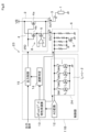
- FIG. 1 is a diagram showing a configuration of a power supply device in a first embodiment
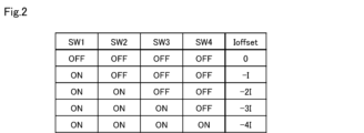
- FIG. 2 is a diagram showing an offset current Ioffset applied in response to the on/off states of the switches SW1 to SW4.
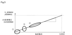
- FIG. 3 is a diagram showing the relationship between the load current and the A/D conversion value when the resistance value of the I/V conversion circuit is only a low resistance
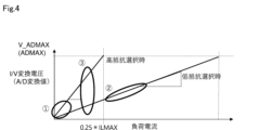
- FIG. 4 is a diagram showing the relationship between a load current and an A/D conversion value when the resistance value of an I/V conversion circuit can be switched between a low resistance and a high resistance
- FIG. 1 is a diagram showing a configuration of a power supply device in a first embodiment
- FIG. 2 is a diagram showing an offset current Ioffset applied in response to the on/off states of the switches SW1 to SW4.
- FIG. 3 is a diagram showing the relationship between the load current and the A/D conversion value when the resistance value of the I/V conversion circuit is only a low resistance
- FIG. 4 is a diagram showing the relationship between
- FIG. 5 is a diagram showing the relationship between the load current and the A/D conversion value when the resistance value of the I/V conversion circuit is switched and the value of the offset current Ioffset is also switched;
- FIG. 6 is a diagram showing a configuration of a power supply device in a second embodiment;
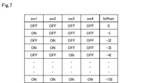
- FIG. 7 is a diagram showing an offset current Ioffset applied in response to the on/off states of the switches sw1 to sw4.
- FIG. 8 is a diagram showing a configuration of a power supply device in a third embodiment;
- FIG. 9 is a diagram showing a relationship between a load current through a constant current circuit and an A/D conversion value;
- FIG. 10 is a diagram showing the relationship between the load current and the A/D conversion value when the resistance value of the I/V conversion circuit is switched and the value of the offset current Ioffset is also switched;
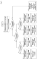
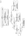
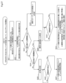
- FIG. 11 is a flowchart showing the processing contents of the control unit in the fourth embodiment.
- FIG. 12 is a diagram showing the relationship between the load current and the A/D conversion value when the resistance value of the I/V conversion circuit is switched and the value of the offset current Ioffset is also switched;
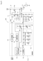
- FIG. 13 is a diagram showing a configuration of a power supply device in a fifth embodiment;
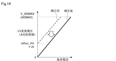
- FIG. 14 is a diagram showing the relationship between the load current and the A/D conversion value when a positive offset current is superimposed on the sense MOS;
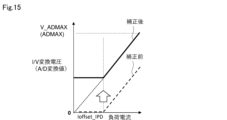
- FIG. 15 is a diagram showing the relationship between the load current and the A/D conversion value when a negative offset current is superimposed on the sense MOS;
- FIG. 16 is a diagram showing the relationship between the load current and the A/D conversion value when the resistance value of the I/V conversion circuit is switched and the value of the offset current Ioffset is also switched;
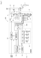
- FIG. 17 is a diagram (part 1) showing a configuration of a power supply device in a sixth embodiment;
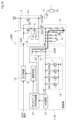
- FIG. 18 is a diagram (part 2) showing the configuration of the power supply device;
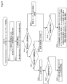
- FIG. 19 is a flowchart showing the processing contents of the control unit;
- FIG. 20 is a diagram (part 1) showing a configuration of a power supply device in the seventh embodiment;
- FIG. 21 is a flowchart showing the processing contents of the control unit;
- FIG. 22 is a diagram showing an example of a table used to determine the type of IPD
- FIG. 23 is a diagram (part 2) showing the configuration of a power supply device
- FIG. 24 is a flowchart showing the processing contents of the control unit in the eighth embodiment.
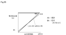
- FIG. 25 is a diagram for explaining a process of applying a linear function to an A/D conversion result for correction
- FIG. 26 is a diagram showing a configuration of a power supply device in a ninth embodiment
- FIG. 27 is a flowchart showing the processing contents of the control unit.
- the power supply device of this embodiment supplies electricity to a load 1, one end of which is connected to ground, from a power source VB via an IPD 2 and a harness 3.
- the IPD 2 has N-channel MOSFETs 4a and 4b, the drain of which is connected to the power source VB and the gates of which are connected in common.
- the source of the FET 4a which is an example of a power device, is connected to the load 1 via the harness 3, and the source of the FET 4b is connected to ground via a P-channel MOSFET 5 and an I/V conversion circuit 6.
- the source of the FET 4b is connected to the inverting input terminal of an operational amplifier 7 together with the source of the FET 5, and the non-inverting input terminal of the operational amplifier 7 is connected to the source of the FET 4a.
- the FETs 4a and 4b form a transistor pair 4.
- the FET 4b is a so-called sense MOS, and the FETs 4b and 5, as well as the operational amplifier 7, form a current output circuit 8.
- the I/V conversion circuit 6 is composed of a combination of seven resistor elements, each of which is a resistor for detecting resistance value R, and a P-channel MOSFET 9.
- a series circuit of two resistor elements R is connected between the source of FET 4b and ground.
- a series circuit of two resistor elements R and a MOSFET 9 is connected in parallel to this series circuit.
- three resistor elements R are connected in parallel to the two resistor elements R.
- the gates of the transistor pair 4 and FET 9 are driven by the control unit 11.
- the resistance value of the I/V conversion circuit 6 is 2R when FET 9 is off, and R/4 when FET 9 is on. In the following, the former may be referred to as "high resistance” and the latter as "low resistance”.
- an A/D converter 12 Inside the control unit 11, an A/D converter 12, an eFuse ( I2 , t) characteristic calculation unit 13, an interruption determination unit 14, and an output control unit 15 are connected in series.
- Data converted by the A/D converter 12 is input to the eFuse ( I2 , t) characteristic calculation unit 13.
- the result of the calculation by the calculation unit 13 is input to the interruption determination unit 14, and the determination result of the interruption determination unit 14 is input to the output control unit 15.
- the eFuse ( I2 , t) characteristic calculation unit 13 performs calculations based on data proportional to the square of the detected current for the data converted by the A/D converter 12, as in the "multiplication circuit 200" shown in Fig. 1 of JP 2023-18957 A, and outputs the result. This is based on the fact that the smoke generation time t of the harness 3 has a characteristic that depends on the square of the current passed through it, as described in the same publication.
- the shutoff determination unit 14 compares the data calculated as described above with a threshold value to determine whether or not to issue a shutoff command.
- the output control unit 15 drives the gates of the transistor pair 4 of the IPD 2 in response to an output command input from a higher-level control device (not shown).
- a shutoff command is input from the shutoff determination unit 14, the output control unit 15, which corresponds to a protection operation unit, turns off the transistor pair 4.
- a sink-side current source section 16 is connected between the input terminal of the A/D converter 12 and ground.
- the sink-side current source section 16 includes a series circuit in which a sink-side current source I is connected to each of the switches SW1 to SW4.
- the on/off control of the FET 9 and the switches SW1 to SW4 is performed by an eFuse ( I2 , t) characteristic calculation section 13.
- the above parts excluding the harness 3 and the load 1 constitute a power supply device 17.
- the offset current flowing to ground due to the operation of the current source I is defined as Ioffset.
- the current Ioffset reduces the current flowing to ground from the IPD2 via the I/V conversion circuit 6.
- the current Ioffset varies in the range of -I to -4I by selectively turning on the switches SW1 to SW4.
- region (1) where the load current value is small, it is difficult to determine whether the load is good or bad and whether it is in a wake-up or sleep state due to the effects of errors caused by A/D conversion.
- region (2) the current measurement resolution is low, so it becomes necessary to perform protective operation by shutting off the IPD 2 earlier than the ideal fusing characteristic of the harness 3.
- Region (3) indicates the current value that can be steadily flowed through the harness 3. Note that the numbers in parentheses correspond to the circled numbers in the figure.
- the load current-I/V conversion characteristic becomes as shown in Fig. 5.
- the load current is IL
- the monitor current flowing to the I/V conversion circuit 6 side is IS
- the current ratio of the I/V conversion circuit 6 is KILIS
- the I/V conversion circuit 6 converts a current based on that current into a voltage by passing it through a detection resistor.
- the A/D converter 12 converts the voltage converted by the I/V conversion circuit 6 into a data value.
- the output control unit 15 performs a protective operation to stop the current supply to the load 1 by the FET 4a.
- the sink side current source unit 16 is configured to be able to superimpose an offset current Ioffset on the current passed through the detection resistor in multiple stages.
- the voltage input to the A/D converter 12 can be further reduced by varying the current Ioffset applied to the current passed through the detection resistor by the multiple current sources I. This makes it possible to virtually improve the resolution of the data conversion in the A/D converter 12.
- the power supply device 21 of the second embodiment includes a sink side current source section 22 replacing the sink side current source section 16.
- the sink side current sources I, 2I, 4I, and 8I are connected to the switches sw1 to sw4, respectively.
- the power supply device 23 of the third embodiment includes a sink-side current source section 24 in place of the sink-side current source section 16.
- ⁇ is Vsat, which is the voltage obtained by adding the minimum resistance value of the I/V conversion circuit 6 to the on-resistance of the FET 4b and multiplying the result by the current flowing therethrough, and when the potential of the ground to which the I/V conversion circuit 6 is connected is displaced higher than 0V, the displacement voltage is Vdiff, and so ⁇ >(Vsat+Vdiff)/(2R)
- a constant current circuit such as the current output circuit 8 cannot operate at a constant current in a region where the input voltage is low, as shown in Figure 9, due to the on-resistance and saturation voltage of the transistors as described above, and the voltage generated in the resistor on the ground side. Therefore, by setting each current source I ⁇ of the sink side current source section 24 to (I- ⁇ ) and overlapping the range below the voltage Vsat as shown in Figure 10, it becomes possible to convert to a voltage in a region where everything is linear by switching the current Ioffset to 0, -I ⁇ , -2I ⁇ , -3I ⁇ , ....
- the fourth embodiment shows the control contents in the control unit 11.
- the A/D conversion result is compared with each of the conversion values adl4 or more to adl1 shown in Fig. 12, and it is determined whether or not it is equal to or more than each of the conversion values adl4 to adl1 (S3 to S6).
- the conversion value adl1 is subtracted by the conversion value adh1 corresponding to the high resistance value of 2R from the A/D conversion result, and the result is added to the maximum conversion value ADMAX to make a digital value continuous with current region A (S12).
- the digital value in step S19 is equal to the result of subtracting the conversion values adh1 to adh3 from four times the maximum conversion value ADMAX, subtracting the conversion value adl1 from the A/D conversion result at low resistance, and then multiplying the result by KR.
- the conversion values adh1 to adh3 are the difference between the A/D conversion values when the sink side current source unit 16 switches the current Ioffset to transition between current regions A to C, and these are stored in advance in memory unit 11M (not shown) provided in control unit 11.
- the A/D conversion values adl1 to adl4 when the I/V conversion circuit 6 is set to a low resistance value are stored in advance, and the actual A/D conversion results are compared with these to separate the cases into current ranges A to E, and for current ranges A to D, the I/V conversion circuit 6 is switched to a high resistance value and A/D conversion is performed again.
- conversion values adh1 to adh3 corresponding to the A/D conversion values adl1 to adl3 when the I/V conversion circuit 6 is set to a low resistance value are also stored in advance, and the final digital value is obtained by subtracting the conversion values adh1 to adh3 from the result of the second A/D conversion.
- a power supply device 25 of the fifth embodiment includes a source side current source 26 and a sink side current source 27 as correction current supply sources in a control unit 11C.
- the source side current source 26 is connected between a power source VB and an input terminal of an A/D converter 12, and the sink side current source 27 is connected between the input terminal and ground. Both of the current sources 26 and 27 are configured to have variable constant current values.
- the variable control is performed by an eFuse ( I2 , t) characteristic calculation unit 13.
- the dynamic range can be expanded by reducing the offset voltage by adjusting the sink current Ioffset_trim to ( ⁇ -Ioffset_IPD) using the sink side current source 27, which has an adjustable constant current value.
- the value of Ioffset_trim in the sink side current source 27 is dynamically controlled to -Ioffset_IPD, -Ioffset_IPD- ⁇ , -Ioffset_IPD- ⁇ , ... so that the variation can be absorbed.
- the sink side current source 27 and the sink side current source unit 16 may be adjusted in cooperation with each other, or the adjustment steps of the sink side current source unit 16 may be finely set to deal with the situation.
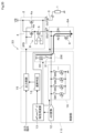
- power supply devices 28I and 28R of the sixth embodiment include source-side current supply sources 29I and 29R as correction current supply sources in control units 11I and 11R, respectively.
- the source-side current supply source 29I is composed of a series circuit of a current source 30 and a switch 31 connected between a power source VB and ground, and the source-side current supply source 29R replaces the current source 30 with a resistor element 32.
- the on/off control of the switch 31 is performed by an eFuse ( I2 , t) characteristic calculation unit 13.
- processing is started in a self-check mode with the output control unit 15 turning off the IPD 2 or putting it in standby.
- the switch 31 of the source side current supply source 29I or 29R is turned on to pass a current through the resistive element of the I/V conversion circuit 6 (S21). It is preferable to initially set the resistance value of the I/V conversion circuit 6 to the low resistance side. Then, A/D conversion is performed by the A/D converter 12, and the resistance value that can be read from the conversion result is determined (S22).
- the determined resistance value is equal to or greater than the upper threshold (S23; Yes)
- a command to execute a diagnosis is sent to a higher-level control device, or the IPD2 is maintained in the off state (S31).
- the determined resistance value is equal to or less than the lower threshold (S24; Yes)
- the same process as in step S31 is performed (S29).
- the determined resistance value exceeds the lower threshold (S24; No)
- the start-up condition is met, for example, by a command from a higher-level control device (S26; Yes)
- the IPD2 is turned on and eFuse control is started (S27).
- the resistance value of the I/V conversion circuit 6 is first set to low resistance and the above determination is made, and if the determination result is normal, the resistance value is switched to high resistance and a similar determination is made. By comparing the first A/D conversion result after switching to high resistance with the A/D conversion result at low resistance, it is possible to determine whether the former A/D conversion result is appropriate. If there is an abnormality, only the connection on the high resistance side can be determined to be abnormal.
- a power supply device 33 of the seventh embodiment is a combination of the control unit 11I of the sixth embodiment and an I/V conversion circuit 6A.
- the I/V conversion circuit 6A includes a resistor R1 as a detection resistor and a resistor R2 connected together with the FET 9, and is configured to switch the resistance value between R1 and a parallel value R1//R2 of R1 and R2.
- the type of IPD 2 connected to the I/V conversion circuit 6A is determined by the resistance values of the resistors R1 and R2.
- the resistance value of the I/V conversion circuit 6A is switched to the high resistance side R1 (S41).
- the switch 31 of the source side current supply source 29I is turned on to pass current through the resistive element of the I/V conversion circuit 6 (S42).
- A/D conversion is performed by the A/D converter 12, and the conversion result is obtained as resistance value data ValR1 (S43).
- the resistance value of the I/V conversion circuit 6A is switched to the low resistance side R1//R2 (S44), A/D conversion is performed by the A/D converter 12, and the conversion result is obtained as resistance value data ValR1_R2 (S45). Then, a control parameter is set from the combination of the resistance value data ValR1 and ValR1_R2 (S46).
- the control unit 11I holds a data table for determining the type of IPD2, for example, as shown in FIG. 22.
- FIG. 21 shows a configuration using a control unit 35 in which a microcomputer 34 is added to the control unit 11I.
- the microcomputer 34 may be provided with a function for monitoring the output control unit 15, and parameters may be set for the operation when the microcomputer 34 detects an abnormality, such as forced on or forced off, or maintaining the previous operation.
- a source side current supply source 29R may be used instead of the source side current supply source 29I.
- the connection state of the I/V conversion circuit 6 is judged as in the sixth embodiment. After steps S28 and S30 are executed, it is judged whether the start-up condition is satisfied (S32) as in step S26. If the start-up condition is satisfied (Yes), for example, when correcting the A/D conversion result using a linear function, the intercept (offset) parameter Bh shown in Fig. 25 is changed to a value larger than the value normally used (S33).
- the correction value of the A/D conversion result makes it possible to recognize that a large current is flowing regardless of the actual load current IL.
- the eFuse control function or power monitoring function operates in a short time to provide protection that cuts off the current, making it possible to safely protect the load 1.
- the ninth embodiment is a variation of the eighth embodiment.
- a normally-closed switch 36 is inserted between the input terminal of the A/D converter 12 and the sink-side current source unit 16, and the source-side current source 29I of the sixth embodiment is connected to the common connection point between the input terminal and the switch 36.
- the on/off control of the switch 36 is performed by the eFuse ( I2 , t) characteristic calculation unit 13. Then, as shown in FIG. 27, if the result of step S32 is "Yes," the switch 36 is turned off, and the switch 31 of the source-side current source 29I is turned on (S34).
- the resistance value in the I/V conversion circuit may be changed in three or more stages. Also, it is not always necessary to change the resistance value.
- the number of current sources provided in the sink side current source section may be "3" or less, or "5" or more.
- the A/D converter 12 and the eFuse (I 2 , t) characteristic calculation unit 13 may be integrated to configure a data converter that outputs a conversion result according to the two-wire characteristic of the current.
- the third embodiment may be applied to the second, fourth to ninth embodiments, and the like. Applicable embodiments may be combined as appropriate.
- this case includes the following inventions: [1] a power device (4a) that supplies current from a driving power supply (VB) to a load (1); an I/V conversion circuit (6, 6A) that converts a current based on the current into a voltage by passing a current through a detection resistor (R, R1, R2) and detects the voltage; a data converter (12) for converting the voltage converted by the I/V conversion circuit into a data value based on a predetermined characteristic; a protection operation unit (13 to 15) that performs a protection operation to stop a current supply to a load by the power device when a calculated value based on the data value exceeds a threshold value; a power supply device including a plurality of sink-side current sources (I, I ⁇ , 2I, 3I, 4I) configured to be able to superimpose an offset value for a current flowing through the detection resistor in multiple stages.
- I/V conversion circuit (6, 6A) that converts a current based on the current into a voltage by passing
- the I/V conversion circuit is configured to be capable of switching current flow to two or more detection resistors having different resistance values;
- a current output circuit (8) is provided for outputting a current proportional to a load current flowing through the power device,
- the power supply device according to any one of [1] to [4], further comprising a correction current supply source for correcting an offset current generated in the current output circuit.
- a source-side current supply source (29I, 29R) for supplying current to the detection resistor in a state where the power device stops supplying current to the load,
- the power supply device according to any one of [1] to [5], wherein the control unit determines whether the detection resistor is abnormal based on a result of data conversion associated with the energization.
- control unit has a correction unit that corrects the output data of the data converter
- the power supply device further comprising: a correction unit that sets a correction parameter for the correction unit so that the protective operation unit starts the protective operation more quickly when an abnormality is detected in the detection resistor.
- control unit sets the input voltage of the data converter to a high potential when it determines that the detection resistor is abnormal.
- a source-side current supply source (29I, 29R) for supplying current to the detection resistor in a state where the power device stops supplying current to the load
- the power supply device according to any one of [1] to [8], wherein the control unit determines the type of the connected power device based on the result of the data conversion associated with the energization, and sets control parameters according to the determined type.
Landscapes
- Engineering & Computer Science (AREA)
- Physics & Mathematics (AREA)
- General Physics & Mathematics (AREA)
- Power Engineering (AREA)
- Mechanical Engineering (AREA)
- Dc-Dc Converters (AREA)
- Electromagnetism (AREA)
- Radar, Positioning & Navigation (AREA)
- Automation & Control Theory (AREA)
- Emergency Protection Circuit Devices (AREA)
Abstract
駆動用電源VBよりFET4aを介して負荷1に電流を供給する際に、I/V変換回路6は、その電流に基づいた電流を、検出用抵抗に通電することで電圧に変換する。A/D変換器12は、I/V変換回路6により変換された電圧をデータ値に変換する。出力制御部15は、そのデータ値を元にした演算値が閾値を超えると、FET4aによる負荷1への電流供給を停止させる保護動作を行なう。シンク側電流源部16を、検出用抵抗に通電される電流に対するオフセット電流Ioffsetを、多段階で重畳可能に構成する。
Description
本出願は、2023年6月29日に出願された日本出願番号2023-107120号に基づくもので、ここにその記載内容を援用する。
本開示は、駆動用電源より負荷に電流を供給するパワーデバイスを備える電力供給装置に関する。
例えば特許文献1,2には、ワイヤハーネスや負荷の保護のため、半導体スイッチを用いてヒューズ機能を実現する手法が提案されている。以下では、このような保護機能をeFuse制御と称する場合がある。eFuse制御を実現するためには、ワイヤハーネスの熱的時定数により大電流時には短時間で遮断が必要な一方で、ハーネスの細線化によるコスト低減を図るには、ハーネスに定常的に流せる限界電流付近における電流検出精度を向上させる必要がある。
電流検出精度を向上させるため、半導体スイッチに流れる電流をモニタするための出力に対して、I/V変換用の抵抗を2種類用意し、電流範囲に応じて切り替える手法がある。この場合、高抵抗から低抵抗に切り替えて測定が必要となる電流領域では、電流の測定分解能が低下し、理想的な溶断特性よりも早い時間で遮断するように保護動作させる必要が生じる。また、高抵抗側について、ハーネスに定常的に流せる電流付近での電流検出精度が確保できる抵抗値を選定する必要があり、負荷電流が小さい領域での測定分解能低下とA/D変換誤差とにより、負荷の良否判定やウェイクアップ/スリープ等の負荷の状態の把握が難しい。その対策として、抵抗値の種類を増やすとコストが嵩んでしまうという問題があった。
本開示は上記事情に鑑みてなされたものであり、その目的は、コストの上昇を抑制しながら、電流検出の分解能を向上させることができる電力供給装置を提供することにある。
本開示の電力供給装置によれば、駆動用電源(VB)よりパワーデバイスを介して負荷に電流を供給する際に、I/V変換回路は、前記電流に基づいた電流を、検出用抵抗に通電することで電圧に変換する。尚、パワーデバイスとは、例えばインバータのような電力変換回路を構成する、比較的大きな電力をスイッチングするのに対応した半導体素子である。データ変換器は、I/V変換回路により変換された電圧を、所定の特性に基づいたデータ値に変換する。保護動作部は、そのデータ値を元にした演算値が閾値を超えると、パワーデバイスによる負荷への電流供給を停止させる保護動作を行なう。複数のシンク側電流源は、検出用抵抗に通電される電流に対するオフセット値を、多段階で重畳可能に構成される。
このように構成すれば、複数のシンク側電流源により、検出用抵抗に通電される電流に付与するオフセット値を変化させれば、データ変換器に入力される電圧をより低下させることができる。これにより、データ変換器におけるデータ変換の分解能を疑似的に向上させることが可能になる。
また、本開示の電力供給装置によれば、複数のシンク側電流源を、オフセット値を切り替える境界において、切替え前後でI/V変換回路により変換された電圧が、データ変換器の入力範囲内に収まるように設定する。これにより、オフセット値を付与することで、I/V変換回路により変換された電圧が小さい領域で、シンク側電流源の出力特性が非線形となる場合にはオフセット値を少ない側に切替え、シンク側電流源の出力特性が線形となるようにすれば、出力特性を全体に亘って線形にすることができる。
また、本開示の電力供給装置によれば、記憶部に、複数のシンク側電流源を切り替える際の前記データ値の差を予め記憶する。制御部は、複数のシンク側電流源を切り替える際に、対応する差の値を記憶部より読み出して減算する。これにより、使用するシンク側電流源を切り替える際の演算処理が簡単になる。
また、本開示の電力供給装置によれば、I/V変換回路を、抵抗値が異なる2個以上の検出用抵抗への通電が切り替え可能に構成する。先ず、オフセット値を付与せずに、最も低抵抗値の検出用抵抗に通電した状態で第1データ変換を行うと、次に、第1データ変換の結果に応じて選択された、前記の検出抵抗よりも高抵抗値の検出用抵抗に通電した状態で第2データ変換を行う際に、前1データ変換の結果に応じて重畳するオフセット値を決定する。これにより、多くとも2回のデータ変換によって、電流検出を高精度で行うことができる。
本開示についての上記目的およびその他の目的、特徴や利点は、添付の図面を参照しながら下記の詳細な記述により、より明確になる。その図面は、
図1は、第1実施形態において、電力供給装置の構成を示す図であり、
図2は、スイッチSW1~SW4のオンオフ状態に応じて付与されるオフセット電流Ioffsetを示す図であり、
図3は、I/V変換回路の抵抗値が低抵抗だけの場合の負荷電流とA/D変換値との関係を示す図であり、
図4は、I/V変換回路の抵抗値が、低抵抗と高抵抗との切替え可能な場合の負荷電流とA/D変換値との関係を示す図であり、
図5は、I/V変換回路の抵抗値を切替えると共に、オフセット電流Ioffsetの値を切り替えた場合の負荷電流とA/D変換値との関係を示す図であり、
図6は、第2実施形態において、電力供給装置の構成を示す図であり、
図7は、スイッチsw1~sw4のオンオフ状態に応じて付与されるオフセット電流Ioffsetを示す図であり、
図8は、第3実施形態において、電力供給装置の構成を示す図であり、
図9は、定電流回路を介した負荷電流とA/D変換値との関係を示す図であり、
図10は、I/V変換回路の抵抗値を切替えると共に、オフセット電流Ioffsetの値を切り替えた場合の負荷電流とA/D変換値との関係を示す図であり、
図11は、第4実施形態において、制御部の処理内容を示すフローチャートであり、
図12は、I/V変換回路の抵抗値を切替えると共に、オフセット電流Ioffsetの値を切り替えた場合の負荷電流とA/D変換値との関係を示す図であり、
図13は、第5実施形態において、電力供給装置の構成を示す図であり、
図14は、センスMOSに正のオフセット電流が重畳されている場合の負荷電流とA/D変換値との関係を示す図であり、
図15は、センスMOSに負のオフセット電流が重畳されている場合の負荷電流とA/D変換値との関係を示す図であり、
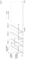
図16は、I/V変換回路の抵抗値を切替えると共に、オフセット電流Ioffsetの値を切り替えた場合の負荷電流とA/D変換値との関係を示す図であり、
図17は、第6実施形態において、電力供給装置の構成を示す図(その1)であり、
図18は、同電力供給装置の構成を示す図(その2)であり、
図19は、制御部の処理内容を示すフローチャートであり、
図20は、第7実施形態において、電力供給装置の構成を示す図(その1)であり、
図21は、制御部の処理内容を示すフローチャートであり、
図22は、IPDの種類を判別するために使用するテーブルの一例を示す図であり、
図23は、電力供給装置の構成を示す図(その2)であり、
図24は、第8実施形態において、制御部の処理内容を示すフローチャートであり、
図25は、A/D変換結果に1次関数を適用して補正する処理を説明する図であり、
図26は、第9実施形態において、電力供給装置の構成を示す図であり、
図27は、制御部の処理内容を示すフローチャートである。
(第1実施形態)
図1に示すように、本実施形態の電力供給装置は、一端がグランドに接続されている負荷1に対し、電源VBよりIPD2及びハーネス3を介して通電を行なう。IPD2は、ドレインが電源VBに接続され、ゲートが共通に接続されたNチャネルMOSFET4a,4bを備えている。パワーデバイスの一例であるFET4aのソースは、ハーネス3を介して負荷1に接続され、FET4bのソースは、PチャネルMOSFET5及びI/V変換回路6を介してグランドに接続されている。また、FET4bのソースは、FET5のソースと共にオペアンプ7の反転入力端子に接続されており、同非反転入力端子はFET4aのソースに接続されている。FET4a及び4bは、トランジスタ対4を構成する。FET4bは所謂センスMOSであり、FET4b及び5、並びにオペアンプ7は、電流出力回路8を構成する。
図1に示すように、本実施形態の電力供給装置は、一端がグランドに接続されている負荷1に対し、電源VBよりIPD2及びハーネス3を介して通電を行なう。IPD2は、ドレインが電源VBに接続され、ゲートが共通に接続されたNチャネルMOSFET4a,4bを備えている。パワーデバイスの一例であるFET4aのソースは、ハーネス3を介して負荷1に接続され、FET4bのソースは、PチャネルMOSFET5及びI/V変換回路6を介してグランドに接続されている。また、FET4bのソースは、FET5のソースと共にオペアンプ7の反転入力端子に接続されており、同非反転入力端子はFET4aのソースに接続されている。FET4a及び4bは、トランジスタ対4を構成する。FET4bは所謂センスMOSであり、FET4b及び5、並びにオペアンプ7は、電流出力回路8を構成する。
I/V変換回路6は、それぞれ抵抗値Rの検出用抵抗である7つの抵抗素子と、PチャネルMOSFET9との組み合わせで構成されている。FET4bのソースとグランドとの間には、2つの抵抗素子Rの直列回路が接続されている。この直列回路には、2つの抵抗素子R及びMOSFET9の直列回路が並列に接続されている。また、上記の2つの抵抗素子Rには、3本の抵抗素子Rが並列に接続されている。トランジスタ対4及びFET9のゲートは、制御部11により駆動される。I/V変換回路6の抵抗値は、FET9がオフであれば2Rであり、FET9がオンすればR/4になる。以下では、前者を「高抵抗」、後者を「低抵抗」と称する場合がある。t)
制御部11の内部では、A/D変換器12、eFuse(I2,t)特性用演算部13、遮断判定部14、及び出力制御部15がシリアルに接続されている。データ変換器の一例であるA/D変換器12の入力端子は、IPD2及びI/V変換回路6の共通接続点に接続されている。A/D変換器12により変換されたデータは、eFuse(I2,t)特性用演算部13に入力される。演算部13が演算した結果は遮断判定部14に入力され、遮断判定部14の判定結果は、出力制御部15に入力される。
eFuse(I2,t)特性用演算部13は、例えば特開2023-18957号公報の図1に示す「乗算回路200」のように、A/D変換器12により変換されたデータについて、検出した電流の2乗に比例したデータを元に演算して出力する。これは、同公報中に記載されているように、ハーネス3の発煙時間tが、通電される電流の2乗に依存した特性を備えることに基づいている。
遮断判定部14は、上記のように演算されたデータを閾値と比較することで、遮断指示を行うか否かを判定する。出力制御部15は、図示しない上位の制御装置から入力される出力指示に応じて、IPD2のトランジスタ対4のゲートを駆動する。また、遮断判定部14より遮断指示が入力されると、保護動作部に相当する出力制御部15は、トランジスタ対4をオフにする。
A/D変換器12の入力端子とグランドとの間には、シンク側電流源部16が接続されている。シンク側電流源部16は、スイッチSW1~SW4のそれぞれに、シンク側の電流源Iを接続した直列回路を備えている。FET9及びスイッチSW1~SW4のオンオフ制御は、eFuse(I2,t)特性用演算部13によって行われる。以上において、ハーネス3及び負荷1を除いた部分が電力供給装置17を構成する。
次に、本実施形態の作用について説明する。シンク側電流源部16において、電流源Iの動作によりグランドに流れるオフセット電流をIoffsetとする。電流Ioffsetは、IPD2よりI/V変換回路6を介してグランドに流れる電流を減少させる。図2に示すように、スイッチSW1~SW4を択一的にオンにすることで、電流Ioffsetは、-I~-4Iの範囲で変化する。
図3に示すように、電流Ioffsetを流さず、I/V変換回路6を低抵抗状態にした場合の負荷電流-I/V変換特性において、負荷電流値が小さい領域(1)では、A/D変換による誤差の影響もあるため、負荷の良否判定や、ウェイクアップ/スリープ状態の判定が困難になる。また、領域(2)では、電流の測定分解能が低いため、IPD2をハーネス3の理想的な溶断特性よりも早い時間で遮断するように保護動作をさせる必要が生じる。領域(3)は、ハーネス3に定常的に流せる電流値を示す。尚、括弧付きの数字は、図中の丸数字に対応している。
図3に、I/V変換回路6を高抵抗状態にした場合の特性を加えると、図4に示すようになる。このように、高抵抗に切り換えた場合でも、領域(3)の付近での電流検出精度が確保できるように抵抗値を選定する必要がある。
そして、本実施形態のように電流Ioffsetを変化させると、負荷電流-I/V変換特性は、図5に示すようになる。ここで、負荷電流をIL、I/V変換回路6側に流れるモニタ用の電流をIS、I/V変換回路6の電流比をKILISとすると、電流IL、ISの関係は(IL=KILIS×IS)となる。I/V変換回路6に生じる電圧をVsとすると、I/V変換回路6を高抵抗側に選択した場合は、
Vs=(IL/KILIS+Ioffset)×2R
I/V変換回路6を低抵抗側に選択すると
Vs=(IL/KILIS+ offset)×R/4
となる。検出の上限電流をILMAXとすると、
Vs=(ILMAX/KILIS)×R/4=V_ADMAX
となる。
Vs=(IL/KILIS+Ioffset)×2R
I/V変換回路6を低抵抗側に選択すると
Vs=(IL/KILIS+ offset)×R/4
となる。検出の上限電流をILMAXとすると、
Vs=(ILMAX/KILIS)×R/4=V_ADMAX
となる。
オフセット電流Ioffsetを付加しない場合、負荷電流ILは
IL=0~0.125/ILMAXの範囲までしか検出できない。これに対して、本実施形態では、電流源の電流Iを(=V_ADMAX/2R)に設定し、I/V変換回路6を高抵抗側に選択した状態で、オフセット電流Ioffsetを0から-I、-2I、-3Iと段階的に増やして行く。
IL=0~0.125/ILMAXの範囲までしか検出できない。これに対して、本実施形態では、電流源の電流Iを(=V_ADMAX/2R)に設定し、I/V変換回路6を高抵抗側に選択した状態で、オフセット電流Ioffsetを0から-I、-2I、-3Iと段階的に増やして行く。
電流Ioffset=-Iにすると、負荷電流ILは
IL=0.125×ILMAX~0.25×ILMAX
の範囲で検出ができるようになる。更に、電流Ioffset=-2I、-3Iにすれば、
IL=0.25×ILMAX~0.5×ILMAX
の範囲が検出可能になり、電流Ioffset=-4Iにすれば、0.75×ILMAX範囲が検出可能になる。すなわち、従来はIL=0~0.25×ILMAXの範囲で、低抵抗切替時の4倍の分解能であったものを、本実施形態の手法では、領域(1)~(3)の全てで電流検出分解能を8倍に高めることができ、A/D変換器12の誤差の影響を低減することができる。
IL=0.125×ILMAX~0.25×ILMAX
の範囲で検出ができるようになる。更に、電流Ioffset=-2I、-3Iにすれば、
IL=0.25×ILMAX~0.5×ILMAX
の範囲が検出可能になり、電流Ioffset=-4Iにすれば、0.75×ILMAX範囲が検出可能になる。すなわち、従来はIL=0~0.25×ILMAXの範囲で、低抵抗切替時の4倍の分解能であったものを、本実施形態の手法では、領域(1)~(3)の全てで電流検出分解能を8倍に高めることができ、A/D変換器12の誤差の影響を低減することができる。
以上のように本実施形態によれば、駆動用電源VBよりFET4a及びハーネス3を介して負荷1に電流を供給する際に、I/V変換回路6は、その電流に基づいた電流を、検出用抵抗に通電することで電圧に変換する。A/D変換器12は、I/V変換回路6により変換された電圧をデータ値に変換する。出力制御部15は、そのデータ値を元にした演算値が閾値を超えると、FET4aによる負荷1への電流供給を停止させる保護動作を行なう。そして、シンク側電流源部16を、検出用抵抗に通電される電流に対するオフセット電流Ioffsetを、多段階で重畳可能に構成する。
このように構成すれば、複数の電流源Iにより、検出用抵抗に通電される電流に付与する電流Ioffsetを変化させれば、A/D変換器12に入力される電圧をより低下させることができる。これにより、A/D変換器12におけるデータ変換の分解能を疑似的に向上させることが可能になる。
(第2実施形態)
以下、第1実施形態と同一部分には同一符号を付して説明を省略し、異なる部分について説明する。図6に示すように、第2実施形態の電力供給装置21は、シンク側電流源部16に替わるシンク側電流源部22を備えている。シンク側電流源部22は、スイッチsw1~sw4のそれぞれに、シンク側の電流源I、2I,4I及び8Iが接続されている。このように構成すれば、図7に示すように、スイッチsw1~sw4のオンオフを4ビットのデータに対応させて「1~15」となるように変化させれば、それに応じて電流Ioffsetを「-I~-15I」の範囲で変化させることができる。
以下、第1実施形態と同一部分には同一符号を付して説明を省略し、異なる部分について説明する。図6に示すように、第2実施形態の電力供給装置21は、シンク側電流源部16に替わるシンク側電流源部22を備えている。シンク側電流源部22は、スイッチsw1~sw4のそれぞれに、シンク側の電流源I、2I,4I及び8Iが接続されている。このように構成すれば、図7に示すように、スイッチsw1~sw4のオンオフを4ビットのデータに対応させて「1~15」となるように変化させれば、それに応じて電流Ioffsetを「-I~-15I」の範囲で変化させることができる。
(第3実施形態)
図8に示すように、第3実施形態の電力供給装置23は、シンク側電流源部16に替わるシンク側電流源部24を備えている。シンク側電流源部24は、定電流値がそれぞれIδ=(I-δ)となる4つの電流源Iδで構成されている。ここでδは、FET4bのオン抵抗にI/V変換回路6の最小抵抗値を加えて、それらに流れる電流を乗じた電圧をVsat,I/V変換回路6が接続されているグランドの電位が0Vよりも高い方に変位している場合に、その変位電圧をVdiffとすると
δ>(Vsat+Vdiff)/(2R)
に設定する。定電流値Iは、第1実施形態と同様の(=V_ADMAX/2R)である。
図8に示すように、第3実施形態の電力供給装置23は、シンク側電流源部16に替わるシンク側電流源部24を備えている。シンク側電流源部24は、定電流値がそれぞれIδ=(I-δ)となる4つの電流源Iδで構成されている。ここでδは、FET4bのオン抵抗にI/V変換回路6の最小抵抗値を加えて、それらに流れる電流を乗じた電圧をVsat,I/V変換回路6が接続されているグランドの電位が0Vよりも高い方に変位している場合に、その変位電圧をVdiffとすると
δ>(Vsat+Vdiff)/(2R)
に設定する。定電流値Iは、第1実施形態と同様の(=V_ADMAX/2R)である。
一般に、電流出力回路8のような定電流回路は、上記のようなトランジスタのオン抵抗や飽和電圧、グランド側の抵抗に発生する電圧によって、図9に示すように、入力される電圧が低い領域では定電流動作ができない。そこで、シンク側電流源部24の各電流源Iδを(I-δ)に設定し、図10に示すように、電圧Vsat以下の範囲をオーバーラップさせれば、電流Ioffsetを0、-Iδ,-2Iδ,-3Iδ,…に切り換えることで、全てが線形となる領域で電圧に変換できるようになる。
(第4実施形態)
図11に示すように、第4実施形態は、制御部11における制御内容を示す。処理をスタートすると、I/V変換回路6の抵抗値を低い側の(R/4)に設定し(S1)、電流Ioffset=0でA/D変換を行う(S2)。これが第1データ変換に相当する。そして、そのA/D変換結果を、図12に示す各変換値adl4以上~adl1と比較し、各変換値adl4~adl1以上か否かを判断する(S3~S6)。
図11に示すように、第4実施形態は、制御部11における制御内容を示す。処理をスタートすると、I/V変換回路6の抵抗値を低い側の(R/4)に設定し(S1)、電流Ioffset=0でA/D変換を行う(S2)。これが第1データ変換に相当する。そして、そのA/D変換結果を、図12に示す各変換値adl4以上~adl1と比較し、各変換値adl4~adl1以上か否かを判断する(S3~S6)。
A/D変換結果が変換値adl4以上であれば(S3;Yes)、図12に示す電流領域E(IL4~ILMAX)に属することになる。I/V変換回路6の低抵抗値と高抵抗値との比をKRとすると、A/D変換結果をKR倍したものを、検出した電流に応じた最終的なデジタル値とする(S19)。第4実施形態の場合、KR=8である。尚、図中に示す「理想特性の場合」とは、説明を簡単にするため、第3実施形態のように、低電流領域において変換特性が非線形となる場合を無視していることによる。
A/D変換結果が変換値adl1未満であれば(S5;No)電流領域A(0~IL1)に属しており、I/V変換回路6の抵抗値を高い側の2Rに切り替えて(S7)、ステップS2と同様にA/D変換を行う(S8)。そして、A/D変換結果をそのまま最終的なデジタル値とする(S9)。A/D変換結果が変換値adl2未満で且つ変換値adl1以上であれば(S5;Yes)電流領域B(IL1~IL2)に属しており、ステップS7と同様の処理を行い(S10)、電流Ioffset=-IでA/D変換を行う(S11)。そして、そのA/D変換結果より、変換値adl1に高抵抗値2Rの場合に対応する変換値adh1を減じたものを最高変換値ADMAXに加えることで、電流領域Aに連続するデジタル値にする(S12)。
A/D変換結果が変換値adl2以上で且つ変換値adl3未満であれば(S6;No)電流領域C(IL2~IL3)に属しており、ステップS7と同様の処理を行い(S13)、電流Ioffset=-2IでA/D変換を行う(S14)。そして、そのA/D変換結果より、変換値adh1、及び変換値adl2に高抵抗値2Rの場合に対応する値変換値adh2を減じたものを最高変換値ADMAXの2倍値に加えることで、電流領域Bに連続するデジタル値にする(S15)。
A/D変換結果が変換値adl4未満で且つ変換値adl3以上であれば(S6;Yes)電流領域D(IL3~IL4)に属しており、ステップS7と同様の処理を行い(S16)、電流Ioffset=-3IでA/D変換を行う(S17)。そして、そのA/D変換結果より、変換値adh1及びadh2、並びに変換値adl3に高抵抗値2Rの場合に対応する値変換値adh3を減じたものを最高変換値ADMAXの3倍値に加えることで、電流領域Cに連続するデジタル値にする(S15)。ステップS8,S11,S14S及びS17は、第2データ変換に相当する。
尚、ステップS19におけるデジタル値、低抵抗でのA/D変換結果をKR倍したものは、最高変換値ADMAXの4倍値より変換値adh1~adh3を減じて、更に低抵抗でのA/D変換結果より変換値adl1を減じた値をKR倍したものを加えた結果に等しくなる。また、変換値adh1~adh3は、シンク側電流源部16により電流Ioffsetを切り替えて、電流領域A~Cの領域間を移行する際におけるA/D変換値の差であり、これらは予め、制御部11が備える図示しない記憶部11Mに記憶されている。
以上のように第4実施形態によれば、I/V変換回路6を低抵抗値に設定した場合のA/D変換値adl1~adl4を予め記憶しておき、実際のA/D変換結果をそれらと比較することで電流領域A~Eに場合分けし、電流領域A~DについてはI/V変換回路6を高抵抗値に切り替えて再度A/D変換する。また、I/V変換回路6を低抵抗値に設定した場合の、A/D変換値adl1~adl3に対応した変換値adh1~adh3も予め記憶しておき、再度のA/D変換結果より、変換値adh1~adh3を減算する等して最終的なデジタル値を得る。これにより、最大2回のA/D変換により、電流領域A~Dにおける変換分解能を疑似的に高めることができる。ここで、ステップS11、ステップS17では例外処理を省略して記載しているが、入力電圧がA/D変換器12の入力電圧の上限を上回った場合は、ステップS19の方法でデジタル値を得るようにしても良い。
(第5実施形態)
図13に示すように、第5実施形態の電力供給装置25は、制御部11Cに補正用電流供給源として、ソース側電流源26及びシンク側電流源27を備えている。ソース側電流源26は、電源VBとA/D変換器12の入力端子との間に接続され、シンク側電流源27は、上記の入力端子とグランドとの間に接続されている。電流源26及び27は、何れも定電流値が可変に構成されている。その可変制御は、eFuse(I2,t)特性用演算部13によって行われる。
図13に示すように、第5実施形態の電力供給装置25は、制御部11Cに補正用電流供給源として、ソース側電流源26及びシンク側電流源27を備えている。ソース側電流源26は、電源VBとA/D変換器12の入力端子との間に接続され、シンク側電流源27は、上記の入力端子とグランドとの間に接続されている。電流源26及び27は、何れも定電流値が可変に構成されている。その可変制御は、eFuse(I2,t)特性用演算部13によって行われる。
IPD2において、センスMOSであるFET4bに、正のオフセット電流Ioffset_IPDが重畳されていると、負荷電流ILとモニタ用電流出力ISの関係は、
IL=KILIS×IS+Ioffset_IPD
となる。そのため、図14に破線で示すようにI/V変換回路6の抵抗値が高い2Rの場合には、負荷電流IL=0Aの状態で、オフセット電圧(Ioffset_IPD×2R)が発生し、ダイナミックレンジが圧迫されてしまう。
IL=KILIS×IS+Ioffset_IPD
となる。そのため、図14に破線で示すようにI/V変換回路6の抵抗値が高い2Rの場合には、負荷電流IL=0Aの状態で、オフセット電圧(Ioffset_IPD×2R)が発生し、ダイナミックレンジが圧迫されてしまう。
これに対して、定電流値を調整可能なシンク側電流源27によりシンク電流Ioffset_trimを(≒-Ioffset_IPD)になるように調整して流すことでオフセット電圧を低減すれば、ダイナミックレンジを拡大することができる。
また、FET4bに、負のオフセット電流Ioffset_IPDが重畳されていれば、負荷電流ILとモニタ用電流出力ISの関係は、
IL=KILIS×IS-Ioffset_IPD
となる。そのため、図15に破線で示すように、負荷電流ILが0A~Ioffset_IPDの範囲ではA/D変換値がほぼゼロになり、負荷電流ILがそれより大きい領域でも、A/D変換値が本来の値よりも低い値となる。これはでは、ハーネス3に過電流による焼損が発生することを防止するための保護が、効き難くなる方向にズレてしまう。そこで、定電流値を調整可能なソース側電流源26によりソース電流Ioffset_trimを(≒-Ioffset_IPD)になるように調整して流すことで、ハーネス3の保護機能を低下させることなく維持できる。
IL=KILIS×IS-Ioffset_IPD
となる。そのため、図15に破線で示すように、負荷電流ILが0A~Ioffset_IPDの範囲ではA/D変換値がほぼゼロになり、負荷電流ILがそれより大きい領域でも、A/D変換値が本来の値よりも低い値となる。これはでは、ハーネス3に過電流による焼損が発生することを防止するための保護が、効き難くなる方向にズレてしまう。そこで、定電流値を調整可能なソース側電流源26によりソース電流Ioffset_trimを(≒-Ioffset_IPD)になるように調整して流すことで、ハーネス3の保護機能を低下させることなく維持できる。
また、シンク側電流源部16の電流値を、-I,-2I,…に制御する際に、各電流源I値にそれぞれ、-I+α,-2I+β,…といったばらつきが生じる場合には、そのばらつきを吸収できるように、シンク側電流源27におけるIoffset_trimの値を-Ioffset_IPD、-Ioffset_IPD-α、-Ioffset_IPD-β,…と動的に制御する。これにより、図16中に(4)で示すように、正しくデジタル値に変換できない領域が発生することを防ぎ、負荷電流ILを高分解能で検出できる電流範囲を拡大できる。尚、シンク側電流源27と、シンク側電流源部16とを協働させて調整しても良く、シンク側電流源部16の調整ステップを細かく設定して対応する等しても良い。
(第6実施形態)
図17及び図18に示すように、第6実施形態の電力供給装置28I,28Rは、制御部11I,11Rに補正用電流供給源として、それぞれソース側電流供給源29I,29Rを備えている。ソース側電流供給源29Iは、電源VBとグランドとの間に接続される電流源30及びスイッチ31の直列回路で構成され、ソース側電流供給源29Rは、上記の電流源30を抵抗素子32に置換えたものである。スイッチ31のオンオフ制御は、eFuse(I2,t)特性用演算部13によって行われる。
図17及び図18に示すように、第6実施形態の電力供給装置28I,28Rは、制御部11I,11Rに補正用電流供給源として、それぞれソース側電流供給源29I,29Rを備えている。ソース側電流供給源29Iは、電源VBとグランドとの間に接続される電流源30及びスイッチ31の直列回路で構成され、ソース側電流供給源29Rは、上記の電流源30を抵抗素子32に置換えたものである。スイッチ31のオンオフ制御は、eFuse(I2,t)特性用演算部13によって行われる。
次に、第6実施形態の作用について説明する。図19に示すように、出力制御部15がIPD2をオフさせているか又はスタンバイにしている状態で、セルフチェックを行うモードで処理を開始する。先ず、ソース側電流供給源29I又は29Rのスイッチ31をオンにして、I/V変換回路6の抵抗素子に電流を流す(S21)。尚、I/V変換回路6の抵抗値の設定は、最初に低抵抗値側しておくのが望ましい。そして、A/D変換器12によりA/D変換を行い、その変換結果より読み取れる抵抗値を判定する(S22)。
判定した抵抗値が上限閾値以上であれば(S23;Yes)、I/V変換回路6の接続がオープンとなっているか天絡している疑いがあるので、異常と判定する(S30)。そして、例えば上位の制御装置等にダイアグ実行の指令を送信するか、IPD2のオフ状態をそのまま維持する(S31)。
判定した抵抗値が下限閾値以下であれば(S24;Yes)、I/V変換回路6の接続が地絡している疑いがあるので、異常と判定する(S28)。そして、ステップS31と同様の処理を行う(S29)。一方、判定した抵抗値が下限閾値を超えていれば(S24;No)正常と判定する(S25)。そして、例えば上位の制御装置からの指令等により起動条件が成立すれば(S26;Yes)、IPD2をオンにしてeFuse制御を開始する(S27)。
このように、IPD2をオフ等にした状態で、ソース側電流供給源29を介してI/V変換回路6にソース電流を流した際の抵抗値を判定することで、I/V変換回路6の接続が正常か、異常かを判定できる。また、I/V変換回路6の抵抗値の設定を最初に低抵抗にして上記の判定を行ない、判定結果が正常であれば、抵抗値の設定を高抵抗に切り替えて同様の判定を行なう。高抵抗に切り替えた後の最初のA/D変換結果を、低抵抗時のA/D変換結果と比較することで、前者のA/D変換結果が適正か否かを判定できる。異常であれば、高抵抗側の接続のみが異常と判定できる。
(第7実施形態)
図20に示すように、第7実施形態の電力供給装置33は、第6実施形態の制御部11IとI/V変換回路6Aとの組み合わせである。I/V変換回路6Aは、検出用抵抗として抵抗R1とFET9と共に接続される抵抗R2とを備えており、抵抗値をR1と、R1及びR2の並列値R1//R2とに切替える構成である。第7実施形態では、抵抗R1、R2の抵抗値によって、I/V変換回路6Aに接続されるIPD2の種類を判別する。
図20に示すように、第7実施形態の電力供給装置33は、第6実施形態の制御部11IとI/V変換回路6Aとの組み合わせである。I/V変換回路6Aは、検出用抵抗として抵抗R1とFET9と共に接続される抵抗R2とを備えており、抵抗値をR1と、R1及びR2の並列値R1//R2とに切替える構成である。第7実施形態では、抵抗R1、R2の抵抗値によって、I/V変換回路6Aに接続されるIPD2の種類を判別する。
次に、第7実施形態の作用について説明する。図21に示すように、第6実施形態と同じ状態で、セルフチェックを行うモードで処理を開始すると、I/V変換回路6Aの抵抗値を高抵抗側のR1に切り替える(S41)。ソース側電流供給源29Iのスイッチ31をオンにして、I/V変換回路6の抵抗素子に電流を流す(S42)。そして、A/D変換器12によりA/D変換を行い、その変換結果を抵抗値データValR1として取得する(S43)。
続いて、I/V変換回路6Aの抵抗値を低抵抗側のR1//R2に切り替えて(S44)、A/D変換器12によりA/D変換を行い、その変換結果を抵抗値データValR1_R2として取得する(S45)。そして、抵抗値データValR1と、ValR1_R2との組み合わせから、制御パラメータを設定する(S46)。
制御部11Iは、例えば図22に示すような、IPD2の種類を判別するためのデータテーブルを保持している。同図には、ステップS46における判定方法の例も示しているが、例えば抵抗値R1が6.55kΩ以下であれば、IPD2の品番は「1,2」が該当する。また、抵抗値R1//R2が0.97kΩ以下であれば、IPD2の品番は「2,3」が該当する。これらの結果より、品番「2」が特定される。品番「2」の抵抗比KILISは「1000」であるから、eFuse制御で使用するパラメータとして抵抗比KILIS=1000を設定する。その他、制御パラメータとしては、例えばワイヤハーネスの太さ、許容電流、遮断特性の時定数や、過電流閾値等がある。
また、図21に示す処理を電源投入時に実施し、判別したIPD2の品番に応じて、起動時にオンさせるか、オフさせるかのデフォルト動作を切り換えても良い。更に、図23は、制御部11Iにマイコン34を加えた制御部35を用いた構成を示す。この場合、マイコン34に出力制御部15を監視する機能を持たせて、マイコン34が異常を検出した際の動作、例えば強制オン若しくは強制オフ、又は直前の動作を維持する等のパラメータを設定しても良い。また、第6実施形態で示したように、ソース側電流供給源29Iに替えてソース側電流供給源29Rを用いても良い。
(第8実施形態)
図24に示すように、第8実施形態は、第6実施形態と同様にしてI/V変換回路6の接続状態の良否を判定する。そして、ステップS28,S30の実行後は、ステップS26と同様に、起動条件が成立しているか否かを判断する(S32)。起動条件が成立していれば(Yes)、例えばA/D変換結果に対し1次関数を用いて補正を行う際に、切片;オフセットのパラメータである図25に示すBhを、通常用いる値よりも大きな値に変更する(S33)。
図24に示すように、第8実施形態は、第6実施形態と同様にしてI/V変換回路6の接続状態の良否を判定する。そして、ステップS28,S30の実行後は、ステップS26と同様に、起動条件が成立しているか否かを判断する(S32)。起動条件が成立していれば(Yes)、例えばA/D変換結果に対し1次関数を用いて補正を行う際に、切片;オフセットのパラメータである図25に示すBhを、通常用いる値よりも大きな値に変更する(S33)。
その後、IPD2により通電を開始させると、A/D変換結果の補正値により、実際の負荷電流ILによらず大電流が流れていると認識させることができる。その結果、eFuse制御機能又は電力量の監視機能により、電流を遮断する保護が短時間で動作するので、負荷1を安全に守ることが可能になる。
(第9実施形態)
第9実施形態は、第8実施形態のバリエーションである。図26に示すように、A/D変換器12の入力端子とシンク側電流源部16との間に常閉型のスイッチ36を挿入し、前記入力端子とスイッチ36との共通接続点に、第6実施形態のソース側電流源29Iを接続する。スイッチ36のオンオフ制御は、eFuse(I2,t)特性用演算部13によって行われる。
そして、図27に示すように、ステップS32で(Yes)と判断すると、スイッチ36をオフし、ソース側電流源29Iのスイッチ31をオンにする(S34)。
第9実施形態は、第8実施形態のバリエーションである。図26に示すように、A/D変換器12の入力端子とシンク側電流源部16との間に常閉型のスイッチ36を挿入し、前記入力端子とスイッチ36との共通接続点に、第6実施形態のソース側電流源29Iを接続する。スイッチ36のオンオフ制御は、eFuse(I2,t)特性用演算部13によって行われる。
そして、図27に示すように、ステップS32で(Yes)と判断すると、スイッチ36をオフし、ソース側電流源29Iのスイッチ31をオンにする(S34)。
これにより、その後IPD2による通電を開始した場合、第8実施形態と同様に、実際の負荷電流ILによらず大電流が流れていると認識させる。その結果、eFuse制御機能又は電力量の監視機能により電流を遮断する保護が短時間で動作するので、負荷1を安全に守ることが可能になる。
(その他の実施形態)
I/V変換回路における抵抗値の変化は、3段階以上に設定しても良い。また、必ずしも抵抗値を変化させる必要はない。
シンク側電流源部に設ける電流源の数は、「3」以下又は「5」以上でも良い。
A/D変換器12とeFuse(I2,t)特性用演算部13とを統合して、電流の2条特性に応じた変換結果を出力するデータ変換器を構成しても良い。
例えば第3実施形態を、第2,第4~第9実施形態に適用する等のように、適用可能な実施形態を適宜組み合わせて実施しても良い。
I/V変換回路における抵抗値の変化は、3段階以上に設定しても良い。また、必ずしも抵抗値を変化させる必要はない。
シンク側電流源部に設ける電流源の数は、「3」以下又は「5」以上でも良い。
A/D変換器12とeFuse(I2,t)特性用演算部13とを統合して、電流の2条特性に応じた変換結果を出力するデータ変換器を構成しても良い。
例えば第3実施形態を、第2,第4~第9実施形態に適用する等のように、適用可能な実施形態を適宜組み合わせて実施しても良い。
本件は、特許請求の範囲に記載の発明に加え、以下のような発明を含む。
[1]
駆動用電源(VB)より負荷(1)に電流を供給するパワーデバイス(4a)と、
前記電流に基づいた電流を、検出用抵抗(R,R1,R2)に通電することで電圧に変換して検出するI/V変換回路(6,6A)と、
このI/V変換回路により変換された電圧を、所定の特性に基づいたデータ値に変換するデータ変換器(12)と、
前記データ値を元にした演算値が閾値を超えると、前記パワーデバイスによる負荷への電流供給を停止させる保護動作を行なう保護動作部(13~15)と、
前記検出用抵抗に通電される電流に対するオフセット値を、多段階で重畳可能に構成される複数のシンク側電流源(I,Iδ,2I,3I,4I)とを備える電力供給装置。
[2]
前記複数のシンク側電流源(Iδ)は、前記オフセット値を切り替える境界において、切替え前後で前記I/V変換回路により変換された電圧が、前記データ変換器の入力範囲内に収まるように設定されている[1]記載の電力供給装置。
[3]
前記複数のシンク側電流源を切り替える際の前記データ値の差が予め記憶される記憶部(11M)と、
前記複数のシンク側電流源を切り替える際に、対応する差の値を前記記憶部より読み出して減算する制御部(15)とを備える[1]又は[2]記載の電力供給装置。
[4]
前記I/V変換回路は、抵抗値が異なる2個以上の検出用抵抗への通電が切り替え可能に構成され、
前記オフセット値を付与せずに、最も低抵抗値の検出用抵抗に通電した状態で第1データ変換を行うと、次に、前記第1データ変換の結果に応じて選択された、前記の検出抵抗よりも高抵抗値の検出用抵抗に通電した状態で第2データ変換を行う際に、前記第1データ変換の結果に応じて前記オフセット値を重畳するオフセット値を決定する[1]から[3]の何れか1つに記載の電力供給装置。
[5]
前記パワーデバイスを流れる負荷電流に比例した電流を出力する、電流出力回路(8)を有し、
前記電流出力回路において発生するオフセット電流を補正するための、補正用電流供給源を備える[1]から[4]の何れか1つに記載の電力供給装置。
[6]
前記パワーデバイスによる前記負荷への通電を停止した状態で、前記検出用抵抗に通電を行うためのソース側電流供給源(29I,29R)を備え、
前記制御部は、前記通電に伴うデータ変換の結果に基いて、前記検出用抵抗の異常判定を行う[1]から[5]の何れか1つに記載の電力供給装置。
[7]
前記制御部は、前記データ変換器の出力データを補正する補正部を有し、
前記検出用抵抗の異常を判定すると、前記保護動作部がより速く保護動作を開始するように、前記補正部の補正パラメータを設定する[6]記載の電力供給装置。
[8]
前記制御部は、前記検出用抵抗の異常を判定すると、前記データ変換器の入力電圧が高電位になるように設定する[6]記載の電力供給装置。
[9]
前記パワーデバイスによる前記負荷への通電を停止した状態で、前記検出用抵抗に通電を行うためのソース側電流供給源(29I,29R)を備え、
前記制御部は、前記通電に伴うデータ変換の結果に基いて、接続されているパワーデバイスの種類を判別し、判別した種類に応じて制御パラメータを設定する[1]から[8]の何れか1つに記載の電力供給装置。
[1]
駆動用電源(VB)より負荷(1)に電流を供給するパワーデバイス(4a)と、
前記電流に基づいた電流を、検出用抵抗(R,R1,R2)に通電することで電圧に変換して検出するI/V変換回路(6,6A)と、
このI/V変換回路により変換された電圧を、所定の特性に基づいたデータ値に変換するデータ変換器(12)と、
前記データ値を元にした演算値が閾値を超えると、前記パワーデバイスによる負荷への電流供給を停止させる保護動作を行なう保護動作部(13~15)と、
前記検出用抵抗に通電される電流に対するオフセット値を、多段階で重畳可能に構成される複数のシンク側電流源(I,Iδ,2I,3I,4I)とを備える電力供給装置。
[2]
前記複数のシンク側電流源(Iδ)は、前記オフセット値を切り替える境界において、切替え前後で前記I/V変換回路により変換された電圧が、前記データ変換器の入力範囲内に収まるように設定されている[1]記載の電力供給装置。
[3]
前記複数のシンク側電流源を切り替える際の前記データ値の差が予め記憶される記憶部(11M)と、
前記複数のシンク側電流源を切り替える際に、対応する差の値を前記記憶部より読み出して減算する制御部(15)とを備える[1]又は[2]記載の電力供給装置。
[4]
前記I/V変換回路は、抵抗値が異なる2個以上の検出用抵抗への通電が切り替え可能に構成され、
前記オフセット値を付与せずに、最も低抵抗値の検出用抵抗に通電した状態で第1データ変換を行うと、次に、前記第1データ変換の結果に応じて選択された、前記の検出抵抗よりも高抵抗値の検出用抵抗に通電した状態で第2データ変換を行う際に、前記第1データ変換の結果に応じて前記オフセット値を重畳するオフセット値を決定する[1]から[3]の何れか1つに記載の電力供給装置。
[5]
前記パワーデバイスを流れる負荷電流に比例した電流を出力する、電流出力回路(8)を有し、
前記電流出力回路において発生するオフセット電流を補正するための、補正用電流供給源を備える[1]から[4]の何れか1つに記載の電力供給装置。
[6]
前記パワーデバイスによる前記負荷への通電を停止した状態で、前記検出用抵抗に通電を行うためのソース側電流供給源(29I,29R)を備え、
前記制御部は、前記通電に伴うデータ変換の結果に基いて、前記検出用抵抗の異常判定を行う[1]から[5]の何れか1つに記載の電力供給装置。
[7]
前記制御部は、前記データ変換器の出力データを補正する補正部を有し、
前記検出用抵抗の異常を判定すると、前記保護動作部がより速く保護動作を開始するように、前記補正部の補正パラメータを設定する[6]記載の電力供給装置。
[8]
前記制御部は、前記検出用抵抗の異常を判定すると、前記データ変換器の入力電圧が高電位になるように設定する[6]記載の電力供給装置。
[9]
前記パワーデバイスによる前記負荷への通電を停止した状態で、前記検出用抵抗に通電を行うためのソース側電流供給源(29I,29R)を備え、
前記制御部は、前記通電に伴うデータ変換の結果に基いて、接続されているパワーデバイスの種類を判別し、判別した種類に応じて制御パラメータを設定する[1]から[8]の何れか1つに記載の電力供給装置。
本開示は、実施例に準拠して記述されたが、本開示は当該実施例や構造に限定されるものではないと理解される。本開示は、様々な変形例や均等範囲内の変形をも包含する。加えて、様々な組み合わせや形態、さらには、それらに一要素のみ、それ以上、あるいはそれ以下、を含む他の組み合わせや形態をも、本開示の範疇や思想範囲に入るものである。
Claims (9)
- 駆動用電源(VB)より負荷(1)に電流を供給するパワーデバイス(4a)と、
前記電流に基づいた電流を、検出用抵抗(R,R1,R2)に通電することで電圧に変換して検出するI/V変換回路(6,6A)と、
このI/V変換回路により変換された電圧を、所定の特性に基づいたデータ値に変換するデータ変換器(12)と、
前記データ値を元にした演算値が閾値を超えると、前記パワーデバイスによる負荷への電流供給を停止させる保護動作を行なう保護動作部(13~15)と、
前記検出用抵抗に通電される電流に対するオフセット値を、多段階で重畳可能に構成される複数のシンク側電流源(I,Iδ,2I,3I,4I)とを備える電力供給装置。 - 前記複数のシンク側電流源(Iδ)は、前記オフセット値を切り替える境界において、切替え前後で前記I/V変換回路により変換された電圧が、前記データ変換器の入力範囲内に収まるように設定されている請求項1記載の電力供給装置。
- 前記複数のシンク側電流源を切り替える際の前記データ値の差が予め記憶される記憶部(11M)と、
前記複数のシンク側電流源を切り替える際に、対応する差の値を前記記憶部より読み出して減算する制御部(15)とを備える請求項1又は2記載の電力供給装置。 - 前記I/V変換回路は、抵抗値が異なる2個以上の検出用抵抗への通電が切り替え可能に構成され、
前記オフセット値を付与せずに、最も低抵抗値の検出用抵抗に通電した状態で第1データ変換を行うと、次に、前記第1データ変換の結果に応じて選択された、前記の検出抵抗よりも高抵抗値の検出用抵抗に通電した状態で第2データ変換を行う際に、前記第1データ変換の結果に応じて前記オフセット値を重畳するオフセット値を決定する請求項1又は2記載の電力供給装置。 - 前記パワーデバイスを流れる負荷電流に比例した電流を出力する、電流出力回路(8)を有し、
前記電流出力回路において発生するオフセット電流を補正するための、補正用電流供給源を備える請求項1又は2記載の電力供給装置。 - 前記パワーデバイスによる前記負荷への通電を停止した状態で、前記検出用抵抗に通電を行うためのソース側電流供給源(29I,29R)を備え、
前記通電に伴うデータ変換の結果に基いて、前記検出用抵抗の異常判定を行う請求項1又は2記載の電力供給装置。 - 前記データ変換器の出力データを補正する補正部を有し、
前記検出用抵抗の異常を判定すると、前記保護動作部がより速く保護動作を開始するように、前記補正部の補正パラメータを設定する請求項6記載の電力供給装置。 - 前記検出用抵抗の異常を判定すると、前記データ変換器の入力電圧が通常の入力範囲よりも高電位になるように設定する請求項6記載の電力供給装置。
- 前記パワーデバイスによる前記負荷への通電を停止した状態で、前記検出用抵抗に通電を行うためのソース側電流供給源(29I,29R)を備え、
前記制御部は、前記通電に伴うデータ変換の結果に基いて、接続されているパワーデバイスの種類を判別し、判別した種類に応じて制御パラメータを設定する請求項1又は2記載の電力供給装置。
Priority Applications (1)
| Application Number | Priority Date | Filing Date | Title |
|---|---|---|---|
| US19/430,976 US20260118898A1 (en) | 2023-06-29 | 2025-12-23 | Power supply apparatus |
Applications Claiming Priority (2)
| Application Number | Priority Date | Filing Date | Title |
|---|---|---|---|
| JP2023-107120 | 2023-06-29 | ||
| JP2023107120A JP2025006369A (ja) | 2023-06-29 | 2023-06-29 | 電力供給装置 |
Related Child Applications (1)
| Application Number | Title | Priority Date | Filing Date |
|---|---|---|---|
| US19/430,976 Continuation US20260118898A1 (en) | 2023-06-29 | 2025-12-23 | Power supply apparatus |
Publications (1)
| Publication Number | Publication Date |
|---|---|
| WO2025004701A1 true WO2025004701A1 (ja) | 2025-01-02 |
Family
ID=93938672
Family Applications (1)
| Application Number | Title | Priority Date | Filing Date |
|---|---|---|---|
| PCT/JP2024/020201 Ceased WO2025004701A1 (ja) | 2023-06-29 | 2024-06-03 | 電力供給装置 |
Country Status (3)
| Country | Link |
|---|---|
| US (1) | US20260118898A1 (ja) |
| JP (1) | JP2025006369A (ja) |
| WO (1) | WO2025004701A1 (ja) |
Citations (4)
| Publication number | Priority date | Publication date | Assignee | Title |
|---|---|---|---|---|
| JP2013050404A (ja) * | 2011-08-31 | 2013-03-14 | Anden | 電流検出回路 |
| JP2013062976A (ja) * | 2011-09-14 | 2013-04-04 | Anden | 過電流保護回路 |
| JP2016080396A (ja) * | 2014-10-10 | 2016-05-16 | 株式会社オートネットワーク技術研究所 | 給電制御装置及び電流検出装置 |
| JP2023018957A (ja) * | 2021-07-28 | 2023-02-09 | 株式会社デンソー | 電子制御装置 |
-
2023
- 2023-06-29 JP JP2023107120A patent/JP2025006369A/ja active Pending
-
2024
- 2024-06-03 WO PCT/JP2024/020201 patent/WO2025004701A1/ja not_active Ceased
-
2025
- 2025-12-23 US US19/430,976 patent/US20260118898A1/en active Pending
Patent Citations (4)
| Publication number | Priority date | Publication date | Assignee | Title |
|---|---|---|---|---|
| JP2013050404A (ja) * | 2011-08-31 | 2013-03-14 | Anden | 電流検出回路 |
| JP2013062976A (ja) * | 2011-09-14 | 2013-04-04 | Anden | 過電流保護回路 |
| JP2016080396A (ja) * | 2014-10-10 | 2016-05-16 | 株式会社オートネットワーク技術研究所 | 給電制御装置及び電流検出装置 |
| JP2023018957A (ja) * | 2021-07-28 | 2023-02-09 | 株式会社デンソー | 電子制御装置 |
Also Published As
| Publication number | Publication date |
|---|---|
| JP2025006369A (ja) | 2025-01-17 |
| US20260118898A1 (en) | 2026-04-30 |
Similar Documents
| Publication | Publication Date | Title |
|---|---|---|
| US7924542B2 (en) | Power supply controller and semiconductor device | |
| JP5537272B2 (ja) | 負荷駆動回路装置及びこれを用いた電気機器 | |
| US8847569B2 (en) | Semiconductor integrated circuit for regulator | |
| KR101618612B1 (ko) | 전압 조정기 | |
| US8054605B2 (en) | Power supply controller | |
| US20140070778A1 (en) | Voltage regulator | |
| EP2296274B1 (en) | Load circuit overcurrent protection device | |
| US8089743B2 (en) | Voltage regulator having active foldback current limiting circuit | |
| JP4229656B2 (ja) | 電流制限回路およびそれを備えた出力回路 | |
| KR20100091912A (ko) | 전압 조정기 | |
| JP2009277930A (ja) | 半導体装置 | |
| WO2006049109A1 (ja) | 電源装置、及び携帯機器 | |
| US20180196453A1 (en) | Voltage sensing mechanism to minimize short-to-ground current for low drop-out and bypass mode regulators | |
| WO2015030069A1 (ja) | 突入電流制限回路 | |
| JP4758731B2 (ja) | 定電圧電源回路 | |
| JP4961977B2 (ja) | 過電流保護回路 | |
| US20160305985A1 (en) | Current detection circuit | |
| JP2005241463A (ja) | 電流検出回路及び保護回路 | |
| WO2025004701A1 (ja) | 電力供給装置 | |
| JP4420012B2 (ja) | 過電流保護回路 | |
| KR101414629B1 (ko) | 인터리브 pfc 회로의 동작 방법 및 그 방법을 채용한pfc 회로 | |
| US8957646B2 (en) | Constant voltage circuit and electronic device including same | |
| US20260128583A1 (en) | Power supply device | |
| JP2011182066A (ja) | 電源供給装置 | |
| US11309705B2 (en) | Semiconductor device |
Legal Events
| Date | Code | Title | Description |
|---|---|---|---|
| 121 | Ep: the epo has been informed by wipo that ep was designated in this application |
Ref document number: 24831571 Country of ref document: EP Kind code of ref document: A1 |
|
| NENP | Non-entry into the national phase |
Ref country code: DE |