WO2025004513A1 - 電力変換装置、三相電力変換システムおよびその制御方法 - Google Patents
電力変換装置、三相電力変換システムおよびその制御方法 Download PDFInfo
- Publication number
- WO2025004513A1 WO2025004513A1 PCT/JP2024/016013 JP2024016013W WO2025004513A1 WO 2025004513 A1 WO2025004513 A1 WO 2025004513A1 JP 2024016013 W JP2024016013 W JP 2024016013W WO 2025004513 A1 WO2025004513 A1 WO 2025004513A1
- Authority
- WO
- WIPO (PCT)
- Prior art keywords
- control circuit
- current
- power conversion
- command value
- conversion device
- Prior art date
- Legal status (The legal status is an assumption and is not a legal conclusion. Google has not performed a legal analysis and makes no representation as to the accuracy of the status listed.)
- Ceased
Links
Images






Classifications
-
- H—ELECTRICITY
- H02—GENERATION; CONVERSION OR DISTRIBUTION OF ELECTRIC POWER
- H02M—APPARATUS FOR CONVERSION BETWEEN AC AND AC, BETWEEN AC AND DC, OR BETWEEN DC AND DC, AND FOR USE WITH MAINS OR SIMILAR POWER SUPPLY SYSTEMS; CONVERSION OF DC OR AC INPUT POWER INTO SURGE OUTPUT POWER; CONTROL OR REGULATION THEREOF
- H02M7/00—Conversion of AC power input into DC power output; Conversion of DC power input into AC power output
- H02M7/42—Conversion of DC power input into AC power output without possibility of reversal
- H02M7/44—Conversion of DC power input into AC power output without possibility of reversal by static converters
- H02M7/48—Conversion of DC power input into AC power output without possibility of reversal by static converters using discharge tubes with control electrode or semiconductor devices with control electrode
- H02M7/483—Converters with outputs that each can have more than two voltages levels
- H02M7/49—Combination of the output voltage waveforms of a plurality of converters
-
- H—ELECTRICITY
- H02—GENERATION; CONVERSION OR DISTRIBUTION OF ELECTRIC POWER
- H02M—APPARATUS FOR CONVERSION BETWEEN AC AND AC, BETWEEN AC AND DC, OR BETWEEN DC AND DC, AND FOR USE WITH MAINS OR SIMILAR POWER SUPPLY SYSTEMS; CONVERSION OF DC OR AC INPUT POWER INTO SURGE OUTPUT POWER; CONTROL OR REGULATION THEREOF
- H02M1/00—Details of apparatus for conversion
- H02M1/0003—Details of control, feedback or regulation circuits
Definitions
- the present invention relates to a power conversion device, a three-phase power conversion system, and a control method thereof.
- AC-DC converters which convert AC power from a high-voltage AC system into DC power, are required to control the system current so that it has a required power factor (for example, a power factor of 1).
- a required power factor for example, a power factor of 1
- the series multi-stage circuit is controlled by a primary control circuit equipped with various controllers such as DC voltage control and system current control, and a secondary control circuit that drives the power devices equipped in each power converter cell, and the primary control circuit and secondary control circuit are generally connected by communication lines.
- the system current in system current control, the system current must be controlled to a sine wave with a commercial frequency of 50 Hz or 60 Hz in accordance with the harmonic suppression guidelines, so the calculation frequency of the current controller is often set to 10 kHz or higher.
- a current controller In the case of a series multi-stage circuit, a current controller must be provided in the primary control circuit, and commands for the on-time ratio (duty ratio) and gate signal pattern of the power devices in each power converter cell must be sent to the secondary control circuit via a communication line.
- the calculation frequency of the current controller is generally 10 kHz or higher, so in order to perform stable current control, the communication frequency must also be set to generally 10 kHz or higher.
- the present invention has been made to solve the above-mentioned problems, and aims to provide a power conversion device, a three-phase power conversion system, and a control method thereof that can reduce the cost of a communication system of a serial multistage circuit.
- the power conversion device of the present invention is a power conversion device that converts AC to DC or DC to AC, and has a multistage circuit in which a plurality of power converter cells are connected in series, the multistage circuit has a voltage controller that controls the output voltage of the power converter cells, and is equipped with a primary control circuit that outputs a command value for a grid current calculated by the voltage controller, and each of the power converter cells is equipped with a secondary control circuit having a current detection means that detects the grid current, and a current controller that controls the grid current based on the command value for the grid current output by the primary control circuit.
- a voltage controller that controls the output voltage of the power converter cells
- a primary control circuit that outputs a command value for a grid current calculated by the voltage controller
- each of the power converter cells is equipped with a secondary control circuit having a current detection means that detects the grid current, and a current controller that controls the grid current based on the command value for the grid current output by the primary control circuit.
- the present invention makes it possible to reduce the cost of communication systems using serial multi-stage circuits.
- FIG. 1 is a diagram illustrating an example of a circuit configuration of a power conversion device according to a first embodiment.
- 2 is a diagram showing an example of a circuit configuration of an AC-DC converter included in a power converter cell according to the first embodiment;
- FIG. 2 is a diagram illustrating an example of a control block of a primary control circuit according to the first embodiment.
- FIG. 2 is a diagram illustrating an example of a control block of a secondary control circuit according to the first embodiment.
- 5 is a flowchart showing an example of control of a current control switch included in each secondary control circuit according to the first embodiment.
- 3A to 3C are diagrams illustrating an example of waveforms of the power conversion device according to the first embodiment.
- FIG. 11 is a diagram illustrating an example of a circuit configuration of a power conversion device according to a second embodiment.
- FIG. 11 is a diagram illustrating an example of a circuit configuration of a power conversion device according to a third embodiment.
- FIG. 13 is a diagram illustrating an example of a circuit configuration of a power conversion device according to a fourth embodiment.
- FIG. 13 is a diagram illustrating an overview of control of a power conversion device of a comparative example.
- FIG. 2 is a diagram illustrating an overview of control of the power conversion device according to the present embodiment.
- ⁇ Embodiment 1> 1 shows an example of a circuit configuration of a power conversion device 100 according to embodiment 1.
- the power conversion device 100 receives power from a single-phase AC system 101, and includes an AC reactor 102, a plurality of power converter cells 103 (first to Nth power converter cells 103), secondary control circuits 104 (first to Nth secondary control circuits 104) that drive the power converter cells 103, and a primary control circuit 105 that controls the entire power conversion device 100.
- the primary control circuit 105 and the secondary control circuit 104 are connected by a communication line 110 in a daisy chain type wiring.
- the power conversion device 100 is a power conversion device that converts AC to DC or DC to AC, and has a multi-stage circuit in which multiple power converter cells 103 are connected in series.
- the multi-stage circuit has a voltage controller 303 (see FIG. 3A) that controls the output voltage of the power converter cells 103, and is equipped with a primary control circuit 105 (primary control device) that outputs a command value for the grid current calculated by the voltage controller 303.
- Each of the power converter cells 103 is equipped with a secondary control circuit 104 (secondary control device) that has a current detection means (current sensor 108) that detects the grid current, and a current controller 305 (see FIG. 3B) that controls the grid current based on the command value for the grid current output by the primary control circuit.
- the power converter cell 103 includes an AC-DC converter 106, a smoothing capacitor 107 connected to the DC section, a current sensor 108 that detects the grid current, and a voltage sensor 109 that detects the DC section voltage.
- the power conversion device 100 includes a power converter cell 103_1, a secondary control circuit 104_1 that drives the power converter cell 103_1, power converter cells 103_2 through Nth (N is a natural number) power converter cells 103_N that have the same configuration as the power converter cell 103_1, secondary control circuits 104_2 through 104_N that drive the respective power converter cells 103_2 through 103_N, and a primary control circuit 105 that controls the entire power conversion device 100.
- N is a natural number
- Each power converter cell 103_1 to 103_N includes an AC-DC converter 106_1 to 106_N, a smoothing capacitor 107_1 to 107_N connected to the DC section, a current sensor 108_1 to 108_N that detects the grid current, and a voltage sensor 109_1 to 109_N that detects the DC section voltage.
- the primary control circuit 105 and the secondary control circuit 104_1 are connected by a communication line 110_1, and the secondary control circuit 104_1 and the secondary control circuit 104_2 are further connected by a communication line 110_2, and the primary control circuit 105 and each of the secondary control circuits 104_1 to 104_N are connected by a so-called daisy chain type wiring.
- the voltage of the AC system 101 is divided by each of the power converter cells 103_1 to 103_N, so each has a different potential.
- the communication lines in a daisy chain configuration secondary control circuits with a small potential difference can be connected, so the insulation withstand voltage of the communication lines 110_1 to 110_N can be made lower than the voltage of the AC system 101.
- the secondary control circuits 104_1 to 104_N are not included in the power converter cells 103_1 to 103_N (see the dashed square frames in FIG. 1), but this is because they are shown separately for convenience of explanation.
- Each of the secondary control circuits 104_1 to 104_N may be built into the corresponding power converter cells 103_1 to 103_N.
- a so-called ring configuration may be used in which the secondary control circuits 104_N and the primary control circuit 105 are connected by a communication line. The ring configuration allows the communication lines to be duplicated, improving reliability.
- FIG. 2 is a diagram showing an example of the circuit configuration of the AC-DC converter 106 provided in the power converter cell 103 according to the first embodiment.
- the AC-DC converter 106 is made up of a full-bridge circuit made up of switching elements S1 to S4.
- the secondary control circuit 104 and the AC-DC converter 106 transmit and receive control signals such as a gate drive pattern via a signal line 201.
- the power converter cells 103_1 to 103_N in FIG. 1 have the same configuration as the power converter cell 103 in FIG. 2, so a description thereof will be omitted.
- IGBTs are used as the switching elements, but this embodiment is not limited to this and other switching elements such as MOSFETs may be used. Also, the circuit type is not limited to a full bridge circuit and other circuit types such as a totem pole circuit may be used.
- the power converter cells 103_1 to 103_N operate as a single-phase AC-DC converter as a whole. Specifically, the DC voltage of each of the power converter cells 103_1 to 103_N is controlled to a predetermined value, while the system current of the AC system 101 is controlled to be sinusoidal.
- Each power converter cell 103_1 to 103_N can output any voltage (average voltage obtained by multiplying the DC voltage by the duty ratio) between the AC system side terminals of the full bridge circuit by manipulating the duty ratio of each switching element S1 to S4; in other words, the system current is controlled by manipulating the voltage applied to the AC reactor 102.
- a voltage balance control for balancing the DC voltages of the power converter cells 103_1 to 103_N may be provided, and this embodiment is applicable regardless of the presence or absence of voltage balance control.
- any control method not described in this embodiment may be applied in the present invention.
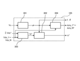
- FIG. 3A is a diagram showing an example of a primary control circuit 105 according to the first embodiment.
- the primary control circuit 105 includes a PLL circuit 301, a current command value planner 302, a voltage controller 303, and a duty allocation planner 304.
- the primary control circuit 105 receives a system voltage detection value Vu detected by a voltage sensor (not shown).
- the system voltage detection value is input to a PLL circuit 301, which detects the amplitude, frequency f, and phase ⁇ of the system voltage. These detection values are input to a current command value planner 302. Furthermore, the frequency f and phase ⁇ are transmitted to each of the secondary control circuits 104_1 to 104_N.
- PLL is an abbreviation for Phase Locked Loop.
- the primary control circuit 105 receives an external input of a total DC voltage command value ⁇ Vdc * of each of the power converter cells 103_1 to 103_N, and receives DC voltage detection values Vdc_1 to Vdc_N detected by voltage sensors 109_1 to 109_N provided in each of the power converter cells 103_1 to 103_N from each of the secondary control circuits 104_1 to 104_N. These values are input to a voltage controller 303, and a grid current amplitude command value Iu * is calculated by, for example, a PID controller provided in the voltage controller 303. Note that P stands for proportional control, I for integral control, and D for differential control.
- the grid current amplitude command value Iu * is input to a current command value planner 302.
- the current command value planner 302 calculates a grid current instantaneous value plan command value iu* for a communication cycle using the input grid current amplitude command value Iu * , the phase ⁇ , and the frequency f, and transmits the calculated grid current instantaneous value plan command value iu * to each of the secondary control circuits 104_1 to 104_N.
- the amplitude, phase ⁇ , and frequency f of the system voltage and the DC voltage detection values Vdc_1 to Vdc_N are input to the duty allocation planner 304. Based on the amplitude, phase ⁇ , and frequency f of the system voltage, the duty allocation plan command values duty_1 * to duty_N * of each of the power converter cells 103_1 to 103_N for the communication period are calculated in the duty allocation planner 304, and transmitted to each of the secondary control circuits 104_1 to 104_N.
- the 3A calculates a current command value (grid current amplitude command value Iu * ) and a duty ratio command value (duty ratio allocation plan command values duty_1 * to duty_N * ) of the grid current for a communication cycle between the primary control circuit 105 and the secondary control circuit 104, and outputs them to the secondary control circuit 104.
- the primary control circuit 105 calculates the current command value (grid current amplitude command value Iu * ) and the duty ratio command values (duty ratio allocation plan command values duty_1 * to duty_N * ) so that one secondary control circuit 104 always enables the current controller 305.
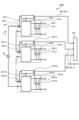
- FIG. 3B is a diagram showing an example of a control block of the secondary control circuit 104 according to embodiment 1. Although FIG. 3 shows the secondary control circuit 104_1, the same applies to each of the secondary control circuits 104_2 to 104_N.
- the secondary control circuit 104 includes a current controller 305, a current control switch 306, a PWM pulse generator 307, and a current instantaneous command value generator 308.
- the secondary control circuit 104_1 provided in the power converter cell 103_1 is shown as an example.
- the other secondary control circuits have the same configuration, so a description thereof will be omitted here.
- the secondary control circuit 104_1 receives the system current instantaneous value plan command value iu * and the duty ratio allocation plan command value duty_1 * output from the primary control circuit 105, the system current detection value iu detected by the current sensor 108_1, the frequency f, and the phase ⁇ .
- the current instantaneous command value generator 308 calculates the system current instantaneous command value iu * ' using the system current instantaneous value planning command value iu * , frequency f, and phase ⁇ , and the system current deviation iuerr is calculated from the system current instantaneous command value iu * ' and the system current detection value iu and inputted to the current controller 305.
- the current control switch 306 receives the grid current deviation iuerr and the duty ratio allocation plan command value duty_1 * . If the duty ratio allocation plan command value duty_1 * is -1, 0, or 1 and the grid current deviation iuerr is less than a predetermined threshold value, the current control switch 306 outputs a current control disable signal to the current controller 305. On the other hand, if the duty ratio allocation plan command value duty_1 * is other than -1, 0, or 1, the current control switch 306 outputs a current control enable signal to the current controller 305.
- the current control switch 306 outputs a current control enable signal to the current controller 305. Details will be described later with reference to FIG. 4.
- the current controller 305 performs calculations, for example, by a PID controller while receiving an effective signal, and calculates the duty ratio control amount ⁇ duty_1 * . While receiving an invalid signal, the calculations by the PID controller are stopped, and the duty ratio control amount ⁇ duty_1 is output as zero. The output duty ratio control amount ⁇ duty_1 is added to the duty ratio allocation plan command value duty_1 * , and input to the PWM pulse generator 307 as the duty ratio output duty_1.
- the PWM pulse generator 307 generates gate signals to drive the switching elements S1 to S4 (see FIG. 2) based on the input duty ratio output duty_1, and inputs these signals to the switching elements S1 to S4 via a gate drive circuit (not shown).
- the secondary control circuit 104 in FIG. 3B determines whether the current controller 305 is enabled or disabled based on the deviation (system current deviation iuerr) between the current command value (system current instantaneous value planning command value iu * ) received from the primary control circuit 105 and the current detection value (system current detection value iu) obtained from the current detection means (current sensor 108), and the duty ratio command value (e.g., duty ratio allocation planning command value duty_1 * ) received from the primary control circuit 105.
- the deviation system current deviation iuerr
- the current command value system current instantaneous value planning command value iu *
- the current detection value system current detection value iu
- the duty ratio command value e.g., duty ratio allocation planning command value duty_1 *
- one of the power converter cells 103_1 to 103_N performs grid current control. This is because the grid current is common to the power converter cells 103_1 to 103_N, and if current control is performed simultaneously, there is a possibility that the current control will become unstable due to detection errors of the current sensors 108_1 to 108_N, etc.
- the other power converter cells are controlled to autonomously start current control. Therefore, this control can stably control the grid current regardless of the communication frequency of the primary control circuit 105 and each of the secondary control circuits 104_1 to 104_N. Therefore, an inexpensive low-speed communication method can be applied, and the power conversion device 100 can be reduced in cost without impairing control stability.
- FIG. 4 is a flowchart showing an example of the control of the current control switch 306 provided in each of the secondary control circuits 104_1 to 104_N according to the first embodiment. Note that the secondary control circuit 104_1 will be described here, and a description of the secondary control circuits 104_2 to 104_N, which have a similar configuration, will be omitted.
- the current control switch 306 starts a series of steps for determining whether to enable or disable the current control (step S401).
- the current control switch 306 determines whether the input duty ratio allocation plan command value duty_1 * is ⁇ 1, 0, or 1 (step S402). If NO in step S402, the current control switch 306 enables the current control (step S406). If the answer is YES in step S402, the current control switch 306 determines whether the absolute value of the grid current deviation iuerr, which is the difference between the grid current instantaneous value planning command value iu * and the grid current detection value iu, is less than a threshold value (step S403). If the answer is YES in step S403, the current control switch 306 disables the current control (step S404).
- step S403 determines whether the duty ratio can be manipulated based on the polarity of the grid current detection value iu and the grid current deviation iuerr, and the duty ratio output duty_1 (step S405). If NO in step S405, the current control switch 306 controls so as to enable the current control during the planning period and disable the current control during the other periods (step S404). If the answer is YES in step S405, the current control switch 306 enables the current control (step S406).
- the planned period is a period planned for control by each power converter cell 103, and corresponds to periods T1, T2, T3, ... in Fig. 5. This completes the series of steps in the flow (step S407).
- the above control flow allows the grid current to be controlled by one power converter cell 103 under normal circumstances, and the grid current to be controlled by multiple power converter cells 103 only when the grid current deviation iuerr is equal to or greater than a threshold value.
- FIG. 5 is a diagram showing an example of each waveform of the power conversion device 100 according to the first embodiment.
- the waveform is extracted during one communication period Tctrl out of one period of the AC system 101, and shows the period during which the system current detection value iu increases from zero in the positive direction when the direction shown in FIG. 1 is taken as positive.
- FIG. 5 also shows the duty ratio outputs duty_1, duty_2, and duty_3 of three power converter cells.
- power converter cell 103_1 performs current control, and the duty ratio outputs duty_2 and duty_3 of power converter cells 103_2 and 103_3 are 0, so no switching occurs and no current control is performed.
- duty_1 reaches the upper limit of 1 at the boundary between periods T1 and T2, from period T2 onwards, power converter cell 103_2 performs current control, setting the duty ratio output duty_1 of power converter cell 103_1 to 1 and duty_3 of power converter cell 103_3 to 0.
- FIG. 5 shows a case in which the system current detection value iu exceeds the system current instantaneous value planning command value iu * during period T2 due to some factor.
- the power converter cell 103_2 controls the grid current, and therefore the duty ratio output duty_2 is increased to suppress the current.
- the duty ratio output duty_2 reaches an upper limit, the grid current cannot be controlled thereafter, and the deviation between the grid current detection value iu and the grid current instantaneous value planned command value iu * , that is, the grid current deviation iuerr, increases.
- the grid current deviation iuerr reaches a threshold value or more, the power converter cell 103_3, which was scheduled to control the grid current in the period T3, autonomously starts current control.
- the grid current detection value iu is again controlled so as to follow the grid current instantaneous value planning command value iu * .
- FIG. 6 is a diagram showing an example of the circuit configuration of a power conversion device 100B according to embodiment 2.
- the primary control circuit 105 and each of the secondary control circuits 104_1 to 104_N are connected by a communication line 601, and are configured in a star topology rather than a daisy chain.
- the primary control circuit 105 and the secondary control circuit 104_1 are connected by a communication line 601_1
- the primary control circuit 105 and the secondary control circuit 104_2 are connected by a communication line 601_2
- the primary control circuit 105 and the secondary control circuit 104_N are connected by a communication line 601_N.
- the configuration of embodiment 2 allows signals to be sent from the primary control circuit 105 to each of the secondary control circuits 104_1 to 104_N simultaneously, and the communication frequency or voltage control frequency can be increased or the dead time of control can be reduced.
- the primary control circuit 105 and each of the secondary control circuits 104_1 to 104_N are connected one-to-one, a dielectric strength voltage equal to or greater than the system voltage of the AC system 101 is required between the primary control circuit 105 and each of the secondary control circuits 104_1 to 104_N.
- the functions of the primary control circuit 105 in the first and second embodiments are provided to each of the secondary control circuits 104_1 to 104_N, and the separately provided primary control circuit 105 is eliminated.
- the differences from the first and second embodiments are described, and the same points as the first and second embodiments are omitted.
- FIG. 7 is a diagram showing an example of a circuit configuration of a power conversion device 100C according to the third embodiment.
- the primary control circuit 105 is omitted.
- the secondary control circuits 104_1 to 104_N are configured as a daisy chain, but the present invention is not limited to this, and may be configured as a star type as shown in the second embodiment, for example.
- a fourth embodiment of the present invention is an application of the power conversion device 100 in the first to third embodiments to a three-phase system.
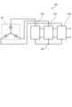
- FIG. 8 shows an example of the configuration of a power conversion device 800 according to the fourth embodiment.
- FIG. 8 shows a three-phase power conversion system in which the power conversion device 100 is connected to each phase of a three-phase system.
- the power conversion devices 100u, 100v, and 100w are connected to the U-phase, V-phase, and W-phase of a three-phase AC system 801 (three-phase system), respectively, and each power conversion device is connected at a neutral point 802.
- the power conversion device 100 By connecting the power conversion device 100 to each phase in this way, it can be used as a three-phase power conversion system.
- the primary control circuit (not shown) contributes to reducing the cost and size of the power conversion device 800 by consolidating it into one instead of dividing it into each power conversion device 100u, 100v, and 100w.
- the three-phase AC system 801 and the power conversion devices 100u, 100v, and 100w are all connected by a Y connection, but this is not limited to this in the present invention, and they may be connected by a delta connection.
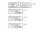
- FIG. 9A is a diagram showing an overview of the control of a power conversion device of the comparative example.
- the main controller 205 is responsible for voltage control and current control
- the sub-controller 204 is responsible for gate signal generation, so control is performed with a communication period (e.g., 100 ⁇ s) that is equal to or shorter than the current control period (calculation period).
- the control of the power converter of this embodiment has the following features.
- FIG. 9B is a diagram showing an overview of the control of the power conversion device of this embodiment.
- the primary control circuit 105 has a voltage control function
- the secondary control circuit 104 has a current control function.
- one secondary control circuit 104 performs current control, and when there is a large deviation between the detected current and the command value, two or more secondary control circuits 104 perform current control.
- current control is possible with a communication cycle of ms. In other words, the communication cycle between the primary control circuit 105 and the secondary control circuit 104 is set longer than the calculation cycle of the current controller 305.
- the multistage circuit includes a primary control circuit 105 having a voltage controller 303 that controls the output voltage of the power converter cells 103, and each power converter cell 103 includes a secondary control circuit 104, and the primary control circuit 105 outputs a command value for the grid current calculated by the voltage controller 303, and the secondary control circuit 104 detects the grid current and can control the grid current based on the command value for the grid current output by the primary control circuit.
- the names primary and secondary are used to refer to the circuit (device) with reference numeral 104 as secondary, but this is not limiting.
- the circuit (device) with reference numeral 104 may be referred to as primary, and the circuit with reference numeral 105 as secondary.
- the multi-stage circuit may have a voltage controller 303 that controls the output voltage of the power converter cells 103 and a secondary control circuit that outputs a command value for the grid current calculated by the voltage controller 303, and each power converter cell 103 may have a primary control circuit that has a current detection means that detects the grid current and a current controller 305 that controls the grid current based on the command value for the grid current output by the secondary control circuit.
Landscapes
- Engineering & Computer Science (AREA)
- Power Engineering (AREA)
- Inverter Devices (AREA)
Abstract
電力変換器セル(103)が複数直列に接続された多段形回路を有する、交流を直流にまたは直流を交流に電力変換する電力変換装置(100)において、多段形回路は、電力変換器セルの出力電圧を制御する電圧制御器(303)を有し、電圧制御器(303)が演算した系統電流の指令値を出力するプライマリ制御回路(105)を備え、電力変換器セル(103)は、系統電流を検出する電流検出手段(108)と、プライマリ制御回路(105)が出力した前記系統電流の指令値に基づき系統電流を制御する電流制御器(305)とを有するセカンダリ制御回路(104)を備える。プライマリ制御回路(105)とセカンダリ制御回路(104)とを接続する通信線は、デイジーチェーン型で結線されている。
Description
本発明は電力変換装置、三相電力変換システムおよびその制御方法に関する。
高圧の交流系統(三相6.6kV系統等)に連系する電力変換装置として、低耐圧のパワーデバイスや受動部品で構成された電力変換器セルを直列接続した構成(直列多段形回路と呼称する)が従来から提案されている(特許文献1参照)。
高圧交流系統の交流電力を直流電力に変換するAC―DCコンバータは、系統電流を要求された力率(例えば力率1)になるように制御するよう要求され、直列多段形回路で系統連系AC―DCコンバータを構成する場合、回路全体で1つのAC―DCコンバータとして振る舞うよう各電力変換器セルを制御する必要がある。
このため、直列多段形回路は、直流電圧制御や系統電流制御等の各制御器を搭載したプライマリ制御回路と、各電力変換器セルが備えるパワーデバイスを駆動するセカンダリ制御回路とで制御されており、プライマリ制御回路とセカンダリ制御回路の間は通信線で接続されることが一般的である。
また、系統電流制御では、高調波抑制対策ガイドラインに準拠して系統電流を商用周波数50Hzもしくは60Hzの正弦波に制御する必要があるため、電流制御器の演算周波数は10kHz以上に設定されることが多い。直列多段形回路の場合、プライマリ制御回路に電流制御器を設け、各電力変換器セルが備えたパワーデバイスのオン時比率(duty比)やゲート信号パターンの指令を、通信線を介してセカンダリ制御回路に送信する必要がある。前述のように電流制御器の演算周波数は概ね10kHz以上であるため、安定した電流制御を行うためには通信周波数も概ね10kHz以上に設定する必要がある。
プライマリ制御回路とセカンダリ制御回路の通信周波数を電流制御器の演算周波数と同等にするためには、高速な通信手法が必要である。一般的に通信速度が高速な通信方式ほど高価であり、電力変換装置の低コスト化のためには安価な低速通信手法を用いることが考えられる。しかしながら、通信周波数を電流制御器の演算周波数未満にすると、電流制御器の出力が各電力変換器セルの操作量に反映されず、特に系統電圧や負荷電力が急変した場合に電流制御が不安定化する可能性がある。したがって、電力変換装置の低コスト化に向けて、安価な低速通信手法を用いた場合における安定した系統電流制御の実現が課題である。
本発明は、前記した課題を解決するためになされたものであり、直列多段形回路の通信系の低コスト化を実現できる電力変換装置、三相電力変換システムおよびその制御方法を提供することを目的とする。
前記目的を達成するため、本発明の電力変換装置は、電力変換器セルが複数直列に接続された多段形回路を有する、交流を直流にまたは直流を交流に電力変換する電力変換装置において、前記多段形回路は、前記電力変換器セルの出力電圧を制御する電圧制御器を有し、前記電圧制御器が演算した系統電流の指令値を出力するプライマリ制御回路を備え、各前記電力変換器セルは、前記系統電流を検出する電流検出手段と、前記プライマリ制御回路が出力した前記系統電流の指令値に基づき前記系統電流を制御する電流制御器とを有するセカンダリ制御回路を備えることを特徴とする。本発明のその他の態様については、後記する実施形態において説明する。
本発明によれば、直列多段形回路の通信系の低コスト化を実現できる。
以下、図面等を用いて、本発明の実施形態について説明する。
<実施形態1>
図1は、実施形態1に係る電力変換装置100の回路構成の一例である。電力変換装置100は、単相の交流系統101を受電し、ACリアクトル102と、複数の電力変換器セル103(第1~第Nの電力変換器セル103)と、電力変換器セル103を駆動するセカンダリ制御回路104(第1~第Nのセカンダリ制御回路104)と、電力変換装置100全体を制御するプライマリ制御回路105とを備える。プライマリ制御回路105とセカンダリ制御回路104は、通信線110でデイジーチェーン型の結線で接続されている。
<実施形態1>
図1は、実施形態1に係る電力変換装置100の回路構成の一例である。電力変換装置100は、単相の交流系統101を受電し、ACリアクトル102と、複数の電力変換器セル103(第1~第Nの電力変換器セル103)と、電力変換器セル103を駆動するセカンダリ制御回路104(第1~第Nのセカンダリ制御回路104)と、電力変換装置100全体を制御するプライマリ制御回路105とを備える。プライマリ制御回路105とセカンダリ制御回路104は、通信線110でデイジーチェーン型の結線で接続されている。
電力変換装置100は、電力変換器セル103が複数直列に接続された多段形回路を有する、交流を直流にまたは直流を交流に電力変換する電力変換装置において、多段形回路は、電力変換器セル103の出力電圧を制御する電圧制御器303(図3A参照)を有し、電圧制御器303が演算した系統電流の指令値を出力するプライマリ制御回路105(プライマリ制御装置)を備え、各前記電力変換器セル103は、系統電流を検出する電流検出手段(電流センサ108)と、プライマリ制御回路が出力した系統電流の指令値に基づき系統電流を制御する電流制御器305(図3B参照)と、を有するセカンダリ制御回路104(セカンダリ制御装置)を備える。
電力変換器セル103は、AC―DCコンバータ106と、直流部に接続された平滑コンデンサ107と、系統電流を検出する電流センサ108と、直流部電圧を検出する電圧センサ109とを備える。
具体的には、電力変換装置100は、電力変換器セル103_1と、電力変換器セル103_1を駆動するセカンダリ制御回路104_1と、電力変換器セル103_1と同様の構成である電力変換器セル103_2から第N(Nは自然数)の電力変換器セル103_Nと、それぞれの電力変換器セル103_2~103_Nを駆動するセカンダリ制御回路104_2~104_Nと、電力変換装置100全体を制御するプライマリ制御回路105とを備える。
各電力変換器セル103_1~103_Nは、AC―DCコンバータ106_1~106_Nと、直流部に接続された平滑コンデンサ107_1~107_Nと、系統電流を検出する電流センサ108_1~108_Nと、直流部電圧を検出する電圧センサ109_1~109_Nとを備える。
プライマリ制御回路105とセカンダリ制御回路104_1は通信線110_1で接続され、さらにセカンダリ制御回路104_1とセカンダリ制御回路104_2が通信線110_2で接続され、プライマリ制御回路105と各セカンダリ制御回路104_1~104_Nはいわゆるデイジーチェーン型の結線で接続される。
直列多段形回路では、交流系統101の電圧が各電力変換器セル103_1~103_Nで分圧されるため、それぞれ電位が異なる。デイジーチェーン型で通信線を結線すると、電位差が小さなセカンダリ制御回路同士を接続できるため、通信線110_1~110_Nの絶縁耐圧を交流系統101の電圧と比較して低くできる。
なお、図1では各電力変換器セル103_1~103_Nに各セカンダリ制御回路104_1~104_Nが含まれていないが(図1中の四角い破線枠参照)、これは説明の都合上別に記載しているためであり、各セカンダリ制御回路104_1~104_Nをそれぞれ対応する各電力変換器セル103_1~103_Nに内蔵しても良い。また、セカンダリ制御回路104_Nとプライマリ制御回路105を通信線で接続するいわゆるリング型の構成としても良い。リング型で構成することで通信線を二重化でき、信頼性の向上を図ることができる。
図2は、実施形態1に係る電力変換器セル103が備えるAC―DCコンバータ106の回路構成の一例を示す図である。AC―DCコンバータ106は、スイッチング素子S1~S4で構成されるフルブリッジ回路から成る。セカンダリ制御回路104とAC―DCコンバータ106は信号線201を介してゲート駆動パターン等の制御信号を送受信する。図1の電力変換器セル103_1~103_Nは、図2の電力変換器セル103と同様の構成であるため説明を省略する。
なお、図2ではスイッチング素子にIGBTを用いているが、本実施形態においてはこれに限定せずMOSFET等の他のスイッチング素子を用いても良い。また、回路方式についてもフルブリッジ回路に限定せず、トーテムポール回路等の他の回路方式を用いても良い。
次に、電力変換装置100の動作を図1および図2を用いて説明する。
各電力変換器セル103_1~103_Nは、全体として一つの単相AC―DCコンバータとして動作する。具体的には、各電力変換器セル103_1~103_Nの直流電圧を所定値に制御しつつ、交流系統101の系統電流を正弦波状に制御する。
各電力変換器セル103_1~103_Nは、全体として一つの単相AC―DCコンバータとして動作する。具体的には、各電力変換器セル103_1~103_Nの直流電圧を所定値に制御しつつ、交流系統101の系統電流を正弦波状に制御する。
各電力変換器セル103_1~103_Nは、各スイッチング素子S1~S4のduty比を操作することでフルブリッジ回路の交流系統側端子間に任意電圧(直流電圧にduty比を掛けた平均電圧)を出力でき、すなわちACリアクトル102に印加される電圧を操作することで系統電流を制御する。
また、本実施形態では詳細を省略するが、各電力変換器セル103_1~103_Nの直流電圧をバランスさせる電圧バランス制御を設けても良く、本実施形態は電圧バランス制御の有無にかかわらず適用可能である。その他、本実施形態で説明していない任意の制御手法を適用しても本発明においては差し支えない。
図3Aは、実施形態1に係るプライマリ制御回路105の一例を示す図である。プライマリ制御回路105は、PLL回路301、電流指令値計画器302、電圧制御器303、duty割当計画器304を含んで構成されている。
プライマリ制御回路105には、不図示の電圧センサで検出された系統電圧検出値Vuが入力される。系統電圧検出値はPLL回路301に入力され、系統電圧の振幅、周波数f、位相θが検出される。これらの検出値は電流指令値計画器302に入力される。さらに、周波数fおよび位相θは各セカンダリ制御回路104_1~104_Nに送信される。なお、PLLはPhase Locked Loopの略称である。
また、プライマリ制御回路105には、外部から各電力変換器セル103_1~103_Nの合計直流電圧指令値ΣVdc*が入力され、各セカンダリ制御回路104_1~104_Nから各電力変換器セル103_1~103_Nが備える電圧センサ109_1~109_Nが検出した直流電圧検出値Vdc_1~Vdc_Nが入力される。これらの値は電圧制御器303に入力され、電圧制御器303が備える例えばPID制御器によって系統電流振幅指令値Iu*が計算される。なお、Pは比例制御,Iは積分制御,Dは微分制御を意味する。
系統電流振幅指令値Iu*は電流指令値計画器302に入力される。電流指令値計画器302では、入力された系統電流振幅指令値Iu*と位相θ・周波数fとを用いて通信周期分の系統電流瞬時値計画指令値iu*が計算され、各セカンダリ制御回路104_1~104_Nに送信される。
duty割当計画器304には、系統電圧の振幅、位相θ、周波数fと、直流電圧検出値Vdc_1~Vdc_Nが入力される。duty割当計画器304では、系統電圧の振幅、位相θ、周波数fに基づき、通信周期分の各電力変換器セル103_1~103_Nの各duty比割当計画指令値duty_1*~duty_N*が計算され、各セカンダリ制御回路104_1~104_Nに送信される。
すなわち、図3Aのプライマリ制御回路105は、プライマリ制御回路105とセカンダリ制御回路104との通信周期分の系統電流の電流指令値(系統電流振幅指令値Iu*)とduty比指令値(duty比割当計画指令値duty_1*~duty_N*)を計算し、セカンダリ制御回路104に出力する。プライマリ制御回路105は、常に1つのセカンダリ制御回路104が電流制御器305を有効にするように電流指令値(系統電流振幅指令値Iu*)とduty比指令値(duty比割当計画指令値duty_1*~duty_N*)を計算する。
図3Bは、実施形態1に係るセカンダリ制御回路104の制御ブロックの一例を示す図である。図3では、セカンダリ制御回路104_1について示しているが、各セカンダリ制御回路104_2~104_Nについても同様である。
セカンダリ制御回路104は、電流制御器305、電流制御切替器306、PWMパルス生成器307、電流瞬時指令値生成器308を含んで構成される。図3では例として電力変換器セル103_1が備えるセカンダリ制御回路104_1を示している。他のセカンダリ制御回路も同様の構成であるため、ここでは説明を省略する。
セカンダリ制御回路104_1にはプライマリ制御回路105から出力された系統電流瞬時値計画指令値iu*とduty比割当計画指令値duty_1*、電流センサ108_1が検出した系統電流検出値iu、周波数f、位相θが入力される。
セカンダリ制御回路104_1では、電流瞬時指令値生成器308で系統電流瞬時値計画指令値iu*、周波数f、位相θを用いて系統電流瞬時指令値iu*’が計算され、系統電流瞬時指令値iu*’と系統電流検出値iuから系統電流偏差iuerrが計算され、電流制御器305に入力される。
電流制御切替器306には、系統電流偏差iuerrとduty比割当計画指令値duty_1*が入力される。電流制御切替器306は、duty比割当計画指令値duty_1*が-1、0、1であり、かつ系統電流偏差iuerrが所定のしきい値未満であれば電流制御の無効信号を電流制御器305に出力する。一方、duty比割当計画指令値duty_1*が-1、0、1以外の場合は電流制御の有効信号を電流制御器305に出力する。さらに、duty比割当計画指令値duty_1*が-1、0、1であり、かつ系統電流偏差iuerrが所定のしきい値以上であれば電流制御の有効信号を電流制御器305に出力する。詳細は図4で後述する。
電流制御器305は、有効信号を受信している間は、例えばPID制御器による演算を行い、duty比操作量Δduty_1*を計算する。無効信号を受信している間はPID制御器による演算を停止し、duty比操作量Δduty_1をゼロとして出力する。出力されたduty比操作量Δduty_1はduty比割当計画指令値duty_1*と合算されduty比出力duty_1としてPWMパルス生成器307に入力される。
PWMパルス生成器307では、入力されたduty比出力duty_1に基づき、スイッチング素子S1~S4(図2参照)を駆動するゲート信号を生成し、不図示のゲートドライブ回路を介してスイッチング素子S1~S4に入力される。
すなわち、図3Bのセカンダリ制御回路104は、プライマリ制御回路105から受信した電流指令値(系統電流瞬時値計画指令値iu*)と電流検出手段(電流センサ108)から得られた電流検出値(系統電流検出値iu)との偏差(系統電流偏差iuerr)と、プライマリ制御回路105から受信したduty比指令値(例えば、duty比割当計画指令値duty_1*)に基づいて、電流制御器305の有効または無効を判定する。
以上の構成により、系統電流瞬時値計画指令値iu*と系統電流検出値iuがほぼ一致している通常時は、各電力変換器セル103_1~103_Nのうち1つの電力変換器セルが系統電流制御を行う。これは、系統電流が各電力変換器セル103_1~103_Nで共通であり、同時に電流制御を行うと、電流センサ108_1~108_Nの検出誤差等に起因して電流制御が不安定化する可能性があるためである。
一方、系統電圧や負荷電力の急変等により、その時刻に系統電流制御していた電力変換器セルのduty比出力が上下限値に張り付き、系統電流瞬時値計画指令値iu*と系統電流検出値iuが乖離する非常時においては、他の電力変換器セルが自律的に電流制御を開始するように制御する。このため、本制御は、プライマリ制御回路105と各セカンダリ制御回路104_1~104_Nの通信周波数によらずに系統電流を安定に制御できる。したがって、安価な低速通信方式を適用できるようになり、電力変換装置100は制御安定性を損なわずに低コスト化ができる。
図4は、実施形態1に係る各セカンダリ制御回路104_1~104_Nが備える電流制御切替器306の制御の一例を示すフローチャートである。なお、ここではセカンダリ制御回路104_1について説明し、同様の構成であるセカンダリ制御回路104_2~104_Nについては説明を省略する。
電流制御切替器306は、電流制御を有効とするか無効とするかを判定する一連のフローが開始する(ステップS401)。
電流制御切替器306は、入力されたduty比割当計画指令値duty_1*が、-1、0、1かどうか判定する(ステップS402)。
ステップS402でNOの場合、電流制御切替器306は、電流制御を有効とする(ステップS406)。
ステップS402でYESの場合、電流制御切替器306は、系統電流瞬時値計画指令値iu*と系統電流検出値iuの差分である系統電流偏差iuerrの絶対値がしきい値未満かどうか判定する(ステップS403)。
ステップS403でYESの場合、電流制御切替器306は、電流制御を無効とする。(ステップS404)
電流制御切替器306は、入力されたduty比割当計画指令値duty_1*が、-1、0、1かどうか判定する(ステップS402)。
ステップS402でNOの場合、電流制御切替器306は、電流制御を有効とする(ステップS406)。
ステップS402でYESの場合、電流制御切替器306は、系統電流瞬時値計画指令値iu*と系統電流検出値iuの差分である系統電流偏差iuerrの絶対値がしきい値未満かどうか判定する(ステップS403)。
ステップS403でYESの場合、電流制御切替器306は、電流制御を無効とする。(ステップS404)
ステップS403でNOの場合、電流制御切替器306は、系統電流検出値iuと系統電流偏差iuerrの極性およびduty比出力duty_1に基づき、duty比を操作可能か判定する(ステップS405)。
ステップS405でNOの場合、電流制御切替器306は、計画期間に電流制御を有効とし、それ以外の期間では電流制御を無効とするように制御する(ステップS404)。
ステップS405でYESの場合、電流制御切替器306は、電流制御を有効とする(ステップS406)。なお、計画期間とは、各電力変換器セル103が制御するために計画された期間であり、図5の期間T1,T2,T3,・・・に対応する。
以上で一連のフローが終了する(ステップS407)。
ステップS405でNOの場合、電流制御切替器306は、計画期間に電流制御を有効とし、それ以外の期間では電流制御を無効とするように制御する(ステップS404)。
ステップS405でYESの場合、電流制御切替器306は、電流制御を有効とする(ステップS406)。なお、計画期間とは、各電力変換器セル103が制御するために計画された期間であり、図5の期間T1,T2,T3,・・・に対応する。
以上で一連のフローが終了する(ステップS407)。
以上の制御フローにより、通常時は1つの電力変換器セル103で系統電流を制御し、系統電流偏差iuerrがしきい値以上となった場合にのみ複数台の電力変換器セル103で系統電流制御することができる。
図5は、実施形態1に係る電力変換装置100の各波形の一例を示す図である。交流系統101の1周期のうち1通信周期Tctrlにおける波形を抜き出したものであり、系統電流検出値iuが図1に示した向きを正とした場合において、ゼロから正の方向に増加する期間を示している。また、図5には、電力変換器セル3台分のduty比出力duty_1,duty_2,duty_3を示している。
期間T1では、電力変換器セル103_1が電流制御を行い、電力変換器セル103_2,103_3のduty比出力duty_2,duty_3は0のためスイッチングせず電流制御していない。
期間T1と期間T2の境界でduty_1が上限の1に達するため、期間T2からは電力変換器セル103_2が電流制御を行い、電力変換器セル103_1のduty比出力duty_1を1、電力変換器セル103_3のduty_3を0とする。
この時、通常であれば期間T2においても期間T1と同様に常に1つの電力変換器セルが電流制御を行うが、図5では期間T2において、何等かの要因により系統電流検出値iuが系統電流瞬時値計画指令値iu*を超過してしまうケースを示している。
期間T2では、電力変換器セル103_2が系統電流制御しているため、電流を抑制するようにduty比出力duty_2を高くする方向に操作する。しかしながら、duty比出力duty_2が上限に達してしまうと、その後は系統電流制御できないため系統電流検出値iuと系統電流瞬時値計画指令値iu*の偏差、すなわち系統電流偏差iuerrが増大する。系統電流偏差iuerrがしきい値以上になると、期間T3で系統電流制御を行う計画であった電力変換器セル103_3が自律的に電流制御を開始する。
すなわち、電流指令値とセカンダリ制御回路104の電流検出手段から得られた電流検出値との偏差が所定値以上の場合、2つ以上の前記セカンダリ制御回路104が各々の電流制御器305を有効にする。
これにより、系統電流検出値iuが再び系統電流瞬時値計画指令値iu*に追従して制御されるようになる。以上の制御により、プライマリ制御回路105からの通信が無い状態でも安定した系統電流制御を実現できる。
<実施形態2>
本発明の実施形態2は、実施形態1におけるプライマリ制御回路105と各セカンダリ制御回路104_1~104_Nとの通信線をいわゆるスター型で接続したものである。以下では、実施形態1との差分について述べ、実施形態1と同様である点については説明を省略する。
本発明の実施形態2は、実施形態1におけるプライマリ制御回路105と各セカンダリ制御回路104_1~104_Nとの通信線をいわゆるスター型で接続したものである。以下では、実施形態1との差分について述べ、実施形態1と同様である点については説明を省略する。
図6は、実施形態2に係る電力変換装置100Bの回路構成の一例を示す図である。実施形態2では、プライマリ制御回路105と各セカンダリ制御回路104_1~104_Nとは通信線601で接続され、デイジーチェーンではなく、スター型で構成したものである。
具体的には、プライマリ制御回路105とセカンダリ制御回路104_1は、通信線601_1で接続され、プライマリ制御回路105とセカンダリ制御回路104_2は、通信線601_2で接続され、プライマリ制御回路105とセカンダリ制御回路104_Nは、通信線601_Nで接続されている。
このため、実施形態2の構成は、プライマリ制御回路105から同時に各セカンダリ制御回路104_1~104_Nへ信号を送信でき、通信周波数や電圧制御周波数を高める、もしくは制御のむだ時間を削減できる。ただし、プライマリ制御回路105と各セカンダリ制御回路104_1~104_Nが一対一で接続されるため、プライマリ制御回路105と各セカンダリ制御回路104_1~104_N間は、交流系統101の系統電圧以上の絶縁耐圧が必要となる。
<実施形態3>
実施形態3は、実施形態1および実施形態2おけるプライマリ制御回路105の機能を各セカンダリ制御回路104_1~104_Nに持たせ、別置きのプライマリ制御回路105を削除したものである。以下では、実施形態1および実施形態2との差分について述べ、実施形態1および実施形態2と同様である点については説明を省略する。
実施形態3は、実施形態1および実施形態2おけるプライマリ制御回路105の機能を各セカンダリ制御回路104_1~104_Nに持たせ、別置きのプライマリ制御回路105を削除したものである。以下では、実施形態1および実施形態2との差分について述べ、実施形態1および実施形態2と同様である点については説明を省略する。
図7は、実施形態3に係る電力変換装置100Cの回路構成の一例を示す図である。実施形態3では、プライマリ制御回路105が削除された構成になっている。各セカンダリ制御回路104_1~104_Nの少なくとも1つにプライマリ制御回路105の機能を持たせることで、プライマリ制御回路105専用の筐体を用意する必要がなく、電力変換装置100を小型化できる。また、各セカンダリ制御回路104_1~104_Nのうち、2つ以上にプライマリ制御回路105の機能を持たせることで、プライマリとして動作しているセカンダリ制御回路が故障等の理由で停止した場合でも、他のセカンダリ制御回路がプライマリとし動作することで、電力変換装置100の運転を継続でき、信頼性を向上できる。なお、図7では各セカンダリ制御回路104_1~104_N間の通信線をデイジーチェーンで構成しているが、本発明においてはこれに限定せず、例えば実施形態2で示したようなスター型で構成しても良い。
<実施形態4>
本発明の実施形態4は、実施形態1~3における電力変換装置100を三相システムに適用したものである。
本発明の実施形態4は、実施形態1~3における電力変換装置100を三相システムに適用したものである。
図8は、実施形態4に係る電力変換装置800の構成の一例を示したものである。図8には、電力変換装置100を三相系統の各相にそれぞれ接続した三相電力変換システムを示す。三相交流系統801(三相系統)のU相、V相、W相に対してそれぞれ電力変換装置100u,100v,100wが接続されており、各電力変換装置間は中性点802で接続された構成である。このように各相に対して電力変換装置100を接続することで三相電力変換システムとして使用することができる。また、不図示のプライマリ制御回路は、各電力変換装置100u,100v,100wに分けず1つに集約することで電力変換装置800の低コスト化や小型化に寄与する。なお、図8では三相交流系統801および電力変換装置100u,100v,100wはいずれもY結線で接続されているが、本発明においてはこれに限定せず、デルタ結線で接続しても良い。
図9Aは、比較例の電力変換装置の制御の概要を示す図である。比較例の電力変換装置の場合メイン制御器205が電圧制御と電流制御を担当し、サブ制御器204は、ゲート信号生成を担当するため、電流制御周期(演算周期)以下の通信周期(例えば、100μs)で制御していた。これに対し、本実施形態の電力変換器の制御は次の特徴を有する。
図9Bは、本実施形態の電力変換装置の制御の概要を示す図である。プライマリ制御回路105が電圧制御の機能を有し、セカンダリ制御回路104が電流制御機能を有する。通常ひとつのセカンダリ制御回路104が電流制御を行い、検出電流と指令値の偏差が大きい場合は、2つ以上のセカンダリ制御回路104が電流制御をする。本実施形態の制御方式を採用すれば、msオードの通信周期で電流制御が可能となる。すなわち、プライマリ制御回路105とセカンダリ制御回路104との通信周期は、電流制御器305の演算周期よりも長く設定されている。また、直列多段形回路の通信系の低コスト化が実現できる。
本実施形態においては、電力変換器セル103が複数直列に接続された多段形回路を有する、交流を直流にまたは直流を交流に電力変換する電力変換装置の制御方法において、多段形回路は、電力変換器セル103の出力電圧を制御する電圧制御器303を有するプライマリ制御回路105と、各電力変換器セル103はセカンダリ制御回路104を備え、プライマリ制御回路105は、電圧制御器303が演算した系統電流の指令値を出力し、セカンダリ制御回路104は、系統電流を検出し、プライマリ制御回路が出力した前記系統電流の指令値に基づき系統電流を制御することができる。
なお、本実施形態で使用しているプライマリとセカンダリのいう名称について、符号104の回路(装置)をセカンダリと称したがこれに限定するわけではない。符号104の回路(装置)をプライマリと称し、符号105をセカンダリと称してもよい。
すなわち、電力変換器セル103が複数直列に接続された多段形回路を有する、交流を直流にまたは直流を交流に電力変換する電力変換装置において、多段形回路は、電力変換器セル103の出力電圧を制御する電圧制御器303を有し、電圧制御器303が演算した系統電流の指令値を出力するセカンダリ制御回路を備え、各電力変換器セル103は、系統電流を検出する電流検出手段と、セカンダリ制御回路が出力した系統電流の指令値に基づき系統電流を制御する電流制御器305とを有するプライマリ制御回路を備えるとしてもよい。
100 電力変換装置
101 交流系統
102 ACリアクトル
103 電力変換器セル
104 セカンダリ制御回路(セカンダリ制御装置)
105 プライマリ制御回路(プライマリ制御装置)
106 AC―DCコンバータ
107 平滑コンデンサ
108 電流センサ(電流検出手段)
109 電圧センサ
110 通信線
201 信号線
301 PLL回路
302 電流指令値計画器
303 電圧制御器
304 duty割当計画器
305 電流制御器
306 電流制御切替器
307 PWMパルス生成器
308 電流瞬時指令値生成器
601 通信線
duty_1*~duty_N* 各duty比割当計画指令値(duty比指令値)
duty_1 duty比出力
Δduty_1* duty比操作量
iu 系統電流検出値(電流検出値)
iu* 通信周期分の系統電流瞬時値計画指令値(電流指令値)
iu*’ 系統電流瞬時指令値
Iu* 系統電流振幅指令値
iuerr 系統電流偏差(偏差)
f 周波数
θ 位相
S1~S4 スイッチング素子
ΣVdc* 合計直流電圧指令値
Vdc_1~Vdc_N 直流電圧検出値
101 交流系統
102 ACリアクトル
103 電力変換器セル
104 セカンダリ制御回路(セカンダリ制御装置)
105 プライマリ制御回路(プライマリ制御装置)
106 AC―DCコンバータ
107 平滑コンデンサ
108 電流センサ(電流検出手段)
109 電圧センサ
110 通信線
201 信号線
301 PLL回路
302 電流指令値計画器
303 電圧制御器
304 duty割当計画器
305 電流制御器
306 電流制御切替器
307 PWMパルス生成器
308 電流瞬時指令値生成器
601 通信線
duty_1*~duty_N* 各duty比割当計画指令値(duty比指令値)
duty_1 duty比出力
Δduty_1* duty比操作量
iu 系統電流検出値(電流検出値)
iu* 通信周期分の系統電流瞬時値計画指令値(電流指令値)
iu*’ 系統電流瞬時指令値
Iu* 系統電流振幅指令値
iuerr 系統電流偏差(偏差)
f 周波数
θ 位相
S1~S4 スイッチング素子
ΣVdc* 合計直流電圧指令値
Vdc_1~Vdc_N 直流電圧検出値
Claims (13)
- 電力変換器セルが複数直列に接続された多段形回路を有する、交流を直流にまたは直流を交流に電力変換する電力変換装置において、
前記多段形回路は、前記電力変換器セルの出力電圧を制御する電圧制御器を有し、前記電圧制御器が演算した系統電流の指令値を出力するプライマリ制御回路を備え、
各前記電力変換器セルは、前記系統電流を検出する電流検出手段と、前記プライマリ制御回路が出力した前記系統電流の指令値に基づき前記系統電流を制御する電流制御器とを有するセカンダリ制御回路を備える
ことを特徴とする電力変換装置。 - 前記プライマリ制御回路は、前記プライマリ制御回路と前記セカンダリ制御回路との通信周期分の前記系統電流の電流指令値とduty比指令値を計算し、前記セカンダリ制御回路に出力する
ことを特徴とする請求項1に記載の電力変換装置。 - 前記プライマリ制御回路は、常に1つの前記セカンダリ制御回路が前記電流制御器を有効にするように前記電流指令値と前記duty比指令値を計算する
ことを特徴とする請求項2に記載の電力変換装置。 - 前記電流指令値と前記セカンダリ制御回路の前記電流検出手段から得られた電流検出値との偏差が所定値以上の場合、2つ以上の前記セカンダリ制御回路が各々の前記電流制御器を有効にする
ことを特徴とする請求項2または請求項3に記載の電力変換装置。 - 前記セカンダリ制御回路は、前記プライマリ制御回路から受信した前記電流指令値と前記電流検出手段から得られた電流検出値の偏差と、前記プライマリ制御回路から受信した前記duty比指令値に基づいて、前記電流制御器の有効または無効を判定する
ことを特徴とする請求項4に記載の電力変換装置。 - 前記プライマリ制御回路と前記セカンダリ制御回路とを接続する通信線は、デイジーチェーン型で結線されている
ことを特徴とする請求項1に記載の電力変換装置。 - 前記プライマリ制御回路と前記セカンダリ制御回路とを接続する通信線は、スター型で結線されている
ことを特徴とする請求項1に記載の電力変換装置。 - 前記プライマリ制御回路と前記セカンダリ制御回路との通信周期は、前記電流制御器の演算周期よりも長く設定されている
ことを特徴とする請求項1に記載の電力変換装置。 - 少なくとも1つの前記セカンダリ制御回路が、前記プライマリ制御回路が有する機能を併せ持つことを特徴とする請求項1に記載の電力変換装置。
- 請求項1乃至3、6乃至9のいずれか1項に記載の電力変換装置を三相系統の各相にそれぞれ接続したことを特徴とする三相電力変換システム。
- 請求項4に記載の電力変換装置を三相系統の各相にそれぞれ接続したことを特徴とする三相電力変換システム。
- 請求項5に記載の電力変換装置を三相系統の各相にそれぞれ接続したことを特徴とする三相電力変換システム。
- 電力変換器セルが複数直列に接続された多段形回路を有する、交流を直流にまたは直流を交流に電力変換する電力変換装置の制御方法において、
前記多段形回路は、前記電力変換器セルの出力電圧を制御する電圧制御器を有するプライマリ制御回路と、各前記電力変換器セルはセカンダリ制御回路を備え、
前記プライマリ制御回路は、前記電圧制御器が演算した系統電流の指令値を出力し、
前記セカンダリ制御回路は、前記系統電流を検出し、前記プライマリ制御回路が出力した前記系統電流の指令値に基づき前記系統電流を制御する
ことを特徴とする電力変換装置の制御方法。
Priority Applications (1)
| Application Number | Priority Date | Filing Date | Title |
|---|---|---|---|
| DE112024001667.7T DE112024001667T5 (de) | 2023-06-27 | 2024-04-24 | Leistungsumwandlungsvorrichtung, dreiphasiges leistungsumwandlungssystem und steuerungsverfahren dafür |
Applications Claiming Priority (2)
| Application Number | Priority Date | Filing Date | Title |
|---|---|---|---|
| JP2023104793A JP2025004905A (ja) | 2023-06-27 | 2023-06-27 | 電力変換装置、三相電力変換システムおよびその制御方法 |
| JP2023-104793 | 2023-06-27 |
Publications (1)
| Publication Number | Publication Date |
|---|---|
| WO2025004513A1 true WO2025004513A1 (ja) | 2025-01-02 |
Family
ID=93938272
Family Applications (1)
| Application Number | Title | Priority Date | Filing Date |
|---|---|---|---|
| PCT/JP2024/016013 Ceased WO2025004513A1 (ja) | 2023-06-27 | 2024-04-24 | 電力変換装置、三相電力変換システムおよびその制御方法 |
Country Status (3)
| Country | Link |
|---|---|
| JP (1) | JP2025004905A (ja) |
| DE (1) | DE112024001667T5 (ja) |
| WO (1) | WO2025004513A1 (ja) |
Citations (7)
| Publication number | Priority date | Publication date | Assignee | Title |
|---|---|---|---|---|
| JPH0731150A (ja) * | 1993-07-09 | 1995-01-31 | Shindengen Electric Mfg Co Ltd | スイッチング電源装置 |
| JP2007200063A (ja) * | 2006-01-27 | 2007-08-09 | Yaskawa Electric Corp | サーボシステム |
| US20140153294A1 (en) * | 2012-12-05 | 2014-06-05 | Infineon Technologies Austria Ag | AC/DC Power Converter Arrangement |
| JP2015130746A (ja) * | 2014-01-07 | 2015-07-16 | 株式会社日立製作所 | 電力変換装置およびその制御方法 |
| US20160079881A1 (en) * | 2014-09-17 | 2016-03-17 | Delta Electronics, Inc. | Power supply and method of supplying power |
| JP2016046959A (ja) * | 2014-08-26 | 2016-04-04 | 富士電機株式会社 | 直流電源装置 |
| JP2019041512A (ja) * | 2017-08-25 | 2019-03-14 | 富士電機株式会社 | 電力変換装置 |
-
2023
- 2023-06-27 JP JP2023104793A patent/JP2025004905A/ja active Pending
-
2024
- 2024-04-24 DE DE112024001667.7T patent/DE112024001667T5/de active Pending
- 2024-04-24 WO PCT/JP2024/016013 patent/WO2025004513A1/ja not_active Ceased
Patent Citations (7)
| Publication number | Priority date | Publication date | Assignee | Title |
|---|---|---|---|---|
| JPH0731150A (ja) * | 1993-07-09 | 1995-01-31 | Shindengen Electric Mfg Co Ltd | スイッチング電源装置 |
| JP2007200063A (ja) * | 2006-01-27 | 2007-08-09 | Yaskawa Electric Corp | サーボシステム |
| US20140153294A1 (en) * | 2012-12-05 | 2014-06-05 | Infineon Technologies Austria Ag | AC/DC Power Converter Arrangement |
| JP2015130746A (ja) * | 2014-01-07 | 2015-07-16 | 株式会社日立製作所 | 電力変換装置およびその制御方法 |
| JP2016046959A (ja) * | 2014-08-26 | 2016-04-04 | 富士電機株式会社 | 直流電源装置 |
| US20160079881A1 (en) * | 2014-09-17 | 2016-03-17 | Delta Electronics, Inc. | Power supply and method of supplying power |
| JP2019041512A (ja) * | 2017-08-25 | 2019-03-14 | 富士電機株式会社 | 電力変換装置 |
Also Published As
| Publication number | Publication date |
|---|---|
| DE112024001667T5 (de) | 2026-02-19 |
| JP2025004905A (ja) | 2025-01-16 |
Similar Documents
| Publication | Publication Date | Title |
|---|---|---|
| EP2722978B1 (en) | System and method for common-mode elimination in a multi-level converter | |
| KR101189993B1 (ko) | 이중화된 구동부를 가진 멀티 레벨 인버터 | |
| CN101814851B (zh) | Pwm整流器 | |
| JP5223711B2 (ja) | 無停電電源装置 | |
| JP6336236B1 (ja) | 電力変換装置 | |
| WO2010082265A1 (ja) | 電力変換装置 | |
| KR101025647B1 (ko) | 고압 인버터의 제어장치 및 방법 | |
| JP2013118743A (ja) | 並列インバータ装置 | |
| JP5950177B2 (ja) | 並列インバータ装置 | |
| JP6864116B2 (ja) | 電力変換システム | |
| WO2021028975A1 (ja) | 電力変換装置 | |
| JP4011534B2 (ja) | 多重変換器で構成される直流送電設備及びその運転方法 | |
| KR101465973B1 (ko) | 멀티레벨 인버터를 적용한 연료전지용 전력변환장치 및 중성점 전위 불평형 저감 방법 | |
| EP1655828A1 (en) | Controller for a wound-rotor induction motor | |
| JP2007274825A (ja) | 電力変換装置 | |
| JP2025004905A (ja) | 電力変換装置、三相電力変換システムおよびその制御方法 | |
| JP4178331B2 (ja) | 直列多重パルス幅変調サイクロコンバータ装置およびその制御方法 | |
| JP5805059B2 (ja) | 電力変換装置 | |
| JP5447400B2 (ja) | モータ駆動装置、モータ駆動システム | |
| JP4783174B2 (ja) | 電力変換装置 | |
| JP4065727B2 (ja) | 多重pwmサイクロコンバータ | |
| JP4755504B2 (ja) | 電力変換装置 | |
| WO2012120703A1 (ja) | 電力送電装置 | |
| JP2021016261A (ja) | 電力変換装置 | |
| JP6690880B2 (ja) | 電力変換装置 |
Legal Events
| Date | Code | Title | Description |
|---|---|---|---|
| 121 | Ep: the epo has been informed by wipo that ep was designated in this application |
Ref document number: 24831388 Country of ref document: EP Kind code of ref document: A1 |
|
| WWE | Wipo information: entry into national phase |
Ref document number: 112024001667 Country of ref document: DE |
|
| WWE | Wipo information: entry into national phase |
Ref document number: 202617004317 Country of ref document: IN |
|
| WWP | Wipo information: published in national office |
Ref document number: 112024001667 Country of ref document: DE |