WO2025004473A1 - モジュール - Google Patents
モジュール Download PDFInfo
- Publication number
- WO2025004473A1 WO2025004473A1 PCT/JP2024/011375 JP2024011375W WO2025004473A1 WO 2025004473 A1 WO2025004473 A1 WO 2025004473A1 JP 2024011375 W JP2024011375 W JP 2024011375W WO 2025004473 A1 WO2025004473 A1 WO 2025004473A1
- Authority
- WO
- WIPO (PCT)
- Prior art keywords
- main surface
- semiconductor component
- groove
- module
- sealing resin
- Prior art date
- Legal status (The legal status is an assumption and is not a legal conclusion. Google has not performed a legal analysis and makes no representation as to the accuracy of the status listed.)
- Ceased
Links
Images



Classifications
-
- H—ELECTRICITY
- H05—ELECTRIC TECHNIQUES NOT OTHERWISE PROVIDED FOR
- H05K—PRINTED CIRCUITS; CASINGS OR CONSTRUCTIONAL DETAILS OF ELECTRIC APPARATUS; MANUFACTURE OF ASSEMBLAGES OF ELECTRICAL COMPONENTS
- H05K1/00—Printed circuits
- H05K1/18—Printed circuits structurally associated with non-printed electric components
-
- H—ELECTRICITY
- H10—SEMICONDUCTOR DEVICES; ELECTRIC SOLID-STATE DEVICES NOT OTHERWISE PROVIDED FOR
- H10W—GENERIC PACKAGES, INTERCONNECTIONS, CONNECTORS OR OTHER CONSTRUCTIONAL DETAILS OF DEVICES COVERED BY CLASS H10
- H10W74/00—Encapsulations, e.g. protective coatings
- H10W74/10—Encapsulations, e.g. protective coatings characterised by their shape or disposition
-
- H—ELECTRICITY
- H10—SEMICONDUCTOR DEVICES; ELECTRIC SOLID-STATE DEVICES NOT OTHERWISE PROVIDED FOR
- H10W—GENERIC PACKAGES, INTERCONNECTIONS, CONNECTORS OR OTHER CONSTRUCTIONAL DETAILS OF DEVICES COVERED BY CLASS H10
- H10W74/00—Encapsulations, e.g. protective coatings
- H10W74/40—Encapsulations, e.g. protective coatings characterised by their materials
-
- H—ELECTRICITY
- H10—SEMICONDUCTOR DEVICES; ELECTRIC SOLID-STATE DEVICES NOT OTHERWISE PROVIDED FOR
- H10W—GENERIC PACKAGES, INTERCONNECTIONS, CONNECTORS OR OTHER CONSTRUCTIONAL DETAILS OF DEVICES COVERED BY CLASS H10
- H10W90/00—Package configurations
Definitions
- the present invention relates to a module.
- Patent Document 1 JP 2021-197568 A
- a groove is formed in the sealing resin near the side of the mounted component.
- the groove is intended to relieve stress or prevent electromagnetic interference.
- the effect of bending stress is largely influenced by the difference in linear expansion coefficient between the sealing resin below the mounted component and the board.
- the mounted component is large, simply providing a groove near the side of the component is insufficient to deal with stress.
- the present invention aims to provide a module that can reduce bending stress even when the size of the semiconductor components mounted on the board is large.
- the module according to the present invention comprises a substrate having a main surface, a semiconductor component mounted on the main surface, and an encapsulating resin layer formed of encapsulating resin so as to encapsulate the main surface and the side surface of the semiconductor component, the semiconductor component comprising a component body and bumps connected to the surface of the component body facing the substrate.
- the semiconductor component is mounted on the main surface by connecting the bumps to the main surface while the component body is spaced from the main surface.
- An underfill layer is formed by filling the gap between the component body and the main surface with underfill resin.
- the elastic modulus of the underfill resin is lower than the elastic modulus of the encapsulating resin.
- the underfill layer includes a protruding portion that exists outside the area where the component body is projected onto the main surface.
- the protruding portion is covered by the encapsulating resin layer.
- a groove is formed in the encapsulating resin layer within the area where the protruding portion is projected onto the surface of the encapsulating resin layer farther from the substrate.
- the stress caused by the difference in linear expansion coefficient between the semiconductor component and the substrate is alleviated by the underfill layer, and further, the stress caused by the difference in linear expansion coefficient between the sealing resin layer and the semiconductor component is alleviated by the groove, so that even if the size of the semiconductor component mounted on the substrate is large, the stress caused by bending can be alleviated.
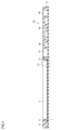
- FIG. 1 is a cross-sectional view of a module in a first embodiment according to the present invention.
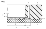
- FIG. 2 is an enlarged view of a portion Z1 in FIG. 1 is a plan view of a module in a first embodiment according to the present invention.
- 4 is an enlarged view of the bottom of a groove of a module and its vicinity in the first embodiment according to the present invention.
- FIG. 13 is an enlarged view of the bottom of a groove and its vicinity in a first modified example of the module in the first embodiment based on the present invention.
- FIG. 13 is an enlarged view of the bottom of a groove and its vicinity in a second modified example of the module in the first embodiment based on the present invention.
- FIG. 11 is a plan view of a module in a second embodiment according to the present invention.
- FIG. 11 is a plan view of a module in a third embodiment according to the present invention.
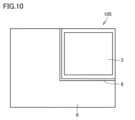
- FIG. 13 is a plan view of a first modified example of the module in the third embodiment according to the present invention.
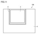
- FIG. 13 is a plan view of a second modified example of the module in the third embodiment according to the present invention.
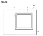
- FIG. 13 is a plan view of a third modified example of the module in the third embodiment according to the present invention.
- FIG. 13 is a plan view of a fourth modified example of the module in the third embodiment according to the present invention.
- the module 101 in this embodiment includes a substrate 1 having a principal surface 1a, a semiconductor component 3 mounted on the principal surface 1a, and an encapsulating resin layer 6 formed of encapsulating resin so as to encapsulate the principal surface 1a and the side surfaces of the semiconductor component 3.
- the semiconductor component 3 may be, for example, an IC (Integrated Circuit).
- the upper surface of the semiconductor component 3 may be exposed from the encapsulating resin layer 6.
- a shielding film may be provided so as to cover the upper surface and side surfaces of the encapsulating resin layer 6.
- the shielding film is a metal film.
- the upper surface of the semiconductor component 3 may also be covered with a shielding film. Note that this embodiment shows an example in which there is no shielding film.
- components 41, 42, 43, and 44 are mounted on the main surface 1a of the substrate 1.
- the semiconductor component 3 comprises a component body 31 and bumps 32 connected to the surface of the component body 31 facing the substrate 1.
- the semiconductor component 3 is mounted on the main surface 1a by connecting the bumps 32 to the main surface 1a while the component body 31 is spaced from the main surface 1a.
- An underfill layer 7 is formed by filling the gap between the component body 31 and the main surface 1a with underfill resin.
- the elastic modulus of the underfill resin is lower than the elastic modulus of the encapsulating resin.
- the underfill layer 7 includes a protruding portion 7e that protrudes outside the area where the component body 31 is projected onto the main surface 1a.
- the protruding portion 7e is covered by the encapsulating resin layer 6.
- a groove 8 is formed in the encapsulating resin layer 6 within the area where the protruding portion 7e is projected onto the surface of the encapsulating resin layer 6 farther from the substrate 1.
- FIG. 2 shows an enlarged view of the bottom of the groove 8 in FIG. 1.
- FIG. 3 shows a plan view of the module 101 in this embodiment.
- the groove 8 penetrates the protruding portion 7e of the underfill layer 7, but does not reach the main surface 1a.
- the bottom of the groove 8 is U-shaped when viewed in a cross-sectional view.
- the bottom of the groove 8 is in the underfill layer 7.
- the underfill layer 7 includes a portion 7c and a protruding portion 7e.
- the portion 7c is a portion of the underfill layer 7 that is in the area where the component body 31 is projected onto the main surface 1a.
- the protruding portion 7e is a portion of the underfill layer 7 that protrudes outward from the portion 7c.
- the protruding portion 7e extends continuously from the portion 7c, but when viewed in a cross-sectional view, the protruding portion 7e is not necessarily completely continuous from the portion 7c.
- the underfill layer 7 may be interrupted midway from portion 7c to the tip of protruding portion 7e.
- the groove 8 is formed so as to be spaced apart from the semiconductor component 3 and to follow the sides of the semiconductor component 3.
- the module 101 has a rectangular shape, and the semiconductor component 3 is arranged so as to occupy most of the width of the module 101 in the middle part in the longitudinal direction.
- the stress caused by the difference in the linear expansion coefficient between the semiconductor component 3 and the substrate 1 is alleviated by the underfill layer 7. Furthermore, the stress caused by the difference in the linear expansion coefficient between the sealing resin layer 6 and the semiconductor component 3 is alleviated by the groove 8. Furthermore, by configuring the bottom of the groove 8 to be within the underfill layer 7, the fracture resistance is improved. Therefore, in this embodiment, a module can be realized that can alleviate bending stress even when the size of the semiconductor component mounted on the substrate is large.
- the shape of the bottom of the groove 8 when viewed in cross section may be U-shaped as shown in FIG. 4, but may also be other shapes. For example, it may be rectangular as shown in FIG. 5. For example, it may be V-shaped as shown in FIG. 6.
- the bottom of the groove 8 penetrates into the protruding portion 7e but does not reach the main surface 1a. Even if the bottom of the groove 8 is deep enough not to reach the protruding portion 7e, there is still some effect. However, as shown in this embodiment, it is preferable that the bottom of the groove 8 penetrates into the protruding portion 7e, as this can block the transmission of stress within the sealing resin layer 6 at this position.
- the groove 8 is preferably formed so as to be spaced apart from the semiconductor component 3 and to follow the side of the semiconductor component 3.
- the sealing resin and the underfill resin have different filler content conditions.
- the main material of the sealing resin and the main material of the underfill resin may be the same.
- both the underfill resin and the sealing resin may be made mainly of epoxy resin.
- the filler content condition is a concept that includes the filler content, average diameter of the filler, shape of the filler, material of the filler, etc. Even if the main material conditions are the same, the elastic modulus can be changed by changing the filler content condition. It is also possible to adjust the resin to have a desired elastic modulus by changing the filler content condition.
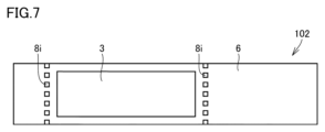
- FIG. 7 shows a plan view of the module according to the present embodiment.
- the module 102 has a groove 8i instead of the groove 8 described in the first embodiment.
- the groove 8i is in a dotted line shape.
- the groove may be in a dotted line shape like this.
- the shape of each element constituting the dotted line as the groove 8i is shown as a square, but this is merely an example.
- the shape of each element of the dotted line may be a rectangle, a polygon, a circle, an ellipse, or the like.
- the dotted lines as the groove 8i do not need to be unified into a repetition of the same shape, and different shapes may be arranged in combination.
- the groove when viewed in a plan view, the groove is a dotted line, meaning that there are places where the groove is interrupted.
- the sealing resin layer 6 is connected at the places where the groove is interrupted.
- the sealing resin layer 6 on both sides of the groove 8 is connected at some places, which increases the strength of the entire module.
- the grooves are dotted lines when viewed in a plan view, but the grooves may be dashed lines.
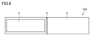
- FIG. 8 shows a plan view of the module according to the third embodiment.
- the module 103 is rectangular, and the semiconductor component 3 is disposed in the module 103 at a position close to one end.
- the groove 8 is provided along the short side of the semiconductor component 3.
- the groove 8 is provided so as to divide the sealing resin layer 6.
- the groove 8 is provided so as to extend from a point midway along one long side of the module 103 to a point midway along the other long side.
- the effects described in the first embodiment can be obtained.
- a configuration like a module 104 shown in Fig. 9 may be used.
- the module 104 has a rectangular shape when viewed in a plan view, and the semiconductor component 3 is arranged so as to occupy a substantially fixed section in the middle of the module 104.
- the grooves 8 are arranged so as to extend along each of the two short sides of the semiconductor component 3.
- the two grooves 8 are each provided so as to extend from one long side of the module 104 to the other long side.
- Module 105 is rectangular when viewed in a plan view, and semiconductor component 3 is disposed near one corner of module 105.
- Groove 8 is provided in an L-shape so as to surround semiconductor component 3 near one corner of module 105.
- Module 106 is rectangular when viewed in a plan view, and semiconductor component 3 is arranged midway along one of the sides of the outline of module 106. Groove 8 is provided so as to surround semiconductor component 3 of module 106 from three sides.
- module 107 a configuration like module 107 shown in FIG. 12 may be used.
- semiconductor component 3 is disposed in the middle, away from any side.
- Groove 8 is provided so as to completely surround semiconductor component 3.
- Groove 8 is provided in an annular shape. As exemplified here, it is preferable that groove 8 is disposed so as to surround semiconductor component 3 when viewed from a direction perpendicular to main surface 1a.
- the semiconductor component 3 When viewed from a direction perpendicular to the main surface 1a, the semiconductor component 3 is preferably arranged so that at least one side of the semiconductor component 3 follows the outline of the substrate 1, and the groove 8 is preferably provided so as to be spaced apart from the semiconductor component 3 and follow one of the sides of the semiconductor component 3 that does not follow the outline of the substrate 1.
- the outline of the substrate 1 can be used to effectively position the semiconductor component 3 while keeping the required length of the groove 8 short.
- the groove can be omitted, thereby keeping the amount of work required to form the groove to a minimum.
- one module may include two or more semiconductor components 3. In the case where one module includes two or more semiconductor components 3, two or more of the above-mentioned embodiments may be selected for each semiconductor component 3 and used in appropriate combination.
- Appendix 5 3. The module described in appendix 1 or 2, wherein, when viewed from a direction perpendicular to the main surface, the semiconductor component is arranged such that at least one edge of the semiconductor component follows an outline of the substrate, and the groove is spaced apart from the semiconductor component and follows one of the edges of the semiconductor component that does not follow the outline of the substrate.
Landscapes
- Engineering & Computer Science (AREA)
- Microelectronics & Electronic Packaging (AREA)
- Structures Or Materials For Encapsulating Or Coating Semiconductor Devices Or Solid State Devices (AREA)
Abstract
モジュールは、主面(1a)を有する基板(1)と、主面(1a)に実装された半導体部品(3)と、主面(1a)および半導体部品(3)の側面を封止するように封止樹脂で形成された封止樹脂層(6)とを備え、半導体部品(3)は、部品本体(31)と、部品本体(31)の基板(1)側の面に接続されたバンプ(32)とを備える。半導体部品(3)の主面(1a)に対する実装は、部品本体(31)を主面(1a)から離隔させた状態でバンプ(32)を主面(1a)に接続することによって行なわれており、部品本体(31)と主面(1a)との間の隙間には、アンダーフィル樹脂が充填されることによってアンダーフィル層(7)が形成されており、アンダーフィル樹脂の弾性係数は、前記封止樹脂の弾性係数よりも低く、アンダーフィル層(7)は、部品本体(31)を主面(1a)に投影した領域の外へはみ出して存在するはみ出し部分(7e)を含む。はみ出し部分(7e)は、封止樹脂層(6)によって覆われている。はみ出し部分(7e)を封止樹脂層(6)の基板(1)から遠い側の面に投影した領域内において、封止樹脂層(6)に溝(8)が形成されている。
Description
本発明は、モジュールに関するものである。
高周波モジュールにおいて、温度サイクル条件のもとでの部品内蔵基板とマザー基板との接合部の破損の問題に対処するために、半導体部品と外部接続端子との間に溝を形成した構成が、特開2021-197568号公報(特許文献1)に記載されている。
パッケージ部品を基板に実装して樹脂で封止した構造のモールドパッケージにおいて、熱膨張および熱収縮に起因する応力がパッケージ部品に加わることを抑制するために樹脂の上面から下面に向けて溝部が形成された構成が、特開2015-2245号公報(特許文献2)に記載されている。
基板の主面に複数の部品が実装され、封止樹脂層で封止された構造のモジュールにおいて、封止樹脂層の上面から基板の主面に向かって凹みが形成された構成が、国際公開WO2018/194012A1(特許文献3)に記載されている。封止樹脂層の凹み内部以外の表面はシールド層によって覆われている。この文献では、部品が発した不要な電磁波は封止樹脂層に形成された凹みから効果的にモジュール外へ出て行くので、他の部品に到達しにくくなるとされている。
特許文献1~3に示された構成では、実装された部品の側面に近い位置で封止樹脂部に溝が形成されている。この溝は、応力緩和または電磁波干渉防止を目的としたものである。
ところで、曲げによる応力の作用には、実装された部品の下側における封止樹脂と基板との間の線膨張係数の差による影響が大きい。実装される部品のサイズが大きい場合には、部品の側面の近傍に溝を設けるだけでは応力対策が不十分であった。
そこで、本発明は、基板に実装される半導体部品のサイズが大きい場合であっても、曲げによる応力を緩和することができるモジュールを提供することを目的とする。
上記目的を達成するため、本発明に基づくモジュールは、主面を有する基板と、上記主面に実装された半導体部品と、上記主面および上記半導体部品の側面を封止するように封止樹脂で形成された封止樹脂層とを備え、上記半導体部品は、部品本体と、上記部品本体の上記基板側の面に接続されたバンプとを備える。上記半導体部品の上記主面に対する実装は、上記部品本体を上記主面から離隔させた状態で上記バンプを上記主面に接続することによって行なわれている。上記部品本体と上記主面との間の隙間には、アンダーフィル樹脂が充填されることによってアンダーフィル層が形成されている。上記アンダーフィル樹脂の弾性係数は、上記封止樹脂の弾性係数よりも低い。上記アンダーフィル層は、上記部品本体を上記主面に投影した領域の外へはみ出して存在するはみ出し部分を含む。上記はみ出し部分は、上記封止樹脂層によって覆われている。上記はみ出し部分を上記封止樹脂層の上記基板から遠い側の面に投影した領域内において、上記封止樹脂層に溝が形成されている。
本発明によれば、半導体部品と基板との間の線膨張係数の差によって生じる応力は、アンダーフィル層によって緩和され、さらに、封止樹脂層と半導体部品との間の線膨張係数の差によって生じる応力は、溝によって緩和されるので、基板に実装される半導体部品のサイズが大きい場合であっても、曲げによる応力を緩和することができる。
図面において示す寸法比は、必ずしも忠実に現実のとおりを表しているとは限らず、説明の便宜のために寸法比を誇張して示している場合がある。以下の説明において、上または下の概念に言及する際には、絶対的な上または下を意味するとは限らず、図示された姿勢の中での相対的な上または下を意味する場合がある。
(実施の形態1)
図1~図3を参照して、本発明に基づく実施の形態1におけるモジュールについて説明する。本実施の形態におけるモジュールの断面図を図1に示す。図1におけるZ1部の拡大図を図2に示す。
図1~図3を参照して、本発明に基づく実施の形態1におけるモジュールについて説明する。本実施の形態におけるモジュールの断面図を図1に示す。図1におけるZ1部の拡大図を図2に示す。
本実施の形態におけるモジュール101は、主面1aを有する基板1と、主面1aに実装された半導体部品3と、主面1aおよび半導体部品3の側面を封止するように封止樹脂で形成された封止樹脂層6とを備える。半導体部品3は、たとえばIC(Integrated Circuit)であってよい。半導体部品3の上面は封止樹脂層6から露出していてよい。封止樹脂層6の上面および側面を覆うようにシールド膜が設けられていてもよい。シールド膜は金属膜である。半導体部品3の上面もシールド膜で覆われていてもよい。なお、本実施の形態では、シールド膜がない例を示している。
基板1の主面1aには、半導体部品3の他に、部品41,42,43,44が実装されている。
半導体部品3は、部品本体31と、部品本体31の基板1側の面に接続されたバンプ32とを備える。半導体部品3の主面1aに対する実装は、部品本体31を主面1aから離隔させた状態でバンプ32を主面1aに接続することによって行なわれている。部品本体31と主面1aとの間の隙間には、アンダーフィル樹脂が充填されることによってアンダーフィル層7が形成されている。アンダーフィル樹脂の弾性係数は、封止樹脂の弾性係数よりも低い。アンダーフィル層7は、部品本体31を主面1aに投影した領域の外へはみ出して存在するはみ出し部分7eを含む。はみ出し部分7eは、封止樹脂層6によって覆われている。はみ出し部分7eを封止樹脂層6の基板1から遠い側の面に投影した領域内において、封止樹脂層6に溝8が形成されている。
図1における溝8の底近傍の拡大図を図2に示す。本実施の形態におけるモジュール101の平面図を図3に示す。図2に示したように溝8はアンダーフィル層7のはみ出し部分7eに入り込んでいるが、主面1aには到達していない。溝8の底は、断面図で見たときU字形状となっている。溝8の底は、アンダーフィル層7の中にある。ここで示す例では、アンダーフィル層7は、部分7cとはみ出し部分7eとを含む。部分7cは、アンダーフィル層7のうち、部品本体31を主面1aに投影した領域にある部分である。はみ出し部分7eは、アンダーフィル層7が、部分7cから連続してその外側へとはみ出した部分である。ここで示す例では、はみ出し部分7eは、部分7cから連続して延在しているが、断面図で見たとき、はみ出し部分7eは、部分7cから完全に連続しているとは限らない。アンダーフィル層7は、断面図で見たとき、部分7cからはみ出し部分7eの先端に至るまでの途中で途切れていてもよい。
図3に示したように、主面1aに垂直な方向から見たとき、溝8は、半導体部品3から離隔しつつ半導体部品3の辺に沿うように形成されている。ここで示す例では、モジュール101は短冊形状であり、その長手方向の中間部分において、モジュール101の幅のほとんどを占めるように半導体部品3が配置されている。
本実施の形態では、半導体部品3と基板1との間の線膨張係数の差によって生じる応力は、アンダーフィル層7によって緩和される。さらに、封止樹脂層6と半導体部品3との間の線膨張係数の差によって生じる応力は、溝8によって緩和される。さらに、溝8の底がアンダーフィル層7の中にあるような構成とすることによって、破壊耐性が向上する。したがって、本実施の形態では、基板に実装される半導体部品のサイズが大きい場合であっても、曲げによる応力を緩和することができるモジュールを実現することができる。
なお、断面図で見たときの溝8の底の形状は、図4に示すようにU字形状であってもよいが、他の形状であってもよい。たとえば図5に示すように矩形状であってもよい。たとえば図6に示すようにV字形状であってもよい。
なお、本実施の形態では、溝8の底は、はみ出し部分7eに入り込んでいるが主面1aには到達していないことが好ましい。溝8の底がはみ出し部分7eまで到達しない程度の深さであっても、一応の効果はある。しかし、本実施の形態で示したように、溝8の底がはみ出し部分7eに入り込んでいることにより、この位置における封止樹脂層6内での応力の伝達を遮断することができるので好ましい。
なお、本実施の形態で示したように、主面1aに垂直な方向から見たとき、溝8は、半導体部品3から離隔しつつ半導体部品3の辺に沿うように形成されていることが好ましい。この構成を採用することにより、封止樹脂層6と半導体部品3との間の線膨張係数の差によって生じる応力を、効率良く遮断することができる。
なお、封止樹脂とアンダーフィル樹脂とでは、フィラーの含有条件が異なることが好ましい。この構成を採用することにより、両者の間に容易に弾性係数の差を設けることができる。各樹脂が主材料とフィラーとの組合せであるとすると、封止樹脂の主材料とアンダーフィル樹脂の主材料とは、同じであってもよい。たとえば、アンダーフィル樹脂と封止樹脂との両方がエポキシ樹脂を主材料としていてもよい。フィラーの含有条件とは、フィラーの含有量、フィラーの平均径、フィラーの形状、フィラーの材質などを含む概念である。主材料の条件が同じであっても、フィラーの含有条件を変えることで、弾性係数を変化させることができる。フィラーの含有条件を変えることで、その樹脂を、所望の弾性係数となるように調整することも可能である。
(実施の形態2)
図7を参照して、本発明に基づく実施の形態2におけるモジュールについて説明する。本実施の形態におけるモジュールの平面図を図7に示す。モジュール102は、実施の形態1で説明した溝8の代わりに溝8iを有する。平面図で見たときに、溝8iは点線状となっている。溝は、このように点線状であってもよい。図7では、溝8iとしての点線を構成する各要素の形状が正方形であるように表示されているが、これはあくまで一例である。点線の各要素の形状は、矩形、多角形、円形、楕円形などであってもよい。また、溝8iとしての点線は、同じ形状の繰り返しに統一する必要はなく、異なる形状が組み合わせて配置されていてもよい。
図7を参照して、本発明に基づく実施の形態2におけるモジュールについて説明する。本実施の形態におけるモジュールの平面図を図7に示す。モジュール102は、実施の形態1で説明した溝8の代わりに溝8iを有する。平面図で見たときに、溝8iは点線状となっている。溝は、このように点線状であってもよい。図7では、溝8iとしての点線を構成する各要素の形状が正方形であるように表示されているが、これはあくまで一例である。点線の各要素の形状は、矩形、多角形、円形、楕円形などであってもよい。また、溝8iとしての点線は、同じ形状の繰り返しに統一する必要はなく、異なる形状が組み合わせて配置されていてもよい。
本実施の形態では、平面図で見たときに、溝が点線状であるので、溝の途中に途切れている箇所がある。このように溝が途切れた箇所では封止樹脂層6がつながっている。このように溝8の両側の封止樹脂層6が一部の箇所でつながっているので、モジュール全体での強度を上げることができる。
なお、本実施の形態では、平面図で見たときに溝が点線状である例を示したが、溝は破線状であってもよい。
(実施の形態3)
図8を参照して、本発明に基づく実施の形態3におけるモジュールについて説明する。本実施の形態におけるモジュールの平面図を図8に示す。
図8を参照して、本発明に基づく実施の形態3におけるモジュールについて説明する。本実施の形態におけるモジュールの平面図を図8に示す。
この例では、モジュール103は短冊形状であり、半導体部品3は、モジュール103の中で一方の端に近い位置に配置されている。溝8は、半導体部品3の短辺に沿って設けられている。溝8は、封止樹脂層6を分断するように設けられている。溝8は、モジュール103の一方の長辺の途中の点から他方の長辺の途中の点に至るように設けられている。
本実施の形態においても、実施の形態1で説明した効果を得ることができる。
なお、本実施の形態におけるモジュールの変形例として、図9に示すモジュール104のような構成であってもよい。モジュール104は平面図で見たときに短冊形状であり、半導体部品3は、モジュール104の途中の一定区間をほぼ占めるように配置されている。溝8は、半導体部品3の2本の短辺にそれぞれ沿うように配置されている。2本の溝8は、それぞれモジュール104の一方の長辺から他方の長辺に至るように設けられている。
なお、本実施の形態におけるモジュールの変形例として、図9に示すモジュール104のような構成であってもよい。モジュール104は平面図で見たときに短冊形状であり、半導体部品3は、モジュール104の途中の一定区間をほぼ占めるように配置されている。溝8は、半導体部品3の2本の短辺にそれぞれ沿うように配置されている。2本の溝8は、それぞれモジュール104の一方の長辺から他方の長辺に至るように設けられている。
本実施の形態におけるモジュールのさらなる変形例として、図10に示すモジュール105のような構成であってもよい。モジュール105は、平面図で見たときに矩形状であり、半導体部品3は、モジュール105の1つのコーナーの近傍に配置されている。溝8は、モジュール105の1つのコーナーの近傍において半導体部品3を囲むようにL字形状に設けられている。
本実施の形態におけるモジュールのさらなる変形例として、図11に示すモジュール106のような構成であってもよい。モジュール106は、平面図で見たときに矩形状であり、半導体部品3は、モジュール106の外形線のうち1本の辺の途中においてこの辺に沿うように配置されている。溝8は、モジュール106の半導体部品3を三方から囲むように設けられている。
本実施の形態におけるモジュールのさらなる変形例として、図12に示すモジュール107のような構成であってもよい。モジュール107においては、半導体部品3は、いずれの辺からも離れた中ほどに配置されている。溝8は、半導体部品3を完全に取り囲むように設けられている。溝8は、環状に設けられている。ここで例示したように、主面1aに垂直な方向から見たとき、溝8は、半導体部品3を取り囲むように配置されていることが好ましい。
主面1aに垂直な方向から見たとき、半導体部品3は半導体部品3の少なくとも1本の辺が基板1の外形線に沿うように配置されており、溝8は、半導体部品3から離隔しつつ半導体部品3の辺のうち基板1の外形線に沿っていない辺に沿うように設けられていることが好ましい。この構成を採用することにより、基板1の外形線を利用して半導体部品3をうまく配置しつつ、溝8の必要な長さを少なく抑えることができる。また、半導体部品3の辺が基板の外形線に沿っている部分では、溝を省略することができるので、溝を形成するための作業量を少なく抑えることができる。
なお、上記実施の形態のうち複数を適宜組み合わせて採用してもよい。また、1つのモジュールの中に備わる半導体部品3の個数は1個とは限らない。1つのモジュールが複数の半導体部品3を備えていてもよい。1つのモジュールが複数の半導体部品3を備える場合は、個々の半導体部品3に対して、上記実施の形態のうち複数を選択して適宜組み合わせて採用してもよい。
なお、今回開示した上記実施の形態はすべての点で例示であって制限的なものではない。本発明の範囲は請求の範囲によって示され、請求の範囲と均等の意味および範囲内でのすべての変更を含むものである。
(付記)
(付記1)
主面を有する基板と、
前記主面に実装された半導体部品と、
前記主面および前記半導体部品の側面を封止するように封止樹脂で形成された封止樹脂層とを備え、
前記半導体部品は、部品本体と、前記部品本体の前記基板側の面に接続されたバンプとを備え、
前記半導体部品の前記主面に対する実装は、前記部品本体を前記主面から離隔させた状態で前記バンプを前記主面に接続することによって行なわれており、
前記部品本体と前記主面との間の隙間には、アンダーフィル樹脂が充填されることによってアンダーフィル層が形成されており、
前記アンダーフィル樹脂の弾性係数は、前記封止樹脂の弾性係数よりも低く、
前記アンダーフィル層は、前記部品本体を前記主面に投影した領域の外へはみ出して存在するはみ出し部分を含み、
前記はみ出し部分は、前記封止樹脂層によって覆われており、
前記はみ出し部分を前記封止樹脂層の前記基板から遠い側の面に投影した領域内において、前記封止樹脂層に溝が形成されている、モジュール。
(付記1)
主面を有する基板と、
前記主面に実装された半導体部品と、
前記主面および前記半導体部品の側面を封止するように封止樹脂で形成された封止樹脂層とを備え、
前記半導体部品は、部品本体と、前記部品本体の前記基板側の面に接続されたバンプとを備え、
前記半導体部品の前記主面に対する実装は、前記部品本体を前記主面から離隔させた状態で前記バンプを前記主面に接続することによって行なわれており、
前記部品本体と前記主面との間の隙間には、アンダーフィル樹脂が充填されることによってアンダーフィル層が形成されており、
前記アンダーフィル樹脂の弾性係数は、前記封止樹脂の弾性係数よりも低く、
前記アンダーフィル層は、前記部品本体を前記主面に投影した領域の外へはみ出して存在するはみ出し部分を含み、
前記はみ出し部分は、前記封止樹脂層によって覆われており、
前記はみ出し部分を前記封止樹脂層の前記基板から遠い側の面に投影した領域内において、前記封止樹脂層に溝が形成されている、モジュール。
(付記2)
前記溝の底は、前記はみ出し部分に入り込んでいるが前記主面には到達していない、付記1に記載のモジュール。
前記溝の底は、前記はみ出し部分に入り込んでいるが前記主面には到達していない、付記1に記載のモジュール。
(付記3)
前記主面に垂直な方向から見たとき、前記溝は、前記半導体部品から離隔しつつ前記半導体部品の辺に沿うように形成されている、付記1または2に記載のモジュール。
前記主面に垂直な方向から見たとき、前記溝は、前記半導体部品から離隔しつつ前記半導体部品の辺に沿うように形成されている、付記1または2に記載のモジュール。
(付記4)
前記主面に垂直な方向から見たとき、前記溝は、前記半導体部品を取り囲むように配置されている、付記3に記載のモジュール。
前記主面に垂直な方向から見たとき、前記溝は、前記半導体部品を取り囲むように配置されている、付記3に記載のモジュール。
(付記5)
前記主面に垂直な方向から見たとき、前記半導体部品は前記半導体部品の少なくとも1本の辺が前記基板の外形線に沿うように配置されており、前記溝は、前記半導体部品から離隔しつつ前記半導体部品の辺のうち前記基板の外形線に沿っていない辺に沿うように設けられている、付記1または2に記載のモジュール。
前記主面に垂直な方向から見たとき、前記半導体部品は前記半導体部品の少なくとも1本の辺が前記基板の外形線に沿うように配置されており、前記溝は、前記半導体部品から離隔しつつ前記半導体部品の辺のうち前記基板の外形線に沿っていない辺に沿うように設けられている、付記1または2に記載のモジュール。
(付記6)
前記封止樹脂と前記アンダーフィル樹脂とでは、フィラーの含有条件が異なる、付記1から5のいずれか1項に記載のモジュール。
前記封止樹脂と前記アンダーフィル樹脂とでは、フィラーの含有条件が異なる、付記1から5のいずれか1項に記載のモジュール。
1 基板、1a 主面、3 半導体部品、6 封止樹脂層、7 アンダーフィル層、7c 部分、7e はみ出し部分、8,8i 溝、31 部品本体、32 バンプ、41,42,43,44 部品、101,102,103,104,105,106,107 モジュール。
Claims (6)
- 主面を有する基板と、
前記主面に実装された半導体部品と、
前記主面および前記半導体部品の側面を封止するように封止樹脂で形成された封止樹脂層とを備え、
前記半導体部品は、部品本体と、前記部品本体の前記基板側の面に接続されたバンプとを備え、
前記半導体部品の前記主面に対する実装は、前記部品本体を前記主面から離隔させた状態で前記バンプを前記主面に接続することによって行なわれており、
前記部品本体と前記主面との間の隙間には、アンダーフィル樹脂が充填されることによってアンダーフィル層が形成されており、
前記アンダーフィル樹脂の弾性係数は、前記封止樹脂の弾性係数よりも低く、
前記アンダーフィル層は、前記部品本体を前記主面に投影した領域の外へはみ出して存在するはみ出し部分を含み、
前記はみ出し部分は、前記封止樹脂層によって覆われており、
前記はみ出し部分を前記封止樹脂層の前記基板から遠い側の面に投影した領域内において、前記封止樹脂層に溝が形成されている、モジュール。 - 前記溝の底は、前記はみ出し部分に入り込んでいるが前記主面には到達していない、請求項1に記載のモジュール。
- 前記主面に垂直な方向から見たとき、前記溝は、前記半導体部品から離隔しつつ前記半導体部品の辺に沿うように形成されている、請求項1または2に記載のモジュール。
- 前記主面に垂直な方向から見たとき、前記溝は、前記半導体部品を取り囲むように配置されている、請求項3に記載のモジュール。
- 前記主面に垂直な方向から見たとき、前記半導体部品は前記半導体部品の少なくとも1本の辺が前記基板の外形線に沿うように配置されており、前記溝は、前記半導体部品から離隔しつつ前記半導体部品の辺のうち前記基板の外形線に沿っていない辺に沿うように設けられている、請求項1または2に記載のモジュール。
- 前記封止樹脂と前記アンダーフィル樹脂とでは、フィラーの含有条件が異なる、請求項1から5のいずれか1項に記載のモジュール。
Applications Claiming Priority (2)
| Application Number | Priority Date | Filing Date | Title |
|---|---|---|---|
| JP2023-107101 | 2023-06-29 | ||
| JP2023107101 | 2023-06-29 |
Publications (1)
| Publication Number | Publication Date |
|---|---|
| WO2025004473A1 true WO2025004473A1 (ja) | 2025-01-02 |
Family
ID=93938598
Family Applications (1)
| Application Number | Title | Priority Date | Filing Date |
|---|---|---|---|
| PCT/JP2024/011375 Ceased WO2025004473A1 (ja) | 2023-06-29 | 2024-03-22 | モジュール |
Country Status (1)
| Country | Link |
|---|---|
| WO (1) | WO2025004473A1 (ja) |
Citations (4)
| Publication number | Priority date | Publication date | Assignee | Title |
|---|---|---|---|---|
| JPH11220077A (ja) * | 1997-10-15 | 1999-08-10 | Toshiba Corp | 半導体装置および半導体装置の製造方法 |
| JP2001308230A (ja) * | 2000-04-25 | 2001-11-02 | Matsushita Electric Ind Co Ltd | 半導体装置 |
| JP2009071251A (ja) * | 2007-09-18 | 2009-04-02 | Yokogawa Electric Corp | フリップチップbga基板 |
| US8378476B2 (en) * | 2010-03-25 | 2013-02-19 | Stats Chippac Ltd. | Integrated circuit packaging system with stacking option and method of manufacture thereof |
-
2024
- 2024-03-22 WO PCT/JP2024/011375 patent/WO2025004473A1/ja not_active Ceased
Patent Citations (4)
| Publication number | Priority date | Publication date | Assignee | Title |
|---|---|---|---|---|
| JPH11220077A (ja) * | 1997-10-15 | 1999-08-10 | Toshiba Corp | 半導体装置および半導体装置の製造方法 |
| JP2001308230A (ja) * | 2000-04-25 | 2001-11-02 | Matsushita Electric Ind Co Ltd | 半導体装置 |
| JP2009071251A (ja) * | 2007-09-18 | 2009-04-02 | Yokogawa Electric Corp | フリップチップbga基板 |
| US8378476B2 (en) * | 2010-03-25 | 2013-02-19 | Stats Chippac Ltd. | Integrated circuit packaging system with stacking option and method of manufacture thereof |
Similar Documents
| Publication | Publication Date | Title |
|---|---|---|
| JP5039058B2 (ja) | 半導体素子の実装構造体 | |
| JP6293030B2 (ja) | 電力用半導体装置 | |
| KR101922783B1 (ko) | 베이스판, 및 베이스판을 구비한 반도체 장치 | |
| US20180092201A1 (en) | High-frequency module | |
| CN111446218B (zh) | 芯片封装体 | |
| CN101752327B (zh) | 具有散热结构的半导体封装件 | |
| JP2005235997A (ja) | プリント基板、電子回路基板及びその製造方法 | |
| JP6092645B2 (ja) | 半導体装置 | |
| JP2015056638A (ja) | 半導体装置およびその製造方法 | |
| JP2008251731A (ja) | 半導体装置 | |
| JP2008124176A (ja) | 電力用半導体装置 | |
| JPH0223640A (ja) | 樹脂封止型半導体装置 | |
| TWI546914B (zh) | 部分圓頂封裝技術 | |
| JP5273265B2 (ja) | 電力用半導体装置 | |
| US20080251283A1 (en) | Mounting substrate and electronic device | |
| US9870977B2 (en) | Semiconductor device with heat information mark | |
| JP2010141043A (ja) | 半導体装置 | |
| JP5308979B2 (ja) | 半導体パッケージ | |
| WO2014196172A1 (ja) | モールドパッケージおよびその製造方法 | |
| JP7019840B2 (ja) | 半導体装置および半導体装置の製造方法 | |
| CN114937645B (zh) | 芯片封装结构 | |
| JP4154464B2 (ja) | 電子部品アセンブリの製造方法 | |
| US20060202350A1 (en) | Semiconductor device | |
| JP6964437B2 (ja) | 電子モジュール | |
| JP2014143371A (ja) | 回路基板 |
Legal Events
| Date | Code | Title | Description |
|---|---|---|---|
| 121 | Ep: the epo has been informed by wipo that ep was designated in this application |
Ref document number: 24831350 Country of ref document: EP Kind code of ref document: A1 |
|
| NENP | Non-entry into the national phase |
Ref country code: DE |